EP3754540A1 - Optical fingerprint recognition apparatus, electronic device and fingerprint recognition method - Google Patents
Optical fingerprint recognition apparatus, electronic device and fingerprint recognition method Download PDFInfo
- Publication number
- EP3754540A1 EP3754540A1 EP19813221.9A EP19813221A EP3754540A1 EP 3754540 A1 EP3754540 A1 EP 3754540A1 EP 19813221 A EP19813221 A EP 19813221A EP 3754540 A1 EP3754540 A1 EP 3754540A1
- Authority
- EP
- European Patent Office
- Prior art keywords
- visible light
- light source
- fingerprint identification
- fingerprint
- light emitting
- Prior art date
- Legal status (The legal status is an assumption and is not a legal conclusion. Google has not performed a legal analysis and makes no representation as to the accuracy of the status listed.)
- Granted
Links
Images




Classifications
-
- G—PHYSICS
- G06—COMPUTING OR CALCULATING; COUNTING
- G06V—IMAGE OR VIDEO RECOGNITION OR UNDERSTANDING
- G06V40/00—Recognition of biometric, human-related or animal-related patterns in image or video data
- G06V40/10—Human or animal bodies, e.g. vehicle occupants or pedestrians; Body parts, e.g. hands
- G06V40/12—Fingerprints or palmprints
- G06V40/13—Sensors therefor
- G06V40/1324—Sensors therefor by using geometrical optics, e.g. using prisms
-
- G—PHYSICS
- G06—COMPUTING OR CALCULATING; COUNTING
- G06V—IMAGE OR VIDEO RECOGNITION OR UNDERSTANDING
- G06V40/00—Recognition of biometric, human-related or animal-related patterns in image or video data
- G06V40/10—Human or animal bodies, e.g. vehicle occupants or pedestrians; Body parts, e.g. hands
- G06V40/12—Fingerprints or palmprints
- G06V40/1382—Detecting the live character of the finger, i.e. distinguishing from a fake or cadaver finger
-
- G—PHYSICS
- G06—COMPUTING OR CALCULATING; COUNTING
- G06V—IMAGE OR VIDEO RECOGNITION OR UNDERSTANDING
- G06V10/00—Arrangements for image or video recognition or understanding
- G06V10/10—Image acquisition
- G06V10/12—Details of acquisition arrangements; Constructional details thereof
- G06V10/14—Optical characteristics of the device performing the acquisition or on the illumination arrangements
- G06V10/141—Control of illumination
-
- G—PHYSICS
- G06—COMPUTING OR CALCULATING; COUNTING
- G06V—IMAGE OR VIDEO RECOGNITION OR UNDERSTANDING
- G06V40/00—Recognition of biometric, human-related or animal-related patterns in image or video data
- G06V40/10—Human or animal bodies, e.g. vehicle occupants or pedestrians; Body parts, e.g. hands
- G06V40/12—Fingerprints or palmprints
- G06V40/13—Sensors therefor
- G06V40/1318—Sensors therefor using electro-optical elements or layers, e.g. electroluminescent sensing
-
- H—ELECTRICITY
- H04—ELECTRIC COMMUNICATION TECHNIQUE
- H04N—PICTORIAL COMMUNICATION, e.g. TELEVISION
- H04N23/00—Cameras or camera modules comprising electronic image sensors; Control thereof
- H04N23/56—Cameras or camera modules comprising electronic image sensors; Control thereof provided with illuminating means
-
- G—PHYSICS
- G06—COMPUTING OR CALCULATING; COUNTING
- G06V—IMAGE OR VIDEO RECOGNITION OR UNDERSTANDING
- G06V40/00—Recognition of biometric, human-related or animal-related patterns in image or video data
- G06V40/10—Human or animal bodies, e.g. vehicle occupants or pedestrians; Body parts, e.g. hands
- G06V40/12—Fingerprints or palmprints
- G06V40/1341—Sensing with light passing through the finger
-
- G—PHYSICS
- G06—COMPUTING OR CALCULATING; COUNTING
- G06V—IMAGE OR VIDEO RECOGNITION OR UNDERSTANDING
- G06V40/00—Recognition of biometric, human-related or animal-related patterns in image or video data
- G06V40/10—Human or animal bodies, e.g. vehicle occupants or pedestrians; Body parts, e.g. hands
- G06V40/12—Fingerprints or palmprints
- G06V40/1382—Detecting the live character of the finger, i.e. distinguishing from a fake or cadaver finger
- G06V40/1394—Detecting the live character of the finger, i.e. distinguishing from a fake or cadaver finger using acquisition arrangements
Definitions
- the present application relates to the field of information technologies, and in particular, to an optical fingerprint identification apparatus, an electronic device and a fingerprint identification method.
- a fingerprint identification technology has been widely applied to various fields such as a mobile terminal, a smart home.
- visible light with a certain wavelength is adopted to illuminate a biological feature, and a reflected light signal carrying biological feature information is transmitted to a sensor for capturing by utilizing a reflection imaging principle of visible light, and legitimacy of a user identity is confirmed by comparing the captured information with a biological feature registered and stored in advance.
- a fingerprint sensor can only passively receive a reflected visible light signal for fingerprint identification, thereby limiting flexible selection of a wavelength of excitation light used for imaging.
- Embodiments of the present application provides an optical fingerprint identification apparatus, an electronic device and a fingerprint identification method, which could flexibly select a wavelength of excitation light used for fingerprint identification, improve an ability to distinguish between real and fake fingers, and further improve safety of fingerprint identification.
- an optical fingerprint identification apparatus applied to an electronic device having a display screen, including: at least one non-visible light source, configured to emit non-visible light to a human finger to provide excitation light for fingerprint identification, where a number of light emitting wave bands of the non-visible light source is at least 1; an optical component, disposed under a fingerprint detecting area of the display screen, and configured to receive signal light scattered and reflected by the human finger and collimate and/or converge the signal light; and a fingerprint sensor, disposed under the optical component, and configured to perform imaging based on the signal light passing through the optical component, where a working wave band of the fingerprint sensor is the same as a light emitting wave band of the non-visible light source, a number of the working wave bands is the same as the number of the light emitting wave bands, and the fingerprint sensor is directly or indirectly electrically connected to the non-visible light source, and is configured to control the non-visible light source to actively emit light.
- the optical fingerprint identification apparatus further includes a filter disposed between the optical component and the fingerprint sensor, and a light passing wave band of the filter is the same as the light emitting wave band of the non-visible light source.
- a number of the non-visible light sources is greater than 1, the number of the light emitting wave bands of the non-visible light source is greater than or equal to 1, a number of light passing wave bands of the filter is equal to the number of light emitting wave bands of the non-visible light source, and the light emitting wave bands are in one-to-one correspondence with the light passing wave bands.
- the electronic device includes a cover glass, and the display screen and the non-visible light source are disposed side by side under the cover glass.
- the non-visible light source is disposed on at least one side of a universal serial bus USB interface of the electronic device.
- the display screen is an organic light-emitting diode OLED display screen.
- the display screen includes a display module and a backlight module, and the backlight module is capable of transmitting the non-visible light emitted by the non-visible light source.
- the optical component includes a collimator array
- the collimator array includes a plurality of collimating holes configured to collimate the signal light and direct the signal light to the fingerprint sensor.
- the optical component includes: at least one lens and a support; the lens is configured to converge the signal light and direct the signal light to the fingerprint sensor; and the support is configured to accommodate and fix the lens.
- the optical component includes at least one camera lens, a lens barrel and a lens holder; the camera lens is configured to converge the signal light and direct the signal light to the fingerprint sensor; the lens barrel is configured to accommodate the camera lens; and the lens holder is configured to fix the lens barrel.
- the lens barrel and the lens holder are of an integrated structure.
- the lens barrel and the lens holder are of a separate structure, and the lens barrel and the lens holder are fixed through threaded connection.
- the optical component includes a microlens array and a diaphragm array disposed under the microlens array;
- the microlens array includes a plurality of microlenses configured to converge the signal light;
- the diaphragm array includes a plurality of diaphragms, where the diaphragms are in one-to-one correspondence with the microlenses, and the diaphragms are configured to direct the signal light converged by the microlens to the fingerprint sensor.
- the fingerprint sensor includes a driving interface electrically connected to the non-visible light source, and is configured to directly control the non-visible light source to actively emit light.
- the optical fingerprint identification apparatus further includes a control module, and the fingerprint sensor is electrically connected to the non-visible light source through the control module; the fingerprint sensor is communicatively connected to the control module, and a driving interface of the control module is electrically connected to the non-visible light source; and the fingerprint sensor is configured to indirectly control the non-visible light source to actively emit light through the control module.
- the optical fingerprint identification apparatus includes two operating modes of a finger approaching detection mode and a fingerprint detection mode.
- the fingerprint sensor controls the non-visible light source to periodically and intermittently emit light, a light emitting period is a first period, a light emitting time of each period is a first light emitting time, a driving current output by the driving interface is a first driving current, and the first driving current is configured to drive the non-visible light source to actively emit light.
- the fingerprint sensor controls the non-visible light source to periodically and intermittently emit light
- a light emitting period of the non-visible light source is a second period
- a light emitting time of each period is a second light emitting time
- a driving current output by the driving interface is a second driving current
- the second driving current is configured to drive the non-visible light source to actively emit light
- the second period is greater than the first period
- the second light emitting time is greater than the first light emitting time
- the second driving current is greater than the first driving current.
- the fingerprint sensor includes a plurality of pixel units, and in the finger approaching detection mode, part of the pixel units perform imaging based on the signal light; and in the fingerprint detection mode, all of the pixel units perform imaging based on the signal light.
- an electronic device including a display screen configured to display a picture and detect presence of a contact input and the optical fingerprint identification apparatus in the first aspect or any possible implementation manner of the first aspect.
- a fingerprint identification method applied to the electronic device of the second aspect, and the fingerprint identification method includes: enabling a finger approaching detection mode, performing imaging based on signal light scattered and/or reflected from an object above a fingerprint capturing area when a non-visible light source illuminates the fingerprint capturing area, and determining whether an object is approaching; determining whether an object presses a display screen by pressing detection; if it is determined that an object is approaching, determining, according to a result of the pressing detection, whether pressing of the object is finger pressing or foreign body mistouching; if it is determined that the pressing of the object is the finger pressing, enabling a fingerprint detection mode, and performing imaging based on the signal light to obtain a fingerprint image.
- the enabling the finger approaching detection mode includes: controlling, by a fingerprint sensor, the non-visible light source to actively emit light, where the fingerprint sensor drives the non-visible light source through a driving current, a light emitting period of the non-visible light source is a first period, a light emitting time of each period is a first light emitting time, and the driving current is a first driving current.
- the if it is determined that the pressing of the object is the finger pressing, enabling the fingerprint detection mode includes: controlling, by the fingerprint sensor, the non-visible light source to actively emit light, the fingerprint sensor drives the non-visible light source through a driving current, a light emitting period of the non-visible light source is a second period, a light emitting time of each period is a second light emitting time, and the driving current is a second driving current; and the second period is greater than the first period, the second light emitting time is greater than the first light emitting time, and the second driving current is greater than the first driving current.
- a wavelength of excitation light used for fingerprint identification could be flexibly selected, an ability to distinguish between real and fake fingers is improved, and safety of fingerprint identification is further improved.
- a portable or mobile computing device such as a smart phone, a notebook computer, a tablet computer and a game device
- other electronic devices such as an electronic database, an automobile and an automated teller machine (Automated Teller Machine, ATM), which is not limited in the embodiments of the present application.
- a portable or mobile computing device such as a smart phone, a notebook computer, a tablet computer and a game device
- other electronic devices such as an electronic database, an automobile and an automated teller machine (Automated Teller Machine, ATM), which is not limited in the embodiments of the present application.
- ATM Automated Teller Machine
- an optical fingerprint identification apparatus provided in an embodiment of the present application may be applied to a smart phone, a tablet computer, and other electronic devices with a display screen or other electronic devices; More specifically, in the foregoing electronic device, the optical fingerprint identification apparatus may be disposed in a partial area or an entire area under a display screen, thereby forming an under-display (Under-display or Under-screen) optical fingerprint system.
- under-display Under-display or Under-screen
- FIG. 1 is a schematic structural diagram of an under-screen fingerprint identification apparatus.
- a display screen 150 may be an organic light-emitting diode (Organic Light-Emitting Diode, OLED) display screen, visible light emitted by a light emitting unit of the OLED display screen is configured to provide excitation light for fingerprint identification; when a finger is pressed against a fingerprint detecting area (not shown in FIG. 1 ) of the display screen 150, the excitation light is reflected by the finger and reaches an area under the display screen 150; and at this time, the reflected excitation light carries fingerprint information of the finger and becomes signal light.
- OLED Organic Light-Emitting Diode
- the signal light continues to be transmitted downward to reach an optical component 120; optionally, the optical component 120 may include a lens 121 configured to converge the signal light reflected by the finger to a photosensitive area 131 of a fingerprint sensor 130 to capture a fingerprint image.
- the optical component 120 may include a lens 121 configured to converge the signal light reflected by the finger to a photosensitive area 131 of a fingerprint sensor 130 to capture a fingerprint image.
- a lower part of FIG. 1 is a top view of the fingerprint sensor 130.
- a filter 140 may also be disposed between the optical component 120 and the fingerprint sensor 130, and the filter 140 is configured to filter stray light to obtain a better imaging effect.
- the fingerprint sensor 140 may only passively receive visible light emitted by the OLED display screen, thus limiting flexible selection of a wavelength of excitation light used for imaging.
- the optical fingerprint identification apparatus provided in the embodiment of the present application may flexibly select the wavelength of the excitation light used for imaging, improve an ability to distinguish between real and fake fingers, and further improve safety of fingerprint identification.
- FIG. 2 is a schematic structural diagram of an optical fingerprint identification apparatus according to an embodiment of the present application.
- An optical fingerprint identification apparatus 200 may be applied to an electronic device having a display screen, and includes at least one non-visible light source 210, an optical component 220, and a fingerprint sensor 230.
- the non-visible light source 210 emits non-visible light to a human finger to provide excitation light for fingerprint identification, and the number of light emitting wave bands of the non-visible light source 210 is at least 1.
- the optical fingerprint identification apparatus 200 may include the at least one non-visible light source 210, and if the number of non-visible light sources 210 is greater than 1, the number of light emitting wave bands of the non-visible light sources 210 is greater than or equal to 1, for example, when the optical fingerprint identification apparatus 200 includes two non-visible light sources 210, wavelengths of the two non-visible light sources 210 may be 850 nm and 940 nm, respectively, or may be both 850 nm, or may be both 940 nm.
- the number of non-visible light sources 210 and the number of light emitting wave bands are not limited in the embodiment of the present application, and are set according to requirements of an actual product.
- a plurality of non-visible light sources 210 adopt a same light emitting wave band, it has advantages of having high illumination intensity, obtaining stronger signal light for fingerprint detection, and acquiring a better fingerprint imaging effect; also when the plurality of non-visible light sources 210 are located in different positions, the finger may be imaged at different angles, and the fingerprint imaging effect may also be improved; and when the plurality of non-visible light sources 210 adopt different light emitting wave bands, in addition to increasing the illumination intensity, the finger may be imaged in different wave bands to obtain different imaging features.
- different objects have different transmittance for light with different wavelengths; for example, a finger has lower transmittance for light with a wavelength of 850 nm than that of light with a wavelength of 940 nm, and a fake finger and other foreign objects have relatively close transmittance for the foregoing light with the two wavelengths; therefore, when fingerprint imaging is performed, data of the real finger and data of the fake finger or other foreign objects will differ significantly; and this feature may be used to distinguish between the real finger and the fake finger and foreign object, improve an interception rate of fake finger attacks, that is, to improve the ability to distinguish between the real finger and the fake finger, and further improve security of fingerprint identification.
- the optical component 220 is disposed under a fingerprint detecting area of the display screen, is configured to receive signal light scattered and reflected by the human finger, and collimate or converge the signal light.
- the optical component 220 has higher transmittance for the non-visible light emitted by the non-visible light source 210.
- the optical component 220 may include a collimator array, and the collimator array includes a plurality of collimating holes configured to collimate the signal light and direct the signal light to the fingerprint sensor 230.
- the optical component 220 may include at least one lens and a holder.
- the lens is configured to converge the signal light and direct the signal light to the fingerprint sensor 230; the lens may increase an incident angle of a central field of view, increase convergence of the signal light and obtain a better imaging effect. It should be understood that the number of lenses may be multiple, so that a better convergence effect may be obtained, and at the same time, the lens may be a spherical lens or an aspheric lens, or a combination of a spherical lens and an aspheric lens, which is not limited in this embodiment.
- the support is configured to accommodate and fix the lens.
- the optical component 220 may include at least one camera lens, a lens barrel and a lens holder; the camera lens is configured to converge the signal light and direct the signal light to the fingerprint sensor 230; the lens barrel is configured to accommodate the camera lens; and the lens holder is configured to fix the lens barrel.
- the lens barrel and the lens holder may be of an integrated structure, or the lens barrel and the lens holder may be of a separate structure, and the lens barrel and the lens holder are fixed through threaded connection.
- the optical component 220 may include a microlens array and a diaphragm array disposed under the microlens array;
- the microlens array includes a plurality of microlenses configured to converge the signal light;
- the diaphragm array includes a plurality of diaphragms, where the diaphragms are in one-to-one correspondence with the microlenses, and the diaphragms are configured to direct the signal light converged by the microlens to the fingerprint sensor 230.
- the fingerprint sensor 230 is disposed under the optical component 220, and is configured to perform imaging based on the signal light passing through the optical component 220, where a working wave band of the fingerprint sensor 230 is the same as the light emitting wave band of the non-visible light source 210, the number of working wave bands is the same as the number of light emitting wave bands, and the fingerprint sensor 230 is directly or indirectly electrically connected to the non-visible light source 210, and is configured to control the non-visible light source 210 to actively emit light.
- the optical fingerprint identification apparatus 200 includes more than one non-visible light source 210 and the number of light emitting wave bands of the non-visible light source 210 is greater than 1, the number of working wave bands of the fingerprint sensor 230 is the same as the number of light emitting wave bands, and is also greater than 1, that is, there may be multiple working wave bands of the fingerprint sensor 230.
- wavelengths of the two non-visible light sources 210 may be 850 nm and 940 nm, respectively
- the number of working wave bands of the fingerprint sensor 230 is the same as the number of light emitting wave bands of the non-visible light sources 210, and there are also two wave bands, which are 850 nm and 940 nm, respectively, the fingerprint sensor 230 is not sensitive to light of other wave bands except 850 nm and 940 nm, and thus an influence of light of other wave bands on a fingerprint imaging effect may be reduced.
- the fingerprint sensor 230 is directly or indirectly electrically connected to the non-visible light source 210 (not shown in FIG. 2 ), and is configured to control the non-visible light source 210 to actively emit light, which may be referred to FIGS. 5 and 6 , and this embodiment will not be described in detail.
- FIG. 3 is a schematic diagram of an optical fingerprint identification apparatus performing fingerprint identification according to an embodiment of the present application, that is, it is a schematic diagram of the optical fingerprint identification apparatus 200 shown in FIG. 2 applied to an electronic device performing fingerprint identification.
- a fingerprint identification apparatus includes a non-visible light source 310, an optical component 320, and a fingerprint sensor 330, which have been described in detail in FIG. 2 and will not be repeatedly described herein.
- An electronic device may include a cover glass 360 for protecting a display screen 350, and the display screen 350 and the non-visible light source 310 may be disposed side by side under the cover glass 360. It should be understood that in order to prevent a user from seeing the non-visible light source 310 disposed under the cover glass through the cover glass 360, a layer of an isolation film (not shown in FIG. 3 ) may be disposed between the cover glass 360 and the non-visible light source 310, the isolation film may block visible light and has higher transmittance for the non-visible light emitted by the non-visible light source 310.
- the optical component 320 may be disposed under the display screen 350, specifically, may be located under a fingerprint detecting area (not shown in FIG. 3 ) of the display screen 350, and the fingerprint detecting area is located in part or all of a display area of the display screen.
- the fingerprint sensor 330 may be disposed under the optical component 320.
- the optical component 320 shown in this embodiment includes a lens 321 and a support 322.
- the lens 321 is configured to converge the signal light and direct the signal light to the fingerprint sensor 330; and the lens 321 may increase an incident angle of a central field of view, increase convergence of the signal light, and obtain a better imaging effect.
- the number of lenses 321 may be multiple, so that a better convergence effect may be obtained, and at the same time, the lens 321 may be a spherical lens or an aspheric lens, or a combination of a spherical lens and an aspheric lens, which is not limited in this embodiment.
- the support 322 is configured to accommodate and fix the lens 321.
- the optical component 320 in the optical fingerprint identification apparatus shown in FIG. 3 is merely illustrative, and the optical component 320 may also be an optical component including a collimator array, or an optical component including at least one camera lens, a lens barrel and a lens holder. Reference is made to the contents described in FIG. 2 , which will not be repeatedly described herein.
- a basic process of performing fingerprint identification by the optical fingerprint identification apparatus in this embodiment is as follows: the non-visible light emitted by the non-visible light source 310 is incident on the interior of a human finger pressed on the cover glass 360 through the cover glass 360, is scattered by tissues in the finger or is reflected by a finger surface, and then sequentially passes through the cover glass 360, the display screen 350 and the optical component 320, to reach the fingerprint sensor 330; and the scattered and/or reflected non-visible light carries fingerprint information of the finger to become the signal light, and the fingerprint sensor 330 is configured to perform imaging based on the signal light.
- the fingerprint sensor 330 may include a photosensitive area 331 which may include a plurality of pixel units. Therefore, the fingerprint sensor 330 is configured to perform imaging based on the signal light, which actually refers that the photosensitive area 331 of the fingerprint sensor 330 is configured to perform imaging based on the signal light.
- the optical fingerprint identification apparatus may also include a filter 340 which may be disposed in a light path between the display screen 350 and the fingerprint sensor 330.
- the filter 340 is disposed between the optical component 320 and the fingerprint sensor 330, and a light passing wave band of the filter 340 is the same as a light emitting wave band of the non-visible light source 310, and therefore the filter 340 can filter stray light and reduce interference of stray light in fingerprint identification.
- a film may be coated on a surface of the fingerprint sensor 330 by a vapor deposition process to form the filter 340, and other components may be used to fix the filter 340 between the optical component 320 and the fingerprint sensor 330, which is not limited in this embodiment and may be set according to an actual product requirement.
- the number of non-visible light sources 310 is greater than 1, the number of light emitting wave bands of the non-visible light sources 310 is greater than or equal to 1, the number of light passing wave bands of the filter 340 is equal to the number of light emitting wave bands of the non-visible light source 310, and the light emitting wave bands is in one-to-one correspondence with the light passing wave band. It should be understood that when the fingerprint identification apparatus includes more than one non-visible light source 310 and the number of light emitting wave bands of the non-visible light source 310 is greater than 1, the number of light passing wave bands of the filter 340 is the same as the number of light emitting wave bands, and is also greater than 1, that is, there may be multiple light passing wave bands of the filter 340.
- wavelengths of the two non-visible light sources 310 may be 850 nm and 940 nm, respectively
- the number of light passing wave bands of the filter 340 is the same as the number of light emitting wave bands of the non-visible light sources 310, and there are two wave bands, which are 850 nm and 940 nm, respectively.
- the display screen 350 may be an OLED display screen.
- the non-visible light source 310 in the optical fingerprint identification apparatus rather than visible light emitted by the OLED display screen is used as excitation light for fingerprint identification, which has advantages of flexibly selecting a wavelength of the excitation light for fingerprint identification, improving the ability to distinguish between real and fake fingers, and further improving safety of fingerprint identification.
- the optical fingerprint identification apparatus may also be applied to an electronic device having other types of display screen, for example, the display screen may include a display module and a backlight module, the backlight module is configured to provide a visible light source to make a display module display a picture, as shown in FIG. 4 .
- a display screen 450 includes a display module 451 and a backlight module 452.
- the display module 451 may be a liquid crystal module and the display screen 450 may be a liquid crystal display screen.
- An existing backlight module generally includes a point light source and a plurality of layers of laminated materials with different functions, and the laminated material includes a reflective film (also referred to as a mirror film), a light directing plate, a light homogenizing film (also referred to as a diffusion film) and a prism film (also referred to as a brightness enhancement film), and there are at least one layer of the light homogenizing film and at least one layer of the prism film.
- a purpose of combining these laminated materials is to make one or more point light sources form a surface light source, and also to improve a light extraction rate, so that a picture displayed on the liquid crystal display screen could appear uniform in brightness.
- the reflective film reflects light
- other remaining laminated materials such as the light directing plate, the light homogenizing film and the prism film would disperse the light, especially the light homogenizing film would play a nebulizing role, and the whole backlight module is considered to be opaque. Therefore, it is necessary to modify the backlight module so that it can transmit the non-visible light emitted by a non-visible light source 410, thereby implementing fingerprint identification.
- the backlight module 452 is a modified module of the existing backlight module, which has higher transmittance for the non-visible light emitted by the non-visible light source 410, and thus under-screen optical fingerprint detection may be performed.
- the display screen 450 and the non-visible light source 410 are disposed side by side under a cover glass 460, and an optical component 420 is disposed under the fingerprint detecting area (not shown in FIG. 4 ) of the display screen 450.
- the optical component 420 includes a lens 421 and a support 422.
- a fingerprint sensor 430 is disposed under the optical component 420, and a photosensitive area 431 of the fingerprint sensor 430 is configured to image received signal light.
- the optical fingerprint identification apparatus may further include a filter 440, and as an optional embodiment, the filter 440 may be disposed between the optical component 420 and the fingerprint sensor 430.
- Other features besides the display screen in FIG. 4 may also be referred to the content of FIG. 3 , which will not be repeatedly described herein. It should be understood that the optical fingerprint identification apparatus shown in FIGS. 3 and 4 is merely illustrative and should not be construed as a limitation on the optical fingerprint identification apparatus of the present application.
- FIGS. 5 and 6 are schematic diagrams of internal connection relationships of two optical fingerprint identification apparatuses according to embodiments of the present application. It should be understood that FIGS. 5 and 6 are applicable to the optical fingerprint identification apparatus shown in FIGS. 2 to 4 , and for the sake of brevity, the same contents as those in FIGS. 2 to 4 will not be repeatedly described herein.
- a fingerprint sensor 530 is directly connected to a non-visible light source 510.
- the fingerprint sensor 530 includes a driving interface 532, through which the fingerprint sensor 530 outputs a driving signal, and the driving signal may be a driving current or a driving voltage, the fingerprint sensor 530 is configured to directly control the non-visible light source 510 to actively emit light, that is, the fingerprint sensor 530 controls the non-visible light source 510 to emit light through the output driving signal.
- a display screen 550 of an electronic device may display a picture, and optionally, the display screen 550 may also detect presence of a touch input, for example, a touch or pressing operation of a user's finger can be detected, so as to provide a human-computer interaction interface for the user, that is, the display screen 550 may be a touch display screen with a touch function.
- the electronic device may include a touch sensor, and the touch sensor may be specifically a touch panel (Touch Panel, TP), which may be disposed on a surface of the display screen 550, or may be partially integrated or entirely integrated into an interior of the display screen 550 to form the touch display screen.
- Touch Panel Touch Panel
- both the fingerprint sensor 530 and the display screen 550 may be communicatively connected to a main control unit 570 of the electronic device, and both may respond to a command of the main control unit 570 and transmit data.
- an optical fingerprint identification apparatus further includes a control module 633, through which a fingerprint sensor 630 is electrically connected to a non-visible light source 610.
- the fingerprint sensor 630 is communicatively connected to the control module 633 to transmit data.
- control module 633 includes a driving interface 632, through which the control module 633 outputs a driving signal, and the driving signal may be a driving current or a driving voltage;
- the fingerprint sensor 530 is configured to indirectly control the non-visible light source 610 to actively emit light through the control module 633, that is, the fingerprint sensor 530 indirectly controls the non-visible light source 610 to emit light through the driving signal output by the control module 633.
- a display screen 650 in FIG. 6 is similar to the display screen 550, and may be a touch display screen, which will not be repeatedly described herein.
- both the control unit 633 and the display screen 650 may be communicatively connected to a main control unit 670 of an electronic device, and both may respond to a command of the main control unit 670 and transmit data.
- FIG. 7 is a schematic diagram of a positional relationship of an optical fingerprint identification apparatus applied to an electronic device according to an embodiment of the present application.
- FIG. 7 does not show an entire structure of an optical fingerprint identification apparatus, and the entire structure thereof may be understood with reference to FIG. 3 .
- the optical component 320, the fingerprint sensor 330, and the filter 340 may all be disposed under the fingerprint detecting area of the display screen 350 of the electronic device, that is, under a fingerprint detecting area 751 of a display screen 750 in FIG. 7 .
- USB Universal Serial Bus
- the USB interface may be connected to a charger to charge the electronic device or the USB interface may be used as an earphone jack to connect headphones.
- the non-visible light source may be disposed on at least one side of the USB interface of the electronic device.
- FIG. 7 shows three embodiments in sequence, and from left to right, a first embodiment is that a non-visible light source 711 is disposed on a left side of the USB interface; a second embodiment is that a non-visible light source 711 and a non-visible light source 712 are respectively disposed on a left side and a right side of the USB interface, and light emitting wave bands of the non-visible light source 711 and the non-visible light source 712 may be the same or different, which is not limited in this embodiment; different from the second embodiment, in a third embodiment the number of non-visible light sources 711 and non-visible light sources 712 may be greater than 1, respectively, and in this embodiment, two non-visible light sources 711 are disposed on a left side of the USB interface and two non-visible light sources 712 are disposed on a right side of the USB interface.
- the embodiment shown in FIG. 7 is merely exemplary and should not be
- FIGS. 8 to 10 are schematic diagrams of transmittance of a filter of an optical fingerprint identification apparatus to non-visible light sources with different wavelengths according to an embodiment of the present application.
- the number of light passing wave bands of a filter may be greater than 1, and be equal to the number of light emitting wave bands of a non-visible light source.
- the filter may pass through non-visible light of two wave bands at the same time, and the number of light passing wave bands is 2, that is, the filter has higher transmittance for non-visible light of the two wave bands; and reference is made to the second embodiment or the third embodiment of FIG.
- the light emitting wave band of the non-visible light source 711 may be 850 nm
- the light emitting wave band of the non-visible light source 712 may be 940 nm.
- the light passing wave bands of the filter are 850 nm and 940 nm, and therefore the filter has higher transmittance for the non-visible light source 711 and the non-visible light source 712.
- the filter may only pass through non-visible light of one wave band, and the number of light passing wave bands is 1, that is, the filter only has higher transmittance for non-visible light of one wave band, and reference may also be made to the second embodiment or the third embodiment of FIG. 7 , for example, the light emitting wave bands of the non-visible light source 711 and the non-visible light source 712 may both be 850 nm, and the light passing wave band of the filter is 850 nm. Alternatively, the light emitting wave bands of the non-visible light source 711 and the non-visible light source 712 may both be 940 nm, and correspondingly the light passing wave band of the filter is 940 nm.
- the embodiment of the present application does not limit the number and wave band of light passing wave bands of the filter, as long as it corresponds to the number and wave band of light emitting wave bands of the non-visible light source.
- the filter is configured to filter stray light to improve the imaging effect of fingerprint identification.
- FIG. 11 is a schematic diagram of working states of an optical fingerprint identification apparatus in a finger approaching detection mode and a fingerprint detection mode according to an embodiment of the present application.
- An optical fingerprint identification apparatus of an embodiment of the present application includes two working modes of a finger approaching detection mode and a fingerprint detection mode, and the optical fingerprint identification apparatus may implement switching of the two modes.
- a fingerprint sensor is directly or indirectly electrically connected to a non-visible light source and is configured to control the non-visible light source to actively emit light.
- the fingerprint sensor may control the non-visible light source to periodically and intermittently emit light to detect whether a finger is approaching.
- the fingerprint sensor may directly output a driving signal to drive the non-visible light source to emit light, for example, as shown in FIG. 5 , the fingerprint sensor 530 outputs the driving signal through the driving interface 532 to drive the non-visible light source 510 to actively emit light.
- the fingerprint sensor may indirectly output the driving signal to drive the non-visible light source to actively emit light through other components such as a control module, for example, as shown in FIG. 6 , the control module 633 outputs the driving signal through the driving interface 632 to drive the non-visible light source 610 to actively emit light, that is, the fingerprint sensor 630 indirectly controls the non-visible light source 610 to actively emit light through the control module 633.
- a control module for example, as shown in FIG. 6 , the control module 633 outputs the driving signal through the driving interface 632 to drive the non-visible light source 610 to actively emit light, that is, the fingerprint sensor 630 indirectly controls the non-visible light source 610 to actively emit light through the control module 633.
- the driving signal may be a driving current; in the finger approaching detection mode, a light emitting period of the non-visible light source is a first period T1, a light emitting time of each period is a first light emitting time t1, and a driving current is a first driving current 11.
- a light emitting period of the non-visible light source in the finger approaching detection mode, a light emitting period of the non-visible light source is a first period T1, a light emitting time of each period is a first light emitting time t1, and a driving current is a first driving current 11.
- a driving current is a first driving current 11.
- the finger approaching detection mode as shown in a left diagram in FIG. 12 , only part of pixel units of the fingerprint sensor may be turned on for detection, and part of the pixel units perform imaging based on the signal light.
- a light emitting period of the non-visible light source is a second period T2
- a light emitting time of each period is a second light emitting time t2
- a driving current is a second driving current 12
- the non-visible light source has a smaller driving current and a shorter light emitting time, and therefore power consumption thereof may also be controlled at a relatively low level.
- all pixel units of the fingerprint sensor may be turned on, and all of the pixel units perform imaging based on the signal light, to ensure the accuracy of fingerprint detection.
- the plurality of pixel units of the fingerprint sensor shown in FIG. 12 are the photosensitive area of the fingerprint sensor.
- An embodiment of the present application also provides an electronic device including a display screen and an optical fingerprint identification apparatus of the embodiment of the present application, and the display screen is configured to display a picture and detect presence of a contact input.
- the electronic device may be a terminal device, a mobile phone, a tablet computer, a notebook computer, a desktop computer, a vehicle-mounted electronic device, and a wearable smart device, or the like.
- the wearable smart device includes a full functioned and large sized device that may implement complete or partial functions without relying on a smart phone such as a smart watch, a smart glass or the like, and a device that is only focused on certain application functions and needs to be used in conjunction with a smart phone or other devices such as various smart bracelets and smart jewelry for physical sign monitoring.
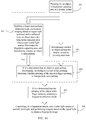
- FIG. 13 is a schematic flowchart of a fingerprint identification method according to an embodiment of the present application, which may be applied to an electronic device of an embodiment of the present application.
- the fingerprint identification method includes the following steps.
- the enabling the finger approaching detection mode includes: controlling, by a fingerprint sensor, the non-visible light source to actively emit light, where the fingerprint sensor drives the non-visible light source through a driving current, a light emitting period of the non-visible light source is a first period, a light emitting time of each period is a first light emitting time, and the driving current is a first driving current.
- the fingerprint sensor may control the non-visible light source to actively emit light, and in the finger approaching detection mode, instead of requiring a clear fingerprint image, whether a finger is approaching is required to be determined. Therefore, the fingerprint sensor may control the non-visible light source to periodically and intermittently emit light to detect whether a finger is approaching.
- the fingerprint sensor may drive the non-visible light source directly or indirectly through a driving signal, and the driving signal may be a driving voltage or a driving current.
- a light emitting period of the non-visible light source is a first period T1
- a light emitting time of each period is a first light emitting time t1
- the driving current is a first driving current 11.
- the if it is determined that the pressing of the object is the finger pressing, enabling the fingerprint detection mode includes: controlling, by the fingerprint sensor, the non-visible light source to actively emit light, where the fingerprint sensor drives the non-visible light source through a driving current, a light emitting period of the non-visible light source is a second period, a light emitting time of each period is a second light emitting time, and the driving current is a second driving current; and the second period is greater than the first period, the second light emitting time is greater than the first light emitting time, and the second driving current is greater than the first driving current.
- the fingerprint sensor may control the non-visible light source to actively emit light, a light emitting period of the non-visible light source is a second period T2, a light emitting time of each period is a second light emitting time t2, and a driving current is a second driving current 12, and T2>T1, t2>t1, I2>I1. Therefore, in the finger approaching detection mode, accuracy of finger approaching detection may be achieved, and power consumption may also be controlled at a lower level.
- FIGS. 14 to 16 show schematic flowcharts of fingerprint identification methods according to three embodiments of the present application. It should be understood that, compared with FIG. 13 , FIGS. 14 to 16 expand three different application scenarios, and the same content will not be repeatedly described herein.
- FIG. 14 is a flowchart of a fingerprint identification method using a single light source.
- the fingerprint identification method includes the following steps:
- the obtained fingerprint image may be matched with a previously stored authenticated fingerprint image, and if the matching succeeds, a further operation may be performed, which may be unlocking or other operations, which is not limited in this embodiment.
- FIG. 15 shows a flowchart of a fingerprint identification method using dual light sources and a single light emitting wave band.
- the fingerprint identification method includes the following steps:
- the first non-visible light source and the second non-visible light source may image the finger at different angles, and therefore a better imaging effect may be obtained in S307.
- FIG. 16 shows a flowchart of a fingerprint identification method using dual light sources and dual light emitting wave bands.
- the fingerprint identification method includes the following steps:
- the fingerprint sensor controls the non-visible light source to actively emit light, which may be referred to the content of FIG. 13 , and for the sake of brevity, it will not be repeatedly described herein.
- the embodiments shown in FIGS. 15 and 16 include two non-visible light sources; in the finger approaching detection mode, instead of requiring a clear fingerprint image, whether the finger is approaching is required to be determined, and one non-visible light source may be configured for approaching detection, or the two non-visible light sources may be configured for approaching detection simultaneously, which is not limited in this embodiment.
Landscapes
- Engineering & Computer Science (AREA)
- Multimedia (AREA)
- Physics & Mathematics (AREA)
- General Physics & Mathematics (AREA)
- Theoretical Computer Science (AREA)
- Human Computer Interaction (AREA)
- Signal Processing (AREA)
- Optics & Photonics (AREA)
- Image Input (AREA)
- Measurement Of The Respiration, Hearing Ability, Form, And Blood Characteristics Of Living Organisms (AREA)
Abstract
Description
- The present application relates to the field of information technologies, and in particular, to an optical fingerprint identification apparatus, an electronic device and a fingerprint identification method.
- With rapid development of science and technology, a fingerprint identification technology has been widely applied to various fields such as a mobile terminal, a smart home. At present, at the time of performing fingerprint identification, visible light with a certain wavelength is adopted to illuminate a biological feature, and a reflected light signal carrying biological feature information is transmitted to a sensor for capturing by utilizing a reflection imaging principle of visible light, and legitimacy of a user identity is confirmed by comparing the captured information with a biological feature registered and stored in advance.
- However, a fingerprint sensor can only passively receive a reflected visible light signal for fingerprint identification, thereby limiting flexible selection of a wavelength of excitation light used for imaging.
- Embodiments of the present application provides an optical fingerprint identification apparatus, an electronic device and a fingerprint identification method, which could flexibly select a wavelength of excitation light used for fingerprint identification, improve an ability to distinguish between real and fake fingers, and further improve safety of fingerprint identification.
- In a first aspect, provided is an optical fingerprint identification apparatus applied to an electronic device having a display screen, including: at least one non-visible light source, configured to emit non-visible light to a human finger to provide excitation light for fingerprint identification, where a number of light emitting wave bands of the non-visible light source is at least 1; an optical component, disposed under a fingerprint detecting area of the display screen, and configured to receive signal light scattered and reflected by the human finger and collimate and/or converge the signal light; and a fingerprint sensor, disposed under the optical component, and configured to perform imaging based on the signal light passing through the optical component, where a working wave band of the fingerprint sensor is the same as a light emitting wave band of the non-visible light source, a number of the working wave bands is the same as the number of the light emitting wave bands, and the fingerprint sensor is directly or indirectly electrically connected to the non-visible light source, and is configured to control the non-visible light source to actively emit light.
- In one possible implementation manner, the optical fingerprint identification apparatus further includes a filter disposed between the optical component and the fingerprint sensor, and a light passing wave band of the filter is the same as the light emitting wave band of the non-visible light source.
- In one possible implementation manner, a number of the non-visible light sources is greater than 1, the number of the light emitting wave bands of the non-visible light source is greater than or equal to 1, a number of light passing wave bands of the filter is equal to the number of light emitting wave bands of the non-visible light source, and the light emitting wave bands are in one-to-one correspondence with the light passing wave bands.
- In one possible implementation manner, the electronic device includes a cover glass, and the display screen and the non-visible light source are disposed side by side under the cover glass.
- In one possible implementation manner, the non-visible light source is disposed on at least one side of a universal serial bus USB interface of the electronic device.
- In one possible implementation manner, the display screen is an organic light-emitting diode OLED display screen.
- In one possible implementation manner, the display screen includes a display module and a backlight module, and the backlight module is capable of transmitting the non-visible light emitted by the non-visible light source.
- In one possible implementation manner, the optical component includes a collimator array, and the collimator array includes a plurality of collimating holes configured to collimate the signal light and direct the signal light to the fingerprint sensor.
- In one possible implementation manner, the optical component includes: at least one lens and a support; the lens is configured to converge the signal light and direct the signal light to the fingerprint sensor; and the support is configured to accommodate and fix the lens.
- In a possible implementation manner, the optical component includes at least one camera lens, a lens barrel and a lens holder; the camera lens is configured to converge the signal light and direct the signal light to the fingerprint sensor; the lens barrel is configured to accommodate the camera lens; and the lens holder is configured to fix the lens barrel.
- In one possible implementation manner, the lens barrel and the lens holder are of an integrated structure.
- In one possible implementation manner, the lens barrel and the lens holder are of a separate structure, and the lens barrel and the lens holder are fixed through threaded connection.
- In one possible implementation manner, the optical component includes a microlens array and a diaphragm array disposed under the microlens array; the microlens array includes a plurality of microlenses configured to converge the signal light; the diaphragm array includes a plurality of diaphragms, where the diaphragms are in one-to-one correspondence with the microlenses, and the diaphragms are configured to direct the signal light converged by the microlens to the fingerprint sensor.
- In one possible implementation manner, the fingerprint sensor includes a driving interface electrically connected to the non-visible light source, and is configured to directly control the non-visible light source to actively emit light.
- In one possible implementation manner, the optical fingerprint identification apparatus further includes a control module, and the fingerprint sensor is electrically connected to the non-visible light source through the control module; the fingerprint sensor is communicatively connected to the control module, and a driving interface of the control module is electrically connected to the non-visible light source; and the fingerprint sensor is configured to indirectly control the non-visible light source to actively emit light through the control module.
- In one possible implementation manner, the optical fingerprint identification apparatus includes two operating modes of a finger approaching detection mode and a fingerprint detection mode.
- In one possible implementation manner, in the finger approaching detection mode, the fingerprint sensor controls the non-visible light source to periodically and intermittently emit light, a light emitting period is a first period, a light emitting time of each period is a first light emitting time, a driving current output by the driving interface is a first driving current, and the first driving current is configured to drive the non-visible light source to actively emit light.
- In one possible implementation manner, in the fingerprint detection mode, the fingerprint sensor controls the non-visible light source to periodically and intermittently emit light, a light emitting period of the non-visible light source is a second period, a light emitting time of each period is a second light emitting time, a driving current output by the driving interface is a second driving current, and the second driving current is configured to drive the non-visible light source to actively emit light; and the second period is greater than the first period, the second light emitting time is greater than the first light emitting time, and the second driving current is greater than the first driving current.
- In one possible implementation manner, the fingerprint sensor includes a plurality of pixel units, and in the finger approaching detection mode, part of the pixel units perform imaging based on the signal light; and in the fingerprint detection mode, all of the pixel units perform imaging based on the signal light.
- In a second aspect, provided is an electronic device including a display screen configured to display a picture and detect presence of a contact input and the optical fingerprint identification apparatus in the first aspect or any possible implementation manner of the first aspect.
- In a third aspect, provided is a fingerprint identification method applied to the electronic device of the second aspect, and the fingerprint identification method includes: enabling a finger approaching detection mode, performing imaging based on signal light scattered and/or reflected from an object above a fingerprint capturing area when a non-visible light source illuminates the fingerprint capturing area, and determining whether an object is approaching; determining whether an object presses a display screen by pressing detection; if it is determined that an object is approaching, determining, according to a result of the pressing detection, whether pressing of the object is finger pressing or foreign body mistouching; if it is determined that the pressing of the object is the finger pressing, enabling a fingerprint detection mode, and performing imaging based on the signal light to obtain a fingerprint image.
- In one possible implementation manner, the enabling the finger approaching detection mode includes: controlling, by a fingerprint sensor, the non-visible light source to actively emit light, where the fingerprint sensor drives the non-visible light source through a driving current, a light emitting period of the non-visible light source is a first period, a light emitting time of each period is a first light emitting time, and the driving current is a first driving current.
- In one possible implementation manner, the if it is determined that the pressing of the object is the finger pressing, enabling the fingerprint detection mode includes: controlling, by the fingerprint sensor, the non-visible light source to actively emit light, the fingerprint sensor drives the non-visible light source through a driving current, a light emitting period of the non-visible light source is a second period, a light emitting time of each period is a second light emitting time, and the driving current is a second driving current; and the second period is greater than the first period, the second light emitting time is greater than the first light emitting time, and the second driving current is greater than the first driving current.
- Based on the foregoing technical solution, a wavelength of excitation light used for fingerprint identification could be flexibly selected, an ability to distinguish between real and fake fingers is improved, and safety of fingerprint identification is further improved.
-
-
FIG. 1 is a schematic structural diagram of an under-screen fingerprint identification apparatus. -
FIG. 2 is a schematic structural diagram of an optical fingerprint identification apparatus according to an embodiment of the present application. -
FIG. 3 is a schematic diagram of an optical fingerprint identification apparatus performing fingerprint identification according to the embodiment of the present application. -
FIG. 4 is a schematic diagram of another optical fingerprint identification apparatus performing fingerprint identification according to an embodiment of the present application. -
FIG. 5 is a schematic diagram of an internal connection relationship of an optical fingerprint identification apparatus according to an embodiment of the present application. -
FIG. 6 is a schematic diagram of an internal connection relationship of another optical fingerprint identification apparatus according to an embodiment of the present application. -
FIG. 7 is a schematic diagram of a positional relationship of an optical fingerprint identification apparatus applied to an electronic device according to an embodiment of the present application. -
FIGS. 8 to 10 are transmittance of a filter of an optical fingerprint identification apparatus for non-visible light sources with different wavelengths according to an embodiment of the present application. -
FIG. 11 is a schematic diagram of working states of an optical fingerprint identification apparatus in a finger approaching detection mode and a fingerprint identification mode according to an embodiment of the present application. -
FIG. 12 is a schematic diagram of working of pixel units of a fingerprint sensor of an optical fingerprint identification apparatus in a finger approaching detection mode and a fingerprint identification mode according to an embodiment of the present application. -
FIG. 13 is a schematic flowchart of a fingerprint identification method according to an embodiment of the present application. -
FIG. 14 is an exemplary flowchart of a fingerprint identification method according to an embodiment of the present application. -
FIG. 15 is an exemplary flowchart of another fingerprint identification method according to an embodiment of the present application. -
FIG. 16 is an exemplary flowchart of yet another fingerprint identification method according to an embodiment of the present application. - Technical solutions in embodiments of the present application will be described hereinafter in conjunction with the accompanying drawings.
- It should be understood that technical solutions of embodiments of the present application may be applied to various electronic devices, for example, a portable or mobile computing device such as a smart phone, a notebook computer, a tablet computer and a game device, and other electronic devices such as an electronic database, an automobile and an automated teller machine (Automated Teller Machine, ATM), which is not limited in the embodiments of the present application.
- As a common application scenario, an optical fingerprint identification apparatus provided in an embodiment of the present application may be applied to a smart phone, a tablet computer, and other electronic devices with a display screen or other electronic devices; More specifically, in the foregoing electronic device, the optical fingerprint identification apparatus may be disposed in a partial area or an entire area under a display screen, thereby forming an under-display (Under-display or Under-screen) optical fingerprint system.
-
FIG. 1 is a schematic structural diagram of an under-screen fingerprint identification apparatus. As shown inFIG. 1 , adisplay screen 150 may be an organic light-emitting diode (Organic Light-Emitting Diode, OLED) display screen, visible light emitted by a light emitting unit of the OLED display screen is configured to provide excitation light for fingerprint identification; when a finger is pressed against a fingerprint detecting area (not shown inFIG. 1 ) of thedisplay screen 150, the excitation light is reflected by the finger and reaches an area under thedisplay screen 150; and at this time, the reflected excitation light carries fingerprint information of the finger and becomes signal light. The signal light continues to be transmitted downward to reach anoptical component 120; optionally, theoptical component 120 may include alens 121 configured to converge the signal light reflected by the finger to aphotosensitive area 131 of afingerprint sensor 130 to capture a fingerprint image. A lower part ofFIG. 1 is a top view of thefingerprint sensor 130. - Optionally, a
filter 140 may also be disposed between theoptical component 120 and thefingerprint sensor 130, and thefilter 140 is configured to filter stray light to obtain a better imaging effect. - In an existing optical fingerprint identification apparatus, the
fingerprint sensor 140 may only passively receive visible light emitted by the OLED display screen, thus limiting flexible selection of a wavelength of excitation light used for imaging. The optical fingerprint identification apparatus provided in the embodiment of the present application may flexibly select the wavelength of the excitation light used for imaging, improve an ability to distinguish between real and fake fingers, and further improve safety of fingerprint identification. -
FIG. 2 is a schematic structural diagram of an optical fingerprint identification apparatus according to an embodiment of the present application. An optical fingerprint identification apparatus 200 may be applied to an electronic device having a display screen, and includes at least onenon-visible light source 210, anoptical component 220, and afingerprint sensor 230. - The
non-visible light source 210 emits non-visible light to a human finger to provide excitation light for fingerprint identification, and the number of light emitting wave bands of thenon-visible light source 210 is at least 1. The optical fingerprint identification apparatus 200 may include the at least onenon-visible light source 210, and if the number ofnon-visible light sources 210 is greater than 1, the number of light emitting wave bands of thenon-visible light sources 210 is greater than or equal to 1, for example, when the optical fingerprint identification apparatus 200 includes twonon-visible light sources 210, wavelengths of the twonon-visible light sources 210 may be 850 nm and 940 nm, respectively, or may be both 850 nm, or may be both 940 nm. The number ofnon-visible light sources 210 and the number of light emitting wave bands are not limited in the embodiment of the present application, and are set according to requirements of an actual product. - It should be understood that when a plurality of
non-visible light sources 210 adopt a same light emitting wave band, it has advantages of having high illumination intensity, obtaining stronger signal light for fingerprint detection, and acquiring a better fingerprint imaging effect; also when the plurality ofnon-visible light sources 210 are located in different positions, the finger may be imaged at different angles, and the fingerprint imaging effect may also be improved; and when the plurality ofnon-visible light sources 210 adopt different light emitting wave bands, in addition to increasing the illumination intensity, the finger may be imaged in different wave bands to obtain different imaging features. Specifically, different objects have different transmittance for light with different wavelengths; for example, a finger has lower transmittance for light with a wavelength of 850 nm than that of light with a wavelength of 940 nm, and a fake finger and other foreign objects have relatively close transmittance for the foregoing light with the two wavelengths; therefore, when fingerprint imaging is performed, data of the real finger and data of the fake finger or other foreign objects will differ significantly; and this feature may be used to distinguish between the real finger and the fake finger and foreign object, improve an interception rate of fake finger attacks, that is, to improve the ability to distinguish between the real finger and the fake finger, and further improve security of fingerprint identification. In other words, by increasing the number of light emitting wave bands of the non-visiblelight source 210, difference characteristic data of transmittance of different objects for light with different wavelengths is increased, thereby improving the ability of the optical fingerprint identification apparatus to distinguish between the real finger and the fake finger and foreign object. - The
optical component 220 is disposed under a fingerprint detecting area of the display screen, is configured to receive signal light scattered and reflected by the human finger, and collimate or converge the signal light. Theoptical component 220 has higher transmittance for the non-visible light emitted by the non-visiblelight source 210. As an optional embodiment, theoptical component 220 may include a collimator array, and the collimator array includes a plurality of collimating holes configured to collimate the signal light and direct the signal light to thefingerprint sensor 230. - As another optional embodiment, the
optical component 220 may include at least one lens and a holder. The lens is configured to converge the signal light and direct the signal light to thefingerprint sensor 230; the lens may increase an incident angle of a central field of view, increase convergence of the signal light and obtain a better imaging effect. It should be understood that the number of lenses may be multiple, so that a better convergence effect may be obtained, and at the same time, the lens may be a spherical lens or an aspheric lens, or a combination of a spherical lens and an aspheric lens, which is not limited in this embodiment. The support is configured to accommodate and fix the lens. - As another optional embodiment, the
optical component 220 may include at least one camera lens, a lens barrel and a lens holder; the camera lens is configured to converge the signal light and direct the signal light to thefingerprint sensor 230; the lens barrel is configured to accommodate the camera lens; and the lens holder is configured to fix the lens barrel. Optionally, the lens barrel and the lens holder may be of an integrated structure, or the lens barrel and the lens holder may be of a separate structure, and the lens barrel and the lens holder are fixed through threaded connection. - As another optional embodiment, the
optical component 220 may include a microlens array and a diaphragm array disposed under the microlens array; the microlens array includes a plurality of microlenses configured to converge the signal light; the diaphragm array includes a plurality of diaphragms, where the diaphragms are in one-to-one correspondence with the microlenses, and the diaphragms are configured to direct the signal light converged by the microlens to thefingerprint sensor 230. - The
fingerprint sensor 230 is disposed under theoptical component 220, and is configured to perform imaging based on the signal light passing through theoptical component 220, where a working wave band of thefingerprint sensor 230 is the same as the light emitting wave band of the non-visiblelight source 210, the number of working wave bands is the same as the number of light emitting wave bands, and thefingerprint sensor 230 is directly or indirectly electrically connected to the non-visiblelight source 210, and is configured to control the non-visiblelight source 210 to actively emit light. - It should be understood that when the optical fingerprint identification apparatus 200 includes more than one non-visible
light source 210 and the number of light emitting wave bands of the non-visiblelight source 210 is greater than 1, the number of working wave bands of thefingerprint sensor 230 is the same as the number of light emitting wave bands, and is also greater than 1, that is, there may be multiple working wave bands of thefingerprint sensor 230. For example, when the optical fingerprint identification apparatus 200 includes two non-visiblelight sources 210, wavelengths of the two non-visiblelight sources 210 may be 850 nm and 940 nm, respectively, the number of working wave bands of thefingerprint sensor 230 is the same as the number of light emitting wave bands of the non-visiblelight sources 210, and there are also two wave bands, which are 850 nm and 940 nm, respectively, thefingerprint sensor 230 is not sensitive to light of other wave bands except 850 nm and 940 nm, and thus an influence of light of other wave bands on a fingerprint imaging effect may be reduced. - The
fingerprint sensor 230 is directly or indirectly electrically connected to the non-visible light source 210 (not shown inFIG. 2 ), and is configured to control the non-visiblelight source 210 to actively emit light, which may be referred toFIGS. 5 and 6 , and this embodiment will not be described in detail. -
FIG. 3 is a schematic diagram of an optical fingerprint identification apparatus performing fingerprint identification according to an embodiment of the present application, that is, it is a schematic diagram of the optical fingerprint identification apparatus 200 shown inFIG. 2 applied to an electronic device performing fingerprint identification. As shown inFIG. 3 , a fingerprint identification apparatus includes a non-visiblelight source 310, anoptical component 320, and afingerprint sensor 330, which have been described in detail inFIG. 2 and will not be repeatedly described herein. - An electronic device may include a
cover glass 360 for protecting adisplay screen 350, and thedisplay screen 350 and the non-visiblelight source 310 may be disposed side by side under thecover glass 360. It should be understood that in order to prevent a user from seeing the non-visiblelight source 310 disposed under the cover glass through thecover glass 360, a layer of an isolation film (not shown inFIG. 3 ) may be disposed between thecover glass 360 and the non-visiblelight source 310, the isolation film may block visible light and has higher transmittance for the non-visible light emitted by the non-visiblelight source 310. - The
optical component 320 may be disposed under thedisplay screen 350, specifically, may be located under a fingerprint detecting area (not shown inFIG. 3 ) of thedisplay screen 350, and the fingerprint detecting area is located in part or all of a display area of the display screen. Thefingerprint sensor 330 may be disposed under theoptical component 320. Theoptical component 320 shown in this embodiment includes alens 321 and asupport 322. Thelens 321 is configured to converge the signal light and direct the signal light to thefingerprint sensor 330; and thelens 321 may increase an incident angle of a central field of view, increase convergence of the signal light, and obtain a better imaging effect. It should be understood that the number oflenses 321 may be multiple, so that a better convergence effect may be obtained, and at the same time, thelens 321 may be a spherical lens or an aspheric lens, or a combination of a spherical lens and an aspheric lens, which is not limited in this embodiment. Thesupport 322 is configured to accommodate and fix thelens 321. Theoptical component 320 in the optical fingerprint identification apparatus shown inFIG. 3 is merely illustrative, and theoptical component 320 may also be an optical component including a collimator array, or an optical component including at least one camera lens, a lens barrel and a lens holder. Reference is made to the contents described inFIG. 2 , which will not be repeatedly described herein. - A basic process of performing fingerprint identification by the optical fingerprint identification apparatus in this embodiment is as follows: the non-visible light emitted by the non-visible
light source 310 is incident on the interior of a human finger pressed on thecover glass 360 through thecover glass 360, is scattered by tissues in the finger or is reflected by a finger surface, and then sequentially passes through thecover glass 360, thedisplay screen 350 and theoptical component 320, to reach thefingerprint sensor 330; and the scattered and/or reflected non-visible light carries fingerprint information of the finger to become the signal light, and thefingerprint sensor 330 is configured to perform imaging based on the signal light. Thefingerprint sensor 330 may include aphotosensitive area 331 which may include a plurality of pixel units. Therefore, thefingerprint sensor 330 is configured to perform imaging based on the signal light, which actually refers that thephotosensitive area 331 of thefingerprint sensor 330 is configured to perform imaging based on the signal light. - The optical fingerprint identification apparatus may also include a
filter 340 which may be disposed in a light path between thedisplay screen 350 and thefingerprint sensor 330. As an optional embodiment, thefilter 340 is disposed between theoptical component 320 and thefingerprint sensor 330, and a light passing wave band of thefilter 340 is the same as a light emitting wave band of the non-visiblelight source 310, and therefore thefilter 340 can filter stray light and reduce interference of stray light in fingerprint identification. For example, a film may be coated on a surface of thefingerprint sensor 330 by a vapor deposition process to form thefilter 340, and other components may be used to fix thefilter 340 between theoptical component 320 and thefingerprint sensor 330, which is not limited in this embodiment and may be set according to an actual product requirement. - When the number of non-visible
light sources 310 is greater than 1, the number of light emitting wave bands of the non-visiblelight sources 310 is greater than or equal to 1, the number of light passing wave bands of thefilter 340 is equal to the number of light emitting wave bands of the non-visiblelight source 310, and the light emitting wave bands is in one-to-one correspondence with the light passing wave band. It should be understood that when the fingerprint identification apparatus includes more than one non-visiblelight source 310 and the number of light emitting wave bands of the non-visiblelight source 310 is greater than 1, the number of light passing wave bands of thefilter 340 is the same as the number of light emitting wave bands, and is also greater than 1, that is, there may be multiple light passing wave bands of thefilter 340. For example, when the fingerprint identification apparatus includes two non-visiblelight sources 310, wavelengths of the two non-visiblelight sources 310 may be 850 nm and 940 nm, respectively, the number of light passing wave bands of thefilter 340 is the same as the number of light emitting wave bands of the non-visiblelight sources 310, and there are two wave bands, which are 850 nm and 940 nm, respectively. - In the embodiment of the present application, the
display screen 350 may be an OLED display screen. Here, the non-visiblelight source 310 in the optical fingerprint identification apparatus rather than visible light emitted by the OLED display screen is used as excitation light for fingerprint identification, which has advantages of flexibly selecting a wavelength of the excitation light for fingerprint identification, improving the ability to distinguish between real and fake fingers, and further improving safety of fingerprint identification. As another optional embodiment, the optical fingerprint identification apparatus may also be applied to an electronic device having other types of display screen, for example, the display screen may include a display module and a backlight module, the backlight module is configured to provide a visible light source to make a display module display a picture, as shown inFIG. 4 . - As shown in
FIG. 4 , adisplay screen 450 includes adisplay module 451 and abacklight module 452. Optionally, thedisplay module 451 may be a liquid crystal module and thedisplay screen 450 may be a liquid crystal display screen. An existing backlight module generally includes a point light source and a plurality of layers of laminated materials with different functions, and the laminated material includes a reflective film (also referred to as a mirror film), a light directing plate, a light homogenizing film (also referred to as a diffusion film) and a prism film (also referred to as a brightness enhancement film), and there are at least one layer of the light homogenizing film and at least one layer of the prism film. A purpose of combining these laminated materials is to make one or more point light sources form a surface light source, and also to improve a light extraction rate, so that a picture displayed on the liquid crystal display screen could appear uniform in brightness. As the reflective film reflects light, other remaining laminated materials such as the light directing plate, the light homogenizing film and the prism film would disperse the light, especially the light homogenizing film would play a nebulizing role, and the whole backlight module is considered to be opaque. Therefore, it is necessary to modify the backlight module so that it can transmit the non-visible light emitted by a non-visiblelight source 410, thereby implementing fingerprint identification. Thebacklight module 452 is a modified module of the existing backlight module, which has higher transmittance for the non-visible light emitted by the non-visiblelight source 410, and thus under-screen optical fingerprint detection may be performed. - As shown in
FIG. 4 , thedisplay screen 450 and the non-visiblelight source 410 are disposed side by side under acover glass 460, and anoptical component 420 is disposed under the fingerprint detecting area (not shown inFIG. 4 ) of thedisplay screen 450. Theoptical component 420 includes alens 421 and asupport 422. Afingerprint sensor 430 is disposed under theoptical component 420, and aphotosensitive area 431 of thefingerprint sensor 430 is configured to image received signal light. The optical fingerprint identification apparatus may further include afilter 440, and as an optional embodiment, thefilter 440 may be disposed between theoptical component 420 and thefingerprint sensor 430. Other features besides the display screen inFIG. 4 may also be referred to the content ofFIG. 3 , which will not be repeatedly described herein. It should be understood that the optical fingerprint identification apparatus shown inFIGS. 3 and4 is merely illustrative and should not be construed as a limitation on the optical fingerprint identification apparatus of the present application. -
FIGS. 5 and 6 are schematic diagrams of internal connection relationships of two optical fingerprint identification apparatuses according to embodiments of the present application. It should be understood thatFIGS. 5 and 6 are applicable to the optical fingerprint identification apparatus shown inFIGS. 2 to 4 , and for the sake of brevity, the same contents as those inFIGS. 2 to 4 will not be repeatedly described herein. - As shown in
FIG. 5 , afingerprint sensor 530 is directly connected to a non-visiblelight source 510. Optionally, thefingerprint sensor 530 includes a drivinginterface 532, through which thefingerprint sensor 530 outputs a driving signal, and the driving signal may be a driving current or a driving voltage, thefingerprint sensor 530 is configured to directly control the non-visiblelight source 510 to actively emit light, that is, thefingerprint sensor 530 controls the non-visiblelight source 510 to emit light through the output driving signal. - A
display screen 550 of an electronic device may display a picture, and optionally, thedisplay screen 550 may also detect presence of a touch input, for example, a touch or pressing operation of a user's finger can be detected, so as to provide a human-computer interaction interface for the user, that is, thedisplay screen 550 may be a touch display screen with a touch function. For example, in an embodiment, the electronic device may include a touch sensor, and the touch sensor may be specifically a touch panel (Touch Panel, TP), which may be disposed on a surface of thedisplay screen 550, or may be partially integrated or entirely integrated into an interior of thedisplay screen 550 to form the touch display screen. - As an optional embodiment, both the
fingerprint sensor 530 and thedisplay screen 550 may be communicatively connected to a main control unit 570 of the electronic device, and both may respond to a command of the main control unit 570 and transmit data. - As shown in
FIG. 6 , an optical fingerprint identification apparatus further includes acontrol module 633, through which afingerprint sensor 630 is electrically connected to a non-visiblelight source 610. Thefingerprint sensor 630 is communicatively connected to thecontrol module 633 to transmit data. - Optionally, the
control module 633 includes a drivinginterface 632, through which thecontrol module 633 outputs a driving signal, and the driving signal may be a driving current or a driving voltage; thefingerprint sensor 530 is configured to indirectly control the non-visiblelight source 610 to actively emit light through thecontrol module 633, that is, thefingerprint sensor 530 indirectly controls the non-visiblelight source 610 to emit light through the driving signal output by thecontrol module 633. - A
display screen 650 inFIG. 6 is similar to thedisplay screen 550, and may be a touch display screen, which will not be repeatedly described herein. As an optional embodiment, both thecontrol unit 633 and thedisplay screen 650 may be communicatively connected to amain control unit 670 of an electronic device, and both may respond to a command of themain control unit 670 and transmit data. -
FIG. 7 is a schematic diagram of a positional relationship of an optical fingerprint identification apparatus applied to an electronic device according to an embodiment of the present application.FIG. 7 does not show an entire structure of an optical fingerprint identification apparatus, and the entire structure thereof may be understood with reference toFIG. 3 . As shown inFIG. 3 , theoptical component 320, thefingerprint sensor 330, and thefilter 340 may all be disposed under the fingerprint detecting area of thedisplay screen 350 of the electronic device, that is, under afingerprint detecting area 751 of adisplay screen 750 inFIG. 7 . Considering that a universal serial bus (Universal Serial Bus, USB) interface is generally disposed at a central position of a lower area of an electronic device, the USB interface may be connected to a charger to charge the electronic device or the USB interface may be used as an earphone jack to connect headphones. - Optionally, the non-visible light source may be disposed on at least one side of the USB interface of the electronic device.
FIG. 7 shows three embodiments in sequence, and from left to right, a first embodiment is that a non-visiblelight source 711 is disposed on a left side of the USB interface; a second embodiment is that a non-visiblelight source 711 and a non-visiblelight source 712 are respectively disposed on a left side and a right side of the USB interface, and light emitting wave bands of the non-visiblelight source 711 and the non-visiblelight source 712 may be the same or different, which is not limited in this embodiment; different from the second embodiment, in a third embodiment the number of non-visiblelight sources 711 and non-visiblelight sources 712 may be greater than 1, respectively, and in this embodiment, two non-visiblelight sources 711 are disposed on a left side of the USB interface and two non-visiblelight sources 712 are disposed on a right side of the USB interface. The embodiment shown inFIG. 7 is merely exemplary and should not be taken as a limitation on the present application. Optionally, thedisplay screen 750 and the non-visible light source may be disposed side by side under the cover glass. -
FIGS. 8 to 10 are schematic diagrams of transmittance of a filter of an optical fingerprint identification apparatus to non-visible light sources with different wavelengths according to an embodiment of the present application. The number of light passing wave bands of a filter may be greater than 1, and be equal to the number of light emitting wave bands of a non-visible light source. As shown inFIG. 8 , the filter may pass through non-visible light of two wave bands at the same time, and the number of light passing wave bands is 2, that is, the filter has higher transmittance for non-visible light of the two wave bands; and reference is made to the second embodiment or the third embodiment ofFIG. 7 , for example, the light emitting wave band of the non-visiblelight source 711 may be 850 nm, and the light emitting wave band of the non-visiblelight source 712 may be 940 nm. The light passing wave bands of the filter are 850 nm and 940 nm, and therefore the filter has higher transmittance for the non-visiblelight source 711 and the non-visiblelight source 712. - As shown in
FIG. 9 andFIG. 10 , the filter may only pass through non-visible light of one wave band, and the number of light passing wave bands is 1, that is, the filter only has higher transmittance for non-visible light of one wave band, and reference may also be made to the second embodiment or the third embodiment ofFIG. 7 , for example, the light emitting wave bands of the non-visiblelight source 711 and the non-visiblelight source 712 may both be 850 nm, and the light passing wave band of the filter is 850 nm. Alternatively, the light emitting wave bands of the non-visiblelight source 711 and the non-visiblelight source 712 may both be 940 nm, and correspondingly the light passing wave band of the filter is 940 nm. The embodiment of the present application does not limit the number and wave band of light passing wave bands of the filter, as long as it corresponds to the number and wave band of light emitting wave bands of the non-visible light source. The filter is configured to filter stray light to improve the imaging effect of fingerprint identification. -
FIG. 11 is a schematic diagram of working states of an optical fingerprint identification apparatus in a finger approaching detection mode and a fingerprint detection mode according to an embodiment of the present application. An optical fingerprint identification apparatus of an embodiment of the present application includes two working modes of a finger approaching detection mode and a fingerprint detection mode, and the optical fingerprint identification apparatus may implement switching of the two modes. A fingerprint sensor is directly or indirectly electrically connected to a non-visible light source and is configured to control the non-visible light source to actively emit light. - In the finger approaching detection mode, instead of requiring a clear fingerprint image, whether the finger is approaching is required to be determined. Therefore, the fingerprint sensor may control the non-visible light source to periodically and intermittently emit light to detect whether a finger is approaching.
- Optionally, the fingerprint sensor may directly output a driving signal to drive the non-visible light source to emit light, for example, as shown in
FIG. 5 , thefingerprint sensor 530 outputs the driving signal through the drivinginterface 532 to drive the non-visiblelight source 510 to actively emit light. - Optionally, the fingerprint sensor may indirectly output the driving signal to drive the non-visible light source to actively emit light through other components such as a control module, for example, as shown in
FIG. 6 , thecontrol module 633 outputs the driving signal through the drivinginterface 632 to drive the non-visiblelight source 610 to actively emit light, that is, thefingerprint sensor 630 indirectly controls the non-visiblelight source 610 to actively emit light through thecontrol module 633. - As an optional embodiment, the driving signal may be a driving current; in the finger approaching detection mode, a light emitting period of the non-visible light source is a first period T1, a light emitting time of each period is a first light emitting time t1, and a driving current is a first driving current 11. Moreover, in the finger approaching detection mode, as shown in a left diagram in
FIG. 12 , only part of pixel units of the fingerprint sensor may be turned on for detection, and part of the pixel units perform imaging based on the signal light. Similarly, since in a finger approaching detection mode, instead of requiring a clear fingerprint image, whether the finger is approaching is required to be determined, and only part of pixel units are turned on for detection, accuracy of the finger approaching detection is not be affected, and power consumption of the fingerprint sensor may be reduced. - Different from the finger approaching detection mode, in a fingerprint detection mode, when the fingerprint sensor controls the non-visible light source to periodically and intermittently emit light, a light emitting period of the non-visible light source is a second period T2, a light emitting time of each period is a second light emitting time t2, and a driving current is a second driving current 12, and T2>T1, t2>t1, I2>I1. In the finger approaching detection mode, the non-visible light source has a smaller driving current and a shorter light emitting time, and therefore power consumption thereof may also be controlled at a relatively low level. In the fingerprint detection mode, as shown in a right diagram in
FIG. 12 , all pixel units of the fingerprint sensor may be turned on, and all of the pixel units perform imaging based on the signal light, to ensure the accuracy of fingerprint detection. - It should be understood that the plurality of pixel units of the fingerprint sensor shown in
FIG. 12 are the photosensitive area of the fingerprint sensor. - Through the finger approaching detection mode, with the pressing detection of a display screen having a touch function, whether the finger performs pressing may be determined more accurately and the fingerprint detection mode is enabled, so that not only can mistouching events be reduced, but also camouflage of some non-transparent fake fingerprints may be intercepted, thereby implementing living body fingerprint identification.
- An embodiment of the present application also provides an electronic device including a display screen and an optical fingerprint identification apparatus of the embodiment of the present application, and the display screen is configured to display a picture and detect presence of a contact input. By way of example and not limitation, the electronic device may be a terminal device, a mobile phone, a tablet computer, a notebook computer, a desktop computer, a vehicle-mounted electronic device, and a wearable smart device, or the like. The wearable smart device includes a full functioned and large sized device that may implement complete or partial functions without relying on a smart phone such as a smart watch, a smart glass or the like, and a device that is only focused on certain application functions and needs to be used in conjunction with a smart phone or other devices such as various smart bracelets and smart jewelry for physical sign monitoring.
-
FIG. 13 is a schematic flowchart of a fingerprint identification method according to an embodiment of the present application, which may be applied to an electronic device of an embodiment of the present application. - As shown in
FIG. 13 , the fingerprint identification method includes the following steps. - S101, enabling a finger approaching detection mode, performing imaging based on signal light scattered and/or reflected from an object above a fingerprint capturing area when a non-visible light source illuminates the fingerprint capturing area, and determining whether an object is approaching;
- S102, determining whether an object presses a display screen by pressing detection;
- S103, if it is determined that an object is approaching, determining, according to a result of the pressing detection, whether pressing of the object is finger pressing or foreign body mistouching; and
- S104, if it is determined that the pressing of the object is the finger pressing, enabling a fingerprint detection mode, and performing imaging based on the signal light to obtain a fingerprint image.
- In S101, the enabling the finger approaching detection mode includes: controlling, by a fingerprint sensor, the non-visible light source to actively emit light, where the fingerprint sensor drives the non-visible light source through a driving current, a light emitting period of the non-visible light source is a first period, a light emitting time of each period is a first light emitting time, and the driving current is a first driving current.
- In the finger approaching detection mode, the fingerprint sensor may control the non-visible light source to actively emit light, and in the finger approaching detection mode, instead of requiring a clear fingerprint image, whether a finger is approaching is required to be determined. Therefore, the fingerprint sensor may control the non-visible light source to periodically and intermittently emit light to detect whether a finger is approaching. Optionally, the fingerprint sensor may drive the non-visible light source directly or indirectly through a driving signal, and the driving signal may be a driving voltage or a driving current. Reference is specifically made to
FIG. 11 . For example, a light emitting period of the non-visible light source is a first period T1, a light emitting time of each period is a first light emitting time t1, and the driving current is a first driving current 11. - In S104, the if it is determined that the pressing of the object is the finger pressing, enabling the fingerprint detection mode includes: controlling, by the fingerprint sensor, the non-visible light source to actively emit light, where the fingerprint sensor drives the non-visible light source through a driving current, a light emitting period of the non-visible light source is a second period, a light emitting time of each period is a second light emitting time, and the driving current is a second driving current; and the second period is greater than the first period, the second light emitting time is greater than the first light emitting time, and the second driving current is greater than the first driving current.
- In the fingerprint detection mode, the fingerprint sensor may control the non-visible light source to actively emit light, a light emitting period of the non-visible light source is a second period T2, a light emitting time of each period is a second light emitting time t2, and a driving current is a second driving current 12, and T2>T1, t2>t1, I2>I1. Therefore, in the finger approaching detection mode, accuracy of finger approaching detection may be achieved, and power consumption may also be controlled at a lower level.
-
FIGS. 14 to 16 show schematic flowcharts of fingerprint identification methods according to three embodiments of the present application. It should be understood that, compared withFIG. 13 ,FIGS. 14 to 16 expand three different application scenarios, and the same content will not be repeatedly described herein. -
FIG. 14 is a flowchart of a fingerprint identification method using a single light source. The fingerprint identification method includes the following steps: - S201, pressing, by an object, a fingerprint capturing area of a display screen;
- S202, enabling a finger approaching detection mode, performing imaging based on signal light scattered and/or reflected from an object above the fingerprint capturing area when a non-visible light source illuminates the fingerprint capturing area, and determining whether an object is approaching;
- S203, determining whether an object presses the display screen by pressing detection;
- S204, if it is determined that an object is approaching, determining, according to a result of the pressing detection, whether pressing of the object is finger pressing or foreign body mistouching;
- S205, if it is determined that the pressing of the object is the finger pressing, enabling a fingerprint detection mode; and
- S206, controlling, by a fingerprint sensor, non-visible light source to actively emit light, and performing imaging based on the signal light to obtain a fingerprint image.
- In S206, the obtained fingerprint image may be matched with a previously stored authenticated fingerprint image, and if the matching succeeds, a further operation may be performed, which may be unlocking or other operations, which is not limited in this embodiment.
- In
FIG. 15 , two non-visible light sources are taken as an example, and in actual application, more than two non-visible light sources may be selected for fingerprint identification according to an actual application scenario.FIG. 15 shows a flowchart of a fingerprint identification method using dual light sources and a single light emitting wave band. The fingerprint identification method includes the following steps: - S301, pressing, by an object, a fingerprint capturing area of a display screen;
- S302, enabling a finger approaching detection mode, performing imaging based on signal light scattered and/or reflected from an object above the fingerprint capturing area when a non-visible light source illuminates the fingerprint capturing area, and determining whether an object is approaching;
- S303, determining whether an object presses the display screen by pressing detection;
- S304, if it is determined that an object is approaching, determining, according to a result of the pressing detection, whether pressing of the object is finger pressing or foreign body mistouching;
- S305, if it is determined that the pressing of the object is the finger pressing, enabling a fingerprint detection mode; and
- S306, controlling, by a fingerprint sensor, a first non-visible light source with a light emitting wave band of λ1 to actively emit light, and performing imaging based on the non-visible light emitted by the first non-visible light source scattered and/or reflected by the finger, to obtain a first fingerprint image;
- S307, controlling, by the fingerprint sensor, a second non-visible light source with a light emitting wave band of λ1 to actively emit light, and performing imaging based on non-visible light emitted by the second non-visible light source scattered and/or reflected by the finger, to obtain a second fingerprint image; and
- S308, performing fingerprint identification on the first fingerprint image and the second fingerprint image, respectively.
- The first non-visible light source and the second non-visible light source may image the finger at different angles, and therefore a better imaging effect may be obtained in S307.
- In
FIG. 16 , two non-visible light sources with wavelengths of λ1 and λ2 are taken as examples to describe a fingerprint identification method, and in actual application, more than two non-visible light sources and more than two light emitting wave bands may be selected for fingerprint identification according to an actual application scenario.FIG. 16 shows a flowchart of a fingerprint identification method using dual light sources and dual light emitting wave bands. The fingerprint identification method includes the following steps: - S401, pressing, by an object, a fingerprint capturing area of a display screen;
- S402, enabling a finger approaching detection mode, performing imaging based on signal light scattered and/or reflected from an object above the fingerprint capturing area when a non-visible light source illuminates the fingerprint capturing area, and determining whether an object is approaching;
- S403, determining whether an object presses the display screen by pressing detection;
- S404, if it is determined that an object is approaching, determining, according to a result of the pressing detection, whether pressing of the object is finger pressing or foreign body mistouching;
- S405, if it is determined that the pressing of the object is the finger pressing, enabling a fingerprint detection mode;
- S406, controlling, by a fingerprint sensor, a first non-visible light source with a light emitting wave band of λ1 to actively emit light, and performing imaging based on the non-visible light emitted by the first non-visible light source scattered and/or reflected by the finger, to obtain a first fingerprint image;
- S407, controlling, by the fingerprint sensor, a second non-visible light source with a light emitting wave band of λ2 to actively emit light, and performing imaging based on non-visible light emitted by the first non-visible light source scattered and/or reflected by the finger, to obtain a second fingerprint image; and
- S408, performing fingerprint identification according to a difference between the first fingerprint image and the second fingerprint image under different light emitting wave bands, and distinguishing between real and fake fingers.
- In
FIGS. 14 to 16 , the fingerprint sensor controls the non-visible light source to actively emit light, which may be referred to the content ofFIG. 13 , and for the sake of brevity, it will not be repeatedly described herein. In addition, the embodiments shown inFIGS. 15 and16 include two non-visible light sources; in the finger approaching detection mode, instead of requiring a clear fingerprint image, whether the finger is approaching is required to be determined, and one non-visible light source may be configured for approaching detection, or the two non-visible light sources may be configured for approaching detection simultaneously, which is not limited in this embodiment. - It should be noted that specific examples in embodiments of the present application are merely intended to help a person skilled in the art better understand the embodiments of the present application, rather than for limiting the scope of the present application. A person skilled in the art can make various improvements and modifications on the basis of the foregoing embodiments, and these improvements or modifications fall within the protection scope of the present application.
- The foregoing descriptions are merely specific embodiments of the present application, but the protection scope of the present application is not limited thereto, persons skilled in the art who are familiar with the art could readily think of variations or substitutions within the technical scope disclosed by the present application, and these variations or substitutions shall fall within the protection scope of the present application. Therefore, the protection scope of the present application shall be subject to the protection scope of the claims.
Claims (23)
- An optical fingerprint identification apparatus applied to an electronic device having a display screen, comprising:at least one non-visible light source, configured to emit non-visible light to a human finger to provide excitation light for fingerprint identification, wherein a number of light emitting wave bands of the non-visible light source is at least 1;an optical component, disposed under a fingerprint detecting area of the display screen, and configured to receive signal light scattered and reflected by the human finger and collimate and/or converge the signal light; anda fingerprint sensor, disposed under the optical component, and configured to perform imaging based on the signal light passing through the optical component, wherein a working wave band of the fingerprint sensor is the same as a light emitting wave band of the non-visible light source, a number of the working wave bands is the same as the number of the light emitting wave bands, and the fingerprint sensor is directly or indirectly electrically connected to the non-visible light source, and is configured to control the non-visible light source to actively emit light.
- The optical fingerprint identification apparatus according to claim 1, wherein the optical fingerprint identification apparatus further comprises a filter disposed between the optical component and the fingerprint sensor, and a light passing wave band of the filter is the same as the light emitting wave band of the non-visible light source.
- The optical fingerprint identification apparatus according to claim 2, wherein a number of the non-visible light sources is greater than 1, the number of the light emitting wave bands of the non-visible light source is greater than or equal to 1, a number of light passing wave bands of the filter is equal to the number of light emitting wave bands of the non-visible light source, and the light emitting wave bands are in one-to-one correspondence with the light passing wave bands.
- The optical fingerprint identification apparatus according to claim 3, wherein the electronic device comprises a cover glass, and the display screen and the non-visible light source are disposed side by side under the cover glass.
- The optical fingerprint identification apparatus according to claim 1, wherein the non-visible light source is disposed on at least one side of a universal serial bus USB interface of the electronic device.
- The optical fingerprint identification apparatus according to claim 1, wherein the display screen is an organic light-emitting diode (OLED) display screen.
- The optical fingerprint identification apparatus according to claim 1, wherein the display screen comprises a display module and a backlight module, and the backlight module is capable of transmitting the non-visible light emitted by the non-visible light source.
- The optical fingerprint identification apparatus according to claim 1, wherein the optical component comprises a collimator array, and the collimator array comprises a plurality of collimating holes configured to collimate the signal light and direct the signal light to the fingerprint sensor.
- The optical fingerprint identification apparatus according to claim 1, wherein the optical component comprises: at least one lens and a support;
the lens is configured to converge the signal light and direct the signal light to the fingerprint sensor; and
the support is configured to accommodate and fix the lens. - The optical fingerprint identification apparatus according to claim 1, wherein the optical component comprises at least one camera lens, a lens barrel and a lens holder;
the camera lens is configured to converge the signal light and direct the signal light to the fingerprint sensor;
the lens barrel is configured to accommodate the camera lens; and
the lens holder is configured to fix the lens barrel. - The optical fingerprint identification apparatus according to claim 10, wherein the lens barrel and the lens holder are of an integrated structure.
- The optical fingerprint identification apparatus according to claim 10, wherein the lens barrel and the lens holder are of a separate structure, and the lens barrel and the lens holder are fixed through threaded connection.
- The optical fingerprint identification apparatus according to claim 1, wherein the optical component comprises a microlens array and a diaphragm array disposed under the microlens array;
the microlens array comprises a plurality of microlenses configured to converge the signal light;
the diaphragm array comprises a plurality of diaphragms, wherein the diaphragms are in one-to-one correspondence with the microlenses, and the diaphragms are configured to direct the signal light converged by the microlenses to the fingerprint sensor. - The optical fingerprint identification apparatus according to claim 1, wherein the fingerprint sensor comprises a driving interface electrically connected to the non-visible light source, and is configured to directly control the non-visible light source to actively emit light.
- The optical fingerprint identification apparatus according to claim 1, wherein the optical fingerprint identification apparatus further comprises a control module, and the fingerprint sensor is electrically connected to the non-visible light source through the control module;
the fingerprint sensor is communicatively connected to the control module, and a driving interface of the control module is electrically connected to the non-visible light source; and
the fingerprint sensor is configured to indirectly control the non-visible light source to actively emit light through the control module. - The optical fingerprint identification apparatus according to claim 14 or 15, wherein the optical fingerprint identification apparatus comprises two operating modes of a finger approaching detection mode and a fingerprint detection mode.
- The optical fingerprint identification apparatus according to claim 16, wherein in the finger approaching detection mode, the fingerprint sensor is configured to control the non-visible light source to periodically and intermittently emit light, a light emitting period is a first period, a light emitting time of each period is a first light emitting time, a driving current output by the driving interface is a first driving current, and the first driving current is configured to drive the non-visible light source to actively emit light.
- The optical fingerprint identification apparatus according to claim 17, wherein in the fingerprint detection mode, the fingerprint sensor is configured to control the non-visible light source to periodically and intermittently emit light, a light emitting period of the non-visible light source is a second period, a light emitting time of each period is a second light emitting time, a driving current output by the driving interface is a second driving current, and the second driving current is configured to drive the non-visible light source to actively emit light; and
the second period is greater than the first period, the second light emitting time is greater than the first light emitting time, and the second driving current is greater than the first driving current. - The optical fingerprint identification apparatus according to claim 16, wherein the fingerprint sensor comprises a plurality of pixel units, and in the finger approaching detection mode, part of the pixel units perform imaging based on the signal light; and
in the fingerprint detection mode, all of the pixel units perform imaging based on the signal light. - An electronic device comprising a display screen and the optical fingerprint identification apparatus according to any one of claims 1 to 19, wherein the display screen is configured to display a picture and detect presence of a contact input.
- A fingerprint identification method applied to the electronic device according to claim 20, comprising:enabling a finger approaching detection mode, performing imaging based on signal light scattered and/or reflected from an object above a fingerprint capturing area when a non-visible light source illuminates the fingerprint capturing area, and determining whether an object is approaching;determining whether an object presses a display screen by pressing detection;if it is determined that an object is approaching, determining, according to a result of the pressing detection, whether pressing of the object is finger pressing or foreign body mistouching;if it is determined that the pressing of the object is the finger pressing, enabling a fingerprint detection mode, and performing imaging based on the signal light to obtain a fingerprint image.
- The fingerprint identification method according to claim 21, wherein the enabling the finger approaching detection mode comprises:
controlling, by a fingerprint sensor, the non-visible light source to actively emit light, wherein the fingerprint sensor drives the non-visible light source through a driving current, a light emitting period of the non-visible light source is a first period, a light emitting time of each period is a first light emitting time, and the driving current is a first driving current. - The fingerprint identification method according to claim 22, wherein the if it is determined that the pressing of the object is the finger pressing, enabling the fingerprint detection mode comprises:controlling, by the fingerprint sensor, the non-visible light source to actively emit light, wherein the fingerprint sensor drives the non-visible light source through a driving current, a light emitting period of the non-visible light source is a second period, a light emitting time of each period is a second light emitting time, and the driving current is a second driving current; andthe second period is greater than the first period, the second light emitting time is greater than the first light emitting time, and the second driving current is greater than the first driving current.
Applications Claiming Priority (1)
| Application Number | Priority Date | Filing Date | Title |
|---|---|---|---|
| PCT/CN2019/084400 WO2020215292A1 (en) | 2019-04-25 | 2019-04-25 | Optical fingerprint recognition apparatus, electronic device and fingerprint recognition method |
Publications (3)
| Publication Number | Publication Date |
|---|---|
| EP3754540A4 EP3754540A4 (en) | 2020-12-23 |
| EP3754540A1 true EP3754540A1 (en) | 2020-12-23 |
| EP3754540B1 EP3754540B1 (en) | 2022-07-27 |
Family
ID=69341851
Family Applications (1)
| Application Number | Title | Priority Date | Filing Date |
|---|---|---|---|
| EP19813221.9A Active EP3754540B1 (en) | 2019-04-25 | 2019-04-25 | Optical fingerprint recognition apparatus, electronic device and fingerprint recognition method |
Country Status (4)
| Country | Link |
|---|---|
| US (1) | US11810395B2 (en) |
| EP (1) | EP3754540B1 (en) |
| CN (3) | CN110770748B (en) |
| WO (1) | WO2020215292A1 (en) |
Families Citing this family (7)
| Publication number | Priority date | Publication date | Assignee | Title |
|---|---|---|---|---|
| CN111444888B (en) * | 2020-04-30 | 2024-12-31 | 多感科技(上海)有限公司 | Biometric detection device, electronic device and biometric detection method |
| TW202211087A (en) * | 2020-09-08 | 2022-03-16 | 神盾股份有限公司 | Biometrics sensor |
| CN113591793B (en) * | 2021-08-19 | 2024-06-18 | 深圳市汇顶科技股份有限公司 | Fingerprint identification device and notebook computer |
| CN114220133A (en) * | 2021-11-06 | 2022-03-22 | 深圳阜时科技有限公司 | Optical detection module, biological characteristic detection device and electronic equipment |
| US11676416B1 (en) | 2022-09-05 | 2023-06-13 | Pixart Imaging Inc. | Optical identification device |
| CN117037225A (en) * | 2023-09-13 | 2023-11-10 | 深圳市汇顶科技股份有限公司 | An optical fingerprint recognition module, device and electronic equipment |
| AU2024343735A1 (en) * | 2023-09-21 | 2026-05-07 | Samsung Electronics Co., Ltd. | Wearable electronic device for obtaining biometric information |
Family Cites Families (32)
| Publication number | Priority date | Publication date | Assignee | Title |
|---|---|---|---|---|
| FR2850191B1 (en) * | 2003-01-21 | 2006-04-28 | Atmel Grenoble Sa | METHOD AND DEVICE FOR SECURING PERSON RECOGNITION |
| FR2850190B1 (en) * | 2003-01-21 | 2006-04-28 | Atmel Grenoble Sa | METHOD AND DEVICE FOR RECOGNIZING PERSON |
| JP4886428B2 (en) | 2005-09-15 | 2012-02-29 | 株式会社東芝 | Information providing system, content information copying apparatus, user terminal apparatus, and user management apparatus |
| KR100682486B1 (en) * | 2005-10-21 | 2007-02-15 | (주)니트 젠 | Imitation fingerprint identification method and device |
| CN101295350A (en) * | 2007-04-25 | 2008-10-29 | 鸿富锦精密工业(深圳)有限公司 | Fingerprint identification device and portable electronic device |
| US20110102392A1 (en) * | 2008-07-01 | 2011-05-05 | Akizumi Fujioka | Display device |
| JP4748257B2 (en) * | 2008-08-04 | 2011-08-17 | ソニー株式会社 | Biometric authentication device |
| ES2335565B1 (en) * | 2008-09-26 | 2011-04-08 | Hanscan Ip, B.V. | OPTICAL SYSTEM, PROCEDURE AND COMPUTER PROGRAM TO DETECT THE PRESENCE OF A LIVING BIOLOGICAL ELEMENT. |
| CN102567707B (en) * | 2010-12-27 | 2016-10-12 | 北京北科慧识科技股份有限公司 | Biometric sensor and biological recognition system |
| WO2013146759A1 (en) * | 2012-03-27 | 2013-10-03 | 日本電気株式会社 | Authentication device, prism body for use in authentication, and authentication method |
| TWI534717B (en) * | 2014-05-30 | 2016-05-21 | 正崴精密工業股份有限公司 | Fingerprint sensor |
| US20170112420A1 (en) * | 2014-08-26 | 2017-04-27 | Gingy Technology Inc. | Bio-sensing apparatus and sensing method thereof |
| TWI539385B (en) * | 2015-01-28 | 2016-06-21 | 金佶科技股份有限公司 | Photon-drive fingerprint identification module |
| US10147757B2 (en) * | 2015-02-02 | 2018-12-04 | Synaptics Incorporated | Image sensor structures for fingerprint sensing |
| US10049257B2 (en) * | 2015-07-09 | 2018-08-14 | Gingy Technology Inc. | Fingerprint identification module |
| US10191188B2 (en) * | 2016-03-08 | 2019-01-29 | Microsoft Technology Licensing, Llc | Array-based imaging relay |
| EP3236390B1 (en) * | 2016-04-19 | 2021-11-24 | Samsung Electronics Co., Ltd. | Electronic device supporting fingerprint verification and method for operating the same |
| TWI587836B (en) * | 2016-07-04 | 2017-06-21 | 國立清華大學 | Physiological signal sensing chip and the physiological signal sensing method thereof |
| KR102684523B1 (en) * | 2017-01-31 | 2024-07-15 | 삼성전자주식회사 | Electric device and method for controlling biological sensor |
| CN106897701B (en) * | 2017-02-27 | 2019-08-23 | 京东方科技集团股份有限公司 | Optical fingerprint identification module, display panel, and display device |
| CN108629243B (en) * | 2017-03-24 | 2022-03-22 | 敦泰电子有限公司 | biometric device |
| CN107122082A (en) * | 2017-06-14 | 2017-09-01 | 盐城华星光电技术有限公司 | A kind of liquid crystal display equipment with bio-identification function |
| WO2019018876A1 (en) * | 2017-07-28 | 2019-01-31 | The Australian National University | Electrically tunable lens, an array and a compound eye |
| US10763296B2 (en) * | 2017-11-22 | 2020-09-01 | Taiwan Semiconductor Manufacturing Co., Ltd. | Biometric sensor and methods thereof |
| CN108089690A (en) * | 2017-11-28 | 2018-05-29 | 广东欧珀移动通信有限公司 | Full-screen optical fingerprint identification terminal equipment and application method thereof |
| CN110059523A (en) * | 2018-01-19 | 2019-07-26 | 上海箩箕技术有限公司 | Photodiode and forming method, imaging modules, identity recognition device and method |
| US10303921B1 (en) * | 2018-02-26 | 2019-05-28 | Shenzhen GOODIX Technology Co., Ltd. | On-LCD screen optical fingerprint sensing based on optical imaging with lens-pinhole module and other optical designs |
| CN108446677B (en) * | 2018-05-03 | 2024-08-02 | 东莞市美光达光学科技有限公司 | Fingerprint identification module for lower part of screen |
| WO2020029867A1 (en) * | 2018-08-07 | 2020-02-13 | Shenzhen GOODIX Technology Co., Ltd. | Optical sensing of fingerprints or other patterns on or near display screen using optical detectors integrated to display screen |
| CN108846392B (en) * | 2018-08-31 | 2022-08-19 | 京东方科技集团股份有限公司 | Optical fingerprint identification unit, manufacturing method thereof, display panel and fingerprint identification method |
| WO2020082369A1 (en) * | 2018-10-26 | 2020-04-30 | 深圳市汇顶科技股份有限公司 | Under-screen biometric feature recognition apparatus and electronic device |
| CN209640884U (en) * | 2019-04-25 | 2019-11-15 | 深圳市汇顶科技股份有限公司 | Optical fingerprint identification device and electronic equipment |
-
2019
- 2019-04-25 CN CN201980002390.7A patent/CN110770748B/en active Active
- 2019-04-25 WO PCT/CN2019/084400 patent/WO2020215292A1/en not_active Ceased
- 2019-04-25 EP EP19813221.9A patent/EP3754540B1/en active Active
- 2019-10-17 CN CN201921764307.3U patent/CN212749850U/en active Active
- 2019-10-21 CN CN201921784187.3U patent/CN210864751U/en active Active
- 2019-12-14 US US16/714,718 patent/US11810395B2/en active Active
Also Published As
| Publication number | Publication date |
|---|---|
| EP3754540A4 (en) | 2020-12-23 |
| US11810395B2 (en) | 2023-11-07 |
| WO2020215292A1 (en) | 2020-10-29 |
| CN210864751U (en) | 2020-06-26 |
| US20200342197A1 (en) | 2020-10-29 |
| CN110770748B (en) | 2023-09-08 |
| CN212749850U (en) | 2021-03-19 |
| EP3754540B1 (en) | 2022-07-27 |
| CN110770748A (en) | 2020-02-07 |
Similar Documents
| Publication | Publication Date | Title |
|---|---|---|
| US11810395B2 (en) | Optical fingerprint identification apparatus, electronic device and fingerprint identification method | |
| CN213182770U (en) | Fingerprint identification devices and electronic equipment | |
| US11048903B2 (en) | Under-LCD screen optical sensor module for on-screen fingerprint sensing | |
| CN111033518B (en) | LCD fingerprint recognition system, under-screen optical fingerprint recognition device and electronic device | |
| US10331939B2 (en) | Multi-layer optical designs of under-screen optical sensor module having spaced optical collimator array and optical sensor array for on-screen fingerprint sensing | |
| CN109496313B (en) | Fingerprint identification device and electronic equipment | |
| US20200097699A1 (en) | Fingerprint identification apparatus and electronic device | |
| CN109791599B (en) | Under-screen optical sensor module for on-screen fingerprint sensing | |
| WO2020151158A1 (en) | Device for identification of biological characteristics | |
| US10955603B2 (en) | Method and system for optical imaging using point source illumination | |
| EP3731135B1 (en) | Method and device for fingerprint recognition, and terminal device | |
| CN108513666B (en) | Under-screen biological feature recognition device and electronic equipment | |
| CN109478236A (en) | Light-emitting devices, biometric detection devices, and electronic equipment | |
| CN108885697A (en) | Under-screen biometric devices and electronic devices | |
| CN211319247U (en) | Fingerprint identification devices, backlight modules, liquid crystal displays and electronic equipment | |
| WO2020093251A1 (en) | Double sensing area-based fingerprint identification method, fingerprint identification system, and electronic device | |
| US20210103128A1 (en) | Lens system, fingerprint identification apparatus and terminal device | |
| WO2020082375A1 (en) | Compound lens structure, fingerprint recognition apparatus, and electronic device | |
| CN210038817U (en) | Optical fingerprint identification device, biological characteristic identification device and electronic equipment | |
| CN110488519A (en) | Liquid crystal display device, electronic device, and control method for electronic device | |
| WO2021056318A1 (en) | Fingerprint recognition method and apparatus, and electronic device | |
| CN209640884U (en) | Optical fingerprint identification device and electronic equipment | |
| CN210605522U (en) | Electronic equipment with display screen and optical fingerprint device | |
| CN109328349B (en) | Fingerprint recognition method and device | |
| WO2021012259A1 (en) | Under-screen fingerprint identification module, lcd optical fingerprint identification system, and electronic device |
Legal Events
| Date | Code | Title | Description |
|---|---|---|---|
| STAA | Information on the status of an ep patent application or granted ep patent |
Free format text: STATUS: UNKNOWN |
|
| STAA | Information on the status of an ep patent application or granted ep patent |
Free format text: STATUS: THE INTERNATIONAL PUBLICATION HAS BEEN MADE |
|
| PUAI | Public reference made under article 153(3) epc to a published international application that has entered the european phase |
Free format text: ORIGINAL CODE: 0009012 |
|
| STAA | Information on the status of an ep patent application or granted ep patent |
Free format text: STATUS: REQUEST FOR EXAMINATION WAS MADE |
|
| 17P | Request for examination filed |
Effective date: 20191211 |
|
| A4 | Supplementary search report drawn up and despatched |
Effective date: 20201026 |
|
| AK | Designated contracting states |
Kind code of ref document: A1 Designated state(s): AL AT BE BG CH CY CZ DE DK EE ES FI FR GB GR HR HU IE IS IT LI LT LU LV MC MK MT NL NO PL PT RO RS SE SI SK SM TR |
|
| STAA | Information on the status of an ep patent application or granted ep patent |
Free format text: STATUS: EXAMINATION IS IN PROGRESS |
|
| 17Q | First examination report despatched |
Effective date: 20210727 |
|
| REG | Reference to a national code |
Ref country code: DE Ref legal event code: R079 Ref document number: 602019017603 Country of ref document: DE Free format text: PREVIOUS MAIN CLASS: G06K0009000000 Ipc: H04N0005225000 |
|
| GRAP | Despatch of communication of intention to grant a patent |
Free format text: ORIGINAL CODE: EPIDOSNIGR1 |
|
| STAA | Information on the status of an ep patent application or granted ep patent |
Free format text: STATUS: GRANT OF PATENT IS INTENDED |
|
| RIC1 | Information provided on ipc code assigned before grant |
Ipc: G06V 40/12 20220101ALI20220509BHEP Ipc: G06V 40/13 20220101ALI20220509BHEP Ipc: H04N 5/225 20060101AFI20220509BHEP |
|
| GRAS | Grant fee paid |
Free format text: ORIGINAL CODE: EPIDOSNIGR3 |
|
| INTG | Intention to grant announced |
Effective date: 20220525 |
|
| GRAA | (expected) grant |
Free format text: ORIGINAL CODE: 0009210 |
|
| STAA | Information on the status of an ep patent application or granted ep patent |
Free format text: STATUS: THE PATENT HAS BEEN GRANTED |
|
| AK | Designated contracting states |
Kind code of ref document: B1 Designated state(s): AL AT BE BG CH CY CZ DE DK EE ES FI FR GB GR HR HU IE IS IT LI LT LU LV MC MK MT NL NO PL PT RO RS SE SI SK SM TR |
|
| REG | Reference to a national code |
Ref country code: CH Ref legal event code: EP |
|
| REG | Reference to a national code |
Ref country code: DE Ref legal event code: R096 Ref document number: 602019017603 Country of ref document: DE |
|
| REG | Reference to a national code |
Ref country code: AT Ref legal event code: REF Ref document number: 1507881 Country of ref document: AT Kind code of ref document: T Effective date: 20220815 |
|
| REG | Reference to a national code |
Ref country code: IE Ref legal event code: FG4D |
|
| REG | Reference to a national code |
Ref country code: LT Ref legal event code: MG9D |
|
| REG | Reference to a national code |
Ref country code: DE Ref legal event code: R079 Ref document number: 602019017603 Country of ref document: DE Free format text: PREVIOUS MAIN CLASS: H04N0005225000 Ipc: H04N0023000000 |
|
| REG | Reference to a national code |
Ref country code: NL Ref legal event code: MP Effective date: 20220727 |
|
| PG25 | Lapsed in a contracting state [announced via postgrant information from national office to epo] |
Ref country code: SE Free format text: LAPSE BECAUSE OF FAILURE TO SUBMIT A TRANSLATION OF THE DESCRIPTION OR TO PAY THE FEE WITHIN THE PRESCRIBED TIME-LIMIT Effective date: 20220727 Ref country code: RS Free format text: LAPSE BECAUSE OF FAILURE TO SUBMIT A TRANSLATION OF THE DESCRIPTION OR TO PAY THE FEE WITHIN THE PRESCRIBED TIME-LIMIT Effective date: 20220727 Ref country code: PT Free format text: LAPSE BECAUSE OF FAILURE TO SUBMIT A TRANSLATION OF THE DESCRIPTION OR TO PAY THE FEE WITHIN THE PRESCRIBED TIME-LIMIT Effective date: 20221128 Ref country code: NO Free format text: LAPSE BECAUSE OF FAILURE TO SUBMIT A TRANSLATION OF THE DESCRIPTION OR TO PAY THE FEE WITHIN THE PRESCRIBED TIME-LIMIT Effective date: 20221027 Ref country code: NL Free format text: LAPSE BECAUSE OF FAILURE TO SUBMIT A TRANSLATION OF THE DESCRIPTION OR TO PAY THE FEE WITHIN THE PRESCRIBED TIME-LIMIT Effective date: 20220727 Ref country code: LV Free format text: LAPSE BECAUSE OF FAILURE TO SUBMIT A TRANSLATION OF THE DESCRIPTION OR TO PAY THE FEE WITHIN THE PRESCRIBED TIME-LIMIT Effective date: 20220727 Ref country code: LT Free format text: LAPSE BECAUSE OF FAILURE TO SUBMIT A TRANSLATION OF THE DESCRIPTION OR TO PAY THE FEE WITHIN THE PRESCRIBED TIME-LIMIT Effective date: 20220727 Ref country code: FI Free format text: LAPSE BECAUSE OF FAILURE TO SUBMIT A TRANSLATION OF THE DESCRIPTION OR TO PAY THE FEE WITHIN THE PRESCRIBED TIME-LIMIT Effective date: 20220727 Ref country code: ES Free format text: LAPSE BECAUSE OF FAILURE TO SUBMIT A TRANSLATION OF THE DESCRIPTION OR TO PAY THE FEE WITHIN THE PRESCRIBED TIME-LIMIT Effective date: 20220727 |
|
| REG | Reference to a national code |
Ref country code: AT Ref legal event code: MK05 Ref document number: 1507881 Country of ref document: AT Kind code of ref document: T Effective date: 20220727 |
|
| PG25 | Lapsed in a contracting state [announced via postgrant information from national office to epo] |
Ref country code: PL Free format text: LAPSE BECAUSE OF FAILURE TO SUBMIT A TRANSLATION OF THE DESCRIPTION OR TO PAY THE FEE WITHIN THE PRESCRIBED TIME-LIMIT Effective date: 20220727 Ref country code: IS Free format text: LAPSE BECAUSE OF FAILURE TO SUBMIT A TRANSLATION OF THE DESCRIPTION OR TO PAY THE FEE WITHIN THE PRESCRIBED TIME-LIMIT Effective date: 20221127 Ref country code: HR Free format text: LAPSE BECAUSE OF FAILURE TO SUBMIT A TRANSLATION OF THE DESCRIPTION OR TO PAY THE FEE WITHIN THE PRESCRIBED TIME-LIMIT Effective date: 20220727 Ref country code: GR Free format text: LAPSE BECAUSE OF FAILURE TO SUBMIT A TRANSLATION OF THE DESCRIPTION OR TO PAY THE FEE WITHIN THE PRESCRIBED TIME-LIMIT Effective date: 20221028 |
|
| PG25 | Lapsed in a contracting state [announced via postgrant information from national office to epo] |
Ref country code: SM Free format text: LAPSE BECAUSE OF FAILURE TO SUBMIT A TRANSLATION OF THE DESCRIPTION OR TO PAY THE FEE WITHIN THE PRESCRIBED TIME-LIMIT Effective date: 20220727 Ref country code: RO Free format text: LAPSE BECAUSE OF FAILURE TO SUBMIT A TRANSLATION OF THE DESCRIPTION OR TO PAY THE FEE WITHIN THE PRESCRIBED TIME-LIMIT Effective date: 20220727 Ref country code: DK Free format text: LAPSE BECAUSE OF FAILURE TO SUBMIT A TRANSLATION OF THE DESCRIPTION OR TO PAY THE FEE WITHIN THE PRESCRIBED TIME-LIMIT Effective date: 20220727 Ref country code: CZ Free format text: LAPSE BECAUSE OF FAILURE TO SUBMIT A TRANSLATION OF THE DESCRIPTION OR TO PAY THE FEE WITHIN THE PRESCRIBED TIME-LIMIT Effective date: 20220727 Ref country code: AT Free format text: LAPSE BECAUSE OF FAILURE TO SUBMIT A TRANSLATION OF THE DESCRIPTION OR TO PAY THE FEE WITHIN THE PRESCRIBED TIME-LIMIT Effective date: 20220727 |
|
| REG | Reference to a national code |
Ref country code: DE Ref legal event code: R097 Ref document number: 602019017603 Country of ref document: DE |
|
| PG25 | Lapsed in a contracting state [announced via postgrant information from national office to epo] |
Ref country code: SK Free format text: LAPSE BECAUSE OF FAILURE TO SUBMIT A TRANSLATION OF THE DESCRIPTION OR TO PAY THE FEE WITHIN THE PRESCRIBED TIME-LIMIT Effective date: 20220727 Ref country code: EE Free format text: LAPSE BECAUSE OF FAILURE TO SUBMIT A TRANSLATION OF THE DESCRIPTION OR TO PAY THE FEE WITHIN THE PRESCRIBED TIME-LIMIT Effective date: 20220727 |
|
| PLBE | No opposition filed within time limit |
Free format text: ORIGINAL CODE: 0009261 |
|
| STAA | Information on the status of an ep patent application or granted ep patent |
Free format text: STATUS: NO OPPOSITION FILED WITHIN TIME LIMIT |
|
| PG25 | Lapsed in a contracting state [announced via postgrant information from national office to epo] |
Ref country code: AL Free format text: LAPSE BECAUSE OF FAILURE TO SUBMIT A TRANSLATION OF THE DESCRIPTION OR TO PAY THE FEE WITHIN THE PRESCRIBED TIME-LIMIT Effective date: 20220727 |
|
| 26N | No opposition filed |
Effective date: 20230502 |
|
| PG25 | Lapsed in a contracting state [announced via postgrant information from national office to epo] |
Ref country code: SI Free format text: LAPSE BECAUSE OF FAILURE TO SUBMIT A TRANSLATION OF THE DESCRIPTION OR TO PAY THE FEE WITHIN THE PRESCRIBED TIME-LIMIT Effective date: 20220727 |
|
| REG | Reference to a national code |
Ref country code: DE Ref legal event code: R119 Ref document number: 602019017603 Country of ref document: DE |
|
| REG | Reference to a national code |
Ref country code: CH Ref legal event code: PL |
|
| PG25 | Lapsed in a contracting state [announced via postgrant information from national office to epo] |
Ref country code: LU Free format text: LAPSE BECAUSE OF NON-PAYMENT OF DUE FEES Effective date: 20230425 |
|
| REG | Reference to a national code |
Ref country code: BE Ref legal event code: MM Effective date: 20230430 |
|
| PG25 | Lapsed in a contracting state [announced via postgrant information from national office to epo] |
Ref country code: MC Free format text: LAPSE BECAUSE OF FAILURE TO SUBMIT A TRANSLATION OF THE DESCRIPTION OR TO PAY THE FEE WITHIN THE PRESCRIBED TIME-LIMIT Effective date: 20220727 |
|
| PG25 | Lapsed in a contracting state [announced via postgrant information from national office to epo] |
Ref country code: MC Free format text: LAPSE BECAUSE OF FAILURE TO SUBMIT A TRANSLATION OF THE DESCRIPTION OR TO PAY THE FEE WITHIN THE PRESCRIBED TIME-LIMIT Effective date: 20220727 Ref country code: LI Free format text: LAPSE BECAUSE OF NON-PAYMENT OF DUE FEES Effective date: 20230430 Ref country code: DE Free format text: LAPSE BECAUSE OF NON-PAYMENT OF DUE FEES Effective date: 20231103 Ref country code: CH Free format text: LAPSE BECAUSE OF NON-PAYMENT OF DUE FEES Effective date: 20230430 |
|
| REG | Reference to a national code |
Ref country code: IE Ref legal event code: MM4A |
|
| PG25 | Lapsed in a contracting state [announced via postgrant information from national office to epo] |
Ref country code: BE Free format text: LAPSE BECAUSE OF NON-PAYMENT OF DUE FEES Effective date: 20230430 |
|
| PG25 | Lapsed in a contracting state [announced via postgrant information from national office to epo] |
Ref country code: IE Free format text: LAPSE BECAUSE OF NON-PAYMENT OF DUE FEES Effective date: 20230425 |
|
| PG25 | Lapsed in a contracting state [announced via postgrant information from national office to epo] |
Ref country code: IE Free format text: LAPSE BECAUSE OF NON-PAYMENT OF DUE FEES Effective date: 20230425 |
|
| PG25 | Lapsed in a contracting state [announced via postgrant information from national office to epo] |
Ref country code: IT Free format text: LAPSE BECAUSE OF FAILURE TO SUBMIT A TRANSLATION OF THE DESCRIPTION OR TO PAY THE FEE WITHIN THE PRESCRIBED TIME-LIMIT Effective date: 20220727 |
|
| PG25 | Lapsed in a contracting state [announced via postgrant information from national office to epo] |
Ref country code: BG Free format text: LAPSE BECAUSE OF FAILURE TO SUBMIT A TRANSLATION OF THE DESCRIPTION OR TO PAY THE FEE WITHIN THE PRESCRIBED TIME-LIMIT Effective date: 20220727 |
|
| PG25 | Lapsed in a contracting state [announced via postgrant information from national office to epo] |
Ref country code: BG Free format text: LAPSE BECAUSE OF FAILURE TO SUBMIT A TRANSLATION OF THE DESCRIPTION OR TO PAY THE FEE WITHIN THE PRESCRIBED TIME-LIMIT Effective date: 20220727 |
|
| PGFP | Annual fee paid to national office [announced via postgrant information from national office to epo] |
Ref country code: FR Payment date: 20250429 Year of fee payment: 7 |
|
| PG25 | Lapsed in a contracting state [announced via postgrant information from national office to epo] |
Ref country code: CY Free format text: LAPSE BECAUSE OF FAILURE TO SUBMIT A TRANSLATION OF THE DESCRIPTION OR TO PAY THE FEE WITHIN THE PRESCRIBED TIME-LIMIT; INVALID AB INITIO Effective date: 20190425 |
|
| PG25 | Lapsed in a contracting state [announced via postgrant information from national office to epo] |
Ref country code: HU Free format text: LAPSE BECAUSE OF FAILURE TO SUBMIT A TRANSLATION OF THE DESCRIPTION OR TO PAY THE FEE WITHIN THE PRESCRIBED TIME-LIMIT; INVALID AB INITIO Effective date: 20190425 |
|
| PG25 | Lapsed in a contracting state [announced via postgrant information from national office to epo] |
Ref country code: TR Free format text: LAPSE BECAUSE OF FAILURE TO SUBMIT A TRANSLATION OF THE DESCRIPTION OR TO PAY THE FEE WITHIN THE PRESCRIBED TIME-LIMIT Effective date: 20220727 |
|
| PGFP | Annual fee paid to national office [announced via postgrant information from national office to epo] |
Ref country code: GB Payment date: 20260325 Year of fee payment: 8 |