EP3753019B1 - Protection systems for portable devices - Google Patents
Protection systems for portable devices Download PDFInfo
- Publication number
- EP3753019B1 EP3753019B1 EP19754202.0A EP19754202A EP3753019B1 EP 3753019 B1 EP3753019 B1 EP 3753019B1 EP 19754202 A EP19754202 A EP 19754202A EP 3753019 B1 EP3753019 B1 EP 3753019B1
- Authority
- EP
- European Patent Office
- Prior art keywords
- spacers
- shells
- slots
- impact absorbing
- panels
- Prior art date
- Legal status (The legal status is an assumption and is not a legal conclusion. Google has not performed a legal analysis and makes no representation as to the accuracy of the status listed.)
- Active
Links
Images


Classifications
-
- G—PHYSICS
- G06—COMPUTING OR CALCULATING; COUNTING
- G06F—ELECTRIC DIGITAL DATA PROCESSING
- G06F21/00—Security arrangements for protecting computers, components thereof, programs or data against unauthorised activity
- G06F21/70—Protecting specific internal or peripheral components, in which the protection of a component leads to protection of the entire computer
- G06F21/82—Protecting input, output or interconnection devices
- G06F21/84—Protecting input, output or interconnection devices output devices, e.g. displays or monitors
-
- G—PHYSICS
- G11—INFORMATION STORAGE
- G11B—INFORMATION STORAGE BASED ON RELATIVE MOVEMENT BETWEEN RECORD CARRIER AND TRANSDUCER
- G11B33/00—Constructional parts, details or accessories not provided for in the other groups of this subclass
- G11B33/02—Cabinets; Cases; Stands; Disposition of apparatus therein or thereon
- G11B33/022—Cases
- G11B33/025—Portable cases
-
- A—HUMAN NECESSITIES
- A45—HAND OR TRAVELLING ARTICLES
- A45C—PURSES; LUGGAGE; HAND CARRIED BAGS
- A45C11/00—Receptacles for purposes not provided for in groups A45C1/00-A45C9/00
-
- A—HUMAN NECESSITIES
- A45—HAND OR TRAVELLING ARTICLES
- A45C—PURSES; LUGGAGE; HAND CARRIED BAGS
- A45C11/00—Receptacles for purposes not provided for in groups A45C1/00-A45C9/00
- A45C11/002—Receptacles for purposes not provided for in groups A45C1/00-A45C9/00 for storing portable handheld communication devices, e.g. pagers or smart phones
-
- G—PHYSICS
- G06—COMPUTING OR CALCULATING; COUNTING
- G06F—ELECTRIC DIGITAL DATA PROCESSING
- G06F1/00—Details not covered by groups G06F3/00 - G06F13/00 and G06F21/00
- G06F1/16—Constructional details or arrangements
- G06F1/1613—Constructional details or arrangements for portable computers
- G06F1/1626—Constructional details or arrangements for portable computers with a single-body enclosure integrating a flat display, e.g. Personal Digital Assistants [PDAs]
-
- G—PHYSICS
- G06—COMPUTING OR CALCULATING; COUNTING
- G06F—ELECTRIC DIGITAL DATA PROCESSING
- G06F1/00—Details not covered by groups G06F3/00 - G06F13/00 and G06F21/00
- G06F1/16—Constructional details or arrangements
- G06F1/1613—Constructional details or arrangements for portable computers
- G06F1/1633—Constructional details or arrangements of portable computers not specific to the type of enclosures covered by groups G06F1/1615 - G06F1/1626
- G06F1/1675—Miscellaneous details related to the relative movement between the different enclosures or enclosure parts
- G06F1/1679—Miscellaneous details related to the relative movement between the different enclosures or enclosure parts for locking or maintaining the movable parts of the enclosure in a fixed position, e.g. latching mechanism at the edge of the display in a laptop or for the screen protective cover of a PDA
-
- G—PHYSICS
- G06—COMPUTING OR CALCULATING; COUNTING
- G06F—ELECTRIC DIGITAL DATA PROCESSING
- G06F1/00—Details not covered by groups G06F3/00 - G06F13/00 and G06F21/00
- G06F1/16—Constructional details or arrangements
- G06F1/1613—Constructional details or arrangements for portable computers
- G06F1/1633—Constructional details or arrangements of portable computers not specific to the type of enclosures covered by groups G06F1/1615 - G06F1/1626
- G06F1/1675—Miscellaneous details related to the relative movement between the different enclosures or enclosure parts
- G06F1/1681—Details related solely to hinges
-
- G—PHYSICS
- G11—INFORMATION STORAGE
- G11B—INFORMATION STORAGE BASED ON RELATIVE MOVEMENT BETWEEN RECORD CARRIER AND TRANSDUCER
- G11B33/00—Constructional parts, details or accessories not provided for in the other groups of this subclass
- G11B33/02—Cabinets; Cases; Stands; Disposition of apparatus therein or thereon
- G11B33/08—Insulation or absorption of undesired vibrations or sounds
-
- H—ELECTRICITY
- H04—ELECTRIC COMMUNICATION TECHNIQUE
- H04M—TELEPHONIC COMMUNICATION
- H04M1/00—Substation equipment, e.g. for use by subscribers
- H04M1/02—Constructional features of telephone sets
- H04M1/18—Telephone sets specially adapted for use in ships, mines, or other places exposed to adverse environment
- H04M1/185—Improving the shock resistance of the housing, e.g. by increasing the rigidity
-
- A—HUMAN NECESSITIES
- A45—HAND OR TRAVELLING ARTICLES
- A45C—PURSES; LUGGAGE; HAND CARRIED BAGS
- A45C11/00—Receptacles for purposes not provided for in groups A45C1/00-A45C9/00
- A45C11/003—Receptacles for purposes not provided for in groups A45C1/00-A45C9/00 for storing portable computing devices, e.g. laptops, tablets or calculators
-
- G—PHYSICS
- G06—COMPUTING OR CALCULATING; COUNTING
- G06F—ELECTRIC DIGITAL DATA PROCESSING
- G06F2200/00—Indexing scheme relating to G06F1/04 - G06F1/32
- G06F2200/16—Indexing scheme relating to G06F1/16 - G06F1/18
- G06F2200/163—Indexing scheme relating to constructional details of the computer
- G06F2200/1633—Protecting arrangement for the entire housing of the computer
-
- G—PHYSICS
- G06—COMPUTING OR CALCULATING; COUNTING
- G06F—ELECTRIC DIGITAL DATA PROCESSING
- G06F2200/00—Indexing scheme relating to G06F1/04 - G06F1/32
- G06F2200/16—Indexing scheme relating to G06F1/16 - G06F1/18
- G06F2200/163—Indexing scheme relating to constructional details of the computer
- G06F2200/1634—Integrated protective display lid, e.g. for touch-sensitive display in handheld computer
Definitions
- Protective cases for portable electronic devices such as laptop computers, tablets, and smart phones are most often custom designed to fit a specific model of device.
- Multi-device or universal fit cases are available, but they tend provide poor fit or performance.
- Even custom fit cases often typically provide only a minimal amount of protection from stress or shock such as impact forces.
- the protection system includes a first impact absorbing panel, a second impact absorbing panel, and multiple spacers adapted to hold the panels apart to accommodate the thickness of a portable electronic device inserted between the panels.
- the spacers and panels may be adapted to accommodate portable electronic devices having different thicknesses.
- the spacers may be repositionable to accommodate portable electronic devices having different footprints.
- the spacers may form impact absorbing structures with the panels.
- the structures may absorb impact by causing a material in at least one of the panels to deform, or by causing a rigid material in at least one of the panels to fracture.
- the structures may absorb impact by causing one or more of the spacers to move relative to at least one of the panels.
- the first impact absorbing panel includes a first rigid shell having multiple attachment slots around its periphery, a first impact absorbing material on the inner side of the first shell
- the second impact absorbing panel includes a second rigid shell having multiple attachment slots around its periphery, a second impact absorbing material on the inner side of the second shell, multiple spacers adapted to attach to the shells at the attachment slots, wherein the spacers hold the panels apart with their inner sides facing each other, thereby forming a protected space for the portable electronic devices between the shells and spacers.
- the slots may be arranged to enable the spacers to be repositioned on the shells.
- the slots may be arranged to allow the spacers to move in response to an impact force.
- At least some of the slots may include one or more linear sections arranged along a line having a geometric component that runs generally from the center of the shell to the periphery of the shell.
- At least one of the shells may include an access slot to enable a user to grip a portable electronic device to remove it from the protected space.
- At least some of the spacers may include posts having threads to enable the posts to be attached to the shells using fasteners.
- the spacers may have internal threads, and the fasteners may include screws.
- the system may include a bumper adapted to cushion the edges of the shells, and the bumper may include two grooves to engage the edges of the shells.
- Some other inventive principles of this patent application relate to a method including attaching a plurality of spacers to an inner side of a first shell having impact absorbing material, and attaching the spacers to an inner side of a second shell having impact absorbing material, thereby creating a protected space for portable electronic devices between the first and second shells.
- the method may include sliding a portable electronic device into the protected space between the first and second shells.
- the method may include adjusting the position of the spacers on the first and second shells to accommodate the size and shape of the portable electronic device. Adjusting the position of the spacers may include moving the location of the spacers along slots in the first and second shells.
- the method may include adjusting the length of the spacers to accommodate the thickness of the portable electronic device. Adjusting the length of the spacers may include using spacers with different lengths.
- Fig. 1 illustrates a first example embodiment of a protection system for portable electronic devices according to the inventive principles of this patent disclosure.
- the system of Fig. 1 includes a first impact absorbing panel 100, a second impact absorbing panel 102, and multiple spacers 104 adapted to hold the panels apart to form a case that accommodates the thickness of a portable electronic device inserted between the panels.
- Fig. 14 shows an example of a device inserted into the case between the panels.
- the spacers 104 and panels 100,102 may be adapted to accommodate portable electronic devices having different thicknesses and footprints.
- the distance between the panels may be adjusted by changing the lengths of the spacers 104, thereby accommodating devices of different thicknesses as explained in more detail below.
- the locations of the spacers 104 may be changed by moving them along the X-shaped attachment slots 106 and the single attachment slot 108, thereby accommodating devices of different footprints as explained in more detail below.
- the spacers are secured to the panels with screws 110.
- An access slot 112 is provided to enable a user to grip a portable electronic device to remove it from the protected space. Not all spacers and slots are numbered to avoid obscuring the drawing.
- Fig. 2 is an exploded view of the embodiment of Fig. 1 where only one of the spacers 104 is illustrated to avoid obscuring the drawing.
- the top panel 100 includes a first rigid shell 114 having multiple attachment slots 106 and 108 around its periphery and a first impact absorbing material 116 that attaches to the inner side of the first shell 114.
- the bottom panel 102 includes a second rigid shell 118 having multiple attachment slots 106 and 108 around its periphery and a second impact absorbing material 120 on the inner side of the second shell 118.
- the spacers 104 are adapted to attach to the shells 114 and 118 at the attachment slots 106 and 108 such that the spacers hold the shells apart with their inner sides facing each other, thereby forming a protected space for the portable electronic devices between the shells and spacers.
- each spacer 104 includes a post 122 having an internal thread at either end to mate with the external threads on screws 110 which pass through the slots in the shells, thereby securing the spacers to the shells.
- Each spacer 104 also includes a bumper 126 to provide additional cushioning to the portable device.
- Each of the shells 114 and 118 includes an access slot 115 and each of the impact absorbing materials 116 and 120 includes an access slot 117.
- the impact absorbing materials 116 and 120 also include slots 124 and 125 that align with corresponding slots 106 and 108, respectively, in the shells.
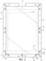
- Fig. 3 is a plan view of the embodiment of Fig. 1 showing the top panel 100 removed and a portable electronic device 128 placed in the protected space between the spacers 104. Not all spacers and slots are numbered to avoid obscuring the drawing.
- the spacers 104 are positioned directly up against the device 128 to prevent any movement of the device within the case.
- the spacers 104 may be moved outward away from the device 128 along the slots 106 and 108 to provide a gap between the device and the spacers.
- the spacers may be moved by loosening the screws 110 and then retightening them after the spacers have been repositioned.
- a second portable electronic device 130 which has a smaller footprint than the first device 128 is shown in phantom outline in Fig. 3 .
- the spacers 104 may be moved inward along the slots 106 and 108 to reposition them against the smaller device 130. If the footprint of any device would result in any of the spacers being positioned directly in the center of one of the X-shaped slots 106, the device may be moved laterally in either or both of the X or Y directions relative to the shells so that the spacers can be away from the centers of any of the X-shaped slots.
- Fig. 4 is a cross-sectional view of an embodiment of a spacer, panels and fasteners according to the inventive principles of this patent disclosure.
- the view of Fig. 4 is taken through a cross-section of the embodiment of Fig. 1 as shown by arrows 4.
- the slots 106 and 108 in the shells 114 and 118 are wide enough to enable the threaded portion of the screws 110 to pass through without interference while still being narrow enough to form a shoulder at surfaces 132 to enable the ends of posts 122 to rest directly against the shells 114 and 118 to provide a rigid connection between the spacers and panels when the screws 110 are tightened into to the posts.
- the slots 124 and 125 in the impact absorbing materials 116 and 120 are wider than the slots 106 and 108 in the shells 114 and 118 to enable the posts 122 to pass through to the shells without interference from the impact absorbing materials.
- the screws may be socket head cap screws.
- the impact absorbing materials 116 and 120 are shown directly abutting the post 122, there can be some space between the impact absorbing materials and the posts, i.e., the slots 124 and 125 can be made wider, without adverse effects.
- the bumper 126 is shown directly abutting the impact absorbing materials 116 and 120, but the bumper may be made shorter, i.e., creating space between the bumper and impact absorbing materials, or longer, i.e., causing deformation of the bumper and/or impact absorbing materials, without adverse effects.
- the shells 114 and 118 may be fabricated from materials that provide a high level of rigidity, strength and/or impact resistance such as reinforced composite panels.
- the shells may be molded from carbon fibers that are woven or otherwise arranged to provide reinforcement and impregnated with epoxy, polyester, vinylester or other suitable resin.
- Alternative fibers such as Kevlar or glass fibers may also be used.
- Other suitable materials for the shells include aluminum, titanium, and various engineering plastics.
- the impact absorbing materials 116 and 120 and/or bumpers 126 may be fabricated from non-linear or non-Newtonian polymers or other foams or elastomeric materials to provide a high level of impact absorption, dissipation, and/or resistance.
- the impact absorbing materials 116 and 120 may be permanently or removably attached to the shells 114 and 118 through any suitable techniques such as adhesives, tapes, hook-and-loop fasteners, etc. Other suitable materials include neoprene or other engineering elastomers.
- the impact absorbing materials may be formed integrally with the shells, for example by creating a hardness gradient in a single material that produces a rigid shell on one side that transitions to a softer cushion on the other.
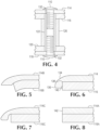
- Figs. 5-8 are cross-sectional views illustrating some possible profiles for the edges of shells and impact absorbing materials according to the inventive principles of this patent disclosure.
- the embodiment of Fig. 6 is the profile used in most of the embodiments of shells illustrated throughout this patent disclosure.
- the profile of the embodiment of Fig. 6 has a maj or radius curvature 134 and minor radius curvature 136 that have been found to provide an appealing touch surface to some consumers, while the sharp inner corner 138 and vertical surface 140 form a convenient well for positioning and/or holding the impact absorbing material 116 in place.
- the shell 114A has a flat outer edge 142 that may provide a more technical feel that appeals to some other consumers.
- the impact absorbing material 116A may be positioned flush with the edge 142 as shown in Fig. 8 , or it may be recessed from the edge in other embodiments.
- the flat edge 142 may also make the shell less expensive to fabricate compared to other profiles.
- Figs. 5 and 7 illustrate other alternative embodiments of edge profiles for shells 114B and 114C, and impact absorbing materials 116B and 116C.
- the embodiments of Figs. 5 and 7 may fall somewhere between the embodiments of Figs. 6 and 8 in terms of cost to manufacture. They may also provide touch surfaces that appeal to yet other groups of consumer.
- One particularly beneficial combination of materials may be the use of carbon-fiber composites for the shells 114 and a microcellular contouring material like Poron XRD from Rogers Corporation for the impact absorbing material 116. This combination may provide a high-end aesthetic feel and appearance due to the high-touch effect and tactile feedback that provides a pleasing sensation to a user.
- the spacers 104 may be fabricated with posts 122 made from aluminum or other metals and bumpers 126 made from neoprene or other elastomer.
- the spacers can be made to have adjustable lengths, for example, by having one portion with an internal thread and another portion with a mating external thread. The length of such a spacer may be adjusted by turning one portion relative to other. A locknut may be added to lock the positions of the two portions once they are adjusted to the desired length.
- the spacers may be fabricated with posts that have external threads at either end and fastened to the shells with nuts.
- the spacers may be fabricated as one-piece components with integral bumpers.
- the spacers may be molded from a single material that is rigid enough to form a strong connection between the shells or panels, but elastic enough to act as an impact absorbing bumper to protect the device.
- the spacers may be fabricated from a single material with a hardness gradient that is rigid on the inside to behave like a post, but more flexible on the outside to behave as a bumper.
- the spacers may be attached to the shells or panels with any other suitable fasteners such as keyed magnets or snaps or other spring-loaded fastening devices. If screws are used, any suitable drive style may be used including security type drives such as spanner, three-wing, one-way, tamper-proof, reverse drive, etc.
- the impact forces may cause the spacer 104A to move in the direction of arrow 148, while the wedging action on the sides of the device 128 may cause spacers 104B and 104C to move in the directions of arrows 150 and 152, respectively.
- the spacers For the spacers to move, they have to overcome the forces of friction holding them in place, thereby diverting impact energy away from the device. This may be in addition to the impact absorbing action of the bumpers on the spacers.
- the rigid material in the shells may also perform multiple functions as they interact with the spacers.
- the rigid shell On the portion of a shell that is inside of the spacers (i.e., over the device), the rigid shell may distribute localized impact forces over a wider area where the forces may be absorbed by more of the impact absorbing material. Outside of the spacers, however, where the rigid shell is unsupported, it may behave as more of an impact absorbing material itself. Therefore, the spacers may form a support boundary where the shell may transition from an impact distributing material to an impact absorbing material.
- the impact forces applied to the outer periphery of a shell may cause the shell material to deform and possibly even fracture. In the case of more rigid and frangible materials like carbon fiber, the shell may eventually fracture, whereas in the case of more flexible materials like Kevlar fiber, the shell may only deform
- the spacers may form various impact absorbing structures with the panels. These structures may absorb impact in various modes of operation, e.g., by causing one or more of the spacers to move relative to at least one of the panels, by causing a material in at least one of the panels to deform temporarily or permanently, and/or causing a rigid material in at least one of the panels to fracture.
- Figs. 9, 9A and 10 illustrate some additional arrangements of attachment slots according to the inventive principles of this patent disclosure.
- the embodiment of Fig. 9 has slots that are perpendicular to the edges of the shells.
- the embodiment of Fig. 9A has a combination of perpendicular and diagonal slots and illustrates an alternative arrangement that may use the same number of spacers (15) as the embodiment of Figs. 1-3 without having intersections in the slots.
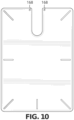
- the embodiment of Fig. 10 illustrates an arrangement in which all of the slots generally radiate outward from the center or centroid of the case, which may correspond approximately with the center of mass of a device in the case.
- the slots may preferably include one or more sections arranged at least partially along a line having a geometric component that runs generally from the center of the case to the periphery of the case.
- the slots need not be linear.
- one or more of the slots may be curved in a manner that causes a non-linear resistance to the motion of a spacer as it slides in the slot in response to impact forces.
- This may be implemented for example with a slot that, at the inner part of the periphery, is arranged along a reference line that runs generally from the center of the case to the periphery of the case, but as the slot extends toward the outer part of the periphery, it curves away from the reference line to create progressively more resistance to movement of the spacer along the slot.
- Fig. 11 illustrates an embodiment of a bumper for a protection system for portable electronic devices according to the inventive principles of this patent disclosure.
- the bumper 154 is shown attached to the embodiment of a case shown in Figs. 1-3 , but the inventive principles are not limited to use with any specific case.
- Fig. 12 is a cross-sectional view of the bumper 154 taken through the section shown by the arrows 12 in Fig. 11 .
- the spacers are sized such that h1 is the distance between the inner surfaces of the impact absorbing materials 116 and 120.
- the bumper 154 includes an outer portion 156 and an inner portion 158 which define an upper groove 160 and a lower groove 162. which engage the outer edges of the shells 114 and 118, respectively. In this configuration, lips 164 and 166 of the outer portion 156 overlap the outer edges of the shells 114 and 118 by a relatively small amount.
- the bumper 154 made from neoprene or other suitable elastomeric material.
- Fig. 13 is another cross-sectional view of the bumper 154 in which shorter spacers are used such that h2 is the relatively smaller distance between the inner surfaces of the impact absorbing materials 116 and 120.
- the outer edges of the shells 114 and 118 sink deeper into the grooves 160 and 162, and the lips 164 and 166 of the outer portion 156 overlap the outer edges of the shells by a larger amount then in Fig. 12 .
- the inner portion 158 of the bumper 154 is shown slightly compressed by shorter distance h2, but depending on the relative hardnesses of the bumper 154 and impact absorbing materials 116 and 120, the impact absorbing materials may be compressed in addition to, or instead of, the bumper 154.
- one or more holes may be included to accommodate a locking devcie for security purposes.
- a TSA lock may be threaded through one or more holes 168 in the panels as shown in Fig. 10 .
- the holes may pass through both of the shells 114 and 118 and both of the protective materials 116 and 120.
- one or more layers of additional materials may be applied over the exposed surfaces of the impact absorbing materials 116 and 120.
- These inner layers may perform various functions.
- the inner layers may protect the layers of impact absorbing materials.
- the inner layers be made of smooth fabric or similar coating to make it easy to slide a device into and out of the protection system.
- the inner layers may be made of a relatively grippy material to prevent the device from falling out of the protective system.
- the inner layers may have a surface that strikes a balance between slipperiness and slip resistance to facilitate purposefully sliding the device into and out of the frame while preventing unintentional removal.
- the impact absorbing materials 116 and 120 maybe selected to have these qualities, thereby eliminating the need for the additional inner layers of materials.
- the system components described above may form an infinitely configurable enclosure offering a protective and lightweight system for keeping laptops, tablet computers and other devices safe and secure.
- the modular construction may allow it to be used for different size devices and grow and/or adapt over time as a user replaces and/or acquires different devices.
- the inventive principles may provide versatile solutions for any or all of the following types of users: individuals who cannot afford to have their laptops and/or tablet computers damaged; individuals who travel with their electronics and have to protect them within checked luggage; individuals who ride motorcycles or bicycles and need to protect their devices against sudden impacts and falls; individuals who upgrade their devices but who don't want to spend money on new cases every time they upgraded their hardware; individuals who value a high-touch and high-end enclosure for their devices; individuals who need two or more cases for multiple devices and can leverage the system's ability to be custom configured for multiple individual devices or multiple devices together protected by a single enclosure; and individuals who want added protection within their laptop bags, backpacks, luggage, and other bags.
Landscapes
- Engineering & Computer Science (AREA)
- Theoretical Computer Science (AREA)
- Computer Hardware Design (AREA)
- Physics & Mathematics (AREA)
- General Engineering & Computer Science (AREA)
- General Physics & Mathematics (AREA)
- Human Computer Interaction (AREA)
- Computer Security & Cryptography (AREA)
- Software Systems (AREA)
- Signal Processing (AREA)
- Casings For Electric Apparatus (AREA)
- Telephone Set Structure (AREA)
- Vibration Dampers (AREA)
Applications Claiming Priority (2)
| Application Number | Priority Date | Filing Date | Title |
|---|---|---|---|
| US201862631415P | 2018-02-15 | 2018-02-15 | |
| PCT/US2019/018259 WO2019161233A1 (en) | 2018-02-15 | 2019-02-15 | Protection systems for portable devices |
Publications (4)
| Publication Number | Publication Date |
|---|---|
| EP3753019A1 EP3753019A1 (en) | 2020-12-23 |
| EP3753019A4 EP3753019A4 (en) | 2021-11-24 |
| EP3753019C0 EP3753019C0 (en) | 2024-04-03 |
| EP3753019B1 true EP3753019B1 (en) | 2024-04-03 |
Family
ID=67620091
Family Applications (1)
| Application Number | Title | Priority Date | Filing Date |
|---|---|---|---|
| EP19754202.0A Active EP3753019B1 (en) | 2018-02-15 | 2019-02-15 | Protection systems for portable devices |
Country Status (6)
| Country | Link |
|---|---|
| US (2) | US11048827B2 (es) |
| EP (1) | EP3753019B1 (es) |
| JP (1) | JP7412005B2 (es) |
| CN (1) | CN112368770B (es) |
| ES (1) | ES2980201T3 (es) |
| WO (1) | WO2019161233A1 (es) |
Families Citing this family (3)
| Publication number | Priority date | Publication date | Assignee | Title |
|---|---|---|---|---|
| US20240275421A1 (en) * | 2021-06-12 | 2024-08-15 | George Tfe Scp | Protective case for mobile device |
| KR102686318B1 (ko) * | 2022-03-31 | 2024-07-22 | (주)세경하이테크 | 굴곡부의 내충격성이 강화된 디스플레이 장치의 백커버 제조방법 |
| CN120743042A (zh) * | 2024-07-10 | 2025-10-03 | 荣耀终端股份有限公司 | 收纳机构和移动终端 |
Family Cites Families (23)
| Publication number | Priority date | Publication date | Assignee | Title |
|---|---|---|---|---|
| KR950030643A (ko) | 1994-04-27 | 1995-11-24 | 김광호 | 화면크기 전환장치 |
| US6567265B1 (en) * | 1995-11-20 | 2003-05-20 | Matsushita Electric Industrial Co., Ltd. | Apparatus having flexible mounting mechanism |
| KR19990008845A (ko) * | 1997-07-04 | 1999-02-05 | 윤종용 | 하드디스크 드라이브의 브이씨엠 댐퍼 |
| JP4353346B2 (ja) * | 2000-06-01 | 2009-10-28 | 富士通株式会社 | 電子機器および電子機器向け内蔵ユニット用緩衝部材 |
| US7609512B2 (en) | 2001-11-19 | 2009-10-27 | Otter Products, Llc | Protective enclosure for electronic device |
| DE602004003739T2 (de) * | 2003-03-31 | 2007-04-05 | Matsushita Electric Industrial Co., Ltd., Kadoma | Stossdämpfendes Element, Stossdämpfendes Verfahren für eine elektronische Vorrichtung welches dieses Element benutzt, und für dieses Element und dieses Verfahren angepasste elektronische Vorrichtung |
| KR100528344B1 (ko) | 2003-08-25 | 2005-11-15 | 삼성전자주식회사 | 내장형 디스크 드라이브의 취부 구조 |
| EP1719042A2 (en) * | 2004-01-07 | 2006-11-08 | Dow Gloval Technologies Inc. | Impact-resistant case with sealable opening |
| US7471509B1 (en) * | 2004-10-08 | 2008-12-30 | Maxtor Corporation | Shock protection for disk drive embedded in an enclosure |
| US8480052B2 (en) * | 2011-01-11 | 2013-07-09 | Drs Tactical Systems, Inc. | Vibration isolating device |
| GB2516540B (en) * | 2011-04-14 | 2015-10-14 | G Form Llc | Protective case and methods of making |
| CN106793622B (zh) * | 2012-04-17 | 2018-11-30 | 青岛科而泰环境控制技术有限公司 | 便携式电器的耐冲击保护壳 |
| JP5806401B2 (ja) * | 2012-05-28 | 2015-11-10 | 京セラ株式会社 | 携帯型電子機器用カバーおよびそれを用いた携帯型電子装置 |
| CN103987214A (zh) * | 2013-02-07 | 2014-08-13 | 英华达(上海)科技有限公司 | 可携式电子装置的机壳及保护外壳 |
| US9871898B2 (en) | 2013-05-08 | 2018-01-16 | Apple Inc. | Ceramic cover for electronic device housing |
| DE102014001726A1 (de) * | 2014-02-07 | 2015-08-13 | Walter Kramer | Schieberventil |
| US20170005686A1 (en) * | 2015-07-01 | 2017-01-05 | iHIDE LLC | Holster system |
| JP5885010B1 (ja) * | 2015-07-02 | 2016-03-15 | パナソニックIpマネジメント株式会社 | カバーおよび携帯電子機器 |
| US9991926B2 (en) * | 2015-09-04 | 2018-06-05 | Asterisk, Inc. | Cover set |
| US10812755B2 (en) * | 2015-10-14 | 2020-10-20 | Utility Associates, Inc. | Article of clothing with video recording device support |
| US10082835B2 (en) * | 2016-02-01 | 2018-09-25 | Hank Technology Llc | Electronic device housings including deformation channels |
| DE102017209254B4 (de) * | 2017-05-31 | 2025-03-06 | Feinmetall Gmbh | Kontaktkopf für eine elektrische Prüfeinrichtung, Prüfeinrichtung |
| JP2019140451A (ja) * | 2018-02-07 | 2019-08-22 | 帝人ファーマ株式会社 | 携帯端末用ケース |
-
2019
- 2019-02-15 WO PCT/US2019/018259 patent/WO2019161233A1/en not_active Ceased
- 2019-02-15 EP EP19754202.0A patent/EP3753019B1/en active Active
- 2019-02-15 ES ES19754202T patent/ES2980201T3/es active Active
- 2019-02-15 JP JP2020543921A patent/JP7412005B2/ja active Active
- 2019-02-15 US US16/278,011 patent/US11048827B2/en active Active
- 2019-02-15 CN CN201980025908.9A patent/CN112368770B/zh active Active
-
2021
- 2021-05-29 US US17/334,711 patent/US12260009B2/en active Active
Also Published As
| Publication number | Publication date |
|---|---|
| ES2980201T3 (es) | 2024-09-30 |
| EP3753019A4 (en) | 2021-11-24 |
| CN112368770B (zh) | 2022-05-24 |
| JP2021514118A (ja) | 2021-06-03 |
| EP3753019A1 (en) | 2020-12-23 |
| EP3753019C0 (en) | 2024-04-03 |
| US20190384940A1 (en) | 2019-12-19 |
| US12260009B2 (en) | 2025-03-25 |
| US20210286907A1 (en) | 2021-09-16 |
| WO2019161233A1 (en) | 2019-08-22 |
| CN112368770A (zh) | 2021-02-12 |
| JP7412005B2 (ja) | 2024-01-12 |
| US11048827B2 (en) | 2021-06-29 |
Similar Documents
| Publication | Publication Date | Title |
|---|---|---|
| US12260009B2 (en) | Protection systems for portable devices | |
| US8004830B2 (en) | Quick-releasing structure for fastening a hard disk, and hard disk carrier and computer system using the same | |
| CN108139771B (zh) | 用于计算装置的保护套及其使用方法 | |
| KR20160049993A (ko) | 강화된 코너 강도를 제공하는 표면 형상을 가진 수화물 케이스 | |
| KR200480739Y1 (ko) | 보호백 | |
| US20140311847A1 (en) | Protective system for luggage | |
| US20140262849A1 (en) | Ergonomic impact damage resistance protector and methods of use thereof | |
| JP2018118050A (ja) | エッジ保護用インサート部材、該インサート部材を含むケース、並びに、その製造及び使用方法 | |
| US8413833B1 (en) | Ruggedized composite rack mount transport case | |
| US20150133202A1 (en) | Portable Electronics Case | |
| EP3554954B1 (en) | Container for housing artwork, kit-of-parts and method | |
| US9352875B1 (en) | Connector element with tang fixation and associated frame assembly with support slats | |
| EP3364801B1 (en) | Helmet having a chin bar collar | |
| TWI771780B (zh) | 補強塊及具有該補強塊的整理箱 | |
| EP1754425A2 (en) | Carrying systems and methods for delicate items | |
| CA2115890A1 (en) | Vibration damping method | |
| US20120172775A1 (en) | Wrist protector | |
| CN109788832B (zh) | 适于电子设备的壳体 | |
| TW201237854A (en) | Hard disc module | |
| KR102274164B1 (ko) | 충격 흡수용 비상 헬멧 | |
| GB2583380A (en) | Suitcase | |
| KR101557695B1 (ko) | 사물함 | |
| US11583972B2 (en) | Vibration absorber for power tools | |
| EP4473868A1 (en) | Torso protector for cyclists | |
| JP4259287B2 (ja) | キャビネット |
Legal Events
| Date | Code | Title | Description |
|---|---|---|---|
| STAA | Information on the status of an ep patent application or granted ep patent |
Free format text: STATUS: THE INTERNATIONAL PUBLICATION HAS BEEN MADE |
|
| PUAI | Public reference made under article 153(3) epc to a published international application that has entered the european phase |
Free format text: ORIGINAL CODE: 0009012 |
|
| STAA | Information on the status of an ep patent application or granted ep patent |
Free format text: STATUS: REQUEST FOR EXAMINATION WAS MADE |
|
| 17P | Request for examination filed |
Effective date: 20200915 |
|
| AK | Designated contracting states |
Kind code of ref document: A1 Designated state(s): AL AT BE BG CH CY CZ DE DK EE ES FI FR GB GR HR HU IE IS IT LI LT LU LV MC MK MT NL NO PL PT RO RS SE SI SK SM TR |
|
| AX | Request for extension of the european patent |
Extension state: BA ME |
|
| DAV | Request for validation of the european patent (deleted) | ||
| DAX | Request for extension of the european patent (deleted) | ||
| A4 | Supplementary search report drawn up and despatched |
Effective date: 20211021 |
|
| RIC1 | Information provided on ipc code assigned before grant |
Ipc: A45C 11/00 20060101ALI20211015BHEP Ipc: G06F 1/16 20060101ALI20211015BHEP Ipc: H04B 1/3888 20150101ALI20211015BHEP Ipc: H04M 1/18 20060101ALI20211015BHEP Ipc: H05K 7/14 20060101ALI20211015BHEP Ipc: H04N 7/01 20060101ALI20211015BHEP Ipc: G11B 33/02 20060101ALI20211015BHEP Ipc: G11B 33/08 20060101AFI20211015BHEP |
|
| GRAP | Despatch of communication of intention to grant a patent |
Free format text: ORIGINAL CODE: EPIDOSNIGR1 |
|
| STAA | Information on the status of an ep patent application or granted ep patent |
Free format text: STATUS: GRANT OF PATENT IS INTENDED |
|
| INTG | Intention to grant announced |
Effective date: 20230915 |
|
| GRAS | Grant fee paid |
Free format text: ORIGINAL CODE: EPIDOSNIGR3 |
|
| RAP3 | Party data changed (applicant data changed or rights of an application transferred) |
Owner name: VALEO CASES LLC |
|
| RIN1 | Information on inventor provided before grant (corrected) |
Inventor name: FERNANDEZ, JUAN |
|
| GRAA | (expected) grant |
Free format text: ORIGINAL CODE: 0009210 |
|
| STAA | Information on the status of an ep patent application or granted ep patent |
Free format text: STATUS: THE PATENT HAS BEEN GRANTED |
|
| AK | Designated contracting states |
Kind code of ref document: B1 Designated state(s): AL AT BE BG CH CY CZ DE DK EE ES FI FR GB GR HR HU IE IS IT LI LT LU LV MC MK MT NL NO PL PT RO RS SE SI SK SM TR |
|
| REG | Reference to a national code |
Ref country code: CH Ref legal event code: EP |
|
| REG | Reference to a national code |
Ref country code: IE Ref legal event code: FG4D |
|
| REG | Reference to a national code |
Ref country code: DE Ref legal event code: R096 Ref document number: 602019049523 Country of ref document: DE |
|
| U01 | Request for unitary effect filed |
Effective date: 20240430 |
|
| U07 | Unitary effect registered |
Designated state(s): AT BE BG DE DK EE FI FR IT LT LU LV MT NL PT SE SI Effective date: 20240529 |
|
| REG | Reference to a national code |
Ref country code: ES Ref legal event code: FG2A Ref document number: 2980201 Country of ref document: ES Kind code of ref document: T3 Effective date: 20240930 |
|
| PG25 | Lapsed in a contracting state [announced via postgrant information from national office to epo] |
Ref country code: IS Free format text: LAPSE BECAUSE OF FAILURE TO SUBMIT A TRANSLATION OF THE DESCRIPTION OR TO PAY THE FEE WITHIN THE PRESCRIBED TIME-LIMIT Effective date: 20240803 |
|
| PG25 | Lapsed in a contracting state [announced via postgrant information from national office to epo] |
Ref country code: HR Free format text: LAPSE BECAUSE OF FAILURE TO SUBMIT A TRANSLATION OF THE DESCRIPTION OR TO PAY THE FEE WITHIN THE PRESCRIBED TIME-LIMIT Effective date: 20240403 |
|
| PG25 | Lapsed in a contracting state [announced via postgrant information from national office to epo] |
Ref country code: GR Free format text: LAPSE BECAUSE OF FAILURE TO SUBMIT A TRANSLATION OF THE DESCRIPTION OR TO PAY THE FEE WITHIN THE PRESCRIBED TIME-LIMIT Effective date: 20240704 |
|
| PG25 | Lapsed in a contracting state [announced via postgrant information from national office to epo] |
Ref country code: CZ Free format text: LAPSE BECAUSE OF FAILURE TO SUBMIT A TRANSLATION OF THE DESCRIPTION OR TO PAY THE FEE WITHIN THE PRESCRIBED TIME-LIMIT Effective date: 20240403 |
|
| PG25 | Lapsed in a contracting state [announced via postgrant information from national office to epo] |
Ref country code: PL Free format text: LAPSE BECAUSE OF FAILURE TO SUBMIT A TRANSLATION OF THE DESCRIPTION OR TO PAY THE FEE WITHIN THE PRESCRIBED TIME-LIMIT Effective date: 20240403 |
|
| PG25 | Lapsed in a contracting state [announced via postgrant information from national office to epo] |
Ref country code: PL Free format text: LAPSE BECAUSE OF FAILURE TO SUBMIT A TRANSLATION OF THE DESCRIPTION OR TO PAY THE FEE WITHIN THE PRESCRIBED TIME-LIMIT Effective date: 20240403 Ref country code: NO Free format text: LAPSE BECAUSE OF FAILURE TO SUBMIT A TRANSLATION OF THE DESCRIPTION OR TO PAY THE FEE WITHIN THE PRESCRIBED TIME-LIMIT Effective date: 20240703 Ref country code: IS Free format text: LAPSE BECAUSE OF FAILURE TO SUBMIT A TRANSLATION OF THE DESCRIPTION OR TO PAY THE FEE WITHIN THE PRESCRIBED TIME-LIMIT Effective date: 20240803 Ref country code: HR Free format text: LAPSE BECAUSE OF FAILURE TO SUBMIT A TRANSLATION OF THE DESCRIPTION OR TO PAY THE FEE WITHIN THE PRESCRIBED TIME-LIMIT Effective date: 20240403 Ref country code: GR Free format text: LAPSE BECAUSE OF FAILURE TO SUBMIT A TRANSLATION OF THE DESCRIPTION OR TO PAY THE FEE WITHIN THE PRESCRIBED TIME-LIMIT Effective date: 20240704 Ref country code: CZ Free format text: LAPSE BECAUSE OF FAILURE TO SUBMIT A TRANSLATION OF THE DESCRIPTION OR TO PAY THE FEE WITHIN THE PRESCRIBED TIME-LIMIT Effective date: 20240403 Ref country code: RS Free format text: LAPSE BECAUSE OF FAILURE TO SUBMIT A TRANSLATION OF THE DESCRIPTION OR TO PAY THE FEE WITHIN THE PRESCRIBED TIME-LIMIT Effective date: 20240703 |
|
| REG | Reference to a national code |
Ref country code: DE Ref legal event code: R097 Ref document number: 602019049523 Country of ref document: DE |
|
| PG25 | Lapsed in a contracting state [announced via postgrant information from national office to epo] |
Ref country code: SK Free format text: LAPSE BECAUSE OF FAILURE TO SUBMIT A TRANSLATION OF THE DESCRIPTION OR TO PAY THE FEE WITHIN THE PRESCRIBED TIME-LIMIT Effective date: 20240403 Ref country code: RO Free format text: LAPSE BECAUSE OF FAILURE TO SUBMIT A TRANSLATION OF THE DESCRIPTION OR TO PAY THE FEE WITHIN THE PRESCRIBED TIME-LIMIT Effective date: 20240403 |
|
| PG25 | Lapsed in a contracting state [announced via postgrant information from national office to epo] |
Ref country code: SM Free format text: LAPSE BECAUSE OF FAILURE TO SUBMIT A TRANSLATION OF THE DESCRIPTION OR TO PAY THE FEE WITHIN THE PRESCRIBED TIME-LIMIT Effective date: 20240403 |
|
| PG25 | Lapsed in a contracting state [announced via postgrant information from national office to epo] |
Ref country code: SM Free format text: LAPSE BECAUSE OF FAILURE TO SUBMIT A TRANSLATION OF THE DESCRIPTION OR TO PAY THE FEE WITHIN THE PRESCRIBED TIME-LIMIT Effective date: 20240403 Ref country code: SK Free format text: LAPSE BECAUSE OF FAILURE TO SUBMIT A TRANSLATION OF THE DESCRIPTION OR TO PAY THE FEE WITHIN THE PRESCRIBED TIME-LIMIT Effective date: 20240403 Ref country code: RO Free format text: LAPSE BECAUSE OF FAILURE TO SUBMIT A TRANSLATION OF THE DESCRIPTION OR TO PAY THE FEE WITHIN THE PRESCRIBED TIME-LIMIT Effective date: 20240403 |
|
| PLBE | No opposition filed within time limit |
Free format text: ORIGINAL CODE: 0009261 |
|
| STAA | Information on the status of an ep patent application or granted ep patent |
Free format text: STATUS: NO OPPOSITION FILED WITHIN TIME LIMIT |
|
| 26N | No opposition filed |
Effective date: 20250106 |
|
| U20 | Renewal fee for the european patent with unitary effect paid |
Year of fee payment: 7 Effective date: 20250226 |
|
| PGFP | Annual fee paid to national office [announced via postgrant information from national office to epo] |
Ref country code: ES Payment date: 20250305 Year of fee payment: 7 |
|
| PGFP | Annual fee paid to national office [announced via postgrant information from national office to epo] |
Ref country code: GB Payment date: 20250225 Year of fee payment: 7 |
|
| PG25 | Lapsed in a contracting state [announced via postgrant information from national office to epo] |
Ref country code: MC Free format text: LAPSE BECAUSE OF FAILURE TO SUBMIT A TRANSLATION OF THE DESCRIPTION OR TO PAY THE FEE WITHIN THE PRESCRIBED TIME-LIMIT Effective date: 20240403 |
|
| REG | Reference to a national code |
Ref country code: CH Ref legal event code: PL |
|
| PG25 | Lapsed in a contracting state [announced via postgrant information from national office to epo] |
Ref country code: CH Free format text: LAPSE BECAUSE OF NON-PAYMENT OF DUE FEES Effective date: 20250228 |
|
| PG25 | Lapsed in a contracting state [announced via postgrant information from national office to epo] |
Ref country code: IE Free format text: LAPSE BECAUSE OF NON-PAYMENT OF DUE FEES Effective date: 20250215 |