EP3751835A1 - Camera module - Google Patents
Camera module Download PDFInfo
- Publication number
- EP3751835A1 EP3751835A1 EP19771656.6A EP19771656A EP3751835A1 EP 3751835 A1 EP3751835 A1 EP 3751835A1 EP 19771656 A EP19771656 A EP 19771656A EP 3751835 A1 EP3751835 A1 EP 3751835A1
- Authority
- EP
- European Patent Office
- Prior art keywords
- electronic component
- flexible board
- rear surface
- terminal
- camera module
- Prior art date
- Legal status (The legal status is an assumption and is not a legal conclusion. Google has not performed a legal analysis and makes no representation as to the accuracy of the status listed.)
- Granted
Links
Images





Classifications
-
- G—PHYSICS
- G03—PHOTOGRAPHY; CINEMATOGRAPHY; ANALOGOUS TECHNIQUES USING WAVES OTHER THAN OPTICAL WAVES; ELECTROGRAPHY; HOLOGRAPHY
- G03B—APPARATUS OR ARRANGEMENTS FOR TAKING PHOTOGRAPHS OR FOR PROJECTING OR VIEWING THEM; APPARATUS OR ARRANGEMENTS EMPLOYING ANALOGOUS TECHNIQUES USING WAVES OTHER THAN OPTICAL WAVES; ACCESSORIES THEREFOR
- G03B17/00—Details of cameras or camera bodies; Accessories therefor
- G03B17/02—Bodies
-
- H—ELECTRICITY
- H04—ELECTRIC COMMUNICATION TECHNIQUE
- H04N—PICTORIAL COMMUNICATION, e.g. TELEVISION
- H04N23/00—Cameras or camera modules comprising electronic image sensors; Control thereof
- H04N23/50—Constructional details
- H04N23/51—Housings
-
- H—ELECTRICITY
- H04—ELECTRIC COMMUNICATION TECHNIQUE
- H04N—PICTORIAL COMMUNICATION, e.g. TELEVISION
- H04N23/00—Cameras or camera modules comprising electronic image sensors; Control thereof
- H04N23/50—Constructional details
- H04N23/54—Mounting of pick-up tubes, electronic image sensors, deviation or focusing coils
-
- H—ELECTRICITY
- H04—ELECTRIC COMMUNICATION TECHNIQUE
- H04N—PICTORIAL COMMUNICATION, e.g. TELEVISION
- H04N23/00—Cameras or camera modules comprising electronic image sensors; Control thereof
- H04N23/50—Constructional details
- H04N23/55—Optical parts specially adapted for electronic image sensors; Mounting thereof
-
- H—ELECTRICITY
- H04—ELECTRIC COMMUNICATION TECHNIQUE
- H04N—PICTORIAL COMMUNICATION, e.g. TELEVISION
- H04N23/00—Cameras or camera modules comprising electronic image sensors; Control thereof
- H04N23/57—Mechanical or electrical details of cameras or camera modules specially adapted for being embedded in other devices
-
- H—ELECTRICITY
- H05—ELECTRIC TECHNIQUES NOT OTHERWISE PROVIDED FOR
- H05K—PRINTED CIRCUITS; CASINGS OR CONSTRUCTIONAL DETAILS OF ELECTRIC APPARATUS; MANUFACTURE OF ASSEMBLAGES OF ELECTRICAL COMPONENTS
- H05K1/00—Printed circuits
- H05K1/02—Details
- H05K1/0277—Bendability or stretchability details
- H05K1/028—Bending or folding regions of flexible printed circuits
-
- H—ELECTRICITY
- H05—ELECTRIC TECHNIQUES NOT OTHERWISE PROVIDED FOR
- H05K—PRINTED CIRCUITS; CASINGS OR CONSTRUCTIONAL DETAILS OF ELECTRIC APPARATUS; MANUFACTURE OF ASSEMBLAGES OF ELECTRICAL COMPONENTS
- H05K1/00—Printed circuits
- H05K1/02—Details
- H05K1/14—Structural association of two or more printed circuits
- H05K1/147—Structural association of two or more printed circuits at least one of the printed circuits being bent or folded, e.g. by using a flexible printed circuit
-
- H—ELECTRICITY
- H05—ELECTRIC TECHNIQUES NOT OTHERWISE PROVIDED FOR
- H05K—PRINTED CIRCUITS; CASINGS OR CONSTRUCTIONAL DETAILS OF ELECTRIC APPARATUS; MANUFACTURE OF ASSEMBLAGES OF ELECTRICAL COMPONENTS
- H05K1/00—Printed circuits
- H05K1/18—Printed circuits structurally associated with non-printed electric components
- H05K1/189—Printed circuits structurally associated with non-printed electric components characterised by the use of flexible or folded printed circuits
-
- H—ELECTRICITY
- H10—SEMICONDUCTOR DEVICES; ELECTRIC SOLID-STATE DEVICES NOT OTHERWISE PROVIDED FOR
- H10F—INORGANIC SEMICONDUCTOR DEVICES SENSITIVE TO INFRARED RADIATION, LIGHT, ELECTROMAGNETIC RADIATION OF SHORTER WAVELENGTH OR CORPUSCULAR RADIATION
- H10F39/00—Integrated devices, or assemblies of multiple devices, comprising at least one element covered by group H10F30/00, e.g. radiation detectors comprising photodiode arrays
- H10F39/80—Constructional details of image sensors
- H10F39/804—Containers or encapsulations
-
- H—ELECTRICITY
- H05—ELECTRIC TECHNIQUES NOT OTHERWISE PROVIDED FOR
- H05K—PRINTED CIRCUITS; CASINGS OR CONSTRUCTIONAL DETAILS OF ELECTRIC APPARATUS; MANUFACTURE OF ASSEMBLAGES OF ELECTRICAL COMPONENTS
- H05K1/00—Printed circuits
- H05K1/02—Details
- H05K1/11—Printed elements for providing electric connections to or between printed circuits
- H05K1/111—Pads for surface mounting, e.g. lay-out
- H05K1/112—Pads for surface mounting, e.g. lay-out directly combined with via connections
- H05K1/113—Via provided in pad; Pad over filled via
-
- H—ELECTRICITY
- H05—ELECTRIC TECHNIQUES NOT OTHERWISE PROVIDED FOR
- H05K—PRINTED CIRCUITS; CASINGS OR CONSTRUCTIONAL DETAILS OF ELECTRIC APPARATUS; MANUFACTURE OF ASSEMBLAGES OF ELECTRICAL COMPONENTS
- H05K1/00—Printed circuits
- H05K1/18—Printed circuits structurally associated with non-printed electric components
- H05K1/181—Printed circuits structurally associated with non-printed electric components associated with surface mounted components
-
- H—ELECTRICITY
- H05—ELECTRIC TECHNIQUES NOT OTHERWISE PROVIDED FOR
- H05K—PRINTED CIRCUITS; CASINGS OR CONSTRUCTIONAL DETAILS OF ELECTRIC APPARATUS; MANUFACTURE OF ASSEMBLAGES OF ELECTRICAL COMPONENTS
- H05K2201/00—Indexing scheme relating to printed circuits covered by H05K1/00
- H05K2201/05—Flexible printed circuits [FPCs]
-
- H—ELECTRICITY
- H05—ELECTRIC TECHNIQUES NOT OTHERWISE PROVIDED FOR
- H05K—PRINTED CIRCUITS; CASINGS OR CONSTRUCTIONAL DETAILS OF ELECTRIC APPARATUS; MANUFACTURE OF ASSEMBLAGES OF ELECTRICAL COMPONENTS
- H05K2201/00—Indexing scheme relating to printed circuits covered by H05K1/00
- H05K2201/05—Flexible printed circuits [FPCs]
- H05K2201/052—Branched
-
- H—ELECTRICITY
- H05—ELECTRIC TECHNIQUES NOT OTHERWISE PROVIDED FOR
- H05K—PRINTED CIRCUITS; CASINGS OR CONSTRUCTIONAL DETAILS OF ELECTRIC APPARATUS; MANUFACTURE OF ASSEMBLAGES OF ELECTRICAL COMPONENTS
- H05K2201/00—Indexing scheme relating to printed circuits covered by H05K1/00
- H05K2201/10—Details of components or other objects attached to or integrated in a printed circuit board
- H05K2201/10007—Types of components
- H05K2201/10121—Optical component, e.g. opto-electronic component
-
- H—ELECTRICITY
- H05—ELECTRIC TECHNIQUES NOT OTHERWISE PROVIDED FOR
- H05K—PRINTED CIRCUITS; CASINGS OR CONSTRUCTIONAL DETAILS OF ELECTRIC APPARATUS; MANUFACTURE OF ASSEMBLAGES OF ELECTRICAL COMPONENTS
- H05K2201/00—Indexing scheme relating to printed circuits covered by H05K1/00
- H05K2201/10—Details of components or other objects attached to or integrated in a printed circuit board
- H05K2201/10007—Types of components
- H05K2201/10151—Sensor
-
- H—ELECTRICITY
- H05—ELECTRIC TECHNIQUES NOT OTHERWISE PROVIDED FOR
- H05K—PRINTED CIRCUITS; CASINGS OR CONSTRUCTIONAL DETAILS OF ELECTRIC APPARATUS; MANUFACTURE OF ASSEMBLAGES OF ELECTRICAL COMPONENTS
- H05K2201/00—Indexing scheme relating to printed circuits covered by H05K1/00
- H05K2201/10—Details of components or other objects attached to or integrated in a printed circuit board
- H05K2201/10227—Other objects, e.g. metallic pieces
- H05K2201/10295—Metallic connector elements partly mounted in a hole of the PCB
- H05K2201/10303—Pin-in-hole mounted pins
-
- H—ELECTRICITY
- H05—ELECTRIC TECHNIQUES NOT OTHERWISE PROVIDED FOR
- H05K—PRINTED CIRCUITS; CASINGS OR CONSTRUCTIONAL DETAILS OF ELECTRIC APPARATUS; MANUFACTURE OF ASSEMBLAGES OF ELECTRICAL COMPONENTS
- H05K3/00—Apparatus or processes for manufacturing printed circuits
- H05K3/0058—Laminating printed circuit boards onto other substrates, e.g. metallic substrates
- H05K3/0064—Laminating printed circuit boards onto other substrates, e.g. metallic substrates onto a polymeric substrate
Definitions
- the applications of the camera module 1 are not limited to vehicle mounting use.
- the dimensions thereof may also be smaller or larger than the dimensions exemplified above.
- the explanation will be given by reference to the example of case where the camera module 1 is one for mounting on a vehicle.
- the number and arrangement of the terminals 7 may be suitably set.
- six terminals 7 are arranged on the center side of the rear surface part 3b (a half of them is shown). Further, the six terminals 7 are arranged in two lines along the side of the rear surface part 3b.
- the image sensor 9 for example has a bare chip, a package sealing the bare chip, and a plurality of leads extending to the outer side and lower side of the package. Further, by bonding the leads to pad-shaped lands on the rigid board 23 by solder or the like, the image sensor 9 is surface-mounted on the rigid board 23.
- the image sensor 9 may be a type mounted by a method other than that described above or may be a bare chip. Further, the image sensor 9 for example may have a color filter and/or lens array etc.
- the rigid board 23 is for example a rigid type printed circuit board.
- the rigid board 23 is for example a double-sided board comprised of a board shaped insulator on the two sides of which conductor layers are formed or a multilayer board comprised of a board shaped insulator on and in which three or more conductor layers are formed. Note that, it is also possible to form the rigid board 23 by single-sided board comprised of a board shaped insulator on only one surface of which a conductor layer is formed.
- the terminal connection part 13a for example faces the inner surface of the rear surface part 3b in the housing 3. Accordingly, from another viewpoint, the flexible board 13 has a rear surface facing part 13c which faces the inner surface of the rear surface part 3b.
- the mutually facing two surfaces need not be parallel.
- the surfaces may be inclined relative to each other or at least one surface may bend.
- the terminal connection part 13a and the rear surface facing part 13c may be grasped as the same ones or may be grasped so that one includes the other.
- the term “terminal connection part 13a” will be used between the two. However, this term may be replaced by the rear surface facing part 13c.
- the control part 37 controls the start of driving and stopping of driving of the driving part 31, first processing part 33, and second processing part 35 in accordance with the control signal input form the terminals 7. Further, for example, the control part 37 supplies a clock pulse to these parts (31, 33, and 35) and performs processing for synchronizing them. Note that, the division of the roles of the driving part 31, first processing part 33, second processing part 35, and control part 37 may be suitably set.
- the power supply part 39 converts the supplied power to power with a suitable voltage and/or current and distributes the results to the parts, therefore a relatively large current flows into the power supply part 39 and a relatively small current flows from the power supply part 39 to the parts. Accordingly, when the power supply part 39 is provided in the assembly 11, a relatively large current flows from the terminals 7 to the assembly 11. On the other hand, when the power supply part 39 is provided on the flexible board 13, a relatively large current flows from the terminals 7 up to the middle of the flexible board 13 and a relatively small current flows from the middle up to the assembly 11. That is, the route through which a relatively large current flows becomes short. As a result, the amount of heat generated by supply of the power is reduced and in turn the amount of heat transferred to the image sensor 9 is reduced.
- each extending part 313d itself and the position of arrangement of the electronic component 15 in each extending part 313d may be made the same as those in the extending part 213d in the second embodiment.
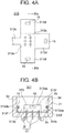
- the widths of the extending parts are different between FIG. 3 and FIG. 4A . However, these widths may be suitably set as explained in the explanation of the second embodiment. Further, it was explained in the explanation of the first embodiment that the division of the roles of the plurality of electronic components 15 for realizing the configuration of the signal processing system in FIG. 2 may be suitably set. The same is true for the plurality of electronic components 15 mounted in the plurality of extending parts 313d.
Landscapes
- Engineering & Computer Science (AREA)
- Multimedia (AREA)
- Signal Processing (AREA)
- Microelectronics & Electronic Packaging (AREA)
- Physics & Mathematics (AREA)
- General Physics & Mathematics (AREA)
- Studio Devices (AREA)
- Camera Bodies And Camera Details Or Accessories (AREA)
- Structure Of Printed Boards (AREA)
- Combinations Of Printed Boards (AREA)
Abstract
Description
- The present disclosure relates to a camera module.
- There is known a camera module utilized as an element of a system such as a vehicle-mounted camera module (for example Patent Literature 1). The camera module in
Patent Literature 1 has a housing, a lens exposed at the front surface of the housing, and a terminal for external connection use which is exposed at a rear surface of the housing. At the inside part of the housing, in order from the lens side to the terminal side, an image sensor, a rigid type first circuit board on which the image sensor is mounted, a rigid type second circuit board connected to the first circuit board, and a flexible board connecting the second circuit board and the terminal are provided. On the second circuit board, a circuit chip (electronic component) is mounted. The flexible board has a signal line pattern part connecting the second board and the terminal and a GND line pattern part which is branched from the signal line pattern part. The GND pattern part is connected to a shield case in the housing. - Patent Literature 1: Japanese Patent Publication No.
2011-166012 - A camera module according to one aspect of the present disclosure includes a housing, a lens, an assembly, a terminal, a flexible board, and an electronic component. The housing includes a front surface part, a rear surface part on the opposite side to that, and a side surface part connecting the front surface part and the rear surface part. The lens is exposed from the front surface part. The assembly includes an image sensor and is located on the rear surface part side relative to the lens . The terminal is located at the rear surface part for connection with an outside part. The flexible board includes a part extending from the assembly toward the terminal. The electronic component is mounted on the flexible board.
- A camera module according to one aspect of the present disclosure includes a housing, a lens, an assembly, a terminal, a connection member, and an electronic component. The housing includes a front surface part, a rear surface part on the side opposite to that, and a side surface part connecting the front surface part and the rear surface part. The lens is exposed from the front surface part. The assembly includes an image sensor and is located on the rear surface part side relative to the lens. The terminal is located at the rear surface part for connection with an outside part. The connection member is a flexible one extending from the assembly toward the terminal. The electronic component is electrically connected to the assembly and the terminal and is located separated from the assembly toward the rear surface part side in the housing.
-
-
FIG. 1 is a schematic perspective view showing cutaway a camera module according to a first embodiment. -
FIG. 2 is a block diagram showing the configuration of a signal processing system in a camera module inFIG. 1 . -
FIG. 3 is a schematic perspective view showing cutaway a camera module according to a second embodiment. -
FIG. 4 is a schematic perspective view cutaway showing a camera module according to a third embodiment. -
FIG. 5 is a schematic perspective view showing cutaway a camera module according to a fourth embodiment. -
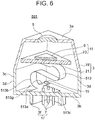
FIG. 6 is a schematic perspective view showing cutaway a camera module according to a fifth embodiment. -
FIG. 7 is a schematic perspective view showing cutaway a camera module according to a sixth embodiment. -
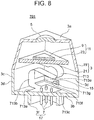
FIG. 8 is a schematic perspective view showing cutaway a camera module according to a seventh embodiment. -
FIG. 9A, FIG. 9B, and FIG. 9C are a cross-sectional view, a top view, and a bottom view showing an example of a flexible board having a reference potential layer. - Below, embodiments of the present disclosure will be explained with reference to the drawings. Note that, the drawings used in the following explanation are schematic ones. Accordingly, for example, sometimes details will be omitted. Further, size ratios etc. in the drawings do not always coincide with the actual ones.
- In the second and following embodiments, configurations common with or resembling already explained configurations use notations attached to the already explained configurations or sometimes illustration and explanation will be omitted. Note that, the configurations corresponding to (resembling) the already explained configurations may be made the same as the already explained configurations for points which are not particularly explained even in a case where notations different from those for the already explained configurations are attached.
-
FIG. 1 is a schematic perspective view showing cutaway acamera module 1 according to afirst embodiment 1. - The
camera module 1 is for example one for mounting on a vehicle and is utilized for drive assistance and/or drive recording and the like. For example, thecamera module 1 is made a size with vertical, horizontal, and height dimensions of 1 cm to 5 cm and is provided inside or outside the car body in an orientation capturing images at the front, rear, or lateral sides of the car body. Thecamera module 1 is electrically connected to a not shown ECU (electronic control unit or engine control unit) and is controlled by the ECU. Further, the signal output from thecamera module 1 is processed by the ECU. - Note that, the applications of the
camera module 1 are not limited to vehicle mounting use. The dimensions thereof may also be smaller or larger than the dimensions exemplified above. However, below, sometimes the explanation will be given by reference to the example of case where thecamera module 1 is one for mounting on a vehicle. - The
camera module 1 for example has ahousing 3, alens 5 exposed from thehousing 3, and a plurality ofterminals 7 for external connection use positioned on the side opposite to thelens 5 in thehousing 3. As will be understood from the position of thelens 5, in thecamera module 1, the upper part side on the drawing sheet is made the imaging side. Further, the vertical direction on the drawing sheet is a direction of an optical axis. The plurality ofterminals 7 are connected through a not shown cable to the ECU when thecamera module 1 is one for mounting in a vehicle. - Further, the
camera module 1, in the inside part of thehousing 3, has anassembly 11 including animage sensor 9, aflexible board 13 which extends from theassembly 11 toward the plurality ofterminals 7, and anelectronic component 15 mounted on theflexible board 13. By these, for example, an image formed on theimage sensor 9 by thelens 5 is converted to an electrical signal which is output from any of the plurality ofterminals 7. Although not particularly shown, thecamera module 1 may have for example a shield case other than the parts described above. - The signal output from the
camera module 1 is for example a signal including information (image data) for reproducing the captured image. Thecamera module 1, for example, outputs a plurality of image data (a plurality of frames of image data) obtained along with the elapse of time in order and thereby contribute to provision of the information of a moving picture image. Note that, thecamera module 1 may be one used for the purpose of acquiring a still image according to need. Further, thecamera module 1 may output information of some sort of result of judgment based on the image data in addition to or in place of the signal of the image data. - The
housing 3 includes for example a part holding the lens 5 (front surface part 3a, lens barrel), a part accommodating theassembly 11 etc., and a part configuring a connector 17 (connector housing part 3f). Note that, in this way, in the explanation of the present embodiment, the term "housing" designates not only a pure box-shaped part, but also a relatively wide part. The inside part of thehousing 3 is for example basically sealed. - The outer shape of the
housing 3 may be made a suitable one. In the example shown, the outer shape of thehousing 3 is substantially the shape of a combination of a right prism having a square bottom surface (terminal 7 side) and a frustum having a square bottom surface (lens 5 side). From another viewpoint, thehousing 3, when viewed in the direction of the optical axis, has a substantially rectangular outer shape.FIG. 1 becomes a schematic perspective view cut along one diagonal line of that rectangle. Further, theconnector housing part 3f is formed in a cylindrical shape projecting so as to surround the plurality ofterminals 7. The "cylinder" referred to here may be circular or rectangular when viewed in the connection direction (here, the same direction as the direction of the optical axis). - Naturally, the outer shape of the
housing 3 is not limited to the above shape. For example, the schematic shape of the outer shape of thehousing 3 may rectangular cuboid shape, may be a shape of a combination of a rectangular cuboid shape (terminal 7 side) and a right circular cylinder (lens 5 side) projecting from the rectangular cuboid shape, may be a right prism having a polygonal shape other than a square (for example a pentagon) as the bottom surface, may be a combination of such a right prism (terminal 7 side) and a right circular cylinder (lens 5 side) projecting from the right prism, may be a right circular cylinder, or may be a shape having a higher design sense. Each right circular cylinder mentioned above may be a part formed as a lens barrel holding thelens 5. Note that, below, as in the example shown, sometimes the explanation will be given with reference to the example of a case where the outer shape of thehousing 3 includes a part of a rectangular cuboid shape or a right prism shape on theterminal 7 side. - The shape of the internal spade of the housing 3 (shape of the inner surface) may also be a suitable shape. In the example shown, the shape of the internal space of the
housing 3 becomes substantially a similar shape to the outer shape of thehousing 3 explained above. Accordingly, thehousing 3 has substantially a rectangular cuboid space on at least the terminal 7 side. From another viewpoint, thehousing 3, on theterminal 7 side, has a flat inner surface (inner surface of therear surface part 3b) perpendicular to the optical axis and a flat wall surface (inner surface of theside surface part 3d) surrounding the four sides of the former surface. - Naturally, the shape of the internal space of the
housing 3 is not limited to the above shape. For example, it may be a shape that includes a polygonal prism other than a quadratic prism or may be a right circular cylinder on theterminal 7 side as well. However, in the following explanation, sometimes the explanation will be given with reference to the example of a case where a substantially rectangular cuboid-shaped space is formed on theterminal 7 side. - When considered dividing the
housing 3 into a plurality of portions, for example, thehousing 3 has afront surface part 3a facing an image capturing side (front side of the lens 5), arear surface part 3b on the opposite side to that, and an outercircumferential surface part 3c (side surface part 3d) joining thefront surface part 3a and therear surface part 3b. The outercircumferential surface part 3c is a part which joins thefront surface part 3a and therear surface part 3b over their entire circumferences. In the outercircumferential surface part 3c, the parts forming the sides of a polygon when viewed in the direction of the optical axis will be referred to as "side surface parts 3d" . In the example shown, the outercircumferential surface part 3c has fourside surface parts 3d since the outer shape of thehousing 3 includes the right prism-shaped part on at least the terminal 7 side. - As will be understood from the above explanation of the outer shape of the
housing 3, the shapes of the outer surfaces of these parts (3a to 3d) may be made suitable shapes. In the example shown, the outer surface of thefront surface part 3a configures the upper bottom of a frustum. The outer surface of therear surface part 3b configures the bottom surface of a right prism (terminal 7 side). The outer surface of the outercircumferential surface part 3c (side surface part 3d) configures the side surface of the frustum and side surfaces of the right prism. - Note that, boundaries of the parts (3a to 3d) may be suitably defined in accordance with the outer shape of the
housing 3. For example, unlike the example shown, when the outer shape of thehousing 3 is a shape of a combination of a rectangular cuboid (terminal 7 side) and a right circular cylinder (lens 5 side) projecting from the rectangular cuboid, thefront surface part 3a may be defined as the part configuring the bottom surface on thelens 5 side in the right circular cylinder or may be defined as the part configuring the entire right circular cylinder and the plane on the right circular cylinder side in the rectangular cuboid. - The shapes of the parts (3a to 3d) may be suitably set so that the shapes of the outer surface and inner surface of the
housing 3 explained above are realized. In the example shown, each of thefront surface part 3a,rear surface part 3b, and outercircumferential surface part 3c is substantially formed in a plate shape with a substantially constant thickness which has the direction in which its outer surface faces as the thickness direction. Note that, the plate shape referred to here includes not only a flat plate shape (example shown), but also a curved plate shape (for example a plate shape that configures a circular cylinder). - Naturally, the shape of each part (3a to 3d) is not limited to a plate shape having the direction in which its outer surface faces as the thickness direction as described above. For example, the
housing 3 may include a cylindrical part around the optical axis (lens barrel holding the lens 5) and thefront surface part 3a may be the front end part of that cylindrical part (edge part of the cylinder). - The
housing 3 is for example formed by a plurality of members in combination. The divided positions of the housing 3 (positions of boundaries among the plurality of members) and the number of the plurality of members etc. may be suitably set. For example, thehousing 3 has afront side housing 19 on thelens 5 side and arear side housing 21 on the opposite side to that. - The
front side housing 19 is a member with a box shape opened on the side opposite to the lens 5 (the box is not limited to a rectangular cuboid shape, same is true for the following explanation). Therear side housing 21 is the box-shaped member opened on thelens 5 side. Further, the opening sides of the two are connected to each other to thereby configure thehousing 3. The two may be connected according to known various methods such as engagement, screwing, bonding, or the like. Further, one opening side edge part may be fit at the inner side of the other opening side edge part as well. - Although not particularly shown, each of the
front side housing 19 and therear side housing 21 may be configured by further more members. For example, thefront side housing 19 may be configured by a lens barrel holding thelens 5 and a member configuring at least thelens 5 side part in the outercircumferential surface part 3c fixed to each other. They may be fixed indirectly through another member in thehousing 3 as well. Further, for example, therear side housing 21 may be configured by a member configuring a part other than aconnector housing part 3f in therear side housing 21 and a member configuring theconnector housing part 3f fixed to each other as well. - The material of the
housing 3 is for example basically made an insulating material. The insulating material is for example a resin. Note that, use may be made of a ceramic or other insulating material as well. Further, in thehousing 3, a conductor (metal) may be used in part or the entirety as well. For example, thehousing 3 may be one formed by burying a metal (shield case) in a resin or may be one which is basically made of a resin and has a conductive paint coated at a suitable position on the inner surface. - The
lens 5 may be a single lens made of a uni-lens or may be a lens group (optical system) formed by a plurality of lenses. Thelens 5 is arranged in the opening formed in thefront surface part 3a and is exposed to the outside part of thehousing 3. Further, thelens 5 focuses the light from the outside part of thehousing 3 and forms an image in the inside part of the housing 3 (on the image sensor 9). Note that, when referring to the fact that thelens 5 is exposed from thefront surface part 3a, this means that thelens 5 can be seen from thefront surface part 3a side and need not always contact the outside air. Accordingly, for example, thelens 5 may be covered by a transparent cover configuring a part of thehousing 3 as well. Note that, it is also possible to grasp the transparent cover as a part of thelens 5. - The
terminal 7 is for example configured by a pin-shaped metal. Eachterminal 7 is for example inserted into a hole formed in therear surface part 3b and is fixed with respect to therear surface part 3b by solder or another bonding material. Further, the plurality ofterminals 7 are for example inserted into holes formed in aflexible board 13 and are bonded with respect to the wirings (conductive pattern) of theflexible board 13 by solder or another conductive bonding material. - Note that, the bonding material bonding the
terminals 7 to therear surface part 3b and the bonding material bonding theterminals 7 to theflexible board 13 may be materials which are different from each other or may be materials which are the same as each other. In the latter case, the two may be separately supplied and cured or may be simultaneously supplied and cured. - The number and arrangement of the
terminals 7 may be suitably set. In the example shown, sixterminals 7 are arranged on the center side of therear surface part 3b (a half of them is shown). Further, the sixterminals 7 are arranged in two lines along the side of therear surface part 3b. - The plurality of
terminals 7 andconnector housing part 3f configure theconnector 17. Thisconnector 17 is for example connected with the not shown other side connector which fits in theconnector housing part 3f. The other side connector has hole parts in which the pin-shapedterminals 7 fit. The inner surfaces of the hole parts are provided with terminals abutting against theterminals 7. - Note that, the male type and the female type may be inverse to the above as well. That is, the
terminals 7 may be ones which are formed on the inner surfaces of the holes into which the pins are inserted as well. In this case, theterminals 7 may be for example metal members having suitable shapes abutting against the outer circumferential surfaces of the pins . The shape of the metal members may be for example flat plate shapes, may be cylindrical shapes into which the pins are inserted, or may be shapes including plate spring parts. - The
assembly 11 for example has the already mentionedimage sensor 9 and arigid board 23 on which theimage sensor 9 is mounted. - The
image sensor 9 is for example configured by a CMOS (complementary metal oxide semiconductor) or CCD (charge coupled device) or another solid state image sensor. Although not particularly shown, theimage sensor 9 has a plurality of pixels which are vertically and horizontally arranged on a light receiving surface on thelens 5 side. Each pixel is configured including a photoelectric conversion element, converts light incident upon each pixel to an electrical signal having a signal strength in accordance with the amount of the light, and outputs the result. Due to this, image data (raw data) of an image formed on the light receiving surface of theimage sensor 9 by thelens 5 is generated. - Further, although not particularly shown, the
image sensor 9 for example has a bare chip, a package sealing the bare chip, and a plurality of leads extending to the outer side and lower side of the package. Further, by bonding the leads to pad-shaped lands on therigid board 23 by solder or the like, theimage sensor 9 is surface-mounted on therigid board 23. Note that, theimage sensor 9 may be a type mounted by a method other than that described above or may be a bare chip. Further, theimage sensor 9 for example may have a color filter and/or lens array etc. - The
rigid board 23 contributes to for example fixation (positioning) of theimage sensor 9 with respect to the housing 3 (lens 5), mounting of not shown electronic components, and the like. Theimage sensor 9 is for example electrically connected through therigid board 23 with the other electronic components and/orflexible board 13 which are connected to therigid board 23. - The
rigid board 23 is for example a rigid type printed circuit board. Therigid board 23 is for example a double-sided board comprised of a board shaped insulator on the two sides of which conductor layers are formed or a multilayer board comprised of a board shaped insulator on and in which three or more conductor layers are formed. Note that, it is also possible to form therigid board 23 by single-sided board comprised of a board shaped insulator on only one surface of which a conductor layer is formed. - The planar shape of the
rigid board 23, the material of the insulator, the material of the conductor layers, and the conductor patterns included in the conductor layers etc. may be suitable ones. For example, the insulator may be one formed by a glass fabric or other base material in which a resin is impregnated or may be a ceramic. The conductor layer may form lands for mounting the electronic components and wirings connecting the lands to each other plus inductors or capacitors or other parts. Therigid board 23 may have an insulation film (solder resist) covering the conductor layer for reducing unwanted short-circuiting of the conductor layer. - The rigid board 23 (image sensor 9) is arranged facing the
lens 5. Therigid board 23 is for example arranged so that the light receiving surface of theimage sensor 9 is substantially positioned at a rear side focal point of thelens 5. When therigid board 23 is arranged with respect to thehousing 3 in this way, the size of the space on the side closer to theterminals 7 than therigid board 23 in thehousing 3 may be suitably set. For example, the distance from therigid board 23 to the inner surface of therear surface part 3b (height of the space on theterminal 7 side) may be made longer than the distance from thelens 5 to theimage sensor 9. - The
rigid board 23 may be suitably fixed with respect to thehousing 3. For example, although not particularly shown, thehousing 3 has a plurality of rods which extend from thefront surface part 3a toward theterminal 7 side. On the other hand, therigid board 23 has a plurality of holes into which the rods are inserted. Further, after theimage sensor 9 and other electronic component are mounted, therigid board 23 is fixed with respect to thehousing 3 by insertion of the rods into the plurality of holes and bonding to the rods by solder or another bonding material. Other than this, for example, the surface on thelens 5 side in therigid board 23 may be bonded to the end surface on theterminal 7 side in a member including a lens barrel holding thelens 5 as well. - As will be understood from the above description, the
rigid board 23 may be fixed with respect to the member holding thelens 5 in thehousing 3 in a manner by which it is impossible to change the position relationships between thelens 5 and theimage sensor 9 without breaking the bonding material etc. Note that, at the time of fixing the board, the image captured by theimage sensor 9 through thelens 5 may be confirmed while positioning thelens 5 and theimage sensor 9. - Various electronic components other than the
image sensor 9 may be mounted on therigid board 23. For example, ICs (integrated circuits), diodes, transistors, resistors, inductors, and/or capacitors may be mounted on therigid board 23. The electronic components may be active elements or may be passive elements. The IC may be an ISP (image signal processor) processing raw data from theimage sensor 9 as well. - Further, although not particularly shown, a connector for connecting the
flexible board 13 to therigid board 23 may be mounted on therigid board 23 as well. The connector is for example mounted on the surface on theterminal 7 side of therigid board 23. The configuration of the connector may be suitable one. For example, the connector may be one configuring a combination of male type and female type connectors together with a connector mounted on theflexible board 13. Further, for example, the connector may be one having a plurality of terminals on the inner wall surface of a slit and with part of theflexible board 13 inserted in the slit. Note that, therigid board 23 and theflexible board 13 can be connected by solder or the like without using a connector. Further, they can be connected on thelens 5 side in therigid board 23. - The
flexible board 13 contributes to connection of the rigid board 23 (image sensor 9) and the plurality ofterminals 7. Further, theflexible board 13 provides a region for mounting theelectronic component 15 and in turn contributes to connection of theelectronic component 15 and the other parts (23, 9, and/or 7 etc.) - The
flexible board 13 is for example a printed circuit board having flexibility (that is, FPC: flexible printed circuit) . Theflexible board 13 may be one comprised of an insulating film on the two surfaces on which having conductor layers, may be one comprised of an insulating layer on only one surface of which having a conductor layer, or may be one comprised of the formers stacked together and having three or more conductor layers. Theflexible board 13 may have an insulation film (solder resist) covering the conductor layer for reducing unwanted short-circuiting of the conductor layer. The inductors or capacitors or other parts may be configured by the conductor layer of theflexible board 13 as well. Theflexible board 13 may be one having flexibility equally over its entirety or may be one having flexibility made relatively higher in the part where bending is planned. - The
flexible board 13 for example has aterminal connection part 13a connected to the plurality ofterminals 7 and arelay part 13b extending from theterminal connection part 13a up to theassembly 11. - The
terminal connection part 13a for example faces the inner surface of therear surface part 3b in thehousing 3. Accordingly, from another viewpoint, theflexible board 13 has a rearsurface facing part 13c which faces the inner surface of therear surface part 3b. Note that, when referring to "face", the mutually facing two surfaces need not be parallel. For example, the surfaces may be inclined relative to each other or at least one surface may bend. Further, in the present embodiment, theterminal connection part 13a and the rearsurface facing part 13c may be grasped as the same ones or may be grasped so that one includes the other. In the explanation in the present embodiment, between the two, mainly the term "terminal connection part 13a" will be used. However, this term may be replaced by the rearsurface facing part 13c. - The
terminal connection part 13a has a size large enough to extend over the range where the plurality ofterminals 7 are arranged. The plurality ofterminals 7 are inserted into theterminal connection part 13a as already explained. Theterminal connection part 13a may be suitably set in the planar shape, the size for the range where the plurality ofterminals 7 are arranged, and the size relative to the inner surface of therear surface part 3b. In the example shown, theterminal connection part 13a is given substantially a rectangular shape smaller than the inner surface of therear surface part 3b. From another viewpoint, theterminal connection part 13a is shaped so as to have outer edges extending along the outer edges of therear surface part 3b (for example substantially similar shape) . Note that, theterminal connection part 13a may have a size equal to the inner surface of therear surface part 3b as well. - The
terminal connection part 13a may be bonded by an adhesive or the like (bonding layer) to the inner surface of therear surface part 3b or need not be so bonded. However, when theterminals 7 are bonded with respect to theterminal connection part 13a andrear surface part 3b as in the above explanation, theterminal connection part 13a is at least fixed with respect to therear surface part 3b directly or indirectly through theterminals 7 at the positions of theterminals 7. - The
terminal connection part 13a may be superposed on the inner surface of therear surface part 3b directly or indirectly through a suitable material (may be directly or indirectly in close contact with the inner surface) or may be separated from the inner surface of therear surface part 3b through a clearance. As the material interposed between theterminal connection part 13a and therear surface part 3b as described above, for example, an adhesive or grease can be mentioned. - When the
terminal connection part 13a is directly or indirectly in close contact with the inner surface of therear surface part 3b, compared with a case where there is a clearance (air) between the two, the heat dissipation property from theterminal connection part 13a to thehousing 3 is improved. The region where theterminal connection part 13a is in close contact with the inner surface of therear surface part 3b is for example 80% or more or the entirety of the area of theterminal connection part 13a. As will be explained later, theelectronic component 15 is mounted on theterminal connection part 13a. The close contact region includes for example a region where theelectronic component 15 is mounted. - Note that, when at least a part of the
terminal connection part 13a is directly or indirectly in close contact with the inner surface of therear surface part 3b without an adhesive interposed, spacing of theterminal connection part 13a from therear surface part 13b may be suitably suppressed. For example, bonding of theterminals 7 and theterminal connection part 13a may contribute to the above adhesion. Further, for example, a not shown member pushing theterminal connection part 13a against therear surface part 3b may be provided as well. Further, for example, therelay part 13b is folded as will be explained later. Therefore, when therelay part 13b generates a restoring force returning it to the flat state, this restoring force may be utilized as well. - The
relay part 13b extends out of a part of the outer edge of theterminal connection part 13a. The connection position of therelay part 13b with respect to theterminal connection part 13a and the shape, size, etc. of therelay part 13b may be suitably set. In the example shown, therelay part 13b extends out of the center side part of one side of the rectangularterminal connection part 13a with a width shorter than the length of the one side. Note that, therelay part 13b may have an equal width to the length of the one side as well. - Further, in the example shown, when the
flexible board 13 is laid out to a flat state, therelay part 13b is substantially formed in a long shape so as to linearly extend with a constant width. Further, therelay part 13b is accommodated in thehousing 3 in a state where it is folded back and forth a suitable number of times. In the example shown, therelay part 13b is folded two times (substantially formed in an S-shape). - Note that, the number of times of folds of the
relay part 13b may be one or may be three or more. Further, the space in which therelay part 13b is accommodated is more specifically the space between the assembly 11 (rigid board 23) and therear surface part 3b (terminal connection part 13a) . This space is secured relatively large as explained in the explanation of the position where therigid board 23 is arranged. - The end part of the
relay part 13b on therigid board 23 side is connected to therigid board 23 as already explained. There may be various methods of connection as already explained. Note that, in the example shown, therelay part 13b is made broader in width in the end part on therigid board 23 side. Due to this, for example, the majority (for example 60% or more of the length) of therelay part 13b is made relatively thin, while an area required for mounting the connector etc. can be secured on therigid board 23 side. Naturally, therelay part 13b may be constant in the width over its entirety as well. - The
electronic component 15 is for example an IC, diode, transistor, resistor, inductor, or capacitor. As will be understood from the above illustration, theelectronic component 15 may be an active element or may be a passive element. - The
electronic component 15 is for example mounted on theterminal connection part 13a of theflexible board 13. More specifically, in theterminal connection part 13a, theelectronic component 15 is mounted in the region outside the range where the plurality ofterminals 7 are arranged. Further, between the two surfaces of theterminal connection part 13a, theelectronic component 15 is mounted on the surface on the side opposite to therear surface part 3b. With respect to the plurality ofterminals 7, theelectronic component 15 may be positioned on therelay part 13b side, may be positioned on the side opposite to therelay part 13b, or may be positioned on a lateral side of a direction toward therelay part 13b (example shown). - Note that, it is also possible to view the
flexible board 13 as having aterminal connection part 13a, arelay part 13b extending out of part of the edge part of theterminal connection part 13a, and an extendingpart 13d which extends out of another part of the edge part of theterminal connection part 13a and theelectronic component 15 as being mounted on the extendingpart 13d. However, in the present embodiment, basically the explanation will be given while viewing theelectronic component 15 as being mounted on theterminal connection part 13a. As will be understood from the shape of the extendingpart 13d, when referring to part of theflexible board 13 extending out (or extends), the part need not have a shape longer in the extending direction. The width may be larger than the length in the extending direction as well. - In the example shown, one
electronic component 15 is mounted. However, the number ofelectronic component 15 is not limited to one. Two or moreelectronic components 15 may be mounted on theterminal connection part 13a as well. Also in the embodiments which will be explained later, basically, the minimum number ofelectronic parts 15 required for the explanation will be shown. However, a greater number (or smaller number) ofelectronic components 15 than the number shown may be provided. - The
electronic component 15 is for example a surface-mounted type. Although not shown here, it is mounted to theflexible board 13 by bonding a plurality of pads or a plurality of leads with respect to pad-shaped lands provided on one major surface of theflexible board 13 by solder or another bonding material. Note that, it is also possible to form theelectronic component 15 as an insert and mount type by inserting a lead into theflexible board 13. - When the
relay part 13b of theflexible board 13 is bent in an S-shape as in the example shown, the surface of therelay part 13b facing therigid board 23 and the surface of theterminal connection part 13a in theflexible board 13 which faces the inside part side of the housing 3 (surface on the side opposite to therear surface part 3b) become the same surface of theflexible board 13. Accordingly, when theflexible board 13 is connected to therigid board 23 by a not shown connector which is surface-mounted on theflexible board 13, the connector and theelectronic component 15 may be mounted on the same major surface of theflexible board 13 and in turn theflexible board 13 may be made a single-sided substrate. -
FIG. 2 is a block diagram showing the configuration of a signal processing system in thecamera module 1. - The
camera module 1 has thelens 5 andimage sensor 9 as already explained. Further, thecamera module 1 has for example a drivingpart 31 driving theimage sensor 9, afirst processing part 33 processing the signal output by theimage sensor 9, asecond processing part 35 processing the signal output by thefirst processing part 33, acontrol part 37 integrally controlling them, and apower supply part 39 supplying power to the parts (31, 33, 35, and 37). - The driving
part 31 for example generates a pulse signal for initialization and a pulse signal (driving signal) having a predetermined frequency for signal transfer in theimage sensor 9 and inputs the results to theimage sensor 9. Receiving the driving signal, theimage sensor 9 outputs a signal in accordance with the captured image (signal of image data). The drivingpart 31 for example outputs a pulse signal to theimage sensor 9 so that the signal of the image data is continuously (repeatedly) output. Due to this, data of a moving picture image is obtained from theimage sensor 9. - The
first processing part 33 andsecond processing part 35, for example, as a whole, perform the predetermined processing on the signal from theimage sensor 9 and outputs the processed signal to theterminals 7. The processing carried out by these processing parts on the signal from theimage sensor 9 is for example amplification, A/D conversion, filtering, AE (automatic exposure), AWB (auto white balance), serial conversion, adding a header or other suitable information, and/or D/A conversion. Note that, the header includes for example information specifying the order of images in a plurality of frames. - The
first processing part 33 andsecond processing part 35 perform the processing as described above suitably divided. For example, thefirst processing part 33 performs processing on the signal of raw data from theimage sensor 9. On the other hand, thesecond processing part 35 performs processing on the signal after processing by thefirst processing part 33 and outputs the processed signal to theterminals 7. Up to which processing thefirst processing part 33 performs can be suitably set. Note that, thefirst processing part 33 and thesecond processing part 35 can also perform the same processing divided between them. - The form of the signal which is output from the
second processing part 35 to theterminals 7 may be made a suitable one. For example, the signal may be an LVDS (low voltage differential signaling) signal. In this case, thesecond processing part 35 for example may be configured including an electronic component converting a signal including information to be output to an LVDS signal as well. Note that, the signal which is output from thesecond processing part 35 to theterminals 7 is not limited to LVDS. For example, it may be a single end signal as well. - The
control part 37, for example, controls the start of driving and stopping of driving of the drivingpart 31,first processing part 33, andsecond processing part 35 in accordance with the control signal input form theterminals 7. Further, for example, thecontrol part 37 supplies a clock pulse to these parts (31, 33, and 35) and performs processing for synchronizing them. Note that, the division of the roles of the drivingpart 31,first processing part 33,second processing part 35, and controlpart 37 may be suitably set. - Note that, the types of the input signals to the parts (9, 31, 33, 35, and 37) and the output signals from the parts, the levels of the signal strength (for example voltages), and/or frequencies etc. may be suitably set. For example, the frequency of the signal which is output from the
second processing part 35 to theterminal 7 as explained above is 500 MHz to 10 GHz or 1G Hz to 10 GHz. - The
power supply part 39 converts an electrical power supplied from theterminals 7 to an electrical power having a suitable voltage, current, and/or frequency (in a case of AC current) and supplies the power to the parts (31, 33, 35, and 37) . The voltage, current, and/or frequency of the power supplied from theterminals 7 to thepower supply part 39 may be suitable one. For example, the current supplied to thepower supply part 39 is 100 mA to 1A or 400 mA to 1A. - The hardware configurations of the driving
part 31,first processing part 33,second processing part 35,control part 37, andpower supply part 39 shown inFIG. 2 may be suitable ones. For example, these functional parts (31, 33, 35, 37, and 39) are configured by one or more ICs. Among these functional parts, two or more functional parts may be configured by one IC. Conversely, one functional part may be configured by two or more ICs. - Further, the ICs (electronic components) configuring these functional parts (31, 33, 35, 37, and 39) may be mounted on the rigid board 23 (may be included in the assembly 11) or may be mounted on the
flexible board 13. In the example inFIG. 2 , one or more electronic components configuring the drivingpart 31,first processing part 33, and controlpart 37 are mounted on therigid board 23. Further, one or more electronic components configuring thesecond processing part 35 andpower supply part 39 are mounted on theflexible board 13. - Note that,
FIG. 2 is just one example. Accordingly, for example, among the above plurality of functional parts (31, 33, 35, 37, and 39), just the one or more electronic components configuring thesecond processing part 35 may be mounted on theflexible board 13 or just the one or more electronic components configuring thepower supply part 39 may be mounted on theflexible board 13. Otherwise, in addition to thesecond processing part 35 andpower supply part 39, the one or more electronic components configuring the drivingpart 31 and/or controlpart 37 may be mounted on theflexible board 13. Further, thepower supply part 39 may be configured by a plurality of electronic components, part of them may be mounted on theflexible board 13, and the remaining part may be mounted on therigid board 23. - The electronic component mounted on the
flexible board 13 as described above is theelectronic component 15 explained with reference toFIG. 1 . Accordingly, as will be understood from the above explanation, theelectronic component 15 may be for example a power supply IC configuring thepower supply part 39. Further, for example, in a case where theelectronic component 15 is one configuring at least part of thesecond processing part 35, it may be a component generating an LVDS type signal. As will be understood from the explanation up to here, the division of the roles for realizing the configuration inFIG. 2 by one or moreelectronic components 15 may be suitably set. - As will be understood from
FIG. 2 , theterminals 7 and theassembly 11 may be indirectly electrically connected through theelectronic component 15. That is, in the present embodiment, theflexible board 13 need not directly connect theterminals 7 and theassembly 11. However, in the explanation of the present disclosure, for convenience, sometimes it will be said that theflexible board 13 connects theterminals 7 and theassembly 11 including also indirect electrical connection through theelectronic component 15. - The wiring pattern of the
flexible board 13 is for example designed so that the flow of the signal or power supply current explained above is realized and the route thereof becomes simple. Accordingly, although not particularly shown, for example, the wiring pattern between theterminals 7 and theelectronic component 15 is positioned in theterminal connection part 13a. The wiring pattern connecting theterminals 7 orelectronic component 15 and theassembly 11 extends through theterminal connection part 13a and therelay part 13b in that order. - As explained above, in the present embodiment, the
camera module 1 has thehousing 3,lens 5,assembly 11,terminal 7, andelectronic component 15. Thehousing 3 has thefront surface part 3a,rear surface part 3b on the side opposite to that, and theside surface part 3d connecting thefront surface part 3a and therear surface part 3b. Thelens 5 is exposed from thefront surface part 3a. Theassembly 11 includes theimage sensor 9 and is positioned on therear surface part 3b side relative to thelens 5. Theterminal 7 is one for connection with the outside part and is located at therear surface part 3b. Theflexible board 13 includes a part extending from theassembly 11 toward the terminal 7 (relay part 13b andterminal connection part 13a). Theelectronic component 15 is mounted on theflexible board 13. - Further, from another viewpoint, the
camera module 1 has thehousing 3,lens 5,assembly 11,terminal 7, connection member (flexible board 13 in the present embodiment), andelectronic component 15. Thehousing 3 has thefront surface part 3a,rear surface part 3b on the side opposite to that, andside surface part 3d connecting thefront surface part 3a and therear surface part 3b. Thelens 5 is exposed from thefront surface part 3a. Theassembly 11 includes theimage sensor 9 and is positioned on therear surface part 3b side relative to thelens 5. Theterminals 7 is one for connection with the outside part and is located at therear surface part 3b. The connection member (13) is a flexible member extending from theassembly 11 toward theterminal 7. Theelectronic component 15 is electrically connected with theassembly 11 andterminal 7 and is positioned in thehousing 3 so that it is spaced apart from theassembly 11 toward therear surface part 3b side. - Accordingly, compared with a camera module in which the electronic component is mounted on only the
assembly 11, the plurality of electronic components in thehousing 3 are easily mounted dispersed on theflexible board 13 and/or the side closer to theterminals 7 than theassembly 11. As a result, for example, the possibility of concentration of heat (that is, thermal noise) which is generated by the plurality of electronic components to theassembly 11 is reduced. Consequently, the possibility of transfer of heat to theimage sensor 9 in theassembly 11 is reduced. Due to this, for example, an increase of dark current in theimage sensor 9 is suppressed. Due to suppression of increase of the dark current, the possibility of rise of luminance compared with the actual amount of light received in part or all of the image is reduced. That is, the image quality is improved. Further, theflexible board 13 which electrically connects theassembly 11 and theterminal 7 is used also for mounting of theelectronic component 15, so, for example, the possibility of an increase of the number of components is reduced. - Further, in the present embodiment, the
flexible board 13 has the rearsurface facing part 13c which faces the inner surface of therear surface part 3b. Further, theelectronic component 15 is mounted on the rearsurface facing part 13c. - Accordingly, the
electronic component 15 is mounted in a region on theflexible board 13 which is the most distant from theassembly 11 to theterminal 7 side. As a result, for example, the effect of reduction of the possibility of transfer of heat of theelectronic component 15 to theimage sensor 9 is improved. Further, the rearsurface facing part 13c easily transfer heats to therear surface part 3b and in turn easily dissipates the heat to the outside of thehousing 3. Accordingly, from this viewpoint as well, the effect of reduction of the possibility of transfer of the heat of theelectronic component 15 to theimage sensor 9 is improved. - Further, in the present embodiment, the
electronic component 15 may configure at least one of thepower supply part 39 supplying power to theimage sensor 9 and thesecond processing part 35 processing the signal from theimage sensor 9. - In this case, the effect due to dispersion of the electronic components is further improved. Specifically, for example, this is as follows.
- The
power supply part 39 converts the supplied power to power with a suitable voltage and/or current and distributes the results to the parts, therefore a relatively large current flows into thepower supply part 39 and a relatively small current flows from thepower supply part 39 to the parts. Accordingly, when thepower supply part 39 is provided in theassembly 11, a relatively large current flows from theterminals 7 to theassembly 11. On the other hand, when thepower supply part 39 is provided on theflexible board 13, a relatively large current flows from theterminals 7 up to the middle of theflexible board 13 and a relatively small current flows from the middle up to theassembly 11. That is, the route through which a relatively large current flows becomes short. As a result, the amount of heat generated by supply of the power is reduced and in turn the amount of heat transferred to theimage sensor 9 is reduced. Accordingly, not only is the amount of heat which is transferred to theimage sensor 9 reduced due to separation of the heat generation source of thepower supply part 39 from theimage sensor 9, but also the amount of heat transferred to theimage sensor 9 is reduced due to reduction of the amount of heat in theflexible board 13. Further, for example, the current easily can be kept lower than the upper limit current of theflexible board 13, therefore the degree of freedom of design is improved. - In recent years, higher performance has been demanded from vehicle-mounted cameras and other camera modules, therefore the power supplied to the camera module has tended to increase. For example, in a camera module for the same application as a camera module to which a current of about 100 mA was supplied, supply of about 500 mA of current is predicted. In such a case, the effect of reduction of the amount of heat and the effect of improvement of the degree of freedom of design as described above are particularly potent. Further, in a case where the
power supply part 39 is provided in theterminal connection part 13a of theflexible board 13, the route from theterminal 7 up to thepower supply part 39 can be made as short as possible, therefore the above effects are improved. - Further, if the
power supply part 39 is provided on theflexible board 13, theimage sensor 9 and its nearby functional parts (for example first processing part 33) included in theassembly 11 and thepower supply part 39 are separated. As a result, for example, the possibility of influence of radiation noise and conduction noise which are caused by a high frequency signal such as a signal including information of an image exerted upon the current from thepower supply part 39 is reduced. - Further, if the
second processing part 35 is provided on theflexible board 13, the transmission route of the signal from thesecond processing part 35 to theterminal 7 can be made short. As a result, for example, mutual influence of the signal output from thesecond processing part 35 and the other signals or current can be reduced. As a result, for example, the image quality can be easily improved. Further, for example, by the transmission route being shorter as described above, the influence of the transmission route exerted upon impedance matching is reduced. As a result, impedance matching is facilitated. This result is effective at the time when thesecond processing part 35 generates and outputs an LVDS signal or other transmission-use signal which is easily given a higher frequency. -
FIG. 3 is a schematic perspective view showing cutaway acamera module 201 according to a second embodiment. - The
camera module 201 mainly differs from thecamera module 1 in the first embodiment in the shape of the flexible board and the mounting position of theelectronic component 15. Specifically, this is as follows. - A
flexible board 213 in thecamera module 201, in the same way as theflexible board 13 in the first embodiment, has aterminal connection part 213a and relaypart 213b. Further, theflexible board 213 has an extendingpart 213d extending out of theterminal connection part 213a. Note that, as already explained, it may be viewed that theflexible board 13 in the first embodiment has the extendingpart 13d. - The extending
part 213d in the present embodiment has a length long enough to extend out of theterminal connection part 213a and reach theside surface part 3d. In other words, the extendingpart 213d has an overlapping region 213da which can overlap the inner surface of theside surface part 3d. - Further, the extending
part 213d, for example, substantially extends from theterminal connection part 213a along the inner surface of therear surface part 3b and then bends to theassembly 11 side and extends along the inner surface of theside surface part 3d. Accordingly, from another viewpoint, the extendingpart 213d has abent part 213e bent in the direction in which its surface is bent. Further, it has a side surface facing part 213f which faces the inner surface of theside surface part 3d. Note that, the part of the extendingpart 213d facing therear surface part 3b forms a rearsurface facing part 213c which faces the inner surface of therear surface part 3b of theflexible board 213 together with theterminal connection part 213a or alone. - Although not particularly shown, the extending
part 213d may be accommodated in thehousing 3 in a manner different from the example shown, for example, one where the entirety thereof is gently curved with the inside part side of thehousing 3 recessed. In the following explanation, mainly the explanation will be given with reference to the example of the case where the extendingpart 213d substantially runs along the inner surface of thehousing 3 as in the example shown (same is true for third embodiment which will be explained later). Accordingly, in the following explanation, the "overlapping region 213da" and the "side surface facing part 213f" are substantially the same in meaning. - The mode relating to abutting or not abutting of the part facing the
rear surface part 3b in the extendingpart 213d against the inner surface of therear surface part 3b etc. may be the same as that of theterminal connection part 13a and is as explained in the first embodiment. Further, a mode relating to abutting or not abutting of the side surface facing part 213f against the inner surface of theside surface part 3d etc. may be made the same as the mode relating to abutting or not abutting of the part facing therear surface part 3b against the inner surface of therear surface part 3b etc. - Specifically, for example, the side surface facing part 213f may be bonded to the inner surface of the
side surface part 3d by an adhesive or the like (bonding layer) or need not be bonded. The side surface facing part 213f may be in close contact with the inner surface of theside surface part 3d directly or indirectly through a suitable material (for example adhesive or grease) or may be separated from the inner surface of theside surface part 3d across a clearance. The close contact region is for example 80% or more or all of the area of the overlapping region 213da. - When the extending
part 213d is not bonded to the inner surface of the housing 3 (for example the overlapping region 213da is not bonded to the inner surface of theside surface part 3d), the extendingpart 213d may be restricted from large displacement and/or movement by a very small force toward the inner side of thehousing 3 or need not be restricted. Note that, where it is restricted, for example, the possibility of unwanted short-circuiting is reduced. - As the method of restricting movement such as described above, for example, in a case where the
flexible board 213 generates a restoring force returning it to a flat shape, a method of utilizing this restoring force can be mentioned. Theterminal connection part 213a is fixed with respect to thehousing 3 at least at the positions of theterminals 7, therefore the restoring force acts as a force pushing the overlapping region 213da against theside surface part 3d. Further, for example, a not shown member pushing the overlapping region 213da against theside surface part 3d may be provided as well. Note that, the restoring force and/or member may contribute to keep at least a part of the extendingpart 213d in close contact with the inner surface of thehousing 3 directly or indirectly (for example keep at least a part of the overlapping region 213da in contact with the inner surface of theside surface part 3d) as well. - The shape and size of the extending
part 213d (overlapping region 213da) may be suitably set. In the example shown, the extendingpart 213d is substantially rectangular shaped so as to linearly extend in a direction perpendicular to one side of theterminal connection part 213d and to theside surface part 3d with a constant width. Further, the width of the extendingpart 213d is made narrower than the width of theterminal connection part 213a (length of one side to which the extendingpart 213d is connected) . From another viewpoint, the width of the extendingpart 213d is made smaller than the width of the inner surface of theside surface part 3d (length of one side when viewed in the direction of the optical axis). Naturally, the extendingpart 213d may have a shape other than a rectangle. The width of the extendingpart 213d may be equal to or more than the width of theterminal connection part 213a or may be substantially equal to (for example 80% or more of) the width of the inner surface of theside surface part 3d. - Further, in the example shown, in the inner surface of the
side surface part 3d, the overlapping region 213da (its front end) is positioned relatively distant from theassembly 11. For example, the overlapping region 213da is contained on the side closer to therear surface part 3b than a center position between theassembly 11 and the inner surface of therear surface part 3b. However, the overlapping region 213da may expand toward the side closer to theassembly 11 than the center position as well. As explained above, the width of the overlapping region 213da may be made equal to the width of theside surface part 3d. Together with this, the overlapping region 213da may have an area corresponding to the majority (for example 80% or more) of a part of the inner surface of theside surface part 3d on the side closer to therear surface part 3b than theassembly 11. - The
bent part 213e is for example bent by substantially 90°. The curvature thereof (from another viewpoint, the length of thebent part 213e from therear surface part 3b to theside surface part 3d) may be suitably set. In the example shown, the corner part is formed by a flat inner surface of therear surface part 3b and a flat inner surface of theside surface part 3d crossing each other. However, the corner part may be chamfered to flat surface or curved surface as well. In this case, thebent part 213e more easily abuts against the inner surface of thehousing 3. Further, in the example shown, the extendingpart 213d has a part facing the inner surface of therear surface part 3b and a part facing the inner surface of theside surface part 3d, and thebent part 213e becomes the part between the two. However, thebent part 213e may be configured by curving all or most of the extendingpart 213d as well. - The
bent part 213e, in the same way as the overlapping region 213da etc. , may be bonded to the inner surface of thehousing 3 or need not be bonded to it. Further, it may be in close contact with the inner surface of thehousing 3 directly or indirectly through a suitable material (for example adhesive or grease) or need not be in close contact with the surface. Further, thebent part 213e may be restricted in movement to the inner side of thehousing 3 by the restoring force of theflexible board 13 or a suitable member. - The
electronic component 15 is mounted in the overlapping region 213da. Note that, as described above, when at least part of the overlapping region 213da is in close contact with the inner surface of theside surface part 3d, that close contact region may include the region in which theelectronic component 15 is mounted. Further, from another viewpoint, theelectronic component 15 is positioned on the front end side of the extendingpart 213d relative to thebent part 213e (opposite side to theterminal connection part 213a side). - Note that, the shape of the flexible board and the mounting position of the
electronic component 15 are different from those in the first embodiment. Therefore, naturally, the wiring pattern of the flexible board is also different from that in the first embodiment. However, in the same way, the wiring pattern may be designed so that the configuration of the signal processing system inFIG. 2 is realized and the route becomes simple. For example, the wiring pattern connecting theterminal 7 and theelectronic component 15 extends through theterminal connection part 213a and the extendingpart 213d in that order. The wiring pattern connecting theelectronic component 15 and theassembly 11 extends through the extendingpart 213d,terminal connection part 213a, and therelay part 213b in that order. - As explained above, in the present embodiment as well, the
electronic component 15 is mounted on theflexible board 213, which includes a part extending from theassembly 11 to the terminal 7 (relay part 213b andterminal connection part 213a). From another viewpoint, theelectronic component 15 is positioned in thehousing 3 spaced apart from theassembly 11 to therear surface part 3b side. Accordingly, the same effects as those by the first embodiment are obtained. For example, by dispersion of the electronic components, thermal noise in theimage sensor 9 is reduced, therefore the image quality is improved. - Further, in the present embodiment, the
flexible board 213 has theterminal connection part 213a,relay part 213b, and extendingpart 213d. Theterminal connection part 213a faces the inner surface of therear surface part 3b and is connected with theterminal 7. Therelay part 213b extends from part of the outer edge of theterminal connection part 213a up to theassembly 11. The extendingpart 213d extends out of the other part of the outer edge of theterminal connection part 213a. Further, theelectronic component 15 is mounted in the extendingpart 213d. - Accordingly, for example, the
electronic component 15 can be mounted at a position which is separated from both of theassembly 11 and theterminal 7. As a result, for example, the heat sources can be further dispersed. Further, for example, the extendingpart 213d is provided at theflexible board 213, therefore the area in which theelectronic component 15 can be mounted increases. Accordingly, for example, it is easy to increase the number ofelectronic components 15 to be mounted on theflexible board 213. As a result, it is also made easier to meet with the demand for increase of functions of thecamera module 201. - Further, in the present embodiment, the extending
part 213d has the overlapping region 213da capable of overlapping the inner surface of theside surface part 3d. Theelectronic component 15 is mounted at the overlapping region 213da. From another viewpoint, theflexible board 213 has a side surface facing part 213f which faces the inner surface of theside surface part 3d. Theelectronic component 15 is mounted at the side surface facing part 213f. - Accordingly, for example, compared with the first embodiment, the electronic components can be dispersed to not only the inner surface of the
rear surface part 3b, but also the inner surface of theside surface part 3d. As a result, for example, not only heat dissipation from therear surface part 3b, but also heat dissipation from theside surface part 3d are facilitated. Consequently, the thermal noise is reduced. Further, the region in which theelectronic component 15 can be mounted expands also to the inner surface of theside surface part 3d, therefore it is also made easier to meet with the demand for increase of functions of thecamera module 201. Further, for example, when mounting theelectronic component 15 configuring thepower supply part 39 at the rearsurface facing part 213c and mounting theelectronic component 15 configuring thesecond processing part 35 at the overlapping region 213da, the high frequency signal (for example, LVDS signal) which is output from thesecond processing part 35 is easily separated from the power supply current. As a result, for example, mutual influence of the two is reduced. Further, for example, even in a case where a space capable of mounting theelectronic component 15 cannot be secured on the inner surface of therear surface part 3b, a plurality of electronic components can be dispersed. - Further, in the present embodiment, the extending
part 213d (extended part) has thebent part 213e which is bent in the direction of bending the surface of theflexible board 213 on the side closer to the root than the electronic component 15 (terminal connection part 213a side). - Accordingly, for example, the possibility of transfer of vibration to the
electronic component 15 which was transferred from the outside part to theterminals 7 is reduced. Specifically, for example, the vibration of theterminal connection part 213a is absorbed by thebent part 213e. Further, for example, the space in thehousing 3 accommodating theterminals 7 andelectronic component 15 therein is small as it is, while the distance of theflexible board 213 between theterminals 7 and theelectronic component 15 is secured. Therefore, from this viewpoint as well, vibration becomes harder to be transferred. By reduction of the possibility of transfer of vibration to theelectronic component 15, for example, a possibility of peel off of theelectronic component 15 is reduced. Such an effect is for example potent when thecamera module 201 is a vehicle mounted one. -
FIG. 4A is a laid open view showing part of aflexible board 313 provided in acamera module 301 according to a third embodiment.FIG. 4B is a cross-sectional view showing part of thecamera module 301 and corresponds to the IVb-IVb line inFIG. 4A . - The
camera module 301 mainly differs from thecamera module 1 in the second embodiment in the shape of the flexible board. Specifically, this is as follows. - The
flexible board 313, in the same way as the first and second embodiments, has aterminal connection part 313a and arelay part 313b. Further, theflexible board 313, in the same way as the second embodiment, has an extendingpart 313d including an overlapping region 313da (sidesurface facing part 313f) . However, unlike the second embodiment, a plurality of extendingparts 313d are provided. - The plurality of extending
parts 313d extend from theterminal connection part 313a toward a plurality ofside surface parts 3d which are different from each other, and a plurality of overlapping regions 313da can overlap the mutually differentside surface parts 3d. More specifically, for example, the extendingparts 313d are provided for threeside surface parts 3d among the fourside surface parts 3d. The remaining oneside surface part 3d becomes theside surface part 3d on the side of extending out of therelay part 313b. Accordingly, the total of numbers of therelay part 313b and extendingparts 313d, and the number of theside surface parts 3d are the same. - Note that, the number of the plurality of extending
parts 313d is not limited to the number of theside surface parts 3d minus one. For example, the number of the plurality of extendingparts 313d may be the number of theside surface parts 3d minus two by no provision of therelay part 313b and extendingpart 313d which extend toward any of the plurality ofside surface parts 3d. Further, even in a case where the shape of the part on theterminal 7 side in thehousing 3 is a prism other than a quadratic prism, in the same way, the number of the plurality of extendingparts 313d may be the number of theside surface parts 3d minus one or may be a number different from this (for example the number minus 2 or more) . Further, for example, one extendingpart 313d may face two sides (twoside surface parts 3d) crossing at an obtuse angle when viewed in the direction of the optical axis as well. - The shape, arrangement, etc. of each extending
part 313d itself and the position of arrangement of theelectronic component 15 in each extendingpart 313d may be made the same as those in the extendingpart 213d in the second embodiment. The widths of the extending parts are different betweenFIG. 3 andFIG. 4A . However, these widths may be suitably set as explained in the explanation of the second embodiment. Further, it was explained in the explanation of the first embodiment that the division of the roles of the plurality ofelectronic components 15 for realizing the configuration of the signal processing system inFIG. 2 may be suitably set. The same is true for the plurality ofelectronic components 15 mounted in the plurality of extendingparts 313d. - As explained above, in the present embodiment, the
housing 3 has the plurality ofside surface parts 3d along the outer edges of thefront surface part 3a andrear surface part 3b. Theflexible board 313 has the plurality of extendingparts 313d which extend from theterminal connection part 313a toward mutually differentside surface parts 3d. Any of the plurality ofelectronic components 15 is mounted in the overlapping region 313da of each of the plurality of extendingparts 313d. - Accordingly, for example, the effects explained in the second embodiment are improved. Specifically, for example, the effect that the electronic components are dispersed to not only the inner surface of the
rear surface part 3b, but also to the inner surfaces of theside surface part 3d and the heat of theelectronic components 15 is dissipated from theside surface part 3d is improved. Further, for example, when theflexible board 313 generates a restoring force returning it to the flat shape, the plurality of extendingparts 313d abut against theside surface parts 3d in mutually different directions and receive power resistant against the restoring force. As a result, for example, before fixation of theterminal connection part 313a to therear surface part 3b, theflexible board 313 is easily held in the position of arear side housing 21 in a state where theterminal connection part 313a is made to face therear surface part 3b. Consequently, work of fixing theflexible board 313 with respect to therear side housing 21 is facilitated. - The above effects are improved when the total of the numbers of the
relay part 313b and the extendingparts 313d and the number of theside surface parts 3d are the same. Further, the effect of holding the position by the restoring force is improved when at least two extendingparts 313d extend to inverse directions to each other. -
FIG. 5 is a schematic perspective view showing cutaway acamera module 401 according to a fourth embodiment. - The
camera module 401 mainly differs from thecamera module 1 in the first embodiment in the shape of the flexible board. Specifically, this is as follows. - A
flexible board 413 in thecamera module 401, in the same way as theflexible board 13 in the first embodiment, has aterminal connection part 413a and relaypart 413b. Further, theflexible board 413 has an extendingpart 413d extending out of theterminal connection part 413a. - The extending
part 413d in the present embodiment, for example, in order from theterminal connection part 413a side, is bent to theassembly 11 side, is bent to an inverse side to the former (substantially folded back), and is further bent to an inverse side to that. That is, the extendingpart 413d has abent part 413e which alternately bends three times in a direction of bending the surface of theflexible board 413. - The
electronic component 15 is mounted in the part of the extendingpart 413d which is closer to the front end side than thebent part 413e (side opposite to theterminal connection part 413a) . This part closer to the front end side than thebent part 413e for example faces the inner surface of therear surface part 3b. This front end side part configures the rearsurface facing part 413c facing the inner surface of therear surface part 3b together with theterminal connection part 413a or alone. - The
bent part 413e, for example, is not fixed to, is not bonded to, or is not in close contact with the housing 3 (rear surface part 3b) and becomes a floating state. The part closer to the front end side than thebent part 413e, in the same way as the rear surface facing parts in the other embodiments, may be suitably set in bonding or not boding and/or close contact or not close contact and its form. - The root part of the extending
part 413d (part or all of thebent part 413e) is configured by cutting one side of a rectangle of theterminal connection part 413a. Note that, even if one side of the rectangle is cut in this way, the extendingpart 413d may be grasped as extending out of the outer edge of theterminal connection part 413a (a shape where one side of a rectangle has a notch may be grasped as the shape of theterminal connection part 413a) . - The curvature and length of the
bent part 413e may be suitably set. The width of the extendingpart 413d (bent part 413e), in the same way asFIG. 3 , is made shorter than the length of one side of theterminal connection part 413a connected with the extendingpart 413d. However, the extendingpart 413d (bent part 413e), in the same way asFIG. 4A , may have an equal width to the length of one side of theterminal connection part 413a as well. - As explained above, in the present embodiment, the extending
part 413d (extended part) has thebent part 413e bent in the direction of bending the surface of theflexible board 413 on the side closer to the root than theelectronic component 15. Thebent part 413e is alternately bent two or more times in the direction of bending the surface of theflexible board 413. - Accordingly, the effects by the
bent part 213e explained in the explanation of the second embodiment are improved. For example, the effect of reduction of the possibility of transfer of vibration of theterminals 7 to theelectronic component 15 is improved. Thebent part 413e which is alternately bent two or more times is not only bent, but also can extend and contract or otherwise move, so can absorb the vibration by this extension and contraction. Accordingly, the effect of reduction of vibration is drastically improved. Further, bending of thebent part 413e two or more times means a three-dimensional arrangement in the housing, so the space of the inside part of thehousing 3 can be effectively utilized. -
FIG. 6 is a schematic perspective view showing cutaway acamera module 501 according to a fifth embodiment. - The
camera module 501 mainly differs from thecamera module 1 in the first embodiment in the shape of the flexible board. Specifically, this is as follows. - A
flexible board 513 in thecamera module 501, in the same way as theflexible board 13 in the first embodiment, has aterminal connection part 513a and relaypart 513b. Further, theflexible board 513 has abranched part 513g extending out of therelay part 513b so as to be branched with respect to theterminal connection part 513a. Further, theelectronic component 15 is mounted in that branchedpart 513g. - The position, shape, and size of the
branched part 513g may be suitably set. In the example shown, thebranched part 513g extends out of the part of therelay part 513b on theterminal connection part 513a side in a direction substantially perpendicular to therelay part 513b (from another viewpoint, a direction toward oneside surface part 3d) . After that, thebranched part 513g extends substantially along the inner surface of therear surface part 3b. The front end thereof does not reach theside surface part 3d. However, thebranched part 513g may have a part that reaches theside surface part 3d and faces theside surface part 3d (part corresponding to the overlapping region 213da in the second embodiment) as well. The shape of thebranched part 513g is for example made a substantially rectangular shape - As described above, the
branched part 513g faces the inner surface of therear surface part 3b in at least part (in the example shown, at least part on the front end side). Theelectronic component 15 is for example mounted at this part facing the inner surface of therear surface part 3b. However, theelectronic component 15 may be mounted in a part of thebranched part 513g which does not face therear surface part 3b as well. For example, theelectronic component 15 may be mounted on the part which is close to therelay part 513b and is in a floating state. Otherwise, when thebranched part 513g has the part facing theside surface part 3d as described above, it may be mounted at this part. - In the
branched part 513g, the part facing therear surface part 3b forms the rearsurface facing part 513c facing the inner surface of therear surface part 3b of theflexible board 513 together with theterminal connection part 513a or alone. The part in thebranched part 513g which faces therear surface part 3b, in the same way as the rear surface facing parts in the other embodiments, may be suitably set in bonding or not bonding and/or close contact or not close contact and its form. The same is true for a case where thebranched part 513g has a side surface facing part facing the inner surface of theside surface part 3d. - Unlike the extending
part 213d in the second embodiment etc., thebranched part 513g extends from not theterminal connection part 513a, but therelay part 513b. Therefore, naturally, the wiring pattern of the flexible board also differs from those in the other embodiments. However, in the same way, the wiring pattern may be designed so that the configuration of the signal processing system inFIG. 2 is realized and the route becomes simpler. For example, the wiring pattern connecting theterminal 7 and theelectronic component 15 extends through theterminal connection part 513a, a part of therelay part 513b on theterminal connection part 513a side, and thebranched part 513g in that order. The wiring pattern connecting theelectronic component 15 and theassembly 11 extends through thebranched part 513g and a part of therelay part 513b on theassembly 11 side in that order. - As explained above, in the present embodiment, the
flexible board 513 has the branchedpart 513g which extends out of therelay part 513b so as to be branched with respect to theterminal connection part 513a. Theelectronic component 15 is mounted at thebranched part 513g. - Accordingly, for example, compared with the second embodiment in which the
electronic component 15 is mounted at the extendingpart 213d extending out of theterminal connection part 213a, therelay part 513b is able to function as a buffer part for attenuation of vibration from theterminal connection part 513a to theelectronic component 15. As a result, for example, peel off of theelectronic component 15 is suppressed. Note that, in the second embodiment, for example, the extendingpart 213d connected to theterminal connection part 213a without going through therelay part 213b, whereby the route between theterminals 7 and theelectronic component 15 is made short and heat generation and/or superposition of noise in the route can be suppressed. -
FIG. 7 is a schematic perspective view showing cutaway acamera module 601 according to a sixth embodiment. - The
camera module 601 mainly differs from thecamera module 1 in the first embodiment in the shape of the flexible board. Specifically, this is as follows. - A
flexible board 613 in thecamera module 601, in the same way as theflexible board 513 in the fifth embodiment, has aterminal connection part 613a,relay part 613b, and branchedpart 613g. However, thebranched part 613g has abent part 613e. Theelectronic component 15 is mounted in the part of thebranched part 613g which is closer to the front end side than thebent part 613e (side opposite to therelay part 613b). - The
bent part 613e is a part which is bent when viewed on a plane when laying open theflexible board 613. The overall shape and various dimensions of thebranched part 613g including thebent part 613e and the position in thehousing 3 may be suitably set. - For example, the
branched part 613g, in the same way as thebranched part 513g in the fifth embodiment, extends out of therelay part 613b in a direction substantially perpendicular to therelay part 613b (from another viewpoint, a direction toward oneside surface part 3d). After that, thebranched part 613g, when viewed in the direction of the optical axis, is bent at an angle of substantially 90° in a manner making a corner before arrival at the inner surface of theside surface part 3d toward which thebranched part 613g extended and extends along the inner surface of theside surface part 3d. That is, the shape of thebranched part 613g is a substantially L-shape. The two linear parts configuring the L-shape are for example rectangles. - Note that, the
branched part 613g (extended part), when viewed in the direction of the optical axis, can be grasped as extending along the shape of the inner surface of the outercircumferential surface part 3c. Further, from another viewpoint, when viewed in the direction of the optical axis, thebranched part 613g can be grasped as extending along the outer edges of theterminal connection part 613a. The angle of bending of thebent part 613e (for example angle formed by the center line in the root side part and the center line in the front end side part in thebranched part 613g) can be grasped as the same angle as the angle formed by the twoside surface parts 3d (or two sides of theterminal connection part 613a). - However, the
branched part 613g, when viewed in the direction of the optical axis, need not run along the inner surface of the outercircumferential surface part 3c and/or the outer edges of theterminal connection part 613a. The angle of thebent part 613e may be an angle other than 90°. Thebent part 613e need not be bent in a manner making a corner, but may be curved. In the case of bending in the manner making the corner, the outer edge may be suitably chamfered. Thebranched part 613g may be the same in width between the front and the rear of thebent part 613e or need not be the same. The length of thebranched part 613g may be suitably set. - The
branched part 613g, for example, in the same way as thebranched part 513g in the fifth embodiment, faces the inner surface of therear surface part 3b in at least part. In the example shown, in thebranched part 613g, the majority including the front end faces the inner surface of therear surface part 3b. Also, the part closer to the front end side than thebent part 613e at which theelectronic component 15 is mounted, for example, faces the inner surface of therear surface part 3b. In thebranched part 613g, the part facing therear surface part 3b forms the rearsurface facing part 613c facing the inner surface of therear surface part 3b of theflexible board 613 together with theterminal connection part 613a or alone. The part facing therear surface part 3b in thebranched part 613g, in the same way as the rear surface facing parts in the other embodiments, may be suitably set in bonding or not bonding and/or close contact or not close contact and its form. - As explained above, in the present embodiment, the
electronic component 15 is mounted at thebranched part 613g (extended part). Thebranched part 613g, on the side closer to the root than the electronic component 15 (side closer to therelay part 613b), has thebent part 613e which is bent when viewed on a plane when laying open theflexible board 613. - Accordingly, for example, the possibility of transfer to the
electronic component 15 of the vibration which was transferred from the outside part to theterminals 7 is reduced. Specifically, for example, the vibration is easily absorbed by thebent part 613e. Further, for example, the space in thehousing 3 accommodating theterminals 7 and theelectronic component 15 therein is small as it is, while the distance of theflexible board 613 between theterminals 7 and theelectronic component 15 is secured. Therefore, also from this viewpoint, vibration becomes harder to be transferred. Due to reduction of the possibility of transfer of vibration to theelectronic component 15, for example, the possibility of peel off of theelectronic component 15 is reduced. -
FIG. 8 is a schematic perspective view showing cutaway acamera module 701 according to a seventh embodiment. - The
camera module 701 mainly differs from thecamera module 1 in the first embodiment in the shape of the flexible board. Specifically, this is as follows. - A
flexible board 713 in thecamera module 701, in the same way as theflexible board 513 in the fifth embodiment, has aterminal connection part 713a,relay part 713b, and branchedpart 713g. Further, in the same way as thebranched part 613g in the sixth embodiment, thebranched part 713g has abent part 713e, and theelectronic component 15 is mounted at the part of thebranched part 713g which is closer to the front end side than thebent part 713e. However, thebranched part 713g, unlike the fifth and sixth embodiments, extends so that its surface runs along the inner surface of the outercircumferential surface part 3c. - Specifically, for example, first, the
branched part 713g extends out of the part of therelay part 713b which is somewhat separated from theterminal connection part 713a. This part in therelay part 713b from which thebranched part 713g extends is for example the part in therelay part 713b which is closest to the inner surface of the outercircumferential surface part 3c. This part may make its surface abut against the inner surface of the outercircumferential surface part 3c by the restoring force of therelay part 713b returning it back to the flat state as well. - Further, the
branched part 713g extends along the firstside surface part 3d which therelay part 713b approaches and further extends along the secondside surface part 3d crossing the firstside surface part 3d. The part of thebranched part 713g which moves from the firstside surface part 3d to the secondside surface part 3d, in the same way as thebent part 213e in the second embodiment (FIG. 3 ), becomes thebent part 713e bent in the direction of bending of the surface of theflexible board 713. - The overall shape, various dimensions, and the position in the
housing 3 of thebranched part 713g may be suitably set. In the example shown, thebranched part 713g substantially has a long shape so as to linearly extend with a constant width. Further, thebranched part 713g (electronic component 15) is contained on the side closer to therear surface part 3b than the center position between theassembly 11 and the inner surface of therear surface part 3b. However, thebranched part 713g may be positioned in part or whole on the side closer to theassembly 11 than the center position as well. Also the length of thebranched part 713g may be suitably set. - At least a part of the
branched part 713g (for example the region where theelectronic component 15 is mounted) configures for example a sidesurface facing part 713f facing theside surface part 3d. In the same way as the side surface facing part 213f in the second embodiment (FIG. 3 ), the sidesurface facing part 713f may be suitably set in bonding or not bonding and/or close contact or not close contact and its form. - As explained above, in the present embodiment as well, the
electronic component 15 is mounted on theflexible board 713 including the part extending from theassembly 11 toward the terminals 7 (relay part 713b andterminal connection part 713a). From another viewpoint, theelectronic component 15 is positioned in thehousing 3 separated from theassembly 11 toward therear surface part 3b side. Accordingly, the same effects as those by the other embodiments are exhibited. For example, due to dispersion of the electronic components, thermal noise in theimage sensor 9 is reduced, therefore the image quality is improved. - Further, in the present embodiment, the
branched part 713g extending out of therelay part 713b is arranged so as to extend along the inner surfaces of theside surface parts 3d. Accordingly, for example, compared with the sixth embodiment (FIG. 7 ), thebranched part 713g has a higher degree of freedom of design relative to the position in the direction of the optical axis. Note that, in the sixth embodiment, for example, compared with the present embodiment, thebranched part 613g can be separated from theassembly 11 as much as possible. - As already explained, the flexible board connecting the
assembly 11 and theterminals 7 may be a single-sided board, may be a double-sided board, or may be a multilayer board. Here, when the flexible board is the double-sided board or multilayer board, the reference potential layer may be provided in a layer different from the layer provided with the wiring pattern as well. -
FIG. 9A to FIG. 9C are views showing an example of theflexible board 13 having the reference potential layer.FIG. 9A is a cross-sectional view of a part of theflexible board 13 and corresponds to the IXa-IXa line inFIG. 9B. FIG. 9B is a plan view of a part of theflexible board 13 on the side where theelectronic component 15 is mounted (upper part on the drawing sheet inFIG. 9A) . FIG. 9C is a plan view on the side opposite toFIG. 9B (lower part on the drawing sheet inFIG. 9A ). - Note that,
FIG. 9A shows the thickness of theflexible board 13 with a larger ratio relative to the dimensions in the planar direction than the actual ratio. InFIG. 9C , the contours of theelectronic component 15 when viewed through theflexible board 13 are indicated by dotted lines. - In
FIG. 9A to FIG. 9C , the flexible board is shown using notations of the first embodiment. However, the configuration in the present embodiment may be applied to the other embodiments as well. Further, inFIG. 9A to FIG. 9C , among the plurality ofterminals 7, theterminal 7 given the reference potential is shown by the notation 7G, and theother terminals 7 are shown by the notation 7A. Note that, when the two need not particularly be differentiated, they will be referred to without attaching "A" or "G" in the same way as that hitherto. - As the
electronic component 15, for easier illustration, anelectronic component 15 having two terminals will be shown as an example. Theelectronic component 15 is for example a chip type component having a pair of pad-shapedterminals 15a. Note that, as will be understood from the explanation hitherto, the configuration of theelectronic component 15 is not limited to such a configuration. The component may have three or more terminals or may have lead-shaped terminals. - The
flexible board 13 is for example a double-sided board. That is, theflexible board 13 has an insulating and film-shapedbase material 41, a firstconductive layer 43 which is superposed on one surface of that (first surface 41a), and a secondconductive layer 45 superposed on the other surface (second surface 41b) . Note that, although not particularly shown, as already explained, the firstconductive layer 43 and secondconductive layer 45 may be suitably covered by a solder resist etc. - The first
conductive layer 43 includes a plurality of (here, two)first conductor patterns 43a on which theelectronic component 15 is mounted. Although notation is not particularly attached, eachfirst conductor pattern 43a for example includes a pad-shaped land on which theelectronic component 15 is mounted and a wiring extending from the land. Note that, in the example shown, the land and wiring are shown by rectangles extending with the constant widths, and a boundary of the two is indistinct. - The land of the
first conductor pattern 43a and the terminal 15a of theelectronic component 15 are bonded by a bump-shaped conductive bonding material 47 (for example solder). Due to this, theelectronic component 15 is mounted on theflexible board 13. Further, the wiring of thefirst conductor pattern 43a is connected with the terminal 7A or other electronic component. The other electronic component may be for example one mounted on theflexible board 13 or may be one mounted on theassembly 11. - Note that, in the example shown, between the two
first conductor patterns 43a, thefirst conductor pattern 43a on the left side on the drawing sheet is connected to the terminal 7A. More specifically, in theflexible board 13, ahole 13h is formed at the position of the wiring of thefirst conductor pattern 43a, the terminal 7A is inserted into thehole 13h, and the terminal 7A and the wiring are joined by a not shown bonding material. Further, the wiring of thefirst conductor pattern 43a on the right side on the drawing sheet extends to the outer side of the shown region (upper part on the drawing sheet inFIG. 7B ) and is connected with the other electronic component. - The first
conductive layer 43 may include asecond conductor pattern 43b connected to the terminal 7G given the reference potential as well. Thesecond conductor pattern 43b is connected to the terminal 7G in the same way as thefirst conductor pattern 43a described above. Note that, in the example shown, thesecond conductor pattern 43b is not connected to the electronic component. However, in the same way as thefirst conductor pattern 43a, it may include a wiring etc. and be connected to the electronic component as well. - The second
conductive layer 45, for example, extends in a solid pattern state over substantially the entire surface (for example 80% or more) of theflexible board 13. Accordingly, for example, the secondconductive layer 45, in a plane perspective when laying out theflexible board 13, includes a part which extends from the periphery of theterminal 7 up to the region overlapping theelectronic component 15. Further, for example, the secondconductive layer 45, in the plane perspective, includes a part overlapping the entirety of theelectronic component 15. - The second
conductive layer 45 is connected to the terminal 7G given the reference potential. The connection configuration thereof is the same as the connection configuration of the firstconductive layer 43 and theterminal 7. Accordingly, the secondconductive layer 45 extends up to the vicinity of the edge part of thehole 13h through which the terminal 7G is inserted. On the other hand, the secondconductive layer 45 is separated from thehole 13h through which the terminal 7A is inserted. - In the case where the second
conductive layer 45 given the reference potential is provided on theflexible board 13 as explained above, for example, noise from the outside part can be shut off. Further, for example, when applying the present embodiment to the third embodiment (FIG. 4A and FIG. 4B ), in the secondconductive layer 45, the parts positioned in the rearsurface facing part 313c and plurality of sidesurface facing parts 313f function like a shield case, therefore the noise blocking effect is improved. Due to shutoff of noise, for example, the image quality is improved. - In the above embodiments, the extending
parts parts flexible boards - In the flexible board, the rear surface facing part which faces the inner surface of the rear surface part in the housing and in which the electronic component is mounted may be for example the terminal connection part as in the first embodiment, may be the extending part extending out of the terminal connection part as in the fourth embodiment, or may be the branched part which is branched from the relay part (part extending from the terminal connection part up to the assembly) as in the fifth or sixth embodiment.
- Further, in the flexible board, the side surface facing part which faces the inner surface of the side surface part in the housing and at which the electronic component is mounted may be for example the extending part (overlapping region in that) extending out of the terminal connection part as in the second or third embodiment or may be the branched part which is branched from the relay part with respect to the terminal connection part as in the seventh embodiment.
- The art according to the present disclosure is not limited to the embodiments explained above and may be worked in various ways.
- The first to seventh embodiments may be suitably combined. For example, both of the extending part extending out of the terminal connection part (second to fourth embodiments,
FIG. 3 to FIG. 5 ) and the branched part branched from the relay part (fifth to seventh embodiments,FIG. 6 to FIG. 8 ) may be provided. The bent part bent two or more times in the direction of bending the surface of the flexible board (fourth embodiment,FIG. 5 ) may be applied to not only the extending part falling into the rear surface part, but also the extending part having the overlapping region (second and third embodiments,FIG. 3 andFIG. 4 ) and branched part (fifth to seventh embodiments,FIG. 6 to FIG. 8 ) or may be provided at not only the rear surface facing part, but also the side surface facing part. The bent part when viewed on a plane when laying out the flexible board (sixth embodiment,FIG. 7 ) may be applied to not only the branched part, but also the extending part (second to fourth embodiments,FIG. 3 to FIG. 5 ) and may be provided in not only the rear surface facing part, but also the side surface facing part. Both of the bent part bending the surface of the flexible board (second to fourth and seventh embodiments,FIG. 3 to FIG. 5 andFIG. 8 ) and the bent part when viewed on a plane (sixth embodiment,FIG. 7 ) may be provided in the extending part, branched part, rear surface facing part, or side surface facing part. - From the viewpoint of positioning the electronic component separated from the assembly toward the rear surface part side (terminal side) (the viewpoint of not mounting the electronic component at the assembly), mounting of the electronic component on a flexible board extending from the assembly to the terminal is not an indispensable requirement. For example, separately from the flexible board (or another flexible member) extending from the assembly to the terminal, a rigid board on which the electronic component is mounted may be provided on the inner surface of the rear surface part, or an electronic component connected to the assembly by an electrical wire may be directly fixed to the inner surface of the rear surface part.
- When the electronic component is mounted on a flexible board, the mounting position of the electronic component is not limited to the terminal connection part, extending part, or branched part. For example, it may be the relay part as well. Note that, naturally the electronic components may be mounted at two or more portions of these. Further, the electronic component mounted on the flexible board may be positioned in the vicinity of the assembly as well. Even in this case, compared with the case where the electronic component is mounted on the rigid board in the assembly, for example, heat transferred from the electronic component through the conductor to the image sensor is reduced or transmission noise between the electronic component on the flexible board and the electronic component in the assembly is reduced.
- The planar shapes or three-dimensional shapes of the parts on the flexible board are not limited to the ones illustrated in the embodiments. For example, the relay part extending from the terminal to the assembly may be shaped bent in an L-shape when laid out to a planar shape as well. Further, for example, the extending part extending from the terminal connection part and the branched part branched from the relay part may be given a three-dimensional shape which cannot be said to face the rear surface part and cannot be said to face the side surface part.
- The assembly is not limited to one configured by mounting the electronic component on one rigid board. For example, the assembly may be configured by stacking two or more rigid boards in the direction of the optical axis as well. In this case, for example, the image sensor may be mounted on the rigid board closest to the lens side, and the flexible board extending from the terminal may be connected to the rigid board positioned closest to the terminal side.
- The connector for connection with the outside part of the camera module is not limited to a connector by which terminals are directly fixed to the flexible board and housing like the embodiments. For example, the connector may be one having a connector housing and a plurality of terminals which are held in the connector housing, mounted on the flexible board, and exposed from the housing of the camera module. In such a case, another metal member may be interposed between the terminal and the flexible board as well. Note that, even if another metal member in the connector is interposed in this way, the flexible board may be grasped as extending from the assembly to the terminal and/or being connected to the terminal.
- 1... camera module, 3... housing, 3a... front surface part, 3b... rear surface part, 3d... side surface part, 5... lens, 7... terminal, 9... image sensor, 11... assembly, 13... flexible board, and 15... electronic component.
Claims (14)
- A camera module comprising:a housing which comprises a front surface part, a rear surface part on a side opposite to that, and a side surface part connecting the front surface part and the rear surface part,a lens exposed from the front surface part,an assembly which includes an image sensor and is located on the rear surface part side relative to the lens,a terminal which is located at the rear surface part and is used for connection with an outside part,a flexible board which includes a part extending from the assembly to the terminal, andan electronic component mounted on the flexible board.
- The camera module according to claim 1, whereinthe flexible board comprisesa terminal connection part which faces an inner surface of the rear surface part and is connected with the terminal,a relay part which extends from part of an outer edge of the terminal connection part up to the assembly, andan extending part which extends out of another part of the outer edge of the terminal connection part, andthe electronic component is mounted in the extending part.
- The camera module according to claim 2, wherein:the extending part comprises an overlapping region capable of overlapping an inner surface of the side surface part, andthe electronic component is mounted in the overlapping region.
- The camera module according to claim 3, wherein:the housing comprises a plurality of the side surface parts along outer edges of the front surface part and the rear surface part,the flexible board comprises a plurality of the extending parts which extend from the terminal connection part toward the side surface parts which are different from each other, andany of a plurality of the electronic components is mounted in the overlapping region in each of the plurality of extending parts.
- The camera module according to claim 4, wherein the total of numbers of the relay part and the extending parts and the number of the side surface parts are the same.
- The camera module according to claim 1, wherein:the flexible board comprises a rear surface facing part which faces an inner surface of the rear surface part, andthe electronic component is mounted at the rear surface facing part.
- The camera module according to claim 1, wherein:the flexible board comprises a side surface facing part which faces an inner surface of the side surface part, andthe electronic component is mounted at the side surface facing part.
- The camera module according to claim 1, wherein:the flexible board comprisesa terminal connection part which faces an inner surface of the rear surface part and is connected to the terminal,a relay part which extends from the terminal connection part up to the assembly, anda branched part which extends out of the relay part so as to be branched with respect to the terminal connection part, andthe electronic component is mounted at the branched part.
- The camera module according to claim 1, wherein:the flexible board comprisesa terminal connection part which faces an inner surface of the rear surface part and is connected to the terminal,a relay part which extends from part of an outer edge of the terminal connection part up to the assembly, andan extending part which extends out of another part of the outer edge of the terminal connection part or extends out of the relay part so as to be branched from the terminal connection part,the electronic component is mounted in the extending part, andthe extending part comprises a bent part on a side closer to a root than the electronic component which is bent when viewed on a plane when laying out the flexible board.
- The camera module according to claim 1, wherein:the flexible board comprisesa terminal connection part which faces an inner surface of the rear surface part and is connected to the terminal,a relay part which extends out of part of an outer edge of the terminal connection part up to the assembly, andan extending part which extends out of another part of the outer edge of the terminal connection part or extends out of the relay part so as to be branched from the terminal connection part,the electronic component is mounted at the extending part, andthe extending part comprises a bent part on a side closer to a root than the electronic component which is bent in a direction of bending a surface of the flexible board.
- The camera module according to claim 10, wherein the bent part is alternately bent two or more times in the direction of bending the surface of the flexible board.
- The camera module according to any one of claims 1 to 11, wherein:
the flexible board comprisesan insulating and film-shaped base material,a first conductive layer which is superposed on one major surface of the base material and includes a conductor pattern on which the electronic component is mounted,a second conductor layer which is superposed on the other major surface of the base material and, in a plane perspective when laying out the flexible board, extends from a periphery of the terminal up to a region overlapping the electronic component and is given the reference potential. - A camera module comprising:a housing which comprises a front surface part, a rear surface part on a side opposite to that, and a side surface part connecting the front surface part and the rear surface part,a lens exposed from the front surface part,an assembly which includes an image sensor and is located on the rear surface part side relative to the lens,a terminal which is located at the rear surface part and is used for connection with an outside part,a flexible connection member which extends from the assembly up to the terminal, andan electronic component which is electrically connected to the assembly and the terminal and is located in the housing separated from the assembly toward the rear surface part side.
- The camera module according to any one of claims 1 to 13, wherein the electronic component configures at least one of a power supply part supplying power to the image sensor and a processing part processing a signal from the image sensor.
Applications Claiming Priority (2)
| Application Number | Priority Date | Filing Date | Title |
|---|---|---|---|
| JP2018054043 | 2018-03-22 | ||
| PCT/JP2019/011077 WO2019181825A1 (en) | 2018-03-22 | 2019-03-18 | Camera module |
Publications (3)
| Publication Number | Publication Date |
|---|---|
| EP3751835A1 true EP3751835A1 (en) | 2020-12-16 |
| EP3751835A4 EP3751835A4 (en) | 2021-06-30 |
| EP3751835B1 EP3751835B1 (en) | 2022-06-08 |
Family
ID=67987220
Family Applications (1)
| Application Number | Title | Priority Date | Filing Date |
|---|---|---|---|
| EP19771656.6A Active EP3751835B1 (en) | 2018-03-22 | 2019-03-18 | Camera module |
Country Status (5)
| Country | Link |
|---|---|
| US (1) | US11412110B2 (en) |
| EP (1) | EP3751835B1 (en) |
| JP (1) | JP7019026B2 (en) |
| CN (1) | CN111819835B (en) |
| WO (1) | WO2019181825A1 (en) |
Families Citing this family (11)
| Publication number | Priority date | Publication date | Assignee | Title |
|---|---|---|---|---|
| US11885955B2 (en) * | 2018-11-22 | 2024-01-30 | Ningbo Sunny Opotech Co., Ltd. | Circuit board, circuit board jointed panel, periscope camera module, and application thereof |
| KR102754357B1 (en) * | 2020-08-04 | 2025-01-15 | 삼성디스플레이 주식회사 | Electronic device including flexible display |
| JP7781571B2 (en) * | 2020-11-20 | 2025-12-08 | キヤノン株式会社 | Modules and Equipment |
| CN114827389A (en) * | 2021-01-18 | 2022-07-29 | 三赢科技(深圳)有限公司 | Camera module and electronic equipment |
| US12382583B2 (en) * | 2022-03-25 | 2025-08-05 | Nio Technology (Anhui) Co., Ltd. | Two-board rigid flex printed circuit board for automotive cameras |
| WO2024105799A1 (en) * | 2022-11-16 | 2024-05-23 | 三菱電機株式会社 | Camera unit |
| KR20240076299A (en) | 2022-11-23 | 2024-05-30 | 삼성전기주식회사 | Actuator for optical image stabilization and camera module including the same |
| JP2024106730A (en) | 2023-01-27 | 2024-08-08 | キヤノン株式会社 | Electronic modules, imaging units and devices |
| JP7553929B1 (en) * | 2023-04-20 | 2024-09-19 | エレファンテック株式会社 | Circuit structure and manufacturing method thereof |
| JP7531193B1 (en) | 2023-04-20 | 2024-08-09 | エレファンテック株式会社 | Circuit structure and manufacturing method thereof |
| JP7677705B1 (en) | 2024-05-14 | 2025-05-15 | Necプラットフォームズ株式会社 | Electronic component, connector unit, connector member, and method for assembling electronic component |
Family Cites Families (16)
| Publication number | Priority date | Publication date | Assignee | Title |
|---|---|---|---|---|
| JP4277416B2 (en) * | 2000-03-23 | 2009-06-10 | ソニー株式会社 | Video camera |
| JP4405062B2 (en) | 2000-06-16 | 2010-01-27 | 株式会社ルネサステクノロジ | Solid-state imaging device |
| JP2002330319A (en) * | 2001-04-27 | 2002-11-15 | Kyocera Corp | Mounting structure of image sensor module |
| JP2003059253A (en) * | 2001-08-22 | 2003-02-28 | Mitsumi Electric Co Ltd | Spindle motor structure and thin flexible disk drive with it |
| US8500630B2 (en) * | 2004-06-30 | 2013-08-06 | Given Imaging Ltd. | In vivo device with flexible circuit board and method for assembly thereof |
| JP2009128521A (en) * | 2007-11-21 | 2009-06-11 | Fujifilm Corp | Flexible wiring board and imaging device |
| JP5308749B2 (en) * | 2008-09-05 | 2013-10-09 | 株式会社ジャパンディスプレイ | Liquid crystal display |
| JP4910039B2 (en) * | 2009-12-25 | 2012-04-04 | 東芝テリー株式会社 | Industrial small electronic imaging camera |
| JP5413231B2 (en) | 2010-02-12 | 2014-02-12 | ソニー株式会社 | Electronic equipment and camera device |
| JP5452273B2 (en) * | 2010-02-15 | 2014-03-26 | オリンパス株式会社 | Semiconductor device |
| CN102326382B (en) | 2010-03-10 | 2016-04-13 | Smk株式会社 | camera module |
| JP2013080628A (en) * | 2011-10-04 | 2013-05-02 | Sony Corp | Wiring board, connector and electronic device |
| JP2013183425A (en) | 2012-03-05 | 2013-09-12 | Toshiba Corp | Camera module |
| US10353253B2 (en) * | 2015-01-16 | 2019-07-16 | Sharp Kabushiki Kaisha | Mounting substrate and display device |
| CN204791061U (en) * | 2015-07-14 | 2015-11-18 | 阿里巴巴集团控股有限公司 | Terminal |
| JP6749232B2 (en) * | 2016-12-27 | 2020-09-02 | ホシデン株式会社 | Receptacle connector and camera unit |
-
2019
- 2019-03-18 WO PCT/JP2019/011077 patent/WO2019181825A1/en not_active Ceased
- 2019-03-18 JP JP2020507770A patent/JP7019026B2/en active Active
- 2019-03-18 CN CN201980017322.8A patent/CN111819835B/en active Active
- 2019-03-18 EP EP19771656.6A patent/EP3751835B1/en active Active
- 2019-03-18 US US16/980,285 patent/US11412110B2/en active Active
Also Published As
| Publication number | Publication date |
|---|---|
| US11412110B2 (en) | 2022-08-09 |
| JPWO2019181825A1 (en) | 2021-03-25 |
| US20210014391A1 (en) | 2021-01-14 |
| JP7019026B2 (en) | 2022-02-14 |
| CN111819835B (en) | 2022-02-25 |
| EP3751835B1 (en) | 2022-06-08 |
| CN111819835A (en) | 2020-10-23 |
| EP3751835A4 (en) | 2021-06-30 |
| WO2019181825A1 (en) | 2019-09-26 |
Similar Documents
| Publication | Publication Date | Title |
|---|---|---|
| EP3751835B1 (en) | Camera module | |
| US9113551B2 (en) | Rigid flex circuit board | |
| EP2814063B1 (en) | Imaging unit and imaging apparatus | |
| US9253386B2 (en) | Camera module | |
| US20230350470A1 (en) | Display device | |
| CN110798596A (en) | Camera module for use in a motor vehicle | |
| US20220346219A1 (en) | Flexible wiring board, module, and electronic device | |
| US9818780B2 (en) | Camera module | |
| CN114205491A (en) | Single PCB vehicle camera with enhanced signal integrity and thermal conductivity | |
| CN108174080B (en) | camera module and mobile terminal | |
| CN111936926B (en) | Lens driving device and camera device comprising same | |
| CN114205492A (en) | Sensor device | |
| JP2020191565A (en) | Imaging unit and imaging apparatus | |
| US20140313402A1 (en) | Wiring substrate and camera module | |
| WO2020090224A1 (en) | Electronic apparatus and connecting component | |
| JP7282523B2 (en) | Printed Circuit Boards, Printed Wiring Boards, Electronics, and Cameras | |
| JP7781571B2 (en) | Modules and Equipment | |
| JP6102145B2 (en) | Mounting structure and manufacturing method of mounting structure | |
| CN114520242A (en) | Module and equipment | |
| JP2021168378A (en) | Imaging unit and imaging apparatus | |
| TWI898627B (en) | Anti-shake circuit board assembly, camera module, and electronic device | |
| US20260101779A1 (en) | Electronic module and electronic equipment | |
| CN110859023A (en) | Circuit board module and method for assembling circuit board module | |
| CN214228342U (en) | Anti-shake photosensitive assembly, anti-shake camera module and electronic equipment | |
| JP6994341B2 (en) | Electronics |
Legal Events
| Date | Code | Title | Description |
|---|---|---|---|
| STAA | Information on the status of an ep patent application or granted ep patent |
Free format text: STATUS: THE INTERNATIONAL PUBLICATION HAS BEEN MADE |
|
| PUAI | Public reference made under article 153(3) epc to a published international application that has entered the european phase |
Free format text: ORIGINAL CODE: 0009012 |
|
| STAA | Information on the status of an ep patent application or granted ep patent |
Free format text: STATUS: REQUEST FOR EXAMINATION WAS MADE |
|
| 17P | Request for examination filed |
Effective date: 20200908 |
|
| AK | Designated contracting states |
Kind code of ref document: A1 Designated state(s): AL AT BE BG CH CY CZ DE DK EE ES FI FR GB GR HR HU IE IS IT LI LT LU LV MC MK MT NL NO PL PT RO RS SE SI SK SM TR |
|
| AX | Request for extension of the european patent |
Extension state: BA ME |
|
| A4 | Supplementary search report drawn up and despatched |
Effective date: 20210531 |
|
| DAV | Request for validation of the european patent (deleted) | ||
| DAX | Request for extension of the european patent (deleted) | ||
| RIC1 | Information provided on ipc code assigned before grant |
Ipc: H04N 5/225 20060101AFI20210525BHEP Ipc: G03B 15/00 20210101ALI20210525BHEP Ipc: G03B 17/02 20210101ALI20210525BHEP Ipc: H01L 27/146 20060101ALI20210525BHEP Ipc: H04N 5/369 20110101ALI20210525BHEP Ipc: H05K 1/02 20060101ALI20210525BHEP Ipc: H05K 1/14 20060101ALI20210525BHEP Ipc: H05K 1/11 20060101ALI20210525BHEP |
|
| GRAP | Despatch of communication of intention to grant a patent |
Free format text: ORIGINAL CODE: EPIDOSNIGR1 |
|
| STAA | Information on the status of an ep patent application or granted ep patent |
Free format text: STATUS: GRANT OF PATENT IS INTENDED |
|
| INTG | Intention to grant announced |
Effective date: 20220217 |
|
| GRAS | Grant fee paid |
Free format text: ORIGINAL CODE: EPIDOSNIGR3 |
|
| GRAA | (expected) grant |
Free format text: ORIGINAL CODE: 0009210 |
|
| STAA | Information on the status of an ep patent application or granted ep patent |
Free format text: STATUS: THE PATENT HAS BEEN GRANTED |
|
| AK | Designated contracting states |
Kind code of ref document: B1 Designated state(s): AL AT BE BG CH CY CZ DE DK EE ES FI FR GB GR HR HU IE IS IT LI LT LU LV MC MK MT NL NO PL PT RO RS SE SI SK SM TR |
|
| REG | Reference to a national code |
Ref country code: AT Ref legal event code: REF Ref document number: 1497722 Country of ref document: AT Kind code of ref document: T Effective date: 20220615 Ref country code: CH Ref legal event code: EP |
|
| REG | Reference to a national code |
Ref country code: DE Ref legal event code: R096 Ref document number: 602019015744 Country of ref document: DE |
|
| REG | Reference to a national code |
Ref country code: IE Ref legal event code: FG4D |
|
| REG | Reference to a national code |
Ref country code: LT Ref legal event code: MG9D |
|
| REG | Reference to a national code |
Ref country code: NL Ref legal event code: MP Effective date: 20220608 |
|
| PG25 | Lapsed in a contracting state [announced via postgrant information from national office to epo] |
Ref country code: SE Free format text: LAPSE BECAUSE OF FAILURE TO SUBMIT A TRANSLATION OF THE DESCRIPTION OR TO PAY THE FEE WITHIN THE PRESCRIBED TIME-LIMIT Effective date: 20220608 Ref country code: NO Free format text: LAPSE BECAUSE OF FAILURE TO SUBMIT A TRANSLATION OF THE DESCRIPTION OR TO PAY THE FEE WITHIN THE PRESCRIBED TIME-LIMIT Effective date: 20220908 Ref country code: LT Free format text: LAPSE BECAUSE OF FAILURE TO SUBMIT A TRANSLATION OF THE DESCRIPTION OR TO PAY THE FEE WITHIN THE PRESCRIBED TIME-LIMIT Effective date: 20220608 Ref country code: HR Free format text: LAPSE BECAUSE OF FAILURE TO SUBMIT A TRANSLATION OF THE DESCRIPTION OR TO PAY THE FEE WITHIN THE PRESCRIBED TIME-LIMIT Effective date: 20220608 Ref country code: GR Free format text: LAPSE BECAUSE OF FAILURE TO SUBMIT A TRANSLATION OF THE DESCRIPTION OR TO PAY THE FEE WITHIN THE PRESCRIBED TIME-LIMIT Effective date: 20220909 Ref country code: FI Free format text: LAPSE BECAUSE OF FAILURE TO SUBMIT A TRANSLATION OF THE DESCRIPTION OR TO PAY THE FEE WITHIN THE PRESCRIBED TIME-LIMIT Effective date: 20220608 Ref country code: BG Free format text: LAPSE BECAUSE OF FAILURE TO SUBMIT A TRANSLATION OF THE DESCRIPTION OR TO PAY THE FEE WITHIN THE PRESCRIBED TIME-LIMIT Effective date: 20220908 |
|
| REG | Reference to a national code |
Ref country code: AT Ref legal event code: MK05 Ref document number: 1497722 Country of ref document: AT Kind code of ref document: T Effective date: 20220608 |
|
| REG | Reference to a national code |
Ref country code: DE Ref legal event code: R079 Ref document number: 602019015744 Country of ref document: DE Free format text: PREVIOUS MAIN CLASS: H04N0005225000 Ipc: H04N0023000000 |
|
| PG25 | Lapsed in a contracting state [announced via postgrant information from national office to epo] |
Ref country code: RS Free format text: LAPSE BECAUSE OF FAILURE TO SUBMIT A TRANSLATION OF THE DESCRIPTION OR TO PAY THE FEE WITHIN THE PRESCRIBED TIME-LIMIT Effective date: 20220608 Ref country code: LV Free format text: LAPSE BECAUSE OF FAILURE TO SUBMIT A TRANSLATION OF THE DESCRIPTION OR TO PAY THE FEE WITHIN THE PRESCRIBED TIME-LIMIT Effective date: 20220608 |
|
| PG25 | Lapsed in a contracting state [announced via postgrant information from national office to epo] |
Ref country code: NL Free format text: LAPSE BECAUSE OF FAILURE TO SUBMIT A TRANSLATION OF THE DESCRIPTION OR TO PAY THE FEE WITHIN THE PRESCRIBED TIME-LIMIT Effective date: 20220608 |
|
| PG25 | Lapsed in a contracting state [announced via postgrant information from national office to epo] |
Ref country code: SM Free format text: LAPSE BECAUSE OF FAILURE TO SUBMIT A TRANSLATION OF THE DESCRIPTION OR TO PAY THE FEE WITHIN THE PRESCRIBED TIME-LIMIT Effective date: 20220608 Ref country code: SK Free format text: LAPSE BECAUSE OF FAILURE TO SUBMIT A TRANSLATION OF THE DESCRIPTION OR TO PAY THE FEE WITHIN THE PRESCRIBED TIME-LIMIT Effective date: 20220608 Ref country code: RO Free format text: LAPSE BECAUSE OF FAILURE TO SUBMIT A TRANSLATION OF THE DESCRIPTION OR TO PAY THE FEE WITHIN THE PRESCRIBED TIME-LIMIT Effective date: 20220608 Ref country code: PT Free format text: LAPSE BECAUSE OF FAILURE TO SUBMIT A TRANSLATION OF THE DESCRIPTION OR TO PAY THE FEE WITHIN THE PRESCRIBED TIME-LIMIT Effective date: 20221010 Ref country code: ES Free format text: LAPSE BECAUSE OF FAILURE TO SUBMIT A TRANSLATION OF THE DESCRIPTION OR TO PAY THE FEE WITHIN THE PRESCRIBED TIME-LIMIT Effective date: 20220608 Ref country code: EE Free format text: LAPSE BECAUSE OF FAILURE TO SUBMIT A TRANSLATION OF THE DESCRIPTION OR TO PAY THE FEE WITHIN THE PRESCRIBED TIME-LIMIT Effective date: 20220608 Ref country code: CZ Free format text: LAPSE BECAUSE OF FAILURE TO SUBMIT A TRANSLATION OF THE DESCRIPTION OR TO PAY THE FEE WITHIN THE PRESCRIBED TIME-LIMIT Effective date: 20220608 Ref country code: AT Free format text: LAPSE BECAUSE OF FAILURE TO SUBMIT A TRANSLATION OF THE DESCRIPTION OR TO PAY THE FEE WITHIN THE PRESCRIBED TIME-LIMIT Effective date: 20220608 |
|
| PG25 | Lapsed in a contracting state [announced via postgrant information from national office to epo] |
Ref country code: PL Free format text: LAPSE BECAUSE OF FAILURE TO SUBMIT A TRANSLATION OF THE DESCRIPTION OR TO PAY THE FEE WITHIN THE PRESCRIBED TIME-LIMIT Effective date: 20220608 Ref country code: IS Free format text: LAPSE BECAUSE OF FAILURE TO SUBMIT A TRANSLATION OF THE DESCRIPTION OR TO PAY THE FEE WITHIN THE PRESCRIBED TIME-LIMIT Effective date: 20221008 |
|
| REG | Reference to a national code |
Ref country code: DE Ref legal event code: R097 Ref document number: 602019015744 Country of ref document: DE |
|
| PG25 | Lapsed in a contracting state [announced via postgrant information from national office to epo] |
Ref country code: AL Free format text: LAPSE BECAUSE OF FAILURE TO SUBMIT A TRANSLATION OF THE DESCRIPTION OR TO PAY THE FEE WITHIN THE PRESCRIBED TIME-LIMIT Effective date: 20220608 |
|
| PLBE | No opposition filed within time limit |
Free format text: ORIGINAL CODE: 0009261 |
|
| STAA | Information on the status of an ep patent application or granted ep patent |
Free format text: STATUS: NO OPPOSITION FILED WITHIN TIME LIMIT |
|
| PG25 | Lapsed in a contracting state [announced via postgrant information from national office to epo] |
Ref country code: DK Free format text: LAPSE BECAUSE OF FAILURE TO SUBMIT A TRANSLATION OF THE DESCRIPTION OR TO PAY THE FEE WITHIN THE PRESCRIBED TIME-LIMIT Effective date: 20220608 |
|
| 26N | No opposition filed |
Effective date: 20230310 |
|
| PG25 | Lapsed in a contracting state [announced via postgrant information from national office to epo] |
Ref country code: SI Free format text: LAPSE BECAUSE OF FAILURE TO SUBMIT A TRANSLATION OF THE DESCRIPTION OR TO PAY THE FEE WITHIN THE PRESCRIBED TIME-LIMIT Effective date: 20220608 |
|
| P01 | Opt-out of the competence of the unified patent court (upc) registered |
Effective date: 20230505 |
|
| PG25 | Lapsed in a contracting state [announced via postgrant information from national office to epo] |
Ref country code: MC Free format text: LAPSE BECAUSE OF FAILURE TO SUBMIT A TRANSLATION OF THE DESCRIPTION OR TO PAY THE FEE WITHIN THE PRESCRIBED TIME-LIMIT Effective date: 20220608 |
|
| REG | Reference to a national code |
Ref country code: CH Ref legal event code: PL |
|
| REG | Reference to a national code |
Ref country code: BE Ref legal event code: MM Effective date: 20230331 |
|
| PG25 | Lapsed in a contracting state [announced via postgrant information from national office to epo] |
Ref country code: LU Free format text: LAPSE BECAUSE OF NON-PAYMENT OF DUE FEES Effective date: 20230318 |
|
| REG | Reference to a national code |
Ref country code: IE Ref legal event code: MM4A |
|
| PG25 | Lapsed in a contracting state [announced via postgrant information from national office to epo] |
Ref country code: LI Free format text: LAPSE BECAUSE OF NON-PAYMENT OF DUE FEES Effective date: 20230331 Ref country code: IT Free format text: LAPSE BECAUSE OF FAILURE TO SUBMIT A TRANSLATION OF THE DESCRIPTION OR TO PAY THE FEE WITHIN THE PRESCRIBED TIME-LIMIT Effective date: 20220608 Ref country code: IE Free format text: LAPSE BECAUSE OF NON-PAYMENT OF DUE FEES Effective date: 20230318 Ref country code: CH Free format text: LAPSE BECAUSE OF NON-PAYMENT OF DUE FEES Effective date: 20230331 |
|
| PG25 | Lapsed in a contracting state [announced via postgrant information from national office to epo] |
Ref country code: BE Free format text: LAPSE BECAUSE OF NON-PAYMENT OF DUE FEES Effective date: 20230331 |
|
| PG25 | Lapsed in a contracting state [announced via postgrant information from national office to epo] |
Ref country code: BG Free format text: LAPSE BECAUSE OF FAILURE TO SUBMIT A TRANSLATION OF THE DESCRIPTION OR TO PAY THE FEE WITHIN THE PRESCRIBED TIME-LIMIT Effective date: 20220608 |
|
| PG25 | Lapsed in a contracting state [announced via postgrant information from national office to epo] |
Ref country code: BG Free format text: LAPSE BECAUSE OF FAILURE TO SUBMIT A TRANSLATION OF THE DESCRIPTION OR TO PAY THE FEE WITHIN THE PRESCRIBED TIME-LIMIT Effective date: 20220608 |
|
| PGFP | Annual fee paid to national office [announced via postgrant information from national office to epo] |
Ref country code: DE Payment date: 20250128 Year of fee payment: 7 |
|
| PGFP | Annual fee paid to national office [announced via postgrant information from national office to epo] |
Ref country code: FR Payment date: 20250210 Year of fee payment: 7 |
|
| PGFP | Annual fee paid to national office [announced via postgrant information from national office to epo] |
Ref country code: GB Payment date: 20250130 Year of fee payment: 7 |
|
| PG25 | Lapsed in a contracting state [announced via postgrant information from national office to epo] |
Ref country code: CY Free format text: LAPSE BECAUSE OF FAILURE TO SUBMIT A TRANSLATION OF THE DESCRIPTION OR TO PAY THE FEE WITHIN THE PRESCRIBED TIME-LIMIT; INVALID AB INITIO Effective date: 20190318 |
|
| PG25 | Lapsed in a contracting state [announced via postgrant information from national office to epo] |
Ref country code: HU Free format text: LAPSE BECAUSE OF FAILURE TO SUBMIT A TRANSLATION OF THE DESCRIPTION OR TO PAY THE FEE WITHIN THE PRESCRIBED TIME-LIMIT; INVALID AB INITIO Effective date: 20190318 |
|
| PG25 | Lapsed in a contracting state [announced via postgrant information from national office to epo] |
Ref country code: TR Free format text: LAPSE BECAUSE OF FAILURE TO SUBMIT A TRANSLATION OF THE DESCRIPTION OR TO PAY THE FEE WITHIN THE PRESCRIBED TIME-LIMIT Effective date: 20220608 |