EP3751742A1 - Sigma-delta analog-to-digital converter circuit with correction for mismatch error introduced by the feedback digital-to-analog converter - Google Patents
Sigma-delta analog-to-digital converter circuit with correction for mismatch error introduced by the feedback digital-to-analog converter Download PDFInfo
- Publication number
- EP3751742A1 EP3751742A1 EP20179084.7A EP20179084A EP3751742A1 EP 3751742 A1 EP3751742 A1 EP 3751742A1 EP 20179084 A EP20179084 A EP 20179084A EP 3751742 A1 EP3751742 A1 EP 3751742A1
- Authority
- EP
- European Patent Office
- Prior art keywords
- circuit
- bit
- dac
- digital
- stream
- Prior art date
- Legal status (The legal status is an assumption and is not a legal conclusion. Google has not performed a legal analysis and makes no representation as to the accuracy of the status listed.)
- Withdrawn
Links
Images


Classifications
-
- H—ELECTRICITY
- H03—ELECTRONIC CIRCUITRY
- H03M—CODING; DECODING; CODE CONVERSION IN GENERAL
- H03M3/00—Conversion of analogue values to or from differential modulation
- H03M3/30—Delta-sigma modulation
- H03M3/458—Analogue/digital converters using delta-sigma modulation as an intermediate step
- H03M3/464—Details of the digital/analogue conversion in the feedback path
-
- H—ELECTRICITY
- H03—ELECTRONIC CIRCUITRY
- H03M—CODING; DECODING; CODE CONVERSION IN GENERAL
- H03M3/00—Conversion of analogue values to or from differential modulation
- H03M3/30—Delta-sigma modulation
- H03M3/38—Calibration
- H03M3/386—Calibration over the full range of the converter, e.g. for correcting differential non-linearity
- H03M3/388—Calibration over the full range of the converter, e.g. for correcting differential non-linearity by storing corrected or correction values in one or more digital look-up tables
-
- H—ELECTRICITY
- H03—ELECTRONIC CIRCUITRY
- H03M—CODING; DECODING; CODE CONVERSION IN GENERAL
- H03M1/00—Analogue/digital conversion; Digital/analogue conversion
- H03M1/10—Calibration or testing
- H03M1/1009—Calibration
-
- H—ELECTRICITY
- H03—ELECTRONIC CIRCUITRY
- H03M—CODING; DECODING; CODE CONVERSION IN GENERAL
- H03M1/00—Analogue/digital conversion; Digital/analogue conversion
- H03M1/06—Continuously compensating for, or preventing, undesired influence of physical parameters
- H03M1/0617—Continuously compensating for, or preventing, undesired influence of physical parameters characterised by the use of methods or means not specific to a particular type of detrimental influence
- H03M1/0626—Continuously compensating for, or preventing, undesired influence of physical parameters characterised by the use of methods or means not specific to a particular type of detrimental influence by filtering
-
- H—ELECTRICITY
- H03—ELECTRONIC CIRCUITRY
- H03M—CODING; DECODING; CODE CONVERSION IN GENERAL
- H03M1/00—Analogue/digital conversion; Digital/analogue conversion
- H03M1/10—Calibration or testing
- H03M1/1009—Calibration
- H03M1/1014—Calibration at one point of the transfer characteristic, i.e. by adjusting a single reference value, e.g. bias or gain error
- H03M1/1019—Calibration at one point of the transfer characteristic, i.e. by adjusting a single reference value, e.g. bias or gain error by storing a corrected or correction value in a digital look-up table
-
- H—ELECTRICITY
- H03—ELECTRONIC CIRCUITRY
- H03M—CODING; DECODING; CODE CONVERSION IN GENERAL
- H03M3/00—Conversion of analogue values to or from differential modulation
- H03M3/30—Delta-sigma modulation
- H03M3/322—Continuously compensating for, or preventing, undesired influence of physical parameters
- H03M3/324—Continuously compensating for, or preventing, undesired influence of physical parameters characterised by means or methods for compensating or preventing more than one type of error at a time, e.g. by synchronisation or using a ratiometric arrangement
- H03M3/344—Continuously compensating for, or preventing, undesired influence of physical parameters characterised by means or methods for compensating or preventing more than one type of error at a time, e.g. by synchronisation or using a ratiometric arrangement by filtering other than the noise-shaping inherent to delta-sigma modulators, e.g. anti-aliasing
-
- H—ELECTRICITY
- H03—ELECTRONIC CIRCUITRY
- H03M—CODING; DECODING; CODE CONVERSION IN GENERAL
- H03M3/00—Conversion of analogue values to or from differential modulation
- H03M3/30—Delta-sigma modulation
- H03M3/39—Structural details of delta-sigma modulators, e.g. incremental delta-sigma modulators
- H03M3/412—Structural details of delta-sigma modulators, e.g. incremental delta-sigma modulators characterised by the number of quantisers and their type and resolution
- H03M3/422—Structural details of delta-sigma modulators, e.g. incremental delta-sigma modulators characterised by the number of quantisers and their type and resolution having one quantiser only
- H03M3/424—Structural details of delta-sigma modulators, e.g. incremental delta-sigma modulators characterised by the number of quantisers and their type and resolution having one quantiser only the quantiser being a multiple bit one
-
- H—ELECTRICITY
- H03—ELECTRONIC CIRCUITRY
- H03M—CODING; DECODING; CODE CONVERSION IN GENERAL
- H03M3/00—Conversion of analogue values to or from differential modulation
- H03M3/30—Delta-sigma modulation
- H03M3/39—Structural details of delta-sigma modulators, e.g. incremental delta-sigma modulators
- H03M3/436—Structural details of delta-sigma modulators, e.g. incremental delta-sigma modulators characterised by the order of the loop filter, e.g. error feedback type
-
- H—ELECTRICITY
- H03—ELECTRONIC CIRCUITRY
- H03M—CODING; DECODING; CODE CONVERSION IN GENERAL
- H03M3/00—Conversion of analogue values to or from differential modulation
- H03M3/30—Delta-sigma modulation
- H03M3/458—Analogue/digital converters using delta-sigma modulation as an intermediate step
- H03M3/462—Details relating to the decimation process
-
- H—ELECTRICITY
- H03—ELECTRONIC CIRCUITRY
- H03M—CODING; DECODING; CODE CONVERSION IN GENERAL
- H03M3/00—Conversion of analogue values to or from differential modulation
- H03M3/30—Delta-sigma modulation
- H03M3/458—Analogue/digital converters using delta-sigma modulation as an intermediate step
- H03M3/466—Multiplexed conversion systems
-
- H—ELECTRICITY
- H03—ELECTRONIC CIRCUITRY
- H03M—CODING; DECODING; CODE CONVERSION IN GENERAL
- H03M3/00—Conversion of analogue values to or from differential modulation
- H03M3/30—Delta-sigma modulation
- H03M3/50—Digital/analogue converters using delta-sigma modulation as an intermediate step
- H03M3/502—Details of the final digital/analogue conversion following the digital delta-sigma modulation
- H03M3/504—Details of the final digital/analogue conversion following the digital delta-sigma modulation the final digital/analogue converter being constituted by a finite impulse response [FIR] filter, i.e. FIRDAC
-
- H—ELECTRICITY
- H03—ELECTRONIC CIRCUITRY
- H03M—CODING; DECODING; CODE CONVERSION IN GENERAL
- H03M3/00—Conversion of analogue values to or from differential modulation
- H03M3/30—Delta-sigma modulation
- H03M3/458—Analogue/digital converters using delta-sigma modulation as an intermediate step
Definitions
- Embodiments generally relate to an analog-to-digital converter circuit and, in particular, to a sigma-delta analog-to-digital converter circuit.
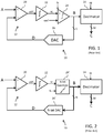
- Figure 1 shows a time domain block diagram of a conventional sigma-delta analog-to-digital converter circuit 10.
- the circuit 10 includes a first order sigma-delta modulator circuit 12 having an input configured to receive an analog input signal A and an output configured to generate a digital output signal B comprised of a pulse density modulated pulse stream of 1-bit codes.
- the ratio formed by a count of the number of pulses in the pulse stream of the signal B divided by a total number of samples (set by a sampling rate fs) of the input signal A over a known time interval represents the instantaneous magnitude of the input signal A.
- the circuit 10 further includes a decimator circuit 14 that accumulates and averages the pulses in the pulse stream of the digital output signal B to generate a digital signal C comprised of a stream of multi-bit (M-bit, where M>>1) digital words at a data rate set by a decimation rate fd, where fd ⁇ fs (referred to in the art as oversampling).
- M-bit multi-bit
- fd decimation rate
- the first order sigma-delta modulator circuit 12 comprises a difference amplifier 20 (or summation circuit) having a first (non-inverting) input that receives the analog input signal A and a second (inverting) input that receives an analog feedback signal D.
- the analog difference signal vdif is integrated by an integrator circuit 22 to generate a change signal vc having a slope and magnitude that is dependent on the sign and magnitude of the analog difference signal vdif.
- a voltage comparator circuit 24 samples the change signal vc at the sampling rate fs and compares each sample of the change signal vc to a reference signal vref to generate a corresponding the single bit pulse of the digital output signal B (where the single bit has a first logic state if vc ⁇ vref and has a second logic state if vc ⁇ vref).
- the voltage comparator circuit 24 effectively operates as a single bit quantization circuit.
- a single bit digital-to-analog converter (DAC) circuit 26 then converts the logic state of the digital output signal B to a corresponding analog voltage level for the analog feedback signal D.
- the sigma-delta modulator circuit 12 with a multi-bit quantization (for example, N bits, where 1 ⁇ N ⁇ M) as shown by Figure 2 .
- This circuit implementation requires an N-bit quantization circuit 24' and an N-bit DAC circuit 26' in the feedback loop.
- the quantization circuit 24' samples the change signal vc at the sampling rate fs and generates for each sample a corresponding N-bit code word for the digital output signal B.
- the DAC circuit 26' converts the N-bit code word of the digital output signal B to a corresponding analog voltage level for the analog feedback signal D.
- the decimator circuit 14 accumulates and averages the N-bit code words in the stream of the digital output signal B to generate a digital signal C comprised of the stream of multi-bit (M-bit, where M>>N) digital words at a data rate set by a decimation rate fd.
- M multi-bit
- the use of multi-bit quantization presents a number of advantages including: permitting operation of the modulator to achieve a given resolution using a lower sampling rate fs; or permitting operation of the modulator to achieve a higher resolution for a given sampling rate fs.
- a key characteristic of the sigma-delta modulator circuit 12 is its ability to push the quantization noise due to operation of the quantization circuit 24, 24' to higher frequencies away from the signal of interest. This is known in the art as noise shaping.
- the decimator circuit 14 can then be implemented with a low-pass filtering characteristic to substantially remove the high frequency components of the shaped quantization noise.
- the selecting signals unary thermometric in this embodiment
- the ideal DAC will output an analog voltage of 0.4 V (i.e., the summation of four selected unit elements of 0.1 V each).
- Equation 2 On comparing the Equation 2 with the ideal DAC output Equation 1, the second term in Equation 2 is the error introduced in the DAC and is referred as DAC error (or mismatch error).
- DAC error or mismatch error.
- the non-linearity also modulates the quantization noise of the quantization circuit 24' into the signal band resulting in a degraded signal-to-noise ratio (SNR).
- SNR signal-to-noise ratio
- a sigma-delta modulator comprises: a differencing circuit having a first input configured to receive an input signal and a second input configured to receive a feedback signal and an output configured to generate a difference signal; a K-th order loop filter circuit configured to filter the difference signal and generate a change signal; an N-bit quantization circuit configured to sample the change signal at a sampling frequency rate, quantize the sampled change signal and generate a stream of N-bit code words; an N-bit digital-to-analog converter (DAC) circuit configured to convert the stream of N-bit code words to generate the feedback signal, wherein the N-bit DAC circuit has a non-ideal operation due to mismatch error; and a digital DAC copy circuit that provides a digital replication of the N-bit DAC circuit, said digital replication accounting for the non-ideal operation of the N-bit DAC circuit due to mismatch error, the digital DAC copy circuit configured to convert the stream of N-bit code words to output a stream of P-bit code words, where P>N,
- a sigma-delta modulator comprises: a differencing circuit having a first input configured to receive an input signal and a second input configured to receive a feedback signal and an output configured to generate a difference signal; a K-th order loop filter circuit configured to filter the difference signal and generate a change signal; an N-bit quantization circuit configured to sample the change signal at a sampling frequency rate, quantize the sampled change signal and generate a stream of N-bit code words; an N-bit digital-to-analog converter (DAC) circuit configured to convert the stream of N-bit code words to generate the feedback signal, wherein the N-bit DAC circuit has a non-ideal operation due to mismatch error; and a digital DAC copy circuit that provides a digital replication of the N-bit DAC circuit, said digital replication accounting for the non-ideal operation of the N-bit DAC circuit due to mismatch error, the digital DAC copy circuit configured to convert the stream of N-bit code words to output a stream of P-bit code words, where P>N,
- FIG. 3 shows a block diagram of a sigma-delta analog-to-digital converter circuit 110 with multi-bit quantization and feedback digital-to-analog converter (DAC) mismatch correction.
- the circuit 110 includes an N-bit sigma-delta modulator circuit 112 having an input configured to receive an analog input signal A and an output configured to generate a digital output signal B comprised of a stream of N-bit code words.
- the sigma-delta modulator circuit 112 comprises a difference amplifier 120 (i.e., summation circuit) having a first (non-inverting) input that receives the analog input signal A and a second (inverting) input that receives an analog feedback signal D.
- the analog difference signal vdif is integrated by a K-order loop filter 116 (using, for example, K integrator circuits 122) to generate a change signal vc having a slope and magnitude that is dependent on the sign and magnitude of the analog difference signal vdif.
- An N-bit quantization circuit 124 samples the change signal vc at the sampling rate fs and generates for each sample a corresponding N-bit code word of the digital output signal B.
- An N-bit digital-to-analog converter (DAC) circuit 126 in the feedback loop converts the N-bit code word of the digital output signal B to a corresponding voltage level for the analog feedback signal D.
- DAC digital-to-analog converter
- the sigma-delta modulator circuit 112 implements a loop filter 116 with a K-order integration circuit implementation.
- K 1 as there is only one integration shown (with integrator 122) in the loop filter 116, but it will be understood that this is by way of example only, and K may equal 2, 3 or more as needed by the desired noise shaping and circuit application.
- K may equal 2, 3 or more as needed by the desired noise shaping and circuit application.
- the stream of N-bit code words for the digital output signal B produced by the N-bit quantization circuit 124 are input to the N-bit DAC circuit 126 in the feedback path and are further input to a digital DAC copy circuit 118.
- the digital DAC copy circuit 118 is calibrated (in a manner to be discussed in detail herein) to digitally model the operation of the feedback N-bit DAC circuit 126.
- the digital output signal B from the N-bit quantization circuit 124 is subjected to quantization error along with the desired signal.
- any signal or noise entity injected at any point in the feedback loop of the modulator 112 will be high passed (i.e., noise shaped) by the noise transfer function of the modulator.
- the effect of this high pass noise shaping of the injected signal or noise is visible just after the point of injection.
- the quantization error injected into the feedback loop by the N-bit quantization circuit 124 is advantageously noise shaped (high passed) by the modulator 112 at the digital output signal B with a high pass function (1-z -1 ) K proportional to the order (K) of the modulator.
- the digital output signal B is processed by the N-bit DAC circuit 126 of the modulator 112.
- This N-bit DAC circuit 126 has a non-ideal operation due at least in part to a mismatch between its building blocks (unit elements, as discussed above) as a result of circuit fabrication imperfections.
- a DAC having a non-ideal operation can be modelled as an ideal DAC followed by an error signal source injecting the mismatch error (see, also, Equation 2).
- the mismatch error due to operation of the N-bit DAC circuit 126 is high passed (i.e., noise shaped) by the noise transfer function of the modulator.
- the effect of this high pass noise shaping of the injected mismatch error is visible just after the point of injection. So, the mismatch error injected into the feedback loop by the N-bit DAC circuit 126 is advantageously noise shaped (high passed) by the modulator 112 at the analog feedback signal D with a high pass function (1-z -1 ) K proportional to the order (K) of the modulator.
- the digital DAC copy circuit 118 provides a digital replication of the analog N-bit DAC circuit 126, that replication specifically accounting for the non-ideal operation of the N-bit DAC circuit 126 due to unit element mismatch. More specifically, the digital DAC copy circuit 118 is programmed with a plurality of digital code words that are directly proportional to the value of the mismatched unit elements of the analog N-bit DAC circuit 126. In other words, digital codes corresponding to the analog value of the unit element error e i .
- the digital code words can be of any selected precision P, and are determined using a calibration process (to be discussed in detail herein).
- the digital model provided by the digital DAC copy circuit 118 is substantially identical to the non-ideal actual operation of the analog N-bit DAC circuit 126, then the digital signal E output from the digital DAC copy circuit 118 will be functionally equivalent to the analog feedback signal D output from the analog N-bit DAC circuit 126.
- “functionally equivalent” means that an analog conversion of the digital value for the digital signal E generated in response to signal B by the digital DAC copy circuit 118 is substantially equal to the corresponding analog value for the analog feedback signal D generated in response to that same signal B.
- the digital signal E output by the digital DAC copy circuit 118 comprises a stream of P-bit code words (where P>N, the higher resolution provide by P bits being necessary to provide fractional components necessary to account for effects of the mismatch error).
- P-N the difference in bits
- the digital signal E output from the digital DAC copy circuit 118 will be a code word with a precision of P-bits formed by summing the N-bit digital code for 2* ⁇ (i.e., the ideal response) plus the digital code for ⁇ times the sum of the programmed digital code words for the unit element errors e 1 and e 2 (i.e., ⁇ ( e 1 + e 2 )) which is the introduced mismatch error.
- the calibration process can be used to generate a look-up table that is programmed into the digital DAC copy circuit 118 and used to translate the received N-bit digital values generated by the N-bit quantization circuit 124 into corresponding P-bit digital values for the digital signal E.
- translation techniques other than use of a look-up table could be implemented by the digital DAC copy circuit 118.
- a summation node could be utilized to selectively sum the estimated mismatch codes of the model depending on the received unary inputs. This could be the preferred method if inputs other than thermometric codes (e.g., scrambled unary codes) are applied as input to the digital DAC copy circuit 118.
- thermometric codes e.g., scrambled unary codes
- a multiply-add structure could instead be used.
- the circuit 110 further includes a decimator circuit 114 that accumulates and averages the P-bit code words in the stream of the digital output signal E to generate a digital signal C comprised of a stream of multi-bit (M-bit) digital words at a data rate set by a decimation rate fd, where fd ⁇ fs and 1 ⁇ N ⁇ P ⁇ M.
- the decimator circuit 114 implements a low pass filtering to effectively remove the high-passed signal components of the quantization error and mismatch error.
- em(n) be the mismatch error introduced by the operation of the DAC circuit 126 due to the existence of unequal analog output steps, where n is the sampling index.
- the analog feedback signal D may accordingly be given in the Z-domain by: v n + em n 1 ⁇ z ⁇ 1 K where: v(n) is the ideal output of the quantization circuit 124.
- eq(n) be the quantization error introduced by the operation of the n-bit quantization circuit 124.
- the digital output signal B may be given in the Z-domain by: v n + eq n * 1 ⁇ z ⁇ 1 K
- the digital signal E may be given by: v n + eq n + em n 1 ⁇ z ⁇ 1 K
- FIG. 4 additionally shows the calibration circuitry 200 for the N-bit sigma-delta modulator circuit 112 that is used to program the digital DAC copy circuit 118 with a digital model of the feedback N-bit DAC circuit 126.
- a first multiplexer circuit 202 has a first input coupled to receive the digital output signal B produced by the N-bit quantization circuit 124 and a second input configured to receive a digital code word calibration signal 204.
- the selection operation of the first multiplexer circuit 202 is controlled by a selection control signal 206 such that when the selection control signal 206 is in a first logic state the digital output signal B is passed by the first multiplexer circuit 202 to the feedback N-bit DAC circuit 126 and when the selection control signal 206 is in a second logic state the digital code word calibration signal 204 is passed by the first multiplexer circuit 202 to the feedback N-bit DAC circuit 126.
- a second multiplexer circuit 212 has a first input coupled to receive a digital zero (or null) input signal 208 and a second input configured to receive the digital output signal B produced by the N-bit quantization circuit 124.
- the selection operation of the second multiplexer circuit 212 is also controlled by the selection control signal 206 such that when the selection control signal 206 is in the first logic state the digital zero (or null) input signal 208 is passed by the second multiplexer circuit 212 to an N-bit estimation DAC circuit 216 and when the selection control signal 206 is in a second logic state the digital output signal B is passed by the second multiplexer circuit 212 to the N-bit estimation DAC circuit 216.
- the N-bit estimation DAC circuit 216 is configured to have a linear response (i.e., none to negligible mismatch error) through the use of dynamic element matching (DEM) techniques known to those skilled in the art.
- DEM dynamic element matching
- those skilled in the art understand that the DEM technique works well for low frequency band limited signals, and such signals are the signals being processed during calibration mode.
- the DEM is not so effective for high frequency wide bandwidth signals, such as with the input signal A, and thus use of the DEM technique for the feedback N-bit DAC circuit 126 is not a particularly effective or economical solution.
- a differencing (summation) circuit 220 subtracts the analog signal 222 output by the N-bit estimation DAC circuit 216 from the analog signal 224 output by the feedback N-bit DAC circuit 126 to generate the analog feedback signal D.
- a control and processing circuit 240 for the calibration operation has an input coupled to receive the digital output signal B produced by the N-bit quantization circuit 124.
- the control and processing circuit 240 further generates the selection control signal 206, as well as the digital code word signal 204 and the digital zero (or null) input signal 208, and can further apply a selected input signal A during calibration mode.
- the control and processing circuit 240 operates in calibration mode to identify the mismatch error of the feedback N-bit DAC circuit 126 from the received digital output signal B and program the digital DAC copy circuit 118 through signal 242 to digitally model the operation of the feedback N-bit DAC circuit 126.
- the control and processing circuit 240 asserts the selection control signal 206 in the first logic state so that the digital output signal B is passed by the first multiplexer circuit 202 to the feedback N-bit DAC circuit 126 and the zero (or null) input signal 208 is passed by the second multiplexer circuit 212.
- the circuit is configured for operation in the manner shown by Figure 3 because the analog signal 222 output by the N-bit estimation DAC circuit 216 is zero.
- the control and processing circuit 240 asserts the selection control signal 206 in the second logic state so that the digital code word calibration signal 204 is passed by the first multiplexer circuit 202 to the feedback N-bit DAC circuit 126 and the digital output signal B is passed by the second multiplexer circuit 212 to the N-bit estimation DAC circuit 216.
- the control and processing circuit 240 applies a zero voltage input as the analog input signal A.
- the feedback N-bit DAC circuit 126 converts the digital code word calibration signal 204 provided by the control and processing circuit 240 to generate analog signal 224 and the bit estimation DAC circuit 216 converts the digital output signal B to generate analog signal 222.
- the analog signal 223 is summed with the analog signal 224 to complete the sigma-delta loop and generate the analog feedback signal D.
- the digital output signal B is then processed by the control and processing circuit 240 using low pass filtering and decimation (similar to that performed by the decimator 114) in order to digitally measure the analog voltage output from the analog N-bit DAC circuit 126 in response to the applied digital code word calibration signal 204.
- the calibration mode is using the modulator 112 to measure only the operating characteristics of the N-bit DAC circuit 126.
- the control and processing circuit 240 will apply values for the digital code word calibration signal 204 during the calibration operation which correspond to all possible digital code words generated by the N-bit quantization circuit 124 for the digital output signal B.
- the generated digital code words for the unit element are programmed into the digital DAC copy circuit 118 through signal 242 in order to digitally model the operation of the feedback N-bit DAC circuit 126.
Landscapes
- Engineering & Computer Science (AREA)
- Theoretical Computer Science (AREA)
- Physics & Mathematics (AREA)
- Nonlinear Science (AREA)
- Compression, Expansion, Code Conversion, And Decoders (AREA)
Abstract
A sigma-delta modulator includes an N-bit quantization circuit that generates a stream of N-bit code words and a feedback signal path with an N-bit DAC circuit, having a non-ideal operation due to mismatch error, that converts the stream of N-bit code words to generate a feedback signal. A digital DAC copy circuit provides a digital replication of the N-bit DAC circuit. The digital replication accounts for the non-ideal operation of the N-bit DAC circuit 126 due to mismatch error, and converts the stream of N-bit code words to generate a stream of P-bit code words, where P>N, that are functionally equivalent to the feedback signal output from the N-bit DAC circuit.
Description
- This application claims priority from United States Provisional Application for Patent No.
62/859,531 filed June 10, 2019 - Embodiments generally relate to an analog-to-digital converter circuit and, in particular, to a sigma-delta analog-to-digital converter circuit.
-
Figure 1 shows a time domain block diagram of a conventional sigma-delta analog-to-digital converter circuit 10. Thecircuit 10 includes a first order sigma-delta modulator circuit 12 having an input configured to receive an analog input signal A and an output configured to generate a digital output signal B comprised of a pulse density modulated pulse stream of 1-bit codes. The ratio formed by a count of the number of pulses in the pulse stream of the signal B divided by a total number of samples (set by a sampling rate fs) of the input signal A over a known time interval represents the instantaneous magnitude of the input signal A. Thecircuit 10 further includes adecimator circuit 14 that accumulates and averages the pulses in the pulse stream of the digital output signal B to generate a digital signal C comprised of a stream of multi-bit (M-bit, where M>>1) digital words at a data rate set by a decimation rate fd, where fd<<fs (referred to in the art as oversampling). - The first order sigma-
delta modulator circuit 12 comprises a difference amplifier 20 (or summation circuit) having a first (non-inverting) input that receives the analog input signal A and a second (inverting) input that receives an analog feedback signal D. The difference amplifier 20 outputs an analog difference signal vdif in response to a difference between the analog input signal A and the analog feedback signal D (i.e., vdif(t) = A(t) - D(t)). The analog difference signal vdif is integrated by anintegrator circuit 22 to generate a change signal vc having a slope and magnitude that is dependent on the sign and magnitude of the analog difference signal vdif. Avoltage comparator circuit 24 samples the change signal vc at the sampling rate fs and compares each sample of the change signal vc to a reference signal vref to generate a corresponding the single bit pulse of the digital output signal B (where the single bit has a first logic state if vc≥vref and has a second logic state if vc<vref). Thevoltage comparator circuit 24 effectively operates as a single bit quantization circuit. A single bit digital-to-analog converter (DAC)circuit 26 then converts the logic state of the digital output signal B to a corresponding analog voltage level for the analog feedback signal D. - It is possible to instead implement the sigma-
delta modulator circuit 12 with a multi-bit quantization (for example, N bits, where 1<N<<M) as shown byFigure 2 . This circuit implementation requires an N-bit quantization circuit 24' and an N-bit DAC circuit 26' in the feedback loop. The quantization circuit 24' samples the change signal vc at the sampling rate fs and generates for each sample a corresponding N-bit code word for the digital output signal B. The DAC circuit 26' converts the N-bit code word of the digital output signal B to a corresponding analog voltage level for the analog feedback signal D. Thedecimator circuit 14 accumulates and averages the N-bit code words in the stream of the digital output signal B to generate a digital signal C comprised of the stream of multi-bit (M-bit, where M>>N) digital words at a data rate set by a decimation rate fd. In an example, N=3-5 and M=12-16. The use of multi-bit quantization presents a number of advantages including: permitting operation of the modulator to achieve a given resolution using a lower sampling rate fs; or permitting operation of the modulator to achieve a higher resolution for a given sampling rate fs. - A key characteristic of the sigma-
delta modulator circuit 12 is its ability to push the quantization noise due to operation of thequantization circuit 24, 24' to higher frequencies away from the signal of interest. This is known in the art as noise shaping. Thedecimator circuit 14 can then be implemented with a low-pass filtering characteristic to substantially remove the high frequency components of the shaped quantization noise. - The use of multi-bit quantization in sigma-delta modulator circuits, however, is difficult because the inherent non-linearity present in the operation of the DAC circuit 26' in the feedback loop translates directly into non-linearity of the
entire modulator 12. This non-linearity is due, for example, to the existence of unequal analog output steps (i.e., mismatch error) for the multi-bit DAC circuit. - The output of an ideal DAC is the sum of the outputs of its actuated unit elements:

where: bi (k) for (i=1, 2, ... U) is referred to as the selecting signals (unary thermometric in this embodiment) depending on DAC precision. In case of an N=4 bit DAC, there are U=(24-1)=15 unit elements, and k in bi (k) is the kth input; and where Δ equals the quantization step. As an example, for Δ=0.1V and bi (k)=<111100000000000>, the ideal DAC will output an analog voltage of 0.4 V (i.e., the summation of four selected unit elements of 0.1 V each). - In practice, the current sources used in the DAC are not ideal in nature resulting in deviations from their ideal value. Assume ei (i=1, 2, ..., U) are the values of normalized deviations of the unit elements outputs from their mean value (referred to as unit element errors). Thus, the output of each unit element can be represented as Δ (1 + ei ). The output of a non-ideal DAC is then:

- On comparing the Equation 2 with the ideal
DAC output Equation 1, the second term in Equation 2 is the error introduced in the DAC and is referred as DAC error (or mismatch error). Using the same example with Δ=0.1V and bi (k)=<111100000000000>, when the first four DAC elements are summed, their errors are also summed and presented at the output to produce an analog voltage of 0.1*((1+e 1)+(1+e 2)+(1+e 3)+(1+e 4)). - The DAC error is basically then the sum of the selecting signals (i.e., bi (k)) multiplied by corresponding errors (ei ) over U signals:

- As a result of the non-linearity introduced in the analog output of the DAC by the DAC error, a distorted modulator output is produced. The non-linearity also modulates the quantization noise of the quantization circuit 24' into the signal band resulting in a degraded signal-to-noise ratio (SNR).
- In order to take advantage of the benefits of multi-bit quantization in sigma-delta modulator circuits, it is necessary to estimate the inherent non-linearity present in the operation of the multi-bit DAC circuit and apply a correction to nullify its effects.
- In an embodiment, a sigma-delta modulator comprises: a differencing circuit having a first input configured to receive an input signal and a second input configured to receive a feedback signal and an output configured to generate a difference signal; a K-th order loop filter circuit configured to filter the difference signal and generate a change signal; an N-bit quantization circuit configured to sample the change signal at a sampling frequency rate, quantize the sampled change signal and generate a stream of N-bit code words; an N-bit digital-to-analog converter (DAC) circuit configured to convert the stream of N-bit code words to generate the feedback signal, wherein the N-bit DAC circuit has a non-ideal operation due to mismatch error; and a digital DAC copy circuit that provides a digital replication of the N-bit DAC circuit, said digital replication accounting for the non-ideal operation of the N-bit DAC circuit due to mismatch error, the digital DAC copy circuit configured to convert the stream of N-bit code words to output a stream of P-bit code words, where P>N, that are functionally equivalent to the feedback signal output from the N-bit DAC circuit.
- In an embodiment, a sigma-delta modulator comprises: a differencing circuit having a first input configured to receive an input signal and a second input configured to receive a feedback signal and an output configured to generate a difference signal; a K-th order loop filter circuit configured to filter the difference signal and generate a change signal; an N-bit quantization circuit configured to sample the change signal at a sampling frequency rate, quantize the sampled change signal and generate a stream of N-bit code words; an N-bit digital-to-analog converter (DAC) circuit configured to convert the stream of N-bit code words to generate the feedback signal, wherein the N-bit DAC circuit has a non-ideal operation due to mismatch error; and a digital DAC copy circuit that provides a digital replication of the N-bit DAC circuit, said digital replication accounting for the non-ideal operation of the N-bit DAC circuit due to mismatch error, the digital DAC copy circuit configured to convert the stream of N-bit code words to output a stream of P-bit code words, where P>N, each P-bit code word comprising a combination of: a first digital code corresponding to an ideal output of the N-bit DAC circuit in response to the N-bit code word; a second digital code corresponding to unit element error of the N-bit DAC circuit in response to the N-bit code word.
- For a better understanding of the embodiments, reference will now be made by way of example only to the accompanying figures in which:
-
Figure 1 is a block diagram of a conventional sigma-delta analog-to-digital converter circuit with single bit quantization; -
Figure 2 is a block diagram of a conventional sigma-delta analog-to-digital converter circuit with multi-bit quantization; -
Figure 3 is a block diagram of a sigma-delta analog-to-digital converter circuit with multi-bit quantization and feedback digital-to-analog converter mismatch correction; and -
Figure 4 is a block diagram showing configuration circuitry for the circuit ofFigure 3 . - Reference is now made to
Figure 3 which shows a block diagram of a sigma-delta analog-to-digital converter circuit 110 with multi-bit quantization and feedback digital-to-analog converter (DAC) mismatch correction. Thecircuit 110 includes an N-bit sigma-delta modulator circuit 112 having an input configured to receive an analog input signal A and an output configured to generate a digital output signal B comprised of a stream of N-bit code words. The sigma-delta modulator circuit 112 comprises a difference amplifier 120 (i.e., summation circuit) having a first (non-inverting) input that receives the analog input signal A and a second (inverting) input that receives an analog feedback signal D. The difference amplifier 20 outputs an analog difference signal vdif in response to a difference between the analog input signal A and the analog feedback signal D (where vdif(t) = A(t) - D(t)). The analog difference signal vdif is integrated by a K-order loop filter 116 (using, for example, K integrator circuits 122) to generate a change signal vc having a slope and magnitude that is dependent on the sign and magnitude of the analog difference signal vdif. An N-bit quantization circuit 124 samples the change signal vc at the sampling rate fs and generates for each sample a corresponding N-bit code word of the digital output signal B. An N-bit digital-to-analog converter (DAC)circuit 126 in the feedback loop converts the N-bit code word of the digital output signal B to a corresponding voltage level for the analog feedback signal D. - The sigma-
delta modulator circuit 112 implements aloop filter 116 with a K-order integration circuit implementation. In the illustration ofFigure 1 , K=1 as there is only one integration shown (with integrator 122) in theloop filter 116, but it will be understood that this is by way of example only, and K may equal 2, 3 or more as needed by the desired noise shaping and circuit application. Those skilled in the know how to implement a K>1order loop filter 116 for the sigma-delta modulator circuit 112. - It is known in the prior art to address the issue of the feedback DAC mismatch error by applying correction at the DAC circuit itself. See, for example, United States Patent No.
10,148,278 9,438,266 digital converter circuit 110 ofFigure 3 uses a different solution to the issue of compensating for feedback DAC mismatch error. - The stream of N-bit code words for the digital output signal B produced by the N-
bit quantization circuit 124 are input to the N-bit DAC circuit 126 in the feedback path and are further input to a digitalDAC copy circuit 118. In this context, the digitalDAC copy circuit 118 is calibrated (in a manner to be discussed in detail herein) to digitally model the operation of the feedback N-bit DAC circuit 126. In other words, to digitally model the ideal DAC operation plus the DAC error introduced by the non-linear operation of the unit elements:
- As previously noted, the digital output signal B from the N-
bit quantization circuit 124 is subjected to quantization error along with the desired signal. Those skilled in the art understand that any signal or noise entity injected at any point in the feedback loop of themodulator 112 will be high passed (i.e., noise shaped) by the noise transfer function of the modulator. The effect of this high pass noise shaping of the injected signal or noise is visible just after the point of injection. So, the quantization error injected into the feedback loop by the N-bit quantization circuit 124 is advantageously noise shaped (high passed) by themodulator 112 at the digital output signal B with a high pass function (1-z-1)K proportional to the order (K) of the modulator. - On further traversing the feedback loop, the digital output signal B is processed by the N-
bit DAC circuit 126 of themodulator 112. This N-bit DAC circuit 126 has a non-ideal operation due at least in part to a mismatch between its building blocks (unit elements, as discussed above) as a result of circuit fabrication imperfections. A DAC having a non-ideal operation can be modelled as an ideal DAC followed by an error signal source injecting the mismatch error (see, also, Equation 2). As with the case of the N-bit quantization circuit 124 discussed above, with the N-bit DAC circuit 126 inserted in the feedback loop of themodulator 112, the mismatch error due to operation of the N-bit DAC circuit 126 is high passed (i.e., noise shaped) by the noise transfer function of the modulator. The effect of this high pass noise shaping of the injected mismatch error is visible just after the point of injection. So, the mismatch error injected into the feedback loop by the N-bit DAC circuit 126 is advantageously noise shaped (high passed) by themodulator 112 at the analog feedback signal D with a high pass function (1-z-1)K proportional to the order (K) of the modulator. - The digital
DAC copy circuit 118 provides a digital replication of the analog N-bit DAC circuit 126, that replication specifically accounting for the non-ideal operation of the N-bit DAC circuit 126 due to unit element mismatch. More specifically, the digitalDAC copy circuit 118 is programmed with a plurality of digital code words that are directly proportional to the value of the mismatched unit elements of the analog N-bit DAC circuit 126. In other words, digital codes corresponding to the analog value of the unit element error ei . The digital code words can be of any selected precision P, and are determined using a calibration process (to be discussed in detail herein). It will be appreciated that if the digital model provided by the digitalDAC copy circuit 118 is substantially identical to the non-ideal actual operation of the analog N-bit DAC circuit 126, then the digital signal E output from the digitalDAC copy circuit 118 will be functionally equivalent to the analog feedback signal D output from the analog N-bit DAC circuit 126. In this context, "functionally equivalent" means that an analog conversion of the digital value for the digital signal E generated in response to signal B by the digitalDAC copy circuit 118 is substantially equal to the corresponding analog value for the analog feedback signal D generated in response to that same signal B. The digital signal E output by the digitalDAC copy circuit 118 comprises a stream of P-bit code words (where P>N, the higher resolution provide by P bits being necessary to provide fractional components necessary to account for effects of the mismatch error). The difference in bits (P-N) defines the degree of substantial equality that is achievable. - The operation of the digital
DAC copy circuit 118 may be better understood through the use of an example. Assume that the digital output signal B has four bits (i.e., N=4) and for one specific case has a digital value of <0010> output from the N-bit quantization circuit 124 resulting in a selection signal of <110000000000000>. If the analog N-bit DAC circuit 126 had an ideal functional operation, the analog voltage for the analog feedback signal D output from the analog N-bit DAC circuit 126 would have a value of 2*Δ. However, due to mismatch error, the voltage of the generated analog feedback signal D output from the analog N-bit DAC circuit 126 instead has a value of 2*Δ+e 1Δ+e 2Δ. The calibration process to be described herein digitally measures the analog voltage output from the analog N-bit DAC circuit 126 for each possible code word for the digital output signal B, and from those measurements determines the error ei for each unit element (i=1, 2, ... U). A digital code word corresponding to each determined unit element error is then produced and programmed into the digitalDAC copy circuit 118. So, with consideration to the same example where the digital output signal B from the N-bit quantization circuit 124 has a digital value of <0010>, the digital signal E output from the digitalDAC copy circuit 118 will be a code word with a precision of P-bits formed by summing the N-bit digital code for 2*Δ (i.e., the ideal response) plus the digital code for Δ times the sum of the programmed digital code words for the unit element errors e 1 and e 2 (i.e., Δ(e 1+e 2)) which is the introduced mismatch error. - It will be noted that the calibration process can be used to generate a look-up table that is programmed into the digital
DAC copy circuit 118 and used to translate the received N-bit digital values generated by the N-bit quantization circuit 124 into corresponding P-bit digital values for the digital signal E. It will be understood that translation techniques other than use of a look-up table could be implemented by the digitalDAC copy circuit 118. For example, a summation node could be utilized to selectively sum the estimated mismatch codes of the model depending on the received unary inputs. This could be the preferred method if inputs other than thermometric codes (e.g., scrambled unary codes) are applied as input to the digitalDAC copy circuit 118. In rare instances of design where inputs to the digitalDAC copy circuit 118 are binary or two's complement, a multiply-add structure could instead be used. - The
circuit 110 further includes adecimator circuit 114 that accumulates and averages the P-bit code words in the stream of the digital output signal E to generate a digital signal C comprised of a stream of multi-bit (M-bit) digital words at a data rate set by a decimation rate fd, where fd<<fs and 1<N<P<<M. Thedecimator circuit 114 implements a low pass filtering to effectively remove the high-passed signal components of the quantization error and mismatch error. - Let em(n) be the mismatch error introduced by the operation of the
DAC circuit 126 due to the existence of unequal analog output steps, where n is the sampling index. The analog feedback signal D may accordingly be given in the Z-domain by:
where: v(n) is the ideal output of thequantization circuit 124. - Furthermore, let eq(n) be the quantization error introduced by the operation of the n-
bit quantization circuit 124. The digital output signal B may be given in the Z-domain by:
- The digital signal E may be given by:

- It will be noted that both the quantization error and the mismatch error have been high pass noise shaped.
- Reference is now made to
Figure 4 which additionally shows thecalibration circuitry 200 for the N-bit sigma-delta modulator circuit 112 that is used to program the digitalDAC copy circuit 118 with a digital model of the feedback N-bit DAC circuit 126. Afirst multiplexer circuit 202 has a first input coupled to receive the digital output signal B produced by the N-bit quantization circuit 124 and a second input configured to receive a digital codeword calibration signal 204. The selection operation of thefirst multiplexer circuit 202 is controlled by aselection control signal 206 such that when theselection control signal 206 is in a first logic state the digital output signal B is passed by thefirst multiplexer circuit 202 to the feedback N-bit DAC circuit 126 and when theselection control signal 206 is in a second logic state the digital codeword calibration signal 204 is passed by thefirst multiplexer circuit 202 to the feedback N-bit DAC circuit 126. - A
second multiplexer circuit 212 has a first input coupled to receive a digital zero (or null)input signal 208 and a second input configured to receive the digital output signal B produced by the N-bit quantization circuit 124. The selection operation of thesecond multiplexer circuit 212 is also controlled by theselection control signal 206 such that when theselection control signal 206 is in the first logic state the digital zero (or null)input signal 208 is passed by thesecond multiplexer circuit 212 to an N-bitestimation DAC circuit 216 and when theselection control signal 206 is in a second logic state the digital output signal B is passed by thesecond multiplexer circuit 212 to the N-bitestimation DAC circuit 216. - The N-bit
estimation DAC circuit 216 is configured to have a linear response (i.e., none to negligible mismatch error) through the use of dynamic element matching (DEM) techniques known to those skilled in the art. In this regard, those skilled in the art understand that the DEM technique works well for low frequency band limited signals, and such signals are the signals being processed during calibration mode. The DEM is not so effective for high frequency wide bandwidth signals, such as with the input signal A, and thus use of the DEM technique for the feedback N-bit DAC circuit 126 is not a particularly effective or economical solution. - A differencing (summation)
circuit 220 subtracts theanalog signal 222 output by the N-bitestimation DAC circuit 216 from theanalog signal 224 output by the feedback N-bit DAC circuit 126 to generate the analog feedback signal D. - A control and
processing circuit 240 for the calibration operation has an input coupled to receive the digital output signal B produced by the N-bit quantization circuit 124. The control andprocessing circuit 240 further generates theselection control signal 206, as well as the digital code word signal 204 and the digital zero (or null)input signal 208, and can further apply a selected input signal A during calibration mode. The control andprocessing circuit 240 operates in calibration mode to identify the mismatch error of the feedback N-bit DAC circuit 126 from the received digital output signal B and program the digitalDAC copy circuit 118 throughsignal 242 to digitally model the operation of the feedback N-bit DAC circuit 126. - When the N-bit sigma-
delta modulator circuit 112 is not being calibrated, the control andprocessing circuit 240 asserts theselection control signal 206 in the first logic state so that the digital output signal B is passed by thefirst multiplexer circuit 202 to the feedback N-bit DAC circuit 126 and the zero (or null)input signal 208 is passed by thesecond multiplexer circuit 212. In this mode, the circuit is configured for operation in the manner shown byFigure 3 because theanalog signal 222 output by the N-bitestimation DAC circuit 216 is zero. - When the N-bit sigma-
delta modulator circuit 112 is being calibrated, the control andprocessing circuit 240 asserts theselection control signal 206 in the second logic state so that the digital codeword calibration signal 204 is passed by thefirst multiplexer circuit 202 to the feedback N-bit DAC circuit 126 and the digital output signal B is passed by thesecond multiplexer circuit 212 to the N-bitestimation DAC circuit 216. In this calibration configuration, the control andprocessing circuit 240 applies a zero voltage input as the analog input signal A. The feedback N-bit DAC circuit 126 converts the digital codeword calibration signal 204 provided by the control andprocessing circuit 240 to generateanalog signal 224 and the bitestimation DAC circuit 216 converts the digital output signal B to generateanalog signal 222. The analog signal 223 is summed with theanalog signal 224 to complete the sigma-delta loop and generate the analog feedback signal D. The digital output signal B is then processed by the control andprocessing circuit 240 using low pass filtering and decimation (similar to that performed by the decimator 114) in order to digitally measure the analog voltage output from the analog N-bit DAC circuit 126 in response to the applied digital codeword calibration signal 204. In other words, the calibration mode is using themodulator 112 to measure only the operating characteristics of the N-bit DAC circuit 126. - The control and
processing circuit 240 will apply values for the digital codeword calibration signal 204 during the calibration operation which correspond to all possible digital code words generated by the N-bit quantization circuit 124 for the digital output signal B. Through processing of the digitally measured analog voltage outputs from the analog N-bit DAC circuit 126 in response to all possible digital code words, the control andprocessing circuit 240 can determine the error ei for each unit element (i=1, 2, ... U) of the analog N-bit DAC circuit 126 and generate the corresponding digital code words which provide a complete picture of the non-linear response of the feedback N-bit DAC circuit 126. The generated digital code words for the unit element are programmed into the digitalDAC copy circuit 118 throughsignal 242 in order to digitally model the operation of the feedback N-bit DAC circuit 126. - While the invention has been illustrated and described in detail in the drawings and foregoing description, such illustration and description are considered illustrative or exemplary and not restrictive; the invention is not limited to the disclosed embodiments. Other variations to the disclosed embodiments can be understood and effected by those skilled in the art in practicing the claimed invention, from a study of the drawings, the disclosure, and the appended claims.
Claims (19)
- A sigma-delta modulator, comprising:a differencing circuit having a first input configured to receive an input signal and a second input configured to receive a feedback signal and an output configured to generate a difference signal;a K-th order loop filter circuit configured to filter the difference signal and generate a change signal;an N-bit quantization circuit configured to sample the change signal at a sampling frequency rate, quantize the sampled change signal and generate a stream of N-bit code words;an N-bit digital-to-analog converter (DAC) circuit configured to convert the stream of N-bit code words to generate the feedback signal, wherein the N-bit DAC circuit has a non-ideal operation due to mismatch error; anda digital DAC copy circuit that provides a digital replication of the N-bit DAC circuit, said digital replication accounting for the non-ideal operation of the N-bit DAC circuit due to mismatch error, the digital DAC copy circuit configured to convert the stream of N-bit code words to output a stream of P-bit code words, where P>N, that are functionally equivalent to the feedback signal output from the N-bit DAC circuit.
- The circuit of claim 1, wherein noise associated with the mismatch error is high pass noise shaped, further including a low pass filter configured to filter out high frequency components of the high pass noise shaped mismatch error.
- The circuit of claim 2, where the low pass filter is implemented by a decimation circuit configured to decimate the stream of P-bit code words at a decimation frequency rate to generate a stream of M-bit words, where M>P.
- The circuit of claim 1, further comprising a decimation circuit configured to decimate the stream of P-bit code words at a decimation frequency rate to generate a stream of M-bit words, where M>P.
- The circuit of claim 1, further comprising a calibration circuit configured to program the digital DAC copy circuit to provide the digital replication of the N-bit DAC circuit.
- The circuit of claim 5, wherein the calibration circuit comprises:an estimation N-bit DAC circuit;a further differencing circuit configured to generate the feedback signal as a difference between a first signal output from the N-bit DAC circuit and a second signal output from the estimation N-bit DAC circuit;a first multiplexing circuit having a first input configured to receive the stream of N-bit code words and a second input configured to receive an N-bit calibration code word, wherein an output of the first multiplexing circuit is applied to an input of the N-bit DAC circuit;a second multiplexing circuit having a first input configured to receive an N-bit null code word and a second input configured to receive the stream of N-bit code words, wherein an output of the second multiplexing circuit is applied to an input of the estimation N-bit DAC circuit; anda control and processing circuit having a first input configured to receive the stream of N-bit code words and an output configured to generate a programming signal for programming the digital DAC copy circuit, wherein the control and processing circuit controls the first and second multiplexing circuits in a calibration mode to select the second inputs, apply a value for the N-bit calibration code word, and process the stream of N-bit code words in response to the applied value to determine the mismatch error of the N-bit DAC circuit for the applied value in order to program the digital DAC copy circuit to provide the digital replication.
- The circuit of claim 6, wherein the control and processing circuit further controls the first and second multiplexing circuits in a normal operating mode to select the first inputs.
- The circuit of claim 6, wherein the control and processing circuit further applies a series of values for the N-bit calibration code word, and process the stream of N-bit code words in response to the applied series of values to determine the mismatch error of the N-bit DAC circuit for the applied series of values in order to program the digital DAC copy circuit to provide the digital replication.
- The circuit of claim 8, wherein the applied series of values include all possible values for input to the N-bit DAC circuit.
- The circuit of claim 1, wherein the digital DAC copy circuit includes a look-up table configured to translate N-bit code word generated by the N-bit quantization circuit to a corresponding P-bit code word for output by the digital DAC copy circuit.
- A sigma-delta modulator, comprising:a differencing circuit having a first input configured to receive an input signal and a second input configured to receive a feedback signal and an output configured to generate a difference signal;a K-th order loop filter circuit configured to filter the difference signal and generate a change signal;an N-bit quantization circuit configured to sample the change signal at a sampling frequency rate, quantize the sampled change signal and generate a stream of N-bit code words;an N-bit digital-to-analog converter (DAC) circuit configured to convert the stream of N-bit code words to generate the feedback signal, wherein the N-bit DAC circuit has a non-ideal operation due to mismatch error; anda digital DAC copy circuit that provides a digital replication of the N-bit DAC circuit, said digital replication accounting for the non-ideal operation of the N-bit DAC circuit due to mismatch error, the digital DAC copy circuit configured to convert the stream of N-bit code words to output a stream of P-bit code words, where P>N, each P-bit code word comprising a combination of:a first digital code corresponding to an ideal output of the N-bit DAC circuit in response to the N-bit code word;a second digital code corresponding to unit element error of the N-bit DAC circuit in response to the N-bit code word.
- The circuit of claim 11, wherein noise associated with the mismatch error is high pass noise shaped, further including a low pass filter configured to filter out high frequency components of the high pass noise shaped mismatch error.
- The circuit of claim 12, where the low pass filter is implemented by a decimation circuit configured to decimate the stream of P-bit code words at a decimation frequency rate to generate a stream of M-bit words, where M>P.
- The circuit of claim 11, further comprising a decimation circuit configured to decimate the stream of P-bit code words at a decimation frequency rate to generate a stream of M-bit words, where M>P.
- The circuit of claim 11, further comprising a calibration circuit configured to program the digital DAC copy circuit to provide the digital replication of the N-bit DAC circuit.
- The circuit of claim 15, wherein the calibration circuit comprises:an estimation N-bit DAC circuit;a further differencing circuit configured to generate the feedback signal as a difference between a first signal output from the N-bit DAC circuit and a second signal output from the estimation N-bit DAC circuit;a first multiplexing circuit having a first input configured to receive the stream of N-bit code words and a second input configured to receive an N-bit calibration code word, wherein an output of the first multiplexing circuit is applied to an input of the N-bit DAC circuit;a second multiplexing circuit having a first input configured to receive an N-bit null code word and a second input configured to receive the stream of N-bit code words, wherein an output of the second multiplexing circuit is applied to an input of the estimation N-bit DAC circuit; anda control and processing circuit having a first input configured to receive the stream of N-bit code words and an output configured to generate a programming signal for programming the digital DAC copy circuit, wherein the control and processing circuit controls the first and second multiplexing circuits in a calibration mode to select the second inputs, apply a value for the N-bit calibration code word, and process the stream of N-bit code words in response to the applied value to determine unit element error of the N-bit DAC circuit for the applied value.
- The circuit of claim 16, wherein the control and processing circuit further controls the first and second multiplexing circuits in a normal operating mode to select the first inputs.
- The circuit of claim 16, wherein the control and processing circuit further applies a series of values for the N-bit calibration code word, and process the stream of N-bit code words in response to the applied series of values to determine the unit element error.
- The circuit of claim 18, wherein the applied series of values include all possible values for input to the N-bit DAC circuit.
Applications Claiming Priority (2)
| Application Number | Priority Date | Filing Date | Title |
|---|---|---|---|
| US201962859531P | 2019-06-10 | 2019-06-10 | |
| US16/895,183 US11043960B2 (en) | 2019-06-10 | 2020-06-08 | Sigma-delta analog-to-digital converter circuit with correction for mismatch error introduced by the feedback digital-to-analog converter |
Publications (1)
| Publication Number | Publication Date |
|---|---|
| EP3751742A1 true EP3751742A1 (en) | 2020-12-16 |
Family
ID=71083441
Family Applications (1)
| Application Number | Title | Priority Date | Filing Date |
|---|---|---|---|
| EP20179084.7A Withdrawn EP3751742A1 (en) | 2019-06-10 | 2020-06-09 | Sigma-delta analog-to-digital converter circuit with correction for mismatch error introduced by the feedback digital-to-analog converter |
Country Status (3)
| Country | Link |
|---|---|
| US (1) | US11043960B2 (en) |
| EP (1) | EP3751742A1 (en) |
| CN (2) | CN212969607U (en) |
Families Citing this family (9)
| Publication number | Priority date | Publication date | Assignee | Title |
|---|---|---|---|---|
| US11092993B2 (en) * | 2018-06-18 | 2021-08-17 | Stmicroelectronics International N.V. | Digital sinusoid generator |
| US11043960B2 (en) * | 2019-06-10 | 2021-06-22 | Stmicroelectronics International N.V. | Sigma-delta analog-to-digital converter circuit with correction for mismatch error introduced by the feedback digital-to-analog converter |
| WO2021133401A1 (en) * | 2019-12-27 | 2021-07-01 | Intel Corporation | Apparatus for correcting a mismatch, digital-to-analog converter system, transmitter, base station, mobile device and method for correcting a mismatch |
| CN113452369B (en) * | 2021-05-17 | 2022-09-20 | 清华大学深圳国际研究生院 | Analog-to-digital converter and digital calibration method thereof |
| US12088326B2 (en) | 2021-09-24 | 2024-09-10 | Stmicroelectronics International N.V. | Sigma-delta analog-to-digital converter circuit with data sharing for power saving |
| CN114650055B (en) * | 2022-03-24 | 2023-05-09 | 深圳市晶扬电子有限公司 | Adaptive delta modulation analog-to-digital converter with calibration circuit and calibration method |
| CN115452177A (en) * | 2022-09-02 | 2022-12-09 | 上海科技大学 | A temperature sensor circuit |
| CN116260469B (en) * | 2023-03-17 | 2025-07-11 | 上海交通大学 | Nested delta-sigma analog-to-digital conversion system and method |
| US20250105852A1 (en) * | 2023-09-22 | 2025-03-27 | The Regents Of The University Of California | Adaptive cancellation of inter-symbol interference in high-speed continuous-time digital-to-analog converters |
Citations (4)
| Publication number | Priority date | Publication date | Assignee | Title |
|---|---|---|---|---|
| US20110037631A1 (en) * | 2009-08-17 | 2011-02-17 | Taiwan Semiconductor Manufacturing Company, Ltd. | Dac calibration |
| US9438266B1 (en) | 2016-02-10 | 2016-09-06 | Texas Instruments Incorporated | Calibrated-output analog-to-digital converter apparatus and methods |
| EP3182595A1 (en) * | 2015-12-15 | 2017-06-21 | Analog Devices, Inc. | Digital measurement of dac switching mismatch error |
| US10148278B2 (en) | 2016-12-27 | 2018-12-04 | Intel IP Corporation | Sigma-delta analog-to-digital converter including loop filter having components for feedback digital-to-analog converter correction |
Family Cites Families (16)
| Publication number | Priority date | Publication date | Assignee | Title |
|---|---|---|---|---|
| US5825253A (en) * | 1997-07-15 | 1998-10-20 | Qualcomm Incorporated | Phase-locked-loop with noise shaper |
| US6356129B1 (en) * | 1999-10-12 | 2002-03-12 | Teradyne, Inc. | Low jitter phase-locked loop with duty-cycle control |
| US6606004B2 (en) * | 2000-04-20 | 2003-08-12 | Texas Instruments Incorporated | System and method for time dithering a digitally-controlled oscillator tuning input |
| US7053808B2 (en) * | 2003-11-26 | 2006-05-30 | Texas Instruments Incorporated | Suppressing digital-to-analog converter (DAC) error |
| US7522690B2 (en) * | 2004-09-15 | 2009-04-21 | Silicon Laboratories Inc. | Jitter self test |
| US7362247B2 (en) | 2005-05-06 | 2008-04-22 | Agere Systems Inc. | Digital correction of nonlinearity errors of multibit delta-sigma digital to analog converters |
| US7271666B1 (en) * | 2005-09-22 | 2007-09-18 | Cirrus Logic, Inc. | Method and apparatus for canceling jitter in a fractional-N phase-lock loop (PLL) |
| US7809052B2 (en) * | 2006-07-27 | 2010-10-05 | Cypress Semiconductor Corporation | Test circuit, system, and method for testing one or more circuit components arranged upon a common printed circuit board |
| US7994957B2 (en) * | 2009-06-30 | 2011-08-09 | Mediatek Singapore Pte. Ltd. | Current steering digital-to-analog converter |
| US8542138B2 (en) * | 2011-01-28 | 2013-09-24 | The Regents Of The University Of California | Ring oscillator delta sigma ADC modulator with replica path nonlinearity calibration |
| US8760330B2 (en) * | 2012-01-31 | 2014-06-24 | Intel Mobile Communications GmbH | Analog-to-digital converter, signal processor, and method for analog-to-digital conversion |
| US9385744B2 (en) | 2012-09-07 | 2016-07-05 | Mediatek Inc. | Delta-sigma analog-to-digital converter with error suppression |
| US9203426B2 (en) | 2014-04-07 | 2015-12-01 | Analog Devices Global | Estimation of digital-to-analog converter static mismatch errors |
| US9735797B2 (en) | 2015-12-15 | 2017-08-15 | Analog Devices, Inc. | Digital measurement of DAC timing mismatch error |
| EP3496274A1 (en) * | 2017-12-05 | 2019-06-12 | Nxp B.V. | Successive approximation register (sar) analog-to-digital converter (adc), radar unit and method for improving harmonic distortion performance |
| US11043960B2 (en) * | 2019-06-10 | 2021-06-22 | Stmicroelectronics International N.V. | Sigma-delta analog-to-digital converter circuit with correction for mismatch error introduced by the feedback digital-to-analog converter |
-
2020
- 2020-06-08 US US16/895,183 patent/US11043960B2/en active Active
- 2020-06-09 CN CN202021045271.6U patent/CN212969607U/en not_active Withdrawn - After Issue
- 2020-06-09 CN CN202010518384.1A patent/CN112073066B/en active Active
- 2020-06-09 EP EP20179084.7A patent/EP3751742A1/en not_active Withdrawn
Patent Citations (4)
| Publication number | Priority date | Publication date | Assignee | Title |
|---|---|---|---|---|
| US20110037631A1 (en) * | 2009-08-17 | 2011-02-17 | Taiwan Semiconductor Manufacturing Company, Ltd. | Dac calibration |
| EP3182595A1 (en) * | 2015-12-15 | 2017-06-21 | Analog Devices, Inc. | Digital measurement of dac switching mismatch error |
| US9438266B1 (en) | 2016-02-10 | 2016-09-06 | Texas Instruments Incorporated | Calibrated-output analog-to-digital converter apparatus and methods |
| US10148278B2 (en) | 2016-12-27 | 2018-12-04 | Intel IP Corporation | Sigma-delta analog-to-digital converter including loop filter having components for feedback digital-to-analog converter correction |
Non-Patent Citations (1)
| Title |
|---|
| PETRIE C ET AL: "A background calibration technique for multibit delta-sigma modulators", CIRCUITS AND SYSTEMS, 2000. PROCEEDINGS. ISCAS 2000 GENEVA. THE 2000 I EEE INTERNATIONAL SYMPOSIUM ON MAY 28-31, 2000, PISCATAWAY, NJ, USA,IEEE, vol. 2, 28 May 2000 (2000-05-28), pages 29 - 32, XP010502652, ISBN: 978-0-7803-5482-1 * |
Also Published As
| Publication number | Publication date |
|---|---|
| CN212969607U (en) | 2021-04-13 |
| CN112073066A (en) | 2020-12-11 |
| US11043960B2 (en) | 2021-06-22 |
| CN112073066B (en) | 2025-11-14 |
| US20200389180A1 (en) | 2020-12-10 |
Similar Documents
| Publication | Publication Date | Title |
|---|---|---|
| US11043960B2 (en) | Sigma-delta analog-to-digital converter circuit with correction for mismatch error introduced by the feedback digital-to-analog converter | |
| US11522553B2 (en) | Sigma-delta analog-to-digital converter circuit with real time correction for digital-to-analog converter mismatch error | |
| US5745060A (en) | Gain calibration circuitry for an analog to digital converter | |
| US9325340B2 (en) | Efficient analog to digital converter | |
| US8803715B2 (en) | Sigma delta modulator including digital to analog coverter (DAC) calibration | |
| EP3188368B1 (en) | Digital measurement of feedback dac timing mismatch error | |
| US6255974B1 (en) | Programmable dynamic range sigma delta A/D converter | |
| US5103230A (en) | Precision digitized current integration and measurement circuit | |
| US7741982B2 (en) | Estimation of timing errors in a time-interleaved analog to digital converter system | |
| US6449569B1 (en) | Calibration and compensation of delta sigma ADC's and DAC's by correlating noise signals | |
| JP2787445B2 (en) | Analog-to-digital converter using delta-sigma modulation | |
| CN105811977A (en) | Calibration circuit and method for analog-to-digital converter | |
| HU187522B (en) | Delta-sygma modulator with switched condensers | |
| US20210184691A1 (en) | Quad switched multibit digital to analog converter and continuous time sigma-delta modulator | |
| EP1354410B1 (en) | Digital to analog converter employing sigma-delta loop and feedback dac model | |
| EP1450490A1 (en) | An analog-to-digital converter with correction of offset errors | |
| US20230361784A1 (en) | Spread spectrum chopping for sigma delta modulators | |
| Petrie et al. | A background calibration technique for multibit delta-sigma modulators | |
| EP0081568B1 (en) | Enhanced delta modulation encoder | |
| CN108809319B (en) | Digital/analog converters and methods of operation | |
| EP3955467A1 (en) | Multi-stage sigma-delta analog-to-digital converter with dither | |
| US9077363B2 (en) | Stochastic encoding in analog to digital conversion | |
| Runge et al. | Correlation Based Time-Variant DAC Error Estimation in Continuous-Time∑ Δ ADCs With Pseudo Random Noise | |
| US6307493B1 (en) | Non-linear function generating circuit and method | |
| US6473017B1 (en) | One-bit second order sigma-delta modulator including a polynomial vector quantizer |
Legal Events
| Date | Code | Title | Description |
|---|---|---|---|
| PUAI | Public reference made under article 153(3) epc to a published international application that has entered the european phase |
Free format text: ORIGINAL CODE: 0009012 |
|
| STAA | Information on the status of an ep patent application or granted ep patent |
Free format text: STATUS: REQUEST FOR EXAMINATION WAS MADE |
|
| 17P | Request for examination filed |
Effective date: 20200609 |
|
| AK | Designated contracting states |
Kind code of ref document: A1 Designated state(s): AL AT BE BG CH CY CZ DE DK EE ES FI FR GB GR HR HU IE IS IT LI LT LU LV MC MK MT NL NO PL PT RO RS SE SI SK SM TR |
|
| AX | Request for extension of the european patent |
Extension state: BA ME |
|
| STAA | Information on the status of an ep patent application or granted ep patent |
Free format text: STATUS: THE APPLICATION IS DEEMED TO BE WITHDRAWN |
|
| 18D | Application deemed to be withdrawn |
Effective date: 20210617 |