EP3751337A1 - Touch control display module and electronic apparatus - Google Patents
Touch control display module and electronic apparatus Download PDFInfo
- Publication number
- EP3751337A1 EP3751337A1 EP19819652.9A EP19819652A EP3751337A1 EP 3751337 A1 EP3751337 A1 EP 3751337A1 EP 19819652 A EP19819652 A EP 19819652A EP 3751337 A1 EP3751337 A1 EP 3751337A1
- Authority
- EP
- European Patent Office
- Prior art keywords
- touch display
- area
- pixel
- display panel
- touch
- Prior art date
- Legal status (The legal status is an assumption and is not a legal conclusion. Google has not performed a legal analysis and makes no representation as to the accuracy of the status listed.)
- Granted
Links
Images




Classifications
-
- G—PHYSICS
- G06—COMPUTING OR CALCULATING; COUNTING
- G06F—ELECTRIC DIGITAL DATA PROCESSING
- G06F3/00—Input arrangements for transferring data to be processed into a form capable of being handled by the computer; Output arrangements for transferring data from processing unit to output unit, e.g. interface arrangements
- G06F3/01—Input arrangements or combined input and output arrangements for interaction between user and computer
- G06F3/03—Arrangements for converting the position or the displacement of a member into a coded form
- G06F3/041—Digitisers, e.g. for touch screens or touch pads, characterised by the transducing means
- G06F3/0416—Control or interface arrangements specially adapted for digitisers
-
- G—PHYSICS
- G06—COMPUTING OR CALCULATING; COUNTING
- G06F—ELECTRIC DIGITAL DATA PROCESSING
- G06F3/00—Input arrangements for transferring data to be processed into a form capable of being handled by the computer; Output arrangements for transferring data from processing unit to output unit, e.g. interface arrangements
- G06F3/01—Input arrangements or combined input and output arrangements for interaction between user and computer
- G06F3/03—Arrangements for converting the position or the displacement of a member into a coded form
- G06F3/041—Digitisers, e.g. for touch screens or touch pads, characterised by the transducing means
- G06F3/0412—Digitisers structurally integrated in a display
-
- G—PHYSICS
- G02—OPTICS
- G02F—OPTICAL DEVICES OR ARRANGEMENTS FOR THE CONTROL OF LIGHT BY MODIFICATION OF THE OPTICAL PROPERTIES OF THE MEDIA OF THE ELEMENTS INVOLVED THEREIN; NON-LINEAR OPTICS; FREQUENCY-CHANGING OF LIGHT; OPTICAL LOGIC ELEMENTS; OPTICAL ANALOGUE/DIGITAL CONVERTERS
- G02F1/00—Devices or arrangements for the control of the intensity, colour, phase, polarisation or direction of light arriving from an independent light source, e.g. switching, gating or modulating; Non-linear optics
- G02F1/01—Devices or arrangements for the control of the intensity, colour, phase, polarisation or direction of light arriving from an independent light source, e.g. switching, gating or modulating; Non-linear optics for the control of the intensity, phase, polarisation or colour
- G02F1/13—Devices or arrangements for the control of the intensity, colour, phase, polarisation or direction of light arriving from an independent light source, e.g. switching, gating or modulating; Non-linear optics for the control of the intensity, phase, polarisation or colour based on liquid crystals, e.g. single liquid crystal display cells
- G02F1/133—Constructional arrangements; Operation of liquid crystal cells; Circuit arrangements
- G02F1/1333—Constructional arrangements; Manufacturing methods
- G02F1/133345—Insulating layers
-
- G—PHYSICS
- G02—OPTICS
- G02F—OPTICAL DEVICES OR ARRANGEMENTS FOR THE CONTROL OF LIGHT BY MODIFICATION OF THE OPTICAL PROPERTIES OF THE MEDIA OF THE ELEMENTS INVOLVED THEREIN; NON-LINEAR OPTICS; FREQUENCY-CHANGING OF LIGHT; OPTICAL LOGIC ELEMENTS; OPTICAL ANALOGUE/DIGITAL CONVERTERS
- G02F1/00—Devices or arrangements for the control of the intensity, colour, phase, polarisation or direction of light arriving from an independent light source, e.g. switching, gating or modulating; Non-linear optics
- G02F1/01—Devices or arrangements for the control of the intensity, colour, phase, polarisation or direction of light arriving from an independent light source, e.g. switching, gating or modulating; Non-linear optics for the control of the intensity, phase, polarisation or colour
- G02F1/13—Devices or arrangements for the control of the intensity, colour, phase, polarisation or direction of light arriving from an independent light source, e.g. switching, gating or modulating; Non-linear optics for the control of the intensity, phase, polarisation or colour based on liquid crystals, e.g. single liquid crystal display cells
- G02F1/133—Constructional arrangements; Operation of liquid crystal cells; Circuit arrangements
- G02F1/1333—Constructional arrangements; Manufacturing methods
- G02F1/13338—Input devices, e.g. touch panels
-
- G—PHYSICS
- G02—OPTICS
- G02F—OPTICAL DEVICES OR ARRANGEMENTS FOR THE CONTROL OF LIGHT BY MODIFICATION OF THE OPTICAL PROPERTIES OF THE MEDIA OF THE ELEMENTS INVOLVED THEREIN; NON-LINEAR OPTICS; FREQUENCY-CHANGING OF LIGHT; OPTICAL LOGIC ELEMENTS; OPTICAL ANALOGUE/DIGITAL CONVERTERS
- G02F1/00—Devices or arrangements for the control of the intensity, colour, phase, polarisation or direction of light arriving from an independent light source, e.g. switching, gating or modulating; Non-linear optics
- G02F1/01—Devices or arrangements for the control of the intensity, colour, phase, polarisation or direction of light arriving from an independent light source, e.g. switching, gating or modulating; Non-linear optics for the control of the intensity, phase, polarisation or colour
- G02F1/13—Devices or arrangements for the control of the intensity, colour, phase, polarisation or direction of light arriving from an independent light source, e.g. switching, gating or modulating; Non-linear optics for the control of the intensity, phase, polarisation or colour based on liquid crystals, e.g. single liquid crystal display cells
- G02F1/133—Constructional arrangements; Operation of liquid crystal cells; Circuit arrangements
- G02F1/1333—Constructional arrangements; Manufacturing methods
- G02F1/1343—Electrodes
- G02F1/134309—Electrodes characterised by their geometrical arrangement
-
- G—PHYSICS
- G02—OPTICS
- G02F—OPTICAL DEVICES OR ARRANGEMENTS FOR THE CONTROL OF LIGHT BY MODIFICATION OF THE OPTICAL PROPERTIES OF THE MEDIA OF THE ELEMENTS INVOLVED THEREIN; NON-LINEAR OPTICS; FREQUENCY-CHANGING OF LIGHT; OPTICAL LOGIC ELEMENTS; OPTICAL ANALOGUE/DIGITAL CONVERTERS
- G02F1/00—Devices or arrangements for the control of the intensity, colour, phase, polarisation or direction of light arriving from an independent light source, e.g. switching, gating or modulating; Non-linear optics
- G02F1/01—Devices or arrangements for the control of the intensity, colour, phase, polarisation or direction of light arriving from an independent light source, e.g. switching, gating or modulating; Non-linear optics for the control of the intensity, phase, polarisation or colour
- G02F1/13—Devices or arrangements for the control of the intensity, colour, phase, polarisation or direction of light arriving from an independent light source, e.g. switching, gating or modulating; Non-linear optics for the control of the intensity, phase, polarisation or colour based on liquid crystals, e.g. single liquid crystal display cells
- G02F1/133—Constructional arrangements; Operation of liquid crystal cells; Circuit arrangements
- G02F1/1333—Constructional arrangements; Manufacturing methods
- G02F1/1345—Conductors connecting electrodes to cell terminals
- G02F1/13452—Conductors connecting driver circuitry and terminals of panels
-
- G—PHYSICS
- G06—COMPUTING OR CALCULATING; COUNTING
- G06F—ELECTRIC DIGITAL DATA PROCESSING
- G06F3/00—Input arrangements for transferring data to be processed into a form capable of being handled by the computer; Output arrangements for transferring data from processing unit to output unit, e.g. interface arrangements
- G06F3/01—Input arrangements or combined input and output arrangements for interaction between user and computer
- G06F3/03—Arrangements for converting the position or the displacement of a member into a coded form
- G06F3/041—Digitisers, e.g. for touch screens or touch pads, characterised by the transducing means
- G06F3/044—Digitisers, e.g. for touch screens or touch pads, characterised by the transducing means by capacitive means
- G06F3/0448—Details of the electrode shape, e.g. for enhancing the detection of touches, for generating specific electric field shapes, for enhancing display quality
-
- G—PHYSICS
- G09—EDUCATION; CRYPTOGRAPHY; DISPLAY; ADVERTISING; SEALS
- G09G—ARRANGEMENTS OR CIRCUITS FOR CONTROL OF INDICATING DEVICES USING STATIC MEANS TO PRESENT VARIABLE INFORMATION
- G09G3/00—Control arrangements or circuits, of interest only in connection with visual indicators other than cathode-ray tubes
- G09G3/20—Control arrangements or circuits, of interest only in connection with visual indicators other than cathode-ray tubes for presentation of an assembly of a number of characters, e.g. a page, by composing the assembly by combination of individual elements arranged in a matrix no fixed position being assigned to or needed to be assigned to the individual characters or partial characters
- G09G3/34—Control arrangements or circuits, of interest only in connection with visual indicators other than cathode-ray tubes for presentation of an assembly of a number of characters, e.g. a page, by composing the assembly by combination of individual elements arranged in a matrix no fixed position being assigned to or needed to be assigned to the individual characters or partial characters by control of light from an independent source
- G09G3/36—Control arrangements or circuits, of interest only in connection with visual indicators other than cathode-ray tubes for presentation of an assembly of a number of characters, e.g. a page, by composing the assembly by combination of individual elements arranged in a matrix no fixed position being assigned to or needed to be assigned to the individual characters or partial characters by control of light from an independent source using liquid crystals
- G09G3/3611—Control of matrices with row and column drivers
- G09G3/3648—Control of matrices with row and column drivers using an active matrix
-
- G—PHYSICS
- G02—OPTICS
- G02F—OPTICAL DEVICES OR ARRANGEMENTS FOR THE CONTROL OF LIGHT BY MODIFICATION OF THE OPTICAL PROPERTIES OF THE MEDIA OF THE ELEMENTS INVOLVED THEREIN; NON-LINEAR OPTICS; FREQUENCY-CHANGING OF LIGHT; OPTICAL LOGIC ELEMENTS; OPTICAL ANALOGUE/DIGITAL CONVERTERS
- G02F2201/00—Constructional arrangements not provided for in groups G02F1/00 - G02F7/00
- G02F2201/12—Constructional arrangements not provided for in groups G02F1/00 - G02F7/00 electrode
- G02F2201/121—Constructional arrangements not provided for in groups G02F1/00 - G02F7/00 electrode common or background
-
- G—PHYSICS
- G02—OPTICS
- G02F—OPTICAL DEVICES OR ARRANGEMENTS FOR THE CONTROL OF LIGHT BY MODIFICATION OF THE OPTICAL PROPERTIES OF THE MEDIA OF THE ELEMENTS INVOLVED THEREIN; NON-LINEAR OPTICS; FREQUENCY-CHANGING OF LIGHT; OPTICAL LOGIC ELEMENTS; OPTICAL ANALOGUE/DIGITAL CONVERTERS
- G02F2201/00—Constructional arrangements not provided for in groups G02F1/00 - G02F7/00
- G02F2201/12—Constructional arrangements not provided for in groups G02F1/00 - G02F7/00 electrode
- G02F2201/123—Constructional arrangements not provided for in groups G02F1/00 - G02F7/00 electrode pixel
-
- G—PHYSICS
- G09—EDUCATION; CRYPTOGRAPHY; DISPLAY; ADVERTISING; SEALS
- G09G—ARRANGEMENTS OR CIRCUITS FOR CONTROL OF INDICATING DEVICES USING STATIC MEANS TO PRESENT VARIABLE INFORMATION
- G09G2310/00—Command of the display device
- G09G2310/08—Details of timing specific for flat panels, other than clock recovery
-
- G—PHYSICS
- G09—EDUCATION; CRYPTOGRAPHY; DISPLAY; ADVERTISING; SEALS
- G09G—ARRANGEMENTS OR CIRCUITS FOR CONTROL OF INDICATING DEVICES USING STATIC MEANS TO PRESENT VARIABLE INFORMATION
- G09G2320/00—Control of display operating conditions
- G09G2320/02—Improving the quality of display appearance
- G09G2320/0233—Improving the luminance or brightness uniformity across the screen
Definitions
- This disclosure relates to the field of electronic equipment, and particularly to a touch display module and an electronic device.
- An electronic device such as a mobile phone usually includes a backlight module and a display screen.
- the backlight module is generally used to provide light for the display screen.
- the display screen usually includes a common electrode and a pixel electrode.
- the common electrode and the pixel electrode cooperate with each other to achieve flipping of liquid crystal molecules in the display screen. After lights emitted from the backlight module enter into the display screen, there will be different transmittances due to different flip angles of the liquid crystal molecules.
- brightness of the pixel area is relatively bright.
- the brightness of the pixel area is relatively dark. In this way, the display screen presents an image.
- the display screen is integrated with a touch function
- both a display function and the touch function are taken into consideration, brightness of the display screen may be uneven due to various reasons when the display screen displays an image, which resulting in reduced display quality in display of the display screen.
- a touch display module includes a touch display panel.
- the touch display panel is provided with a first pixel area and a second pixel area.
- the first pixel area includes a first pixel.
- a resistor-capacitance (RC) load of the first pixel is a first load.
- the second pixel area includes a second pixel.
- An RC load of the second pixel is a second load, and the first load is not equal to the second load.
- the first pixel area is provided with a first electrode corresponding to the first pixel.
- the second pixel area is provided with a second electrode corresponding to the second pixel.
- the first electrode is spaced apart from the second electrode.
- the touch display panel is operable with a display mode. When the touch display panel is in the display mode, the first electrode is electrically coupled with the second electrode, and the first electrode and the second electrode are common electrodes.
- a touch display module includes a touch display panel.
- the touch display panel is provided with a first pixel area and a second pixel area.
- the first pixel area includes a first pixel.
- An RC load of the first pixel is a first load.
- the second pixel area includes a second pixel.
- An RC load of the second pixel is a second load.
- the first load is not equal to the second load.
- the touch display panel is operable with a display mode. When the touch display module is in the display mode, the first pixel area and the second pixel area are loaded with a same driving voltage, so that brightness of the first pixel area is the same as that of the second pixel area.
- an electronic device includes the foregoing touch display module.
- a touch display module in a first aspect of the disclosure, includes a touch display panel.
- the touch display panel is provided with a first pixel area and a second pixel area.
- the first pixel area includes a first pixel.
- a resistor-capacitance (RC) load of the first pixel is a first load.
- the second pixel area includes a second pixel.
- An RC load of the second pixel is a second load.
- the first load is not equal to the second load.
- the first pixel area is provided with a first electrode corresponding to the first pixel.
- the second pixel area is provided with a second electrode corresponding to the second pixel.
- the first electrode is spaced apart from the second electrode.
- the touch display panel is operable with a display mode. When the touch display panel is in the display mode, the first electrode is electrically coupled with the second electrode.
- the first electrode and the second electrode are common electrodes.
- the touch display panel is further operable with a touch mode.
- the first electrode is electrically insulated from the second electrode.
- the touch display module further includes a first switch, a second switch, a first transmission line, and a second transmission line.
- the first electrode is electrically coupled with the second electrode via the first switch, the second switch, the first transmission line, and the second transmission line.
- the first switch includes a first control end, a first connection end, and a second connection end.
- the first control end is electrically coupled with the first transmission line.
- the first connection end is electrically coupled with the first electrode.
- the second connection end is electrically coupled with the second transmission line.
- the second switch includes a second control end, a third connection end, and a fourth connection end.
- the second control end is electrically coupled with the first transmission line.
- the third connection end is electrically coupled with the second electrode.
- the fourth connection end is electrically coupled with the second transmission line.
- the first transmission line is configured to be loaded with a first control signal.
- the second transmission line is configured to be loaded with a second control signal.
- the first control signal is suitable for controlling the first switch and the second switch to switch on when the touch display panel is in the display mode, where the second control signal is a common voltage signal.
- the first control signal when the touch display panel is in the touch mode, is suitable for controlling the first switch and the second switch to switch off.
- the touch display panel includes a first substrate.
- the first substrate is provided with common electrodes.
- the common electrodes include a plurality of first electrodes spaced apart from one another and a plurality of second electrodes spaced apart from one another.
- the first substrate is further provided with pixel electrodes.
- the pixel electrodes are insulated from the common electrodes.
- the touch display panel further includes a second substrate and a liquid crystal layer.
- the second substrate is spaced apart from the first substrate.
- the second substrate is provided with a light-filtering unit.
- the liquid crystal layer is disposed between the first substrate and the second substrate.
- the touch display panel includes a non-display area which is non-transparent.
- the first switch, the second switch, the first transmission line, and the second transmission line are all disposed in the non-display area.
- the first transmission line and the second transmission line are at least partially stacked.
- An insulating layer is provided between the first transmission line and the second transmission line.
- the touch display panel further includes a display area.
- the display area is disposed adjacent to the non-display area and includes a display body area, a first display extension area, and a second display extension area.
- the first display extension area and the second display extension area are extended from a same side of the display body area.
- the first display extension area is spaced apart from the second display extension area.
- the non-display area includes a non-display body area and a non-display extension area which is extended from the non-display body area towards the display area.
- the non-display extension area is sandwiched between the first display extension area and the second display extension area.
- the first pixel area is located in the display area adjacent to the non-display area.
- An area of the first pixel area is smaller than an area of the second pixel area.
- a time period for the touch display panel to display a frame of an image includes a first time period and a second time period successively.
- the touch display panel is in the display mode during the first time period.
- the touch display panel is in the touch mode during the second time period.
- the time period for the touch display panel to display a frame of an image further includes a buffer time period before the first time period.
- the touch display panel is configured to release remained power for displaying a previous frame of an image.
- the touch display module further includes a driving chip and a flexible circuit board.
- the driving chip is configured to generate the second control signal.
- the driving chip includes a dummy pin. The dummy pin is electrically coupled with the flexible circuit board and electrically coupled with the second transmission line via the flexible circuit board to transmit the second control signal to the second transmission line.
- a touch display module in a second aspect of the disclosure, includes a touch display panel.
- the touch display panel is provided with a first pixel area and a second pixel area.
- the first pixel area includes a first pixel.
- An RC load of the first pixel is a first load.
- the second pixel area includes a second pixel.
- An RC load of the second pixel is a second load.
- the first load is not equal to the second load.
- the touch display panel is operable with a display mode. When the touch display module is in the display mode, the first pixel area and the second pixel area are loaded with a same driving voltage, so that brightness of the first pixel area is the same as that of the second pixel area.
- the touch display panel is further operable with a touch mode.
- the touch display panel is configured to detect a touch signal of the touch display panel.
- a time period for the touch display panel to display a frame of an image includes a first time period and a second time period successively.
- the touch display panel is in the display mode during the first time period.
- the touch display panel is in the touch mode during the second time period.
- the time period for the touch display panel to display a frame of an image further includes a buffer time period before the first time period.
- the touch display panel is configured to release remained power for displaying a previous frame of an image.
- the first pixel area is provided with a first electrode corresponding to the first pixel.
- the second pixel area is provided with a second electrode corresponding to the second pixel.
- the first electrode is spaced apart from the second electrode.
- the first electrode is electrically insulated from the second electrode.
- an electronic device in a third aspect of the disclosure, includes the touch display module according to the first aspect, any of the implementations of the first aspect, the second aspect, and any of the implementations of the second aspect.
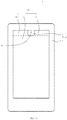
- FIG. 1 is a schematic structural diagram illustrating an electronic device according to a first implementation
- FIG. 2 is a schematic structural diagram illustrating a touch display module according to the first implementation.
- the electronic device includes, but is not limited to, a smart phone, a mobile internet device (MID), an e-book, a play station portable (PSP), a personal digital assistant (PDA), and other devices.
- MID mobile internet device
- PSP play station portable
- PDA personal digital assistant
- an electronic device 1 includes a touch display module 10.
- the touch display module 10 has a display function and a touch function.
- the touch display module 10 includes a touch display panel 100.
- the touch display panel 100 includes a first pixel area 160a and a second pixel area 160b.
- the first pixel area 160a includes a first pixel(s) 165a.
- An RC load of the first pixel 165a is a first load.
- the second pixel area 160b includes a second pixel(s) 165b.
- An RC load of the second pixel 165b is a second load.
- the first load is not equal to the second load.
- the first pixel area 160a is provided with a first electrode 111a corresponding to the first pixel 165a.
- the second pixel area 160b is provided with a second electrode 111b corresponding to the second pixel 165b.
- the first electrode 111a is spaced apart from the second electrode 111b a.
- the touch display panel 100 is operable with a display mode. When the touch display panel 100 is in the display mode, the first electrode 111a is electrically coupled with the second electrodes 111b, and the first electrode 111a and the second electrode 111b are common electrodes.
- the term "first” used in the "first pixel area 160a" of the disclosure and the term “second” used in the "second pixel area 160b" of the disclosure are for descriptive purposes only, and should not be understood as indicating or implying relative importance or the number of technical features indicated. Similarly, other descriptions of the disclosure related to "first” and “second” are for descriptive purposes only, and should not be understood as indicating or implying relative importance or the number of technical features indicated.
- the touch display panel 100 is further operable with a touch mode.
- the first electrode 111a is electrically insulated from the second electrode 111b.
- the touch display panel 100 can display an image, text, a video, and the like.
- the touch display panel 100 can accept a touch operation instruction.
- the touch display panel 100 may have uneven brightness when displaying an image, which reduces display quality of the touch display panel 100.
- the first electrode 111a which is used as the common electrode
- the second electrode 111b which is also used as the common electrode.
- a load loaded on the first pixel 165a is the same as an RC load loaded on the second pixel 165b.
- the current flowing through the first pixel 165a is the same as the current flowing through the second pixel 165b, as such, the brightness presented by the first pixel 165a is the same as the brightness presented by the second pixel 165b, thereby improving the display quality of the touch display panel 100.
- a time period for the touch display panel 100 to display the frame of the image includes a first time period and a second time period successively.
- the touch display panel 100 is in the display mode during the first time period.
- the touch display panel is in the touch mode during the second time period.
- the time period for the touch display panel 100 to display a frame of an image includes the first time period and the second time period successively.
- the first time period during which the touch display panel 100 is in the display mode does not occupy the entire time period during which the touch display panel 100 displays a frame of an image, human eyes will not perceive the time interval when the touch display panel 100 displays a frame of an image due to visual residue of the human eyes, but will perceive that screen display continues for the first time period and the second time period.
- the touch display module 10 is further in a buffer time period before the first time period.
- the buffer time period is configured to release remained power for displaying a previous frame of an image on the touch display panel 100.
- the buffer time period is set, and the buffer time period is before the first time period in which the touch display panel 100 is in the display mode.
- the touch display panel 100 releases the remained power for displaying a previous frame of an image.
- the touch display panel 100 is not affected by the remained power for displaying the previous frame of the image when displaying a current frame of an image, which improves display quality of displaying the current frame of the image, and accordingly, display quality of the touch display panel 100 can be improved.
- the touch display module 10 further includes a first switch(es) 200, a second switch(es) 300, a first transmission line 400, and a second transmission line 500.
- the first electrode 111a is electrically coupled with the second electrode 111b via the first switch 200, the second switch 300, the first transmission line 400, and the second transmission line 500.
- the first switch 200 includes a first control end 200a, a first connection end 200b, and a second connection end 200c.
- the first control end 200a is electrically coupled with the first transmission line 400.
- the first connection end 200b is electrically coupled with the first electrode 111a.
- the second connection end 200c is electrically coupled with the second transmission line 500.
- the second switch 300 includes a second control end 300a, a third connection end 300b, and a fourth connection end 300c.
- the second control end 300a is electrically coupled with the first transmission line 400.
- the third connection end 300b is electrically coupled with the second electrode 111b.
- the fourth connection end 300c is electrically coupled with the second transmission line 500.
- the first transmission line 400 is configured to be loaded with a first control signal and the second transmission line 500 is configured to be loaded with a second control signal.
- the first control signal is configured to control the first switch 200 and the second switch 300 to switch on.
- the first control signal is configured to control the first switch 200 and the second switch 300 to switch off.
- the second control signal is a common voltage signal.
- the first switch 200 and the second switch 300 are both thin film transistors, the first control end 200a and the second control end 300a are gates of the thin film transistors, the first connection end 200b and the third connection end 300b are drains of the thin film transistors, and the second connection end 200c and the fourth connection end 300c are sources of the thin film transistors.
- the first switch 200 and the second switch 300 are both thin film transistors, the first control end 200a and the second control end 300a are gates of the thin film transistors, the first connection end 200b and the third connection end 300b are sources of the thin film transistors, and the second connection end 200c and the fourth connection end 300c are drains of the thin film transistors.
- FIG. 5 is a timing diagram of a first control signal and a second control signal in a touch display panel at respective stages, when a first switch and a second switch in the touch display panel are N-type thin film transistors.
- the first control signal when the touch display panel 100 is in the display mode, the first control signal is at high level and the second control signal is at low level; when the touch display panel 100 is in the touch mode, the first control signal is at low level and the second control signal is at low level.
- the first control signal is at low level and the second control signal is at low level.
- FIG. 6 is a timing diagram of a first control signal and a second control signal in a touch display panel at respective stages, when a first switch and a second switch in the touch display panel are P-type thin film transistors.
- the first control signal when the touch display panel 100 is in the display mode, the first control signal is at low level and the second control signal is at low level; when the touch display panel 100 is in the touch mode, the first control signal is at high level and the second control signal is at low level.
- the touch display module 10 when the touch display module 10 is in the buffer time period, the first control signal is at high level and the second control signal is at low level.
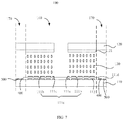
- FIG. 7 is a schematic structural diagram taken along line II-II of FIG. 1 .
- the touch display panel 100 includes a first substrate 110.
- the first substrate 110 is provided with common electrodes 111c.
- the common electrodes include a plurality of first electrodes 111a which are spaced apart from one another and a plurality of second electrodes 111b which are spaced apart from one another.
- the first substrate 110 is further provided with a pixel electrode(s) 112.
- the pixel electrode 112 is insulated from the common electrode 111c.
- an insulating layer 111d is disposed between the pixel electrode 112 and the common electrode 111c.
- the insulating layer 111d is used to insulate the pixel electrode 112 and the common electrode 111c.
- the touch display panel 100 further includes a second substrate 120 and a liquid crystal layer 130.
- the second substrate 120 is spaced apart from the first substrate 110.
- the second substrate 120 is provided with a light-filtering unit 121.
- the liquid crystal layer 130 is disposed between the first substrate 110 and the second substrate 120.
- the light-filtering unit 121 is configured to allow lights of a preset color to pass through.
- the first substrate 110 is a thin-film transistor array substrate of the touch display panel 100
- the second substrate 120 is a color film substrate of the touch display panel 100.
- the pixel electrode 112 When the touch display panel 100 is in the display mode, the pixel electrode 112 is loaded with a pixel voltage, and the common electrode is loaded with a common voltage.
- the pixel voltage and the common voltage cooperate with each other to achieve flipping of liquid crystal molecules in the liquid crystal layer 130 (i.e., flipping by a specific angle).
- the touch display panel 100 includes a display area 160 which is transparent and a non-display area 170 which is non-transparent (see FIG. 1 to FIG. 7 ).
- the first switch 200, the second switch 300, the first transmission line 400, and the second transmission line 500 are all disposed in the non-display area 170. Positions of the first switch 200, the second switch 300, the first transmission line 400, and the second transmission line 500 in the non-display area 170 are illustrated.
- the first switch 200, the second switch 300, the first transmission line 400, and the second transmission line 500 are disposed on the array substrate (i.e., the first substrate), the first transmission line 400 and the second transmission line 500 are disposed in the non-display area 170, and the first transmission line 400 and the second transmission line 500 are spaced apart from one another and disposed on the array substrate.
- FIG. 8 is a schematic structural diagram illustrating a display area and a non-display body area in the touch display module according to a first implementation.
- the touch display panel 100 further includes a display area 160 disposed adjacent to a non-display area 170.
- the display area 160 includes a display body area 161 (i.e., a main display area), a first display extension area 162, and a second display extension area 163.
- the first display extension area 162 and the second display extension area 163 are extended from a same side of the display body area 161.
- the first display extension area 162 is spaced apart from the second display extension area 163.
- the non-display area 170 includes a non-display body area 171 (i.e., a main non-display area) and a non-display extension area 172 which is extended from the non-display body area 171 towards the display area 160.
- the non-display extension area 172 is sandwiched between the first display extension area 162 and the second display extension area 163.
- the non-display extension area 172 is U-shaped.
- the first pixel area 160a is located in the display area 160 adjacent to the non-display area 170.
- the first pixel area 160a has an area smaller than the second pixel area 160b.
- FIG. 9 is a schematic structural diagram illustrating a touch display module according to a second implementation
- FIG. 10 is a cross sectional structural diagram taken along line III-III of FIG. 9
- the touch display module 10 of the second implementation is basically the same in structure as the touch display module 10 of the first implementation, except that in the second implementation, the first transmission line 400 and the second transmission line 500 are at least partially stacked and an insulating layer 600 is provided between the first transmission line 400 and the second transmission line 500.
- the first transmission line 400 and the second transmission line 500 are disposed in the non-display area 170, in this implementation, the first transmission line 400 and the second transmission line 500 are at least partially stacked, which can reduce a width of the non-display area 170, thereby facilitating realization of a narrow border.
- the insulating layer 111d and the insulating layer 600 are designed to form an integral insulating layer.
- the touch display module 10 further includes a driving chip 700 and a flexible circuit board 800.
- the driving chip 700 is configured to generate a first control signal and a second control signal.
- the driving chip 700 includes a dummy pin(s) 710 and a touch signal pin(s) 720.
- the dummy pin 710 is electrically coupled with the flexible circuit board 800 and electrically coupled with the second transmission line 500 via the flexible circuit board 800, to transmit the second control signal to the second transmission line 500.
- the touch signal pin 720 is configured to output a driving signal to the first electrodes 111a and the second electrodes 111b and transmit a detection signal detected to the driving chip 700 when the touch display module 10 is in the touch mode.
- each first electrode 111a and each second electrode 111b are independent of each other.
- the detection signal detected is used to detect whether the touch display panel 100 receives a touch operation instruction and to detect a position of the touch operation instruction.
- the touch display module 10 includes a touch display panel 100.
- the touch display panel 100 includes a first pixel area 160a and a second pixel area 160b.
- the first pixel area 160a includes a first pixel(s).
- An RC load of the first pixel 165a is a first load.
- the second pixel area 160b includes a second pixel(s) 165b.
- An RC load of the second pixel 165b is a second load.
- the first load is not equal to the second load.
- the touch display panel 100 is operable with a display mode. When the touch display module 10 is in the display mode, the first pixel area 160a and the second pixel area 160b are loaded with a same driving current, so that brightness of the first pixel area 160a is the same as that of the second pixel area 160b.
- the touch display panel 100 is further operable with a touch mode.
- the touch display panel 100 is configured to detect a touch signal on the touch display panel 100.
- a time period during which the touch display panel 100 displays a frame of an image includes a first time period and a second time period that are consecutive in sequence.
- the touch display panel 100 is in the display mode during the first time period.
- the touch display panel 100 is in the touch mode during the second time period.
- the time period during which the touch display panel 100 displays a frame of an image further includes a buffer time period before the first time period.
- the touch display panel 100 is configured to release remained power for displaying a previous frame of an image.
- FIG. 11 is a schematic structural diagram illustrating an electronic device according to a second implementation. An electronic device 1 is further provided. As illustrated in FIG. 11 , the electronic device 1 includes a touch display module 10 and a functional component 20. For details, reference may be made to the related descriptions in the foregoing touch display module 10, and it will not be described in further detail herein.
- the functional component 20 may be, but not limited to, a proximity sensor, a front camera, or the like.
- the touch display panel 100 further includes a display area 160 disposed adjacent to a non-display area 170.
- the display area 160 includes a display body area 161, a first display extension area 162, and a second display extension area 163.
- the first display extension area 162 and the second display extension area 163 are extended from a same side of the display body area 161.
- the first display extension area 162 is spaced apart from the second display extension area 163.
- the non-display area 170 includes a non-display body area 171 and a non-display extension area 172 which is extended from the non-display body area 171 towards the display area 160.
- the non-display extension area 172 is sandwiched between the first display extension area 162 and the second display extension area 163.
- the functional component 20 is disposed in the non-display extension area 172.
- the functional component 20 is disposed in the non-display extension area 172 and an area where the non-display body area 171 is connected to the non-display extension area 172.
Landscapes
- Physics & Mathematics (AREA)
- Engineering & Computer Science (AREA)
- Nonlinear Science (AREA)
- General Physics & Mathematics (AREA)
- Theoretical Computer Science (AREA)
- General Engineering & Computer Science (AREA)
- Crystallography & Structural Chemistry (AREA)
- Chemical & Material Sciences (AREA)
- Optics & Photonics (AREA)
- Mathematical Physics (AREA)
- Human Computer Interaction (AREA)
- Geometry (AREA)
- Computer Hardware Design (AREA)
- Quality & Reliability (AREA)
- Liquid Crystal (AREA)
- Devices For Indicating Variable Information By Combining Individual Elements (AREA)
- Position Input By Displaying (AREA)
Abstract
Description
- This application claims priority to Chinese Patent Application No.
201810597852.1, filed on June 11, 2018 201820900747.6, filed on June 11, 2018 - This disclosure relates to the field of electronic equipment, and particularly to a touch display module and an electronic device.
- An electronic device such as a mobile phone usually includes a backlight module and a display screen. The backlight module is generally used to provide light for the display screen. The display screen usually includes a common electrode and a pixel electrode. The common electrode and the pixel electrode cooperate with each other to achieve flipping of liquid crystal molecules in the display screen. After lights emitted from the backlight module enter into the display screen, there will be different transmittances due to different flip angles of the liquid crystal molecules. When there is more light passing through a pixel area of the display screen, brightness of the pixel area is relatively bright. When there is few light passing through a pixel area of the display screen, the brightness of the pixel area is relatively dark. In this way, the display screen presents an image. However, if the display screen is integrated with a touch function, if both a display function and the touch function are taken into consideration, brightness of the display screen may be uneven due to various reasons when the display screen displays an image, which resulting in reduced display quality in display of the display screen.
- According to the disclosure, a touch display module is provided. The touch display module includes a touch display panel. The touch display panel is provided with a first pixel area and a second pixel area. The first pixel area includes a first pixel. A resistor-capacitance (RC) load of the first pixel is a first load. The second pixel area includes a second pixel. An RC load of the second pixel is a second load, and the first load is not equal to the second load. The first pixel area is provided with a first electrode corresponding to the first pixel. The second pixel area is provided with a second electrode corresponding to the second pixel. The first electrode is spaced apart from the second electrode. The touch display panel is operable with a display mode. When the touch display panel is in the display mode, the first electrode is electrically coupled with the second electrode, and the first electrode and the second electrode are common electrodes.
- According to the disclosure, a touch display module is provided. The touch display module includes a touch display panel. The touch display panel is provided with a first pixel area and a second pixel area. The first pixel area includes a first pixel. An RC load of the first pixel is a first load. The second pixel area includes a second pixel. An RC load of the second pixel is a second load. The first load is not equal to the second load. The touch display panel is operable with a display mode. When the touch display module is in the display mode, the first pixel area and the second pixel area are loaded with a same driving voltage, so that brightness of the first pixel area is the same as that of the second pixel area.
- According to the disclosure, an electronic device is provided. The electronic device includes the foregoing touch display module.
- In order to describe technical solutions of implementations of the disclosure more clearly, the following will give a brief description of accompanying drawings used for describing the implementations. Apparently, accompanying drawings described below are merely some implementations. Those of ordinary skill in the art can also obtain other accompanying drawings based on the accompanying drawings described below without creative efforts.
-
FIG. 1 is a schematic structural diagram illustrating an electronic device according to a first implementation. -
FIG. 2 is a schematic structural diagram illustrating a touch display module according to a first implementation. -
FIG. 3 is an enlarged schematic diagram at I ofFIG. 2 according to some implementations. -
FIG. 4 is an enlarged schematic diagram at I ofFIG. 2 according to other implementations. -
FIG. 5 is a timing diagram of a first control signal and a second control signal in a touch display panel at respective stages, when a first switch and a second switch in the touch display panel are N-type thin film transistors. -
FIG. 6 is a timing diagram of a first control signal and a second control signal in a touch display panel at respective stages, when a first switch and a second switch in the touch display panel are P-type thin film transistors. -
FIG. 7 is a schematic structural diagram taken along line II-II ofFIG. 1 . -
FIG. 8 is a schematic structural diagram illustrating a display area and a non-display body area in the touch display module according to a first implementation. -
FIG. 9 is a schematic structural diagram illustrating a touch display module according to a second implementation. -
FIG. 10 is a cross sectional structural diagram taken along line III-III ofFIG. 9 . -
FIG. 11 is a schematic structural diagram illustrating an electronic device according to a second implementation. - In a first aspect of the disclosure, a touch display module is provided. The touch display module includes a touch display panel. The touch display panel is provided with a first pixel area and a second pixel area. The first pixel area includes a first pixel. A resistor-capacitance (RC) load of the first pixel is a first load. The second pixel area includes a second pixel. An RC load of the second pixel is a second load. The first load is not equal to the second load. The first pixel area is provided with a first electrode corresponding to the first pixel. The second pixel area is provided with a second electrode corresponding to the second pixel. The first electrode is spaced apart from the second electrode. The touch display panel is operable with a display mode. When the touch display panel is in the display mode, the first electrode is electrically coupled with the second electrode. The first electrode and the second electrode are common electrodes.
- In a first implementation according to the first aspect, the touch display panel is further operable with a touch mode. When the touch display panel is in the touch mode, the first electrode is electrically insulated from the second electrode.
- In a second implementation according to the first implementation, the touch display module further includes a first switch, a second switch, a first transmission line, and a second transmission line. When the touch display panel is in the display mode, the first electrode is electrically coupled with the second electrode via the first switch, the second switch, the first transmission line, and the second transmission line.
- In a third implementation according to the second implementation, the first switch includes a first control end, a first connection end, and a second connection end. The first control end is electrically coupled with the first transmission line. The first connection end is electrically coupled with the first electrode. The second connection end is electrically coupled with the second transmission line. The second switch includes a second control end, a third connection end, and a fourth connection end. The second control end is electrically coupled with the first transmission line. The third connection end is electrically coupled with the second electrode. The fourth connection end is electrically coupled with the second transmission line. The first transmission line is configured to be loaded with a first control signal. The second transmission line is configured to be loaded with a second control signal. The first control signal is suitable for controlling the first switch and the second switch to switch on when the touch display panel is in the display mode, where the second control signal is a common voltage signal.
- In a fourth implementation according to the third implementation, when the touch display panel is in the touch mode, the first control signal is suitable for controlling the first switch and the second switch to switch off.
- In a fifth implementation, the touch display panel includes a first substrate. The first substrate is provided with common electrodes. The common electrodes include a plurality of first electrodes spaced apart from one another and a plurality of second electrodes spaced apart from one another.
- In a sixth implementation according to the fifth implementation, the first substrate is further provided with pixel electrodes. The pixel electrodes are insulated from the common electrodes.
- In a seventh implementation according to the sixth implementation, the touch display panel further includes a second substrate and a liquid crystal layer. The second substrate is spaced apart from the first substrate. The second substrate is provided with a light-filtering unit. The liquid crystal layer is disposed between the first substrate and the second substrate.
- In an eighth implementation according to the second implementation, the touch display panel includes a non-display area which is non-transparent. The first switch, the second switch, the first transmission line, and the second transmission line are all disposed in the non-display area.
- In a ninth implementation according to the eighth implementation, the first transmission line and the second transmission line are at least partially stacked. An insulating layer is provided between the first transmission line and the second transmission line.
- In a tenth implementation according to the eighth implementation, the touch display panel further includes a display area. The display area is disposed adjacent to the non-display area and includes a display body area, a first display extension area, and a second display extension area. The first display extension area and the second display extension area are extended from a same side of the display body area. The first display extension area is spaced apart from the second display extension area. The non-display area includes a non-display body area and a non-display extension area which is extended from the non-display body area towards the display area. The non-display extension area is sandwiched between the first display extension area and the second display extension area.
- In an eleventh implementation according to the tenth implementation, the first pixel area is located in the display area adjacent to the non-display area. An area of the first pixel area is smaller than an area of the second pixel area.
- In a twelfth implementation according to the first implementation, a time period for the touch display panel to display a frame of an image includes a first time period and a second time period successively. The touch display panel is in the display mode during the first time period. The touch display panel is in the touch mode during the second time period.
- In a thirteenth implementation according to the twelfth implementation, the time period for the touch display panel to display a frame of an image further includes a buffer time period before the first time period. When the display panel is in the buffer time period, the touch display panel is configured to release remained power for displaying a previous frame of an image.
- In a fourteenth implementation according to the third implementation or the fourth implementation, the touch display module further includes a driving chip and a flexible circuit board. The driving chip is configured to generate the second control signal. The driving chip includes a dummy pin. The dummy pin is electrically coupled with the flexible circuit board and electrically coupled with the second transmission line via the flexible circuit board to transmit the second control signal to the second transmission line.
- In a second aspect of the disclosure, a touch display module is provided. The touch display module includes a touch display panel. The touch display panel is provided with a first pixel area and a second pixel area. The first pixel area includes a first pixel. An RC load of the first pixel is a first load. The second pixel area includes a second pixel. An RC load of the second pixel is a second load. The first load is not equal to the second load. The touch display panel is operable with a display mode. When the touch display module is in the display mode, the first pixel area and the second pixel area are loaded with a same driving voltage, so that brightness of the first pixel area is the same as that of the second pixel area.
- In a first implementation, the touch display panel is further operable with a touch mode. When the touch display panel is in the touch mode, the touch display panel is configured to detect a touch signal of the touch display panel. A time period for the touch display panel to display a frame of an image includes a first time period and a second time period successively. The touch display panel is in the display mode during the first time period. The touch display panel is in the touch mode during the second time period.
- In a second implementation according to the first implementation, the time period for the touch display panel to display a frame of an image further includes a buffer time period before the first time period. When the touch display panel is in the buffer time period, the touch display panel is configured to release remained power for displaying a previous frame of an image.
- In a second implementation according to the first implementation, the first pixel area is provided with a first electrode corresponding to the first pixel. The second pixel area is provided with a second electrode corresponding to the second pixel. The first electrode is spaced apart from the second electrode. When the touch display panel is in the touch mode, the first electrode is electrically insulated from the second electrode.
- In a third aspect of the disclosure, an electronic device is provided. The electronic device includes the touch display module according to the first aspect, any of the implementations of the first aspect, the second aspect, and any of the implementations of the second aspect.
- Hereinafter, technical solutions embodied by the implementations of the disclosure will be described in a clear and comprehensive manner with reference to the accompanying drawings intended for the implementations. It is evident that the implementations described herein constitute merely some rather than all of the implementations of the disclosure, and that those of ordinary skill in the art will be able to derive other implementations based on these implementations without making creative efforts, which all such derived implementations shall all fall in the protection scope of the disclosure.
- Referring to
FIG. 1 andFIG. 2 ,FIG. 1 is a schematic structural diagram illustrating an electronic device according to a first implementation, andFIG. 2 is a schematic structural diagram illustrating a touch display module according to the first implementation. The electronic device includes, but is not limited to, a smart phone, a mobile internet device (MID), an e-book, a play station portable (PSP), a personal digital assistant (PDA), and other devices. - As illustrated in
FIG. 1 andFIG. 2 , anelectronic device 1 includes atouch display module 10. Thetouch display module 10 has a display function and a touch function. Thetouch display module 10 includes atouch display panel 100. Thetouch display panel 100 includes afirst pixel area 160a and asecond pixel area 160b. Thefirst pixel area 160a includes a first pixel(s) 165a. An RC load of thefirst pixel 165a is a first load. Thesecond pixel area 160b includes a second pixel(s) 165b. An RC load of thesecond pixel 165b is a second load. The first load is not equal to the second load. Thefirst pixel area 160a is provided with afirst electrode 111a corresponding to thefirst pixel 165a. Thesecond pixel area 160b is provided with asecond electrode 111b corresponding to thesecond pixel 165b. Thefirst electrode 111a is spaced apart from thesecond electrode 111b a. Thetouch display panel 100 is operable with a display mode. When thetouch display panel 100 is in the display mode, thefirst electrode 111a is electrically coupled with thesecond electrodes 111b, and thefirst electrode 111a and thesecond electrode 111b are common electrodes. The term "first" used in the "first pixel area 160a" of the disclosure and the term "second" used in the "second pixel area 160b" of the disclosure are for descriptive purposes only, and should not be understood as indicating or implying relative importance or the number of technical features indicated. Similarly, other descriptions of the disclosure related to "first" and "second" are for descriptive purposes only, and should not be understood as indicating or implying relative importance or the number of technical features indicated. - Further, the
touch display panel 100 is further operable with a touch mode. When thetouch display panel 100 is in the touch mode, thefirst electrode 111a is electrically insulated from thesecond electrode 111b. When thetouch display panel 100 is in the display mode, thetouch display panel 100 can display an image, text, a video, and the like. When thetouch display panel 100 is in the touch mode, thetouch display panel 100 can accept a touch operation instruction. - If the
first electrode 111a is electrically insulated from thesecond electrode 111b, since a load value of a first load of thefirst pixel 165a is different from that of a second load of thesecond pixel 165b, a current flowing through thefirst pixel 165a is different from a current flowing through thesecond pixel 165b when a voltage applied to thefirst electrode 111a is the same as a voltage applied to thesecond electrode 111b, as such, brightness presented by thefirst pixel 165a is different from brightness presented by thesecond pixel 165b. That is, thetouch display panel 100 may have uneven brightness when displaying an image, which reduces display quality of thetouch display panel 100. According to the disclosure, when thetouch display module 10 is in the display mode, thefirst electrode 111a, which is used as the common electrode, is electrically coupled with thesecond electrode 111b, which is also used as the common electrode. In this case, a load loaded on thefirst pixel 165a is the same as an RC load loaded on thesecond pixel 165b. When a voltage applied to thefirst pixel 165a is the same as a voltage applied to thesecond pixel 165b, the current flowing through thefirst pixel 165a is the same as the current flowing through thesecond pixel 165b, as such, the brightness presented by thefirst pixel 165a is the same as the brightness presented by thesecond pixel 165b, thereby improving the display quality of thetouch display panel 100. - Referring to
FIG. 5 or FIG. 6 , when thetouch display panel 100 displays a frame of an image, a time period for thetouch display panel 100 to display the frame of the image includes a first time period and a second time period successively. Thetouch display panel 100 is in the display mode during the first time period. The touch display panel is in the touch mode during the second time period. According to the disclosure, the time period for thetouch display panel 100 to display a frame of an image includes the first time period and the second time period successively. Although the first time period during which thetouch display panel 100 is in the display mode does not occupy the entire time period during which thetouch display panel 100 displays a frame of an image, human eyes will not perceive the time interval when thetouch display panel 100 displays a frame of an image due to visual residue of the human eyes, but will perceive that screen display continues for the first time period and the second time period. - Further, when the
touch display panel 100 displays a frame of an image, thetouch display module 10 is further in a buffer time period before the first time period. The buffer time period is configured to release remained power for displaying a previous frame of an image on thetouch display panel 100. According to the disclosure, the buffer time period is set, and the buffer time period is before the first time period in which thetouch display panel 100 is in the display mode. When thetouch display panel 100 is in the buffer time period, thetouch display panel 100 releases the remained power for displaying a previous frame of an image. In this way, thetouch display panel 100 is not affected by the remained power for displaying the previous frame of the image when displaying a current frame of an image, which improves display quality of displaying the current frame of the image, and accordingly, display quality of thetouch display panel 100 can be improved. - Further, the
touch display module 10 further includes a first switch(es) 200, a second switch(es) 300, afirst transmission line 400, and asecond transmission line 500. When thetouch display panel 100 is in the display mode, thefirst electrode 111a is electrically coupled with thesecond electrode 111b via thefirst switch 200, thesecond switch 300, thefirst transmission line 400, and thesecond transmission line 500. - Referring to
FIG. 3 or FIG. 4, FIG. 3 is an enlarged schematic diagram at I ofFIG. 2 according to some implementations, andFIG. 4 is an enlarged schematic diagram at I ofFIG. 2 according to other implementations. In one implementation, thefirst switch 200 includes afirst control end 200a, afirst connection end 200b, and asecond connection end 200c. Thefirst control end 200a is electrically coupled with thefirst transmission line 400. Thefirst connection end 200b is electrically coupled with thefirst electrode 111a. Thesecond connection end 200c is electrically coupled with thesecond transmission line 500. In one implementation, thesecond switch 300 includes asecond control end 300a, a third connection end 300b, and a fourth connection end 300c. Thesecond control end 300a is electrically coupled with thefirst transmission line 400. The third connection end 300b is electrically coupled with thesecond electrode 111b. The fourth connection end 300c is electrically coupled with thesecond transmission line 500. Thefirst transmission line 400 is configured to be loaded with a first control signal and thesecond transmission line 500 is configured to be loaded with a second control signal. When thetouch display panel 100 is in the display mode, the first control signal is configured to control thefirst switch 200 and thesecond switch 300 to switch on. When thetouch display panel 100 is in the touch mode, the first control signal is configured to control thefirst switch 200 and thesecond switch 300 to switch off. The second control signal is a common voltage signal. - In one implementation, the
first switch 200 and thesecond switch 300 are both thin film transistors, thefirst control end 200a and thesecond control end 300a are gates of the thin film transistors, thefirst connection end 200b and the third connection end 300b are drains of the thin film transistors, and thesecond connection end 200c and the fourth connection end 300c are sources of the thin film transistors. Alternatively, in another implementation, thefirst switch 200 and thesecond switch 300 are both thin film transistors, thefirst control end 200a and thesecond control end 300a are gates of the thin film transistors, thefirst connection end 200b and the third connection end 300b are sources of the thin film transistors, and thesecond connection end 200c and the fourth connection end 300c are drains of the thin film transistors. - In one implementation described in conjunction with
FIG. 3 , thefirst switch 200 and thesecond switch 300 are N-type thin film transistors.FIG. 5 is a timing diagram of a first control signal and a second control signal in a touch display panel at respective stages, when a first switch and a second switch in the touch display panel are N-type thin film transistors. As illustrated inFIG. 5 , when thetouch display panel 100 is in the display mode, the first control signal is at high level and the second control signal is at low level; when thetouch display panel 100 is in the touch mode, the first control signal is at low level and the second control signal is at low level. In this implementation, when thetouch display module 10 is in the buffer time period, the first control signal is at low level and the second control signal is at low level. - In one implementation described in conjunction with
FIG. 4 , thefirst switch 200 and thesecond switch 300 are P-type thin film transistors.FIG. 6 is a timing diagram of a first control signal and a second control signal in a touch display panel at respective stages, when a first switch and a second switch in the touch display panel are P-type thin film transistors. As illustrated inFIG. 6 , when thetouch display panel 100 is in the display mode, the first control signal is at low level and the second control signal is at low level; when thetouch display panel 100 is in the touch mode, the first control signal is at high level and the second control signal is at low level. In this implementation, when thetouch display module 10 is in the buffer time period, the first control signal is at high level and the second control signal is at low level. -
FIG. 7 is a schematic structural diagram taken along line II-II ofFIG. 1 . In one implementation, as illustrated inFIG. 7 , thetouch display panel 100 includes afirst substrate 110. Thefirst substrate 110 is provided withcommon electrodes 111c. The common electrodes include a plurality offirst electrodes 111a which are spaced apart from one another and a plurality ofsecond electrodes 111b which are spaced apart from one another. Thefirst substrate 110 is further provided with a pixel electrode(s) 112. Thepixel electrode 112 is insulated from thecommon electrode 111c. As illustrated inFIG. 7 , an insulatinglayer 111d is disposed between thepixel electrode 112 and thecommon electrode 111c. The insulatinglayer 111d is used to insulate thepixel electrode 112 and thecommon electrode 111c. Thetouch display panel 100 further includes asecond substrate 120 and aliquid crystal layer 130. Thesecond substrate 120 is spaced apart from thefirst substrate 110. Thesecond substrate 120 is provided with a light-filtering unit 121. Theliquid crystal layer 130 is disposed between thefirst substrate 110 and thesecond substrate 120. The light-filtering unit 121 is configured to allow lights of a preset color to pass through. Thefirst substrate 110 is a thin-film transistor array substrate of thetouch display panel 100, and thesecond substrate 120 is a color film substrate of thetouch display panel 100. When thetouch display panel 100 is in the display mode, thepixel electrode 112 is loaded with a pixel voltage, and the common electrode is loaded with a common voltage. The pixel voltage and the common voltage cooperate with each other to achieve flipping of liquid crystal molecules in the liquid crystal layer 130 (i.e., flipping by a specific angle). - In this implementation, the
touch display panel 100 includes adisplay area 160 which is transparent and anon-display area 170 which is non-transparent (seeFIG. 1 to FIG. 7 ). Thefirst switch 200, thesecond switch 300, thefirst transmission line 400, and thesecond transmission line 500 are all disposed in thenon-display area 170. Positions of thefirst switch 200, thesecond switch 300, thefirst transmission line 400, and thesecond transmission line 500 in thenon-display area 170 are illustrated. In one implementation, thefirst switch 200, thesecond switch 300, thefirst transmission line 400, and thesecond transmission line 500 are disposed on the array substrate (i.e., the first substrate), thefirst transmission line 400 and thesecond transmission line 500 are disposed in thenon-display area 170, and thefirst transmission line 400 and thesecond transmission line 500 are spaced apart from one another and disposed on the array substrate. -
FIG. 8 is a schematic structural diagram illustrating a display area and a non-display body area in the touch display module according to a first implementation. As illustrated inFIG. 8 , thetouch display panel 100 further includes adisplay area 160 disposed adjacent to anon-display area 170. Thedisplay area 160 includes a display body area 161 (i.e., a main display area), a firstdisplay extension area 162, and a seconddisplay extension area 163. The firstdisplay extension area 162 and the seconddisplay extension area 163 are extended from a same side of thedisplay body area 161. The firstdisplay extension area 162 is spaced apart from the seconddisplay extension area 163. Thenon-display area 170 includes a non-display body area 171 (i.e., a main non-display area) and anon-display extension area 172 which is extended from thenon-display body area 171 towards thedisplay area 160. Thenon-display extension area 172 is sandwiched between the firstdisplay extension area 162 and the seconddisplay extension area 163. In this implementation, thenon-display extension area 172 is U-shaped. - The
first pixel area 160a is located in thedisplay area 160 adjacent to thenon-display area 170. Thefirst pixel area 160a has an area smaller than thesecond pixel area 160b. - Referring to
FIG. 9 andFIG. 10 ,FIG. 9 is a schematic structural diagram illustrating a touch display module according to a second implementation, andFIG. 10 is a cross sectional structural diagram taken along line III-III ofFIG. 9 . Thetouch display module 10 of the second implementation is basically the same in structure as thetouch display module 10 of the first implementation, except that in the second implementation, thefirst transmission line 400 and thesecond transmission line 500 are at least partially stacked and an insulating layer 600 is provided between thefirst transmission line 400 and thesecond transmission line 500. Since thefirst transmission line 400 and thesecond transmission line 500 are disposed in thenon-display area 170, in this implementation, thefirst transmission line 400 and thesecond transmission line 500 are at least partially stacked, which can reduce a width of thenon-display area 170, thereby facilitating realization of a narrow border. In this implementation, the insulatinglayer 111d and the insulating layer 600 are designed to form an integral insulating layer. - Referring to
FIG. 2 andFIG. 9 , thetouch display module 10 further includes adriving chip 700 and aflexible circuit board 800. Thedriving chip 700 is configured to generate a first control signal and a second control signal. Thedriving chip 700 includes a dummy pin(s) 710 and a touch signal pin(s) 720. Thedummy pin 710 is electrically coupled with theflexible circuit board 800 and electrically coupled with thesecond transmission line 500 via theflexible circuit board 800, to transmit the second control signal to thesecond transmission line 500. Thetouch signal pin 720 is configured to output a driving signal to thefirst electrodes 111a and thesecond electrodes 111b and transmit a detection signal detected to thedriving chip 700 when thetouch display module 10 is in the touch mode. When thetouch display module 710 is in the touch display mode, eachfirst electrode 111a and eachsecond electrode 111b are independent of each other. The detection signal detected is used to detect whether thetouch display panel 100 receives a touch operation instruction and to detect a position of the touch operation instruction. - With reference to the foregoing
touch display module 10, anothertouch display module 10 is further provided. Thetouch display module 10 includes atouch display panel 100. Thetouch display panel 100 includes afirst pixel area 160a and asecond pixel area 160b. Thefirst pixel area 160a includes a first pixel(s). An RC load of thefirst pixel 165a is a first load. Thesecond pixel area 160b includes a second pixel(s) 165b. An RC load of thesecond pixel 165b is a second load. The first load is not equal to the second load. Thetouch display panel 100 is operable with a display mode. When thetouch display module 10 is in the display mode, thefirst pixel area 160a and thesecond pixel area 160b are loaded with a same driving current, so that brightness of thefirst pixel area 160a is the same as that of thesecond pixel area 160b. - The
touch display panel 100 is further operable with a touch mode. When thetouch display panel 100 is in the touch mode, thetouch display panel 100 is configured to detect a touch signal on thetouch display panel 100. A time period during which thetouch display panel 100 displays a frame of an image includes a first time period and a second time period that are consecutive in sequence. Thetouch display panel 100 is in the display mode during the first time period. Thetouch display panel 100 is in the touch mode during the second time period. - The time period during which the
touch display panel 100 displays a frame of an image further includes a buffer time period before the first time period. When thetouch display panel 100 is in the buffer time period, thetouch display panel 100 is configured to release remained power for displaying a previous frame of an image. - Hereinafter, an
electronic device 1 of the disclosure will be described with reference to the foregoingtouch display module 10.FIG. 11 is a schematic structural diagram illustrating an electronic device according to a second implementation. Anelectronic device 1 is further provided. As illustrated inFIG. 11 , theelectronic device 1 includes atouch display module 10 and afunctional component 20. For details, reference may be made to the related descriptions in the foregoingtouch display module 10, and it will not be described in further detail herein. Thefunctional component 20 may be, but not limited to, a proximity sensor, a front camera, or the like. Thetouch display panel 100 further includes adisplay area 160 disposed adjacent to anon-display area 170. Thedisplay area 160 includes adisplay body area 161, a firstdisplay extension area 162, and a seconddisplay extension area 163. The firstdisplay extension area 162 and the seconddisplay extension area 163 are extended from a same side of thedisplay body area 161. The firstdisplay extension area 162 is spaced apart from the seconddisplay extension area 163. Thenon-display area 170 includes anon-display body area 171 and anon-display extension area 172 which is extended from thenon-display body area 171 towards thedisplay area 160. Thenon-display extension area 172 is sandwiched between the firstdisplay extension area 162 and the seconddisplay extension area 163. In one implementation, thefunctional component 20 is disposed in thenon-display extension area 172. In another implementation, thefunctional component 20 is disposed in thenon-display extension area 172 and an area where thenon-display body area 171 is connected to thenon-display extension area 172. - While the implementations of the disclosure have been described, it will be understood by those skilled in the art that various improvements and variants may be made without departing from the principles of the implementations of the disclosure. These improvements and variants shall all be encompassed within the protection of the disclosure.
Claims (20)
- A touch display module comprising a touch display panel, wherein
the touch display panel is provided with a first pixel area and a second pixel area; the first pixel area comprises a first pixel, a resistor-capacitance, RC, load of the first pixel is a first load, the second pixel area comprises a second pixel, an RC load of the second pixel is a second load, and the first load is not equal to the second load; the first pixel area is provided with a first electrode corresponding to the first pixel, the second pixel area is provided with a second electrode corresponding to the second pixel, and the first electrode is spaced apart from the second electrode; the touch display panel is operable with a display mode, the first electrode is electrically coupled with the second electrode when the touch display panel is in the display mode, and the first electrode and the second electrode are common electrodes. - The touch display module of claim 1, wherein the touch display panel is further operable with a touch mode, the first electrode is electrically insulated from the second electrode when the touch display panel is in the touch mode.
- The touch display module of claim 2, wherein the touch display module further comprises a first switch, a second switch, a first transmission line, and a second transmission line, the first electrode is electrically coupled with the second electrode via the first switch, the second switch, the first transmission line, and the second transmission line when the touch display panel is in the display mode.
- The touch display module of claim 3, wherein the first switch comprises a first control end, a first connection end, and a second connection end, the first control end is electrically coupled with the first transmission line, the first connection end is electrically coupled with the first electrode, and the second connection end is electrically coupled with the second transmission line; the second switch comprises a second control end, a third connection end, and a fourth connection end, the second control end is electrically coupled with the first transmission line, the third connection end is electrically coupled with the second electrode, and the fourth connection end is electrically coupled with the second transmission line; the first transmission line is configured to be loaded with a first control signal, the second transmission line is configured to be loaded with a second control signal, and the first control signal is suitable for controlling the first switch and the second switch to switch on when the touch display panel is in the display mode, wherein the second control signal is a common voltage signal.
- The touch display module of claim 4, wherein the first control signal is suitable for controlling the first switch and the second switch to switch off when the touch display panel is in the touch mode.
- The touch display module of claim 1, wherein the touch display panel comprises a first substrate, and the first substrate is provided with common electrodes, the common electrodes comprise a plurality of first electrodes spaced apart from one another and a plurality of second electrodes spaced apart from one another.
- The touch display module of claim 6, wherein the first substrate is further provided with pixel electrodes, and the pixel electrodes are insulated from the common electrodes.
- The touch display module of claim 7, wherein the touch display panel further comprises a second substrate and a liquid crystal layer, the second substrate is spaced apart from the first substrate, the second substrate is provided with a light-filtering unit, and the liquid crystal layer is disposed between the first substrate and the second substrate.
- The touch display module of claim 3, wherein the touch display panel comprises a non-display area which is non-transparent, and the first switch, the second switch, the first transmission line, and the second transmission line are all disposed in the non-display area.
- The touch display module of claim 9, wherein the first transmission line and the second transmission line are at least partially stacked, and an insulating layer is provided between the first transmission line and the second transmission line.
- The touch display module of claim 9, wherein the touch display panel further comprises a display area, the display are is disposed adjacent to the non-display area and comprises a display body area, a first display extension area, and a second display extension area, the first display extension area and the second display extension area are extended from a same side of the display body area, and the first display extension area is spaced apart from the second display extension area; the non-display area comprises a non-display body area and a non-display extension area which is extended from the non-display body area towards the display area, and the non-display extension area is sandwiched between the first display extension area and the second display extension area.
- The touch display module of claim 11, wherein the first pixel area is located in the display area adjacent to the non-display area, and an area of the first pixel area is smaller than an area of the second pixel area.
- The touch display module of claim 2, wherein a time period for the touch display panel to display a frame of an image comprises a first time period and a second time period successively, the touch display panel is in the display mode during the first time period, and the touch display panel is in the touch mode during the second time period.
- The touch display module of claim 13, wherein the time period for the touch display panel to display a frame of an image further comprises a buffer time period before the first time period, and when the display panel is in the buffer time period, the touch display panel is configured to release remained power for displaying a previous frame of an image.
- The touch display module of claim 4 or 5, wherein the touch display module further comprises a driving chip and a flexible circuit board, the driving chip is configured to generate the second control signal, the driving chip comprises a dummy pin, the dummy pin is electrically coupled with the flexible circuit board and electrically coupled with the second transmission line via the flexible circuit board to transmit the second control signal to the second transmission line.
- A touch display module comprising a touch display panel, wherein
the touch display panel is provided with a first pixel area and a second pixel area; the first pixel area comprises a first pixel, a resistor-capacitance, RC, load of the first pixel is a first load, the second pixel area comprises a second pixel, an RC load of the second pixel is a second load, and the first load is not equal to the second load; the touch display panel is operable with a display mode, the first pixel area and the second pixel area are loaded with a same driving voltage when the touch display module is in the display mode, so that brightness of the first pixel area is the same as that of the second pixel area. - The touch display module of claim 16, wherein the touch display panel is further operable with a touch mode, the touch display panel is configured to detect a touch signal of the touch display panel when the touch display panel is in the touch mode; a time period for the touch display panel to display a frame of an image comprises a first time period and a second time period successively, the touch display panel is in the display mode during the first time period, and the touch display panel is in the touch mode during the second time period.
- The touch display module of claim 17, wherein the time period for the touch display panel to display a frame of an image further comprises a buffer time period before the first time period, and when the touch display panel is in the buffer time period, the touch display panel is configured to release remained power for displaying a previous frame of an image.
- The touch display module of claim 17, wherein the first pixel area is provided with a first electrode corresponding to the first pixel, the second pixel area is provided with a second electrode corresponding to the second pixel, the first electrode is spaced apart from the second electrode, and the first electrode is electrically insulated from the second electrode when the touch display panel is in the touch mode.
- An electronic device, comprising the touch display module according to any of claims 1 to 19.
Applications Claiming Priority (3)
| Application Number | Priority Date | Filing Date | Title |
|---|---|---|---|
| CN201810597852.1A CN108535923B (en) | 2018-06-11 | 2018-06-11 | Touch display module and electronic device |
| CN201820900747.6U CN208488630U (en) | 2018-06-11 | 2018-06-11 | Touch-control display module and electronic device |
| PCT/CN2019/089377 WO2019237943A1 (en) | 2018-06-11 | 2019-05-30 | Touch control display module and electronic apparatus |
Publications (3)
| Publication Number | Publication Date |
|---|---|
| EP3751337A1 true EP3751337A1 (en) | 2020-12-16 |
| EP3751337A4 EP3751337A4 (en) | 2021-05-05 |
| EP3751337B1 EP3751337B1 (en) | 2024-04-24 |
Family
ID=68842816
Family Applications (1)
| Application Number | Title | Priority Date | Filing Date |
|---|---|---|---|
| EP19819652.9A Active EP3751337B1 (en) | 2018-06-11 | 2019-05-30 | Touch control display module and electronic apparatus |
Country Status (3)
| Country | Link |
|---|---|
| US (1) | US11199925B2 (en) |
| EP (1) | EP3751337B1 (en) |
| WO (1) | WO2019237943A1 (en) |
Families Citing this family (3)
| Publication number | Priority date | Publication date | Assignee | Title |
|---|---|---|---|---|
| US12563071B1 (en) | 2017-11-27 | 2026-02-24 | Fortinet, Inc. | Using generative artificial intelligence to interface with a knowledge graph |
| US12495052B1 (en) | 2017-11-27 | 2025-12-09 | Fortinet, Inc. | Detecting package execution for threat assessments |
| CN114974057B (en) * | 2021-02-26 | 2025-05-16 | 合肥维信诺科技有限公司 | Display panel and brightness adjustment method thereof, and display device |
Family Cites Families (14)
| Publication number | Priority date | Publication date | Assignee | Title |
|---|---|---|---|---|
| KR20140139261A (en) * | 2013-05-27 | 2014-12-05 | 삼성디스플레이 주식회사 | Display device including touch sensor and driving method thereof |
| KR102047227B1 (en) * | 2013-06-24 | 2019-11-21 | 엘지디스플레이 주식회사 | Color Filter Substrate for Display Device with Integrated Touch Screen and Method for Fabricating The Same |
| CN103761014B (en) * | 2013-11-20 | 2018-05-01 | 京东方科技集团股份有限公司 | Touch-screen and its driving method and display device |
| US10354578B2 (en) * | 2016-04-15 | 2019-07-16 | Samsung Display Co., Ltd. | Display device |
| CN209044540U (en) | 2016-09-30 | 2019-06-28 | 深圳深微创芯科技有限公司 | Touch display device and electronic apparatus |
| CN107357096B (en) * | 2017-07-31 | 2020-01-21 | 厦门天马微电子有限公司 | Special-shaped touch display panel and display device |
| CN207115380U (en) | 2017-08-26 | 2018-03-16 | 深圳欧菲光科技股份有限公司 | Contact panel and display device |
| CN107704121A (en) * | 2017-08-31 | 2018-02-16 | 京东方科技集团股份有限公司 | Touch display substrate, display device and its control method |
| US10360862B2 (en) * | 2017-09-07 | 2019-07-23 | Apple Inc. | Displays with supplemental loading structures |
| CN107481669A (en) * | 2017-09-08 | 2017-12-15 | 武汉天马微电子有限公司 | A display panel and a display device |
| CN107797705B (en) * | 2017-11-01 | 2019-09-20 | Oppo广东移动通信有限公司 | Terminal, touch electrode assembly, touch electrode plate and touch electrode plate setting method |
| CN107831937B (en) * | 2017-11-07 | 2020-11-20 | 武汉天马微电子有限公司 | A touch sensor and display device |
| CN208488630U (en) * | 2018-06-11 | 2019-02-12 | Oppo广东移动通信有限公司 | Touch-control display module and electronic device |
| CN108535923B (en) * | 2018-06-11 | 2023-11-07 | Oppo广东移动通信有限公司 | Touch display module and electronic device |
-
2019
- 2019-05-30 EP EP19819652.9A patent/EP3751337B1/en active Active
- 2019-05-30 WO PCT/CN2019/089377 patent/WO2019237943A1/en not_active Ceased
-
2020
- 2020-10-19 US US17/074,196 patent/US11199925B2/en active Active
Also Published As
| Publication number | Publication date |
|---|---|
| US11199925B2 (en) | 2021-12-14 |
| EP3751337B1 (en) | 2024-04-24 |
| EP3751337A4 (en) | 2021-05-05 |
| US20210034191A1 (en) | 2021-02-04 |
| WO2019237943A1 (en) | 2019-12-19 |
Similar Documents
| Publication | Publication Date | Title |
|---|---|---|
| US8107032B2 (en) | Active matrix substrate and display device having the same | |
| JP6424824B2 (en) | Display device and electronic device | |
| CN112908238A (en) | Display panel and electronic equipment | |
| US11199925B2 (en) | Touch display module and electronic device | |
| US8928703B2 (en) | Pixel structure | |
| US20120050659A1 (en) | Display device and electronic apparatus | |
| KR20170024182A (en) | Display device and display panel | |
| KR20110001887A (en) | LCD and its driving method | |
| US11488512B2 (en) | Display panel, display device and display control method thereof | |
| KR20060064106A (en) | LCD and mobile terminal using same | |
| CN108535923B (en) | Touch display module and electronic device | |
| WO2020259450A1 (en) | Screen-flicker prevention circuit and method, drive circuit for display panel, and display device | |
| US9791965B2 (en) | In-cell touch panel having multiple gate lines crossing a plurality of touch driving sub-electrodes, driving method thereof, and display | |
| EP3996140A1 (en) | Display panel, drive method therefor, and display device | |
| CN116168656A (en) | Array substrate and display panel | |
| CN101539700A (en) | Liquid crystal display device having a plurality of pixel electrodes | |
| CN208488630U (en) | Touch-control display module and electronic device | |
| CN113593485A (en) | Liquid crystal display device having a plurality of pixel electrodes | |
| JP2011059215A (en) | Display device | |
| US10037740B2 (en) | GOA circuit and liquid crystal display device | |
| JP2009058725A (en) | Display device, display device driving method, and electronic apparatus | |
| JP2015210422A (en) | Display device and driver circuit | |
| JP2006091051A (en) | Display device and electronic apparatus equipped with the same | |
| US20060077170A1 (en) | Driving circuit and multi-display apparatus and electronic device using the same | |
| CN101853625A (en) | Flat panel display system capable of regulating luminance automatically |
Legal Events
| Date | Code | Title | Description |
|---|---|---|---|
| STAA | Information on the status of an ep patent application or granted ep patent |
Free format text: STATUS: THE INTERNATIONAL PUBLICATION HAS BEEN MADE |
|
| PUAI | Public reference made under article 153(3) epc to a published international application that has entered the european phase |
Free format text: ORIGINAL CODE: 0009012 |
|
| STAA | Information on the status of an ep patent application or granted ep patent |
Free format text: STATUS: REQUEST FOR EXAMINATION WAS MADE |
|
| 17P | Request for examination filed |
Effective date: 20200908 |
|
| AK | Designated contracting states |
Kind code of ref document: A1 Designated state(s): AL AT BE BG CH CY CZ DE DK EE ES FI FR GB GR HR HU IE IS IT LI LT LU LV MC MK MT NL NO PL PT RO RS SE SI SK SM TR |
|
| AX | Request for extension of the european patent |
Extension state: BA ME |
|
| REG | Reference to a national code |
Ref country code: DE Ref legal event code: R079 Free format text: PREVIOUS MAIN CLASS: G02F0001134300 Ipc: G06F0003041000 Ref document number: 602019051018 Country of ref document: DE |
|
| A4 | Supplementary search report drawn up and despatched |
Effective date: 20210401 |
|
| RIC1 | Information provided on ipc code assigned before grant |
Ipc: G06F 3/041 20060101AFI20210326BHEP Ipc: G06F 3/044 20060101ALI20210326BHEP |
|
| DAV | Request for validation of the european patent (deleted) | ||
| DAX | Request for extension of the european patent (deleted) | ||
| GRAP | Despatch of communication of intention to grant a patent |
Free format text: ORIGINAL CODE: EPIDOSNIGR1 |
|
| STAA | Information on the status of an ep patent application or granted ep patent |
Free format text: STATUS: GRANT OF PATENT IS INTENDED |
|
| INTG | Intention to grant announced |
Effective date: 20240110 |
|
| GRAS | Grant fee paid |
Free format text: ORIGINAL CODE: EPIDOSNIGR3 |
|
| GRAA | (expected) grant |
Free format text: ORIGINAL CODE: 0009210 |
|
| STAA | Information on the status of an ep patent application or granted ep patent |
Free format text: STATUS: THE PATENT HAS BEEN GRANTED |
|
| AK | Designated contracting states |
Kind code of ref document: B1 Designated state(s): AL AT BE BG CH CY CZ DE DK EE ES FI FR GB GR HR HU IE IS IT LI LT LU LV MC MK MT NL NO PL PT RO RS SE SI SK SM TR |
|
| REG | Reference to a national code |
Ref country code: GB Ref legal event code: FG4D |
|
| REG | Reference to a national code |
Ref country code: CH Ref legal event code: EP |
|
| REG | Reference to a national code |
Ref country code: DE Ref legal event code: R096 Ref document number: 602019051018 Country of ref document: DE |
|
| REG | Reference to a national code |
Ref country code: IE Ref legal event code: FG4D |
|
| P01 | Opt-out of the competence of the unified patent court (upc) registered |
Effective date: 20240521 |
|
| REG | Reference to a national code |
Ref country code: LT Ref legal event code: MG9D |
|
| REG | Reference to a national code |
Ref country code: NL Ref legal event code: MP Effective date: 20240424 |
|
| REG | Reference to a national code |
Ref country code: AT Ref legal event code: MK05 Ref document number: 1680310 Country of ref document: AT Kind code of ref document: T Effective date: 20240424 |
|
| PG25 | Lapsed in a contracting state [announced via postgrant information from national office to epo] |
Ref country code: NL Free format text: LAPSE BECAUSE OF FAILURE TO SUBMIT A TRANSLATION OF THE DESCRIPTION OR TO PAY THE FEE WITHIN THE PRESCRIBED TIME-LIMIT Effective date: 20240424 |
|
| PG25 | Lapsed in a contracting state [announced via postgrant information from national office to epo] |
Ref country code: NL Free format text: LAPSE BECAUSE OF FAILURE TO SUBMIT A TRANSLATION OF THE DESCRIPTION OR TO PAY THE FEE WITHIN THE PRESCRIBED TIME-LIMIT Effective date: 20240424 |
|
| PG25 | Lapsed in a contracting state [announced via postgrant information from national office to epo] |
Ref country code: IS Free format text: LAPSE BECAUSE OF FAILURE TO SUBMIT A TRANSLATION OF THE DESCRIPTION OR TO PAY THE FEE WITHIN THE PRESCRIBED TIME-LIMIT Effective date: 20240824 |
|
| PG25 | Lapsed in a contracting state [announced via postgrant information from national office to epo] |
Ref country code: BG Free format text: LAPSE BECAUSE OF FAILURE TO SUBMIT A TRANSLATION OF THE DESCRIPTION OR TO PAY THE FEE WITHIN THE PRESCRIBED TIME-LIMIT Effective date: 20240424 |
|
| PG25 | Lapsed in a contracting state [announced via postgrant information from national office to epo] |
Ref country code: FI Free format text: LAPSE BECAUSE OF FAILURE TO SUBMIT A TRANSLATION OF THE DESCRIPTION OR TO PAY THE FEE WITHIN THE PRESCRIBED TIME-LIMIT Effective date: 20240424 Ref country code: HR Free format text: LAPSE BECAUSE OF FAILURE TO SUBMIT A TRANSLATION OF THE DESCRIPTION OR TO PAY THE FEE WITHIN THE PRESCRIBED TIME-LIMIT Effective date: 20240424 |
|
| PG25 | Lapsed in a contracting state [announced via postgrant information from national office to epo] |
Ref country code: GR Free format text: LAPSE BECAUSE OF FAILURE TO SUBMIT A TRANSLATION OF THE DESCRIPTION OR TO PAY THE FEE WITHIN THE PRESCRIBED TIME-LIMIT Effective date: 20240725 |
|
| PG25 | Lapsed in a contracting state [announced via postgrant information from national office to epo] |
Ref country code: PT Free format text: LAPSE BECAUSE OF FAILURE TO SUBMIT A TRANSLATION OF THE DESCRIPTION OR TO PAY THE FEE WITHIN THE PRESCRIBED TIME-LIMIT Effective date: 20240826 |
|
| PG25 | Lapsed in a contracting state [announced via postgrant information from national office to epo] |
Ref country code: ES Free format text: LAPSE BECAUSE OF FAILURE TO SUBMIT A TRANSLATION OF THE DESCRIPTION OR TO PAY THE FEE WITHIN THE PRESCRIBED TIME-LIMIT Effective date: 20240424 |
|
| PG25 | Lapsed in a contracting state [announced via postgrant information from national office to epo] |
Ref country code: AT Free format text: LAPSE BECAUSE OF FAILURE TO SUBMIT A TRANSLATION OF THE DESCRIPTION OR TO PAY THE FEE WITHIN THE PRESCRIBED TIME-LIMIT Effective date: 20240424 |
|
| PG25 | Lapsed in a contracting state [announced via postgrant information from national office to epo] |
Ref country code: PL Free format text: LAPSE BECAUSE OF FAILURE TO SUBMIT A TRANSLATION OF THE DESCRIPTION OR TO PAY THE FEE WITHIN THE PRESCRIBED TIME-LIMIT Effective date: 20240424 |
|
| PG25 | Lapsed in a contracting state [announced via postgrant information from national office to epo] |
Ref country code: LV Free format text: LAPSE BECAUSE OF FAILURE TO SUBMIT A TRANSLATION OF THE DESCRIPTION OR TO PAY THE FEE WITHIN THE PRESCRIBED TIME-LIMIT Effective date: 20240424 |
|
| PG25 | Lapsed in a contracting state [announced via postgrant information from national office to epo] |
Ref country code: PT Free format text: LAPSE BECAUSE OF FAILURE TO SUBMIT A TRANSLATION OF THE DESCRIPTION OR TO PAY THE FEE WITHIN THE PRESCRIBED TIME-LIMIT Effective date: 20240826 Ref country code: PL Free format text: LAPSE BECAUSE OF FAILURE TO SUBMIT A TRANSLATION OF THE DESCRIPTION OR TO PAY THE FEE WITHIN THE PRESCRIBED TIME-LIMIT Effective date: 20240424 Ref country code: NO Free format text: LAPSE BECAUSE OF FAILURE TO SUBMIT A TRANSLATION OF THE DESCRIPTION OR TO PAY THE FEE WITHIN THE PRESCRIBED TIME-LIMIT Effective date: 20240724 Ref country code: LV Free format text: LAPSE BECAUSE OF FAILURE TO SUBMIT A TRANSLATION OF THE DESCRIPTION OR TO PAY THE FEE WITHIN THE PRESCRIBED TIME-LIMIT Effective date: 20240424 Ref country code: IS Free format text: LAPSE BECAUSE OF FAILURE TO SUBMIT A TRANSLATION OF THE DESCRIPTION OR TO PAY THE FEE WITHIN THE PRESCRIBED TIME-LIMIT Effective date: 20240824 Ref country code: HR Free format text: LAPSE BECAUSE OF FAILURE TO SUBMIT A TRANSLATION OF THE DESCRIPTION OR TO PAY THE FEE WITHIN THE PRESCRIBED TIME-LIMIT Effective date: 20240424 Ref country code: GR Free format text: LAPSE BECAUSE OF FAILURE TO SUBMIT A TRANSLATION OF THE DESCRIPTION OR TO PAY THE FEE WITHIN THE PRESCRIBED TIME-LIMIT Effective date: 20240725 Ref country code: FI Free format text: LAPSE BECAUSE OF FAILURE TO SUBMIT A TRANSLATION OF THE DESCRIPTION OR TO PAY THE FEE WITHIN THE PRESCRIBED TIME-LIMIT Effective date: 20240424 Ref country code: ES Free format text: LAPSE BECAUSE OF FAILURE TO SUBMIT A TRANSLATION OF THE DESCRIPTION OR TO PAY THE FEE WITHIN THE PRESCRIBED TIME-LIMIT Effective date: 20240424 Ref country code: BG Free format text: LAPSE BECAUSE OF FAILURE TO SUBMIT A TRANSLATION OF THE DESCRIPTION OR TO PAY THE FEE WITHIN THE PRESCRIBED TIME-LIMIT Effective date: 20240424 Ref country code: AT Free format text: LAPSE BECAUSE OF FAILURE TO SUBMIT A TRANSLATION OF THE DESCRIPTION OR TO PAY THE FEE WITHIN THE PRESCRIBED TIME-LIMIT Effective date: 20240424 Ref country code: RS Free format text: LAPSE BECAUSE OF FAILURE TO SUBMIT A TRANSLATION OF THE DESCRIPTION OR TO PAY THE FEE WITHIN THE PRESCRIBED TIME-LIMIT Effective date: 20240724 |
|
| REG | Reference to a national code |
Ref country code: CH Ref legal event code: PL |
|
| PG25 | Lapsed in a contracting state [announced via postgrant information from national office to epo] |
Ref country code: DK Free format text: LAPSE BECAUSE OF FAILURE TO SUBMIT A TRANSLATION OF THE DESCRIPTION OR TO PAY THE FEE WITHIN THE PRESCRIBED TIME-LIMIT Effective date: 20240424 |
|
| PG25 | Lapsed in a contracting state [announced via postgrant information from national office to epo] |
Ref country code: LU Free format text: LAPSE BECAUSE OF NON-PAYMENT OF DUE FEES Effective date: 20240530 |
|
| PG25 | Lapsed in a contracting state [announced via postgrant information from national office to epo] |
Ref country code: EE Free format text: LAPSE BECAUSE OF FAILURE TO SUBMIT A TRANSLATION OF THE DESCRIPTION OR TO PAY THE FEE WITHIN THE PRESCRIBED TIME-LIMIT Effective date: 20240424 |
|
| PG25 | Lapsed in a contracting state [announced via postgrant information from national office to epo] |
Ref country code: CZ Free format text: LAPSE BECAUSE OF FAILURE TO SUBMIT A TRANSLATION OF THE DESCRIPTION OR TO PAY THE FEE WITHIN THE PRESCRIBED TIME-LIMIT Effective date: 20240424 |
|
| PG25 | Lapsed in a contracting state [announced via postgrant information from national office to epo] |
Ref country code: RO Free format text: LAPSE BECAUSE OF FAILURE TO SUBMIT A TRANSLATION OF THE DESCRIPTION OR TO PAY THE FEE WITHIN THE PRESCRIBED TIME-LIMIT Effective date: 20240424 Ref country code: SK Free format text: LAPSE BECAUSE OF FAILURE TO SUBMIT A TRANSLATION OF THE DESCRIPTION OR TO PAY THE FEE WITHIN THE PRESCRIBED TIME-LIMIT Effective date: 20240424 |
|
| REG | Reference to a national code |
Ref country code: DE Ref legal event code: R097 Ref document number: 602019051018 Country of ref document: DE |
|
| PG25 | Lapsed in a contracting state [announced via postgrant information from national office to epo] |
Ref country code: SM Free format text: LAPSE BECAUSE OF FAILURE TO SUBMIT A TRANSLATION OF THE DESCRIPTION OR TO PAY THE FEE WITHIN THE PRESCRIBED TIME-LIMIT Effective date: 20240424 |
|
| PG25 | Lapsed in a contracting state [announced via postgrant information from national office to epo] |
Ref country code: SM Free format text: LAPSE BECAUSE OF FAILURE TO SUBMIT A TRANSLATION OF THE DESCRIPTION OR TO PAY THE FEE WITHIN THE PRESCRIBED TIME-LIMIT Effective date: 20240424 Ref country code: SK Free format text: LAPSE BECAUSE OF FAILURE TO SUBMIT A TRANSLATION OF THE DESCRIPTION OR TO PAY THE FEE WITHIN THE PRESCRIBED TIME-LIMIT Effective date: 20240424 Ref country code: RO Free format text: LAPSE BECAUSE OF FAILURE TO SUBMIT A TRANSLATION OF THE DESCRIPTION OR TO PAY THE FEE WITHIN THE PRESCRIBED TIME-LIMIT Effective date: 20240424 Ref country code: LU Free format text: LAPSE BECAUSE OF NON-PAYMENT OF DUE FEES Effective date: 20240530 Ref country code: EE Free format text: LAPSE BECAUSE OF FAILURE TO SUBMIT A TRANSLATION OF THE DESCRIPTION OR TO PAY THE FEE WITHIN THE PRESCRIBED TIME-LIMIT Effective date: 20240424 Ref country code: DK Free format text: LAPSE BECAUSE OF FAILURE TO SUBMIT A TRANSLATION OF THE DESCRIPTION OR TO PAY THE FEE WITHIN THE PRESCRIBED TIME-LIMIT Effective date: 20240424 Ref country code: CZ Free format text: LAPSE BECAUSE OF FAILURE TO SUBMIT A TRANSLATION OF THE DESCRIPTION OR TO PAY THE FEE WITHIN THE PRESCRIBED TIME-LIMIT Effective date: 20240424 Ref country code: MC Free format text: LAPSE BECAUSE OF FAILURE TO SUBMIT A TRANSLATION OF THE DESCRIPTION OR TO PAY THE FEE WITHIN THE PRESCRIBED TIME-LIMIT Effective date: 20240424 Ref country code: CH Free format text: LAPSE BECAUSE OF NON-PAYMENT OF DUE FEES Effective date: 20240531 |
|
| REG | Reference to a national code |
Ref country code: BE Ref legal event code: MM Effective date: 20240531 |
|
| PLBE | No opposition filed within time limit |
Free format text: ORIGINAL CODE: 0009261 |
|
| STAA | Information on the status of an ep patent application or granted ep patent |
Free format text: STATUS: NO OPPOSITION FILED WITHIN TIME LIMIT |
|
| 26N | No opposition filed |
Effective date: 20250127 |
|
| PG25 | Lapsed in a contracting state [announced via postgrant information from national office to epo] |
Ref country code: IE Free format text: LAPSE BECAUSE OF NON-PAYMENT OF DUE FEES Effective date: 20240530 |
|
| PG25 | Lapsed in a contracting state [announced via postgrant information from national office to epo] |
Ref country code: BE Free format text: LAPSE BECAUSE OF NON-PAYMENT OF DUE FEES Effective date: 20240531 Ref country code: SI Free format text: LAPSE BECAUSE OF FAILURE TO SUBMIT A TRANSLATION OF THE DESCRIPTION OR TO PAY THE FEE WITHIN THE PRESCRIBED TIME-LIMIT Effective date: 20240424 |
|
| PGFP | Annual fee paid to national office [announced via postgrant information from national office to epo] |
Ref country code: DE Payment date: 20250516 Year of fee payment: 7 |
|
| PGFP | Annual fee paid to national office [announced via postgrant information from national office to epo] |
Ref country code: FR Payment date: 20250519 Year of fee payment: 7 |
|
| PG25 | Lapsed in a contracting state [announced via postgrant information from national office to epo] |
Ref country code: SE Free format text: LAPSE BECAUSE OF FAILURE TO SUBMIT A TRANSLATION OF THE DESCRIPTION OR TO PAY THE FEE WITHIN THE PRESCRIBED TIME-LIMIT Effective date: 20240424 |
|
| PG25 | Lapsed in a contracting state [announced via postgrant information from national office to epo] |
Ref country code: CY Free format text: LAPSE BECAUSE OF FAILURE TO SUBMIT A TRANSLATION OF THE DESCRIPTION OR TO PAY THE FEE WITHIN THE PRESCRIBED TIME-LIMIT; INVALID AB INITIO Effective date: 20190530 |
|
| PG25 | Lapsed in a contracting state [announced via postgrant information from national office to epo] |
Ref country code: IT Free format text: LAPSE BECAUSE OF FAILURE TO SUBMIT A TRANSLATION OF THE DESCRIPTION OR TO PAY THE FEE WITHIN THE PRESCRIBED TIME-LIMIT Effective date: 20240424 |
|
| PG25 | Lapsed in a contracting state [announced via postgrant information from national office to epo] |
Ref country code: HU Free format text: LAPSE BECAUSE OF FAILURE TO SUBMIT A TRANSLATION OF THE DESCRIPTION OR TO PAY THE FEE WITHIN THE PRESCRIBED TIME-LIMIT; INVALID AB INITIO Effective date: 20190530 |
|
| PGFP | Annual fee paid to national office [announced via postgrant information from national office to epo] |
Ref country code: GB Payment date: 20260331 Year of fee payment: 8 |