EP3748872A1 - Electronic device - Google Patents
Electronic device Download PDFInfo
- Publication number
- EP3748872A1 EP3748872A1 EP20170331.1A EP20170331A EP3748872A1 EP 3748872 A1 EP3748872 A1 EP 3748872A1 EP 20170331 A EP20170331 A EP 20170331A EP 3748872 A1 EP3748872 A1 EP 3748872A1
- Authority
- EP
- European Patent Office
- Prior art keywords
- light
- device body
- screen
- electronic device
- area
- Prior art date
- Legal status (The legal status is an assumption and is not a legal conclusion. Google has not performed a legal analysis and makes no representation as to the accuracy of the status listed.)
- Withdrawn
Links
Images


Classifications
-
- H—ELECTRICITY
- H04—ELECTRIC COMMUNICATION TECHNIQUE
- H04B—TRANSMISSION
- H04B10/00—Transmission systems employing electromagnetic waves other than radio-waves, e.g. infrared, visible or ultraviolet light, or employing corpuscular radiation, e.g. quantum communication
- H04B10/11—Arrangements specific to free-space transmission, i.e. transmission through air or vacuum
- H04B10/114—Indoor or close-range type systems
- H04B10/116—Visible light communication
-
- G—PHYSICS
- G06—COMPUTING OR CALCULATING; COUNTING
- G06F—ELECTRIC DIGITAL DATA PROCESSING
- G06F3/00—Input arrangements for transferring data to be processed into a form capable of being handled by the computer; Output arrangements for transferring data from processing unit to output unit, e.g. interface arrangements
- G06F3/01—Input arrangements or combined input and output arrangements for interaction between user and computer
- G06F3/03—Arrangements for converting the position or the displacement of a member into a coded form
- G06F3/041—Digitisers, e.g. for touch screens or touch pads, characterised by the transducing means
- G06F3/042—Digitisers, e.g. for touch screens or touch pads, characterised by the transducing means by opto-electronic means
- G06F3/0421—Digitisers, e.g. for touch screens or touch pads, characterised by the transducing means by opto-electronic means by interrupting or reflecting a light beam, e.g. optical touch-screen
-
- H—ELECTRICITY
- H04—ELECTRIC COMMUNICATION TECHNIQUE
- H04M—TELEPHONIC COMMUNICATION
- H04M1/00—Substation equipment, e.g. for use by subscribers
- H04M1/02—Constructional features of telephone sets
- H04M1/0202—Portable telephone sets, e.g. cordless phones, mobile phones or bar type handsets
- H04M1/026—Details of the structure or mounting of specific components
-
- G—PHYSICS
- G06—COMPUTING OR CALCULATING; COUNTING
- G06F—ELECTRIC DIGITAL DATA PROCESSING
- G06F1/00—Details not covered by groups G06F3/00 - G06F13/00 and G06F21/00
- G06F1/16—Constructional details or arrangements
- G06F1/1613—Constructional details or arrangements for portable computers
- G06F1/1615—Constructional details or arrangements for portable computers with several enclosures having relative motions, each enclosure supporting at least one I/O or computing function
- G06F1/1616—Constructional details or arrangements for portable computers with several enclosures having relative motions, each enclosure supporting at least one I/O or computing function with folding flat displays, e.g. laptop computers or notebooks having a clamshell configuration, with body parts pivoting to an open position around an axis parallel to the plane they define in closed position
-
- G—PHYSICS
- G06—COMPUTING OR CALCULATING; COUNTING
- G06F—ELECTRIC DIGITAL DATA PROCESSING
- G06F1/00—Details not covered by groups G06F3/00 - G06F13/00 and G06F21/00
- G06F1/16—Constructional details or arrangements
- G06F1/1613—Constructional details or arrangements for portable computers
- G06F1/1633—Constructional details or arrangements of portable computers not specific to the type of enclosures covered by groups G06F1/1615 - G06F1/1626
- G06F1/1684—Constructional details or arrangements related to integrated I/O peripherals not covered by groups G06F1/1635 - G06F1/1675
-
- G—PHYSICS
- G06—COMPUTING OR CALCULATING; COUNTING
- G06F—ELECTRIC DIGITAL DATA PROCESSING
- G06F1/00—Details not covered by groups G06F3/00 - G06F13/00 and G06F21/00
- G06F1/26—Power supply means, e.g. regulation thereof
- G06F1/32—Means for saving power
- G06F1/3203—Power management, i.e. event-based initiation of a power-saving mode
-
- H—ELECTRICITY
- H04—ELECTRIC COMMUNICATION TECHNIQUE
- H04M—TELEPHONIC COMMUNICATION
- H04M1/00—Substation equipment, e.g. for use by subscribers
- H04M1/02—Constructional features of telephone sets
- H04M1/0202—Portable telephone sets, e.g. cordless phones, mobile phones or bar type handsets
- H04M1/026—Details of the structure or mounting of specific components
- H04M1/0266—Details of the structure or mounting of specific components for a display module assembly
-
- H—ELECTRICITY
- H04—ELECTRIC COMMUNICATION TECHNIQUE
- H04M—TELEPHONIC COMMUNICATION
- H04M2250/00—Details of telephonic subscriber devices
- H04M2250/12—Details of telephonic subscriber devices including a sensor for measuring a physical value, e.g. temperature or motion
Definitions
- the present disclosure generally relates to the field of electronic technologies, and more particularly, to an electronic device.
- a non-display area of a front surface of the electronic device In electronic devices, such as mobile phones, it is desirable to minimize the size of a non-display area of a front surface of the electronic device relative to a screen area. This can be accomplished by arranging a light-transmissive hole cooperating with a photosensor in the non-display area or locating a light-transmissive area matching the size of the photosensor on the screen of the electronic device, in order to increase a screen-to-body ratio of the electronic device.
- a display effect of the screen and an aesthetic appearance of the whole device can still be affected by the non-display area with reduced size, and the display effect of the screen is reduced by the light-transmissive area on the screen.
- Embodiments of the present disclosure provide an electronic device that can include a device body, a screen, and a photo-sensing module.
- the electronic device can futher include a light-transmissive area being provided between the screen and a side casing of the device body.
- the photo-sensing module can include a light emitter, a light receiver, an emitting circuit, and a receiving circuit, where the emitting circuit is electrically coupled with the light emitter, the receiving circuit is electrically coupled with the light receiver, the light emitter is mounted at an edge portion of the device body and corresponding to the light-transmissive area. An emitted light from the light emitter transmits out through the light-transmissive area and enters a sensing space corresponding to a front side of the device body.
- the light receiver is mounted at the edge portion of the device body.
- the light-transmissive area is arranged between the side casing at a top portion of the device body and the screen, and the light emitter and the light receiver are mounted at the edge portion of the top portion of the device body; or the light-transmissive area is arranged between the side casing at a bottom portion of the device body and the screen, and the light emitter and the light receiver are mounted at the edge portion of the bottom portion of the device body.
- the light-transmissive area includes a first area located between a first side wall of the side casing of the device body and the screen, and a second area located between a second side wall of the side casing of the device body and the screen, the first side wall is adjacent to the second side wall, and one of the light receiver and the light emitter is arranged in the first area, while the other one is arranged in the second area.
- the first side wall is the side casing at the top portion of the device body
- the second side wall is the side casing at a left side of the device body and adjacent to the side casing at the top portion of the device body; the first area is located at a left portion of the top edge of the device body, the second area is located at an upper portion of the left side edge of the device body.
- the light receiver is mounted below the screen.
- the emitting circuit and the receiving circuit are integrated on a first control chip, and the first control chip is mounted at an edge portion of the device body.
- the emitting circuit is arranged on a second control chip
- the receiving circuit is arranged on a third control chip
- the second control chip and the third control chip are mounted at the edge portion of the device body, so that the second control chip is located adjacent to the light emitter, while the third control chip is located adjacent to the light receiver.
- the photo-sensing module further includes a barrier wall, and the barrier wall is arranged between the light emitter and the light receiver.
- the light-transmissive area includes a hole structure of a presetshape or a structure of a light-transmissive material.
- the light-transmissive area further includes a gap between the side casing of the device body and the screen.
- the screen is a full screen covering the front side of the device body, the side casing of the device body corresponds to a side portion of the device body.
- the screen is a curve screen, and an edge of the curve screen is bent towards a side of the device body, the side casing of the device body is a casing fitted with the edge of the curve screen and corresponding to a side portion of the device body.
- the electronic device is of a structure with an upper layer and a lower layer, the upper layer and the lower layer are slidable relative to each other, and the screen is arranged on the upper layer of the electronic device, the side casing of the device body is a side casing of an upper device body.
- the light-transmissive area is an elongated stripe, a circle, or an oval.
- the light emitter can emit a light through the light-transmissive area towards the sensing space corresponding to the front side of the device body for sensing.
- the light emitter does not cause interference on a mounting space for the screen.
- the light emitted from the light emitter does not cause interference on display effect of the screen.
- the light-transmissive area is arranged between the side casing and the screen, improvement in structures of the screen and the casing of the device body of the electronic device can be reduced, and difficulties in processing and the cost are lowered.
- a size of a non-display area of a front surface of an electronic device is usually reduced, and a light-transmissive hole cooperating with a photosensor is defined in the non-display area or a light-transmissive area matching a size of the photosensor is arranged on a screen, in order to increase a screen-to-body ratio of the electronic device, such as a mobile phone.
- a display effect of the screen and an aesthetic appearance of the whole device are still affected due to the existing non-display area even if the size is reduced.
- the display effect of the screen is reduced with the light-transmissive area, since light is emitted perpendicularly to the light-transmissive area on the screen.
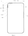
- FIG. 1 is a schematic diagram of an electronic device according to an exemplary embodiment of the present disclosure.
- the electronic device 1 includes a device body 11, a screen 12 and a photo-sensing module 13.
- a light-transmissive area 14 can also be provided between the screen 12 and a side casing 111 of the device body 11.
- the photo-sensing module 13 includes a light emitter 131, a light receiver 132, an emitting circuit 133, and a receiving circuit 134.
- the light emitter 131 is mounted at an edge portion of the device body 11 and corresponds to the light-transmissive area 14.
- the light emitter 131 emits a light, the light can pass out through the light-transmissive area 14 and enters a sensing space 139 corresponding to a front side of the device body, so as to detect an obstacle approaching the front side of the device body.
- the emitting circuit 133 is electrically coupled with the light emitter 131 to control operation of the light emitter 131.
- the receiving circuit 134 is electrically coupled with the light receiver 132 to control operation of the light receiver 132.
- the sensing space 139 refers to an overlapping space of an emitting inverted cone formed by the light emitter 131 and a receiving inverted cone formed by the light receiver 132.
- the screen 12 can cover a portion of the front side of the device body, or cover the whole front side of the device body 11 to exhibit a full-screen display effect.
- the screen 12 can be a special screen, such as a foldable screen, a curved screen, and the like, which is not limited herein.
- the side casing 111 of the device body 11 is a casing of the device body 11 which is fitted with the screen 12 and mounted together with the screen 12.
- the side casing 111 of the device body 11 corresponds to a side portion of the device body 11.
- the light-transmissive area 14 directly faces the front side of the device body, such that light emitted from the light emitter 131 directly faces the sensing space 139corresponding to the front side of the device body.
- the side casing 111 of the device body 11 is a casing which is fitted with the edge of the curve screen and corresponds to the side portion of the device body 11.
- the side casing 111 is aligned with the edge of the curved screen.
- the light emitter 131 and the light receiver 132 of the photo-sensing module 13 can cooperate with a structural member capable of changing a light path, such as a lens, so that a light is emitted towards the sensing space 139 corresponding to the front side of the device body.
- the side casing 111 of the device body 11 is a side casing of an upper device body.
- the light emitter 131 can emit a light through the light-transmissive area 14 for sensing.
- the light emitter 131 does not cause interference on a mounting space for the screen 12.
- the light emitted from the light emitter 131 does not cause interference on display effect of the screen 12.
- the light-transmissive area 14 is arranged between the side casing 111 of the device body and the screen 12, improvement in structures of the screen 12 and the side casing 111 of the device body of the electronic device 1 can be achieved, and difficulties in processing and the cost can be lowered.
- the light-transmissive area 14 can be a hole structure of a preset shape or a structure of a light-transmissive material.
- the present shape of the light-transmissive area 14 can be an elongated stripe, a circle, an oval, and the like, which is not limited herein.
- the light-transmissive area 14 is a hole structure, it can be directly a gap defined between the side casing 111 of the device body and the screen 12 during mounting, which not only increases an amount of the emitted light and improves the sensing effect of the photo-sensing module 13, but simplifies the structures of the screen 12 and the side casing 111 of the device body of the electronic device 1, reducing difficulties in processing and the cost.
- the light-transmissive area 14 is a structure of a light-transmissive material
- the light-transmissive material can satisfy requirements of a light-transmissive effect and improve consistency in appearance of the electronic device 1.
- the emitted light is an infrared light of 850nm/940nm
- the light-transmissive area 14 is made from a light-transmissive material which only allows the infrared light of 850nm/940nm to pass through, the infrared light of 850nm/940nm can pass through the light-transmissive material, and it is can be ensured that the appearance of the present light-transmissive area is consist with those of other structures of the electronic device 1.
- the electronic device 1 can be a mobile phone, a tablet computer, an in-vehicle device, a medical terminal, and the like, which is not limited in the present disclosure.
- the mobile phone is taken as an example of the electronic device 1, a mounting portion of the light receiver 132 and the fitting between the light receiver 132 and the device body 11 are exemplarily illustrated.
- the light emitter 131 of the photo-sensing module 13 can emit an emitted light of a corresponding type. As shown in FIG. 2 , a light path of the emitted light and a light path of the receiving light overlap at an overlap area depicted by dotted lines. Upon the emitted light encounters the obstacle in the overlap area, the receiving light reaches the light receiver 132 and is received by the light receiver 132.
- both the light emitter 131 and the light receiver 132 are mounted at the edge portion of the device body 11 of the mobile phone and correspond to the light-transmissive area 14. Both the emitted light from the light emitter 131 and the receiving light travelling towards the light receiver 132 are transmitted through the light-transmissive area 14, not only a transmitting effect of the emitted light and the receiving light are enhanced, but also interference on a display effect of the screen 12 caused by the light for sensing is avoided.
- the light-transmissive area 14 can be arranged between the side casing 111 at a top portion of the device body and the screen 12, and the light emitter 131 and the light receiver 132 are mounted at the edge portion of the top portion of the device body 11, such that approach of a user's face can be sensed and fed back when the user uses the mobile phone.
- the convenience and light sensitivity of the photo-sensing module 13 can be improved with the light-transmissive area 14 arranged between a top side of the side casing 111 of the device body and the screen 12, and the light emitter 131 and the light receiver 132 mounted at the edge portion of the top portion of the device body 11. All indications of directions, such as left, right, above, below, etc. are defined in a viewing direction of the user.
- the viewing direction of the user is the direction in which the user looks at his electronic device during the regular use of the device, in particular if the device is in the portrait mode (and not in the landscape mode).
- the light-transmissive area 14 can be arranged between the side casing 111 at a bottom portion of the device body and the screen 12, and the light emitter 131 and the light receiver 132 are mounted at the edge portion of the bottom portion of the device body 11, such that approaches of different body portions of the user can be sensed according to different habits when the user uses the electronic device 1.
- the light-transmissive area 14 includes a first area 141 between a first side wall 1111 of the side casing 111 of the device body and the screen 12, and a second area 142 between a second side wall 1112 of the side casing 111 of the device body and the screen 12.
- the first side wall 1111 can be adjacent to the second side wall 1112.
- One of the light receiver 132 and the light emitter 131 corresponds to the first area 141 in portion, and the other one corresponds to the second area 142 in portion.
- the light emitter 131 and the light receiver 132 are arranged at the edge portions of two adjacent sides of the device body 11, so as to improve flexibility of arrangement of a photo-sensing assembly and optimize arrangement of the space in the electronic device 1 for mounting.
- first side wall 1111 or the second side wall 1112 is the side casing 111 at the top portion of the device body.
- the first side wall 1111 is the side casing 111 at the top portion of the device body
- the second side wall 1112 is the side casing 111 at a left side of the device body and adjacent to the side casing 111 at the top portion of the device body.
- the first area 141 is located at a slightly left portion of the top edge of the device body 11
- the second area 142 is located at a slightly upper portion of the left side edge of the device body 11.
- the light emitter 131 corresponds to the second area 142 in portion
- the light receiver 132 corresponds to the first area 141 in portion
- the light path of the emitted light and the light path of the receiving light overlap at the overlap area.
- the receiving light Upon the emitted light encountering the user's face in the overlap area, the receiving light reaches the light receiver 132 and is received by the light receiver 132 to achieve the sensing effect.
- the light-transmissive area 14 at the edge portions of the top portion and the left side of the mobile phone, and the light emitter and the light receiver 132 corresponding to the two areas of the light-transmissive area 14, the trend of the light path and the sensing effect of the photo-sensing module 13, as well as space arrangement of structures in the electronic device 1 are optimized.
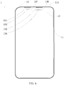
- the light emitter 131 is mounted at an edge portion of the device body 11 and corresponds to the light-transmissive area 14, and the light receiver 132 is mounted below the screen 12.
- the emitted light from the light emitter 131 is transmitted through the light-transmissive area 14, and the receiving light travelling towards the light receiver 132 is transmitted through the screen 12.
- influence on display effect of the screen 12 caused by the emitted light can be avoided, and on the other hand, space occupied by the photo-sensing module 13 in the top space of the mobile phone can be reduced, which provides more space for mounting function assemblies at the top portion of the mobile phone, such as an antenna, a camera module, and the like.
- the photo-sensing module 13 further includes a barrier wall 135, the barrier wall 135 is arranged between the light emitter 131 and the light receiver 132. Since the emitted light is emitted from the light emitter 131, and a reflected light can be formed after the emitted light reaches an inner side wall of the device body 11 and the screen 12, the barrier wall 135 between the light emitter 131 and the light receiver 132 can avoid a ground noise caused by the reflected light reaching the photo-sensing module 13.
- the photo-sensing module 13 can implement sensing based on energy or travel time of the light, which is not limited herein.
- the light emitter 131 can be a vertical cavity surface emitting laser (VCSEL) or an infrared light emitting diode (LED).
- the light receiver 132 can be a photo diode (PD) or a single photon avalanche diode (SPAD which is a photoelectric detection avalanche diode with single photon detection capacity).
- PD photo diode
- SPAD single photon avalanche diode
- the emitted light is laser light.
- the light emitter 131 is the infrared light emitting diode
- the emitted light is infrared light.
- the infrared light can be infrared light of 850nm/940nm.
- a part of the emitted light reflects off a side wall of the device body 11 or other structure of the electronic device 1, in such case, the light reflected back to the photo-sensing module 13 becomes ground noise which affects the sensing effect.
- the photo-sensing module 13 receives less ground noise, while the infrared light emitting diode has large emitting angle with many reflected light paths, the forming probability of ground noise is large.
- the photo-sensing module 13 can monitor intensity or return time of the receiving light by means of the emitting circuit 133 and the receiving circuit 134, to calculate a distance between the obstacle and the electronic device 1. When the distance is smaller than a value, the electronic device 1 is controlled to shut down the screen to avoid touching the screen 12 by mistake and reduce power consumption.
- the emitting circuit 133 and the receiving circuit 134 can be integrated on a first control chip 136, and the first control chip 136 is mounted at an edge portion of the device body 11.
- the emitting circuit 133 and the receiving circuit 134 can be integrated on the same control chip so as to reduce an overall size of the photo-sensing module 13, and the mounting portion at the edge portion of the device body 11 reduces the space in the electronic device 1 occupied by the photo-sensing module 13.
- the emitting circuit 133 and the receiving circuit 134 integrated on the first control chip 136 can also improve convenience in controlling the photo-sensing module 13.
- the emitting circuit 133 can be arranged on a second control chip 137, the receiving circuit 134 is arranged on a third control chip 138, and the second control chip 137 and the third control chip 138 are mounted at the edge portion of the device body 11.
- the second control chip 137 corresponds to the light emitter 131 in portion
- the third control chip 138 corresponds to the light receiver 132 in portion.
- the light emitter 131 can emit a light through the light-transmissive area 14 for sensing.
- the light emitter 131 does not cause interference on a mounting space for the screen 12.
- the light emitted from the light emitter 131 does not cause interference on display effect of the screen 12.
- the light-transmissive area 14 is arranged between the side casing 111 of the device body and the screen 12, improvement in structures of the screen 12 and the side casing 111 of the device body of the electronic device 1 can be reduced, and difficulties in processing and the cost can be lowered.
Landscapes
- Engineering & Computer Science (AREA)
- Theoretical Computer Science (AREA)
- Physics & Mathematics (AREA)
- General Engineering & Computer Science (AREA)
- Computer Hardware Design (AREA)
- General Physics & Mathematics (AREA)
- Human Computer Interaction (AREA)
- Signal Processing (AREA)
- Mathematical Physics (AREA)
- Electromagnetism (AREA)
- Computer Networks & Wireless Communication (AREA)
- Telephone Set Structure (AREA)
Abstract
Description
- The present disclosure generally relates to the field of electronic technologies, and more particularly, to an electronic device.
- In electronic devices, such as mobile phones, it is desirable to minimize the size of a non-display area of a front surface of the electronic device relative to a screen area. This can be accomplished by arranging a light-transmissive hole cooperating with a photosensor in the non-display area or locating a light-transmissive area matching the size of the photosensor on the screen of the electronic device, in order to increase a screen-to-body ratio of the electronic device. However, a display effect of the screen and an aesthetic appearance of the whole device can still be affected by the non-display area with reduced size, and the display effect of the screen is reduced by the light-transmissive area on the screen.
- Embodiments of the present disclosure provide an electronic device that can include a device body, a screen, and a photo-sensing module. The electronic device can futher include a light-transmissive area being provided between the screen and a side casing of the device body. The photo-sensing module can include a light emitter, a light receiver, an emitting circuit, and a receiving circuit, where the emitting circuit is electrically coupled with the light emitter, the receiving circuit is electrically coupled with the light receiver, the light emitter is mounted at an edge portion of the device body and corresponding to the light-transmissive area. An emitted light from the light emitter transmits out through the light-transmissive area and enters a sensing space corresponding to a front side of the device body.
- In some embodiments, the light receiver is mounted at the edge portion of the device body.
- In some embodiments, the light-transmissive area is arranged between the side casing at a top portion of the device body and the screen, and the light emitter and the light receiver are mounted at the edge portion of the top portion of the device body; or the light-transmissive area is arranged between the side casing at a bottom portion of the device body and the screen, and the light emitter and the light receiver are mounted at the edge portion of the bottom portion of the device body.
- In some embodiments, the light-transmissive area includes a first area located between a first side wall of the side casing of the device body and the screen, and a second area located between a second side wall of the side casing of the device body and the screen, the first side wall is adjacent to the second side wall, and one of the light receiver and the light emitter is arranged in the first area, while the other one is arranged in the second area.
- In some embodiments, the first side wall is the side casing at the top portion of the device body, and the second side wall is the side casing at a left side of the device body and adjacent to the side casing at the top portion of the device body; the first area is located at a left portion of the top edge of the device body, the second area is located at an upper portion of the left side edge of the device body.
- In some embodiments, the light receiver is mounted below the screen.
- In some embodiments, the emitting circuit and the receiving circuit are integrated on a first control chip, and the first control chip is mounted at an edge portion of the device body.
- In some embodiments, the emitting circuit is arranged on a second control chip, the receiving circuit is arranged on a third control chip, and the second control chip and the third control chip are mounted at the edge portion of the device body, so that the second control chip is located adjacent to the light emitter, while the third control chip is located adjacent to the light receiver.
- In some embodiments, the photo-sensing module further includes a barrier wall, and the barrier wall is arranged between the light emitter and the light receiver.
- In some embodiments, the light-transmissive area includes a hole structure of a presetshape or a structure of a light-transmissive material.
- In some embodiments, the light-transmissive area further includes a gap between the side casing of the device body and the screen.
- In some embodiments, the screen is a full screen covering the front side of the device body, the side casing of the device body corresponds to a side portion of the device body.
- In some embodiments, the screen is a curve screen, and an edge of the curve screen is bent towards a side of the device body, the side casing of the device body is a casing fitted with the edge of the curve screen and corresponding to a side portion of the device body.
- In some embodiments, the electronic device is of a structure with an upper layer and a lower layer, the upper layer and the lower layer are slidable relative to each other, and the screen is arranged on the upper layer of the electronic device, the side casing of the device body is a side casing of an upper device body.
- In some embodiments, the light-transmissive area is an elongated stripe, a circle, or an oval.
- The technical scheme provided by the embodiments of the present disclosure can have following beneficial effects.
- With the light-transmissive area between the side casing of the device body and the screen, and the light emitter of the photo-sensing module at the edge portion of the device body and corresponding to the portion of the light-transmissive area, the light emitter can emit a light through the light-transmissive area towards the sensing space corresponding to the front side of the device body for sensing. In an aspect regarding a structure, the light emitter does not cause interference on a mounting space for the screen. In an aspect regarding a function, the light emitted from the light emitter does not cause interference on display effect of the screen. In addition, since the light-transmissive area is arranged between the side casing and the screen, improvement in structures of the screen and the casing of the device body of the electronic device can be reduced, and difficulties in processing and the cost are lowered.
- It is to be understood that both the foregoing general description and the following detailed description are exemplary and explanatory only and are not restrictive of the present disclosure.
- The accompanying drawings, which are incorporated in and constitute a part of this specification, illustrate embodiments consistent with the disclosure and, together with the description, serve to explain the principles of the disclosure.
-
FIG. 1 is a schematic diagram of an electronic device according to an exemplary embodiment of the present disclosure. -
FIG. 2 is a schematic diagram of a light path of a photo-sensing module according to an exemplary embodiment of the present disclosure. -
FIG. 3 is a schematic diagram of an electronic device according to another exemplary embodiment of the present disclosure. -
FIG. 4 is a schematic diagram of an electronic device according to still another exemplary embodiment of the present disclosure. -
FIG. 5 is a schematic diagram of a photo-sensing module according to an exemplary embodiment of the present disclosure. -
FIG. 6 is a schematic diagram of an electronic device according to yet another exemplary embodiment of the present disclosure. - Exemplary embodiments of the present disclosure will be described in detail and examples of the embodiments will be illustrated in the drawings. When the following description refers to the drawings, unless specified otherwise, the same numbers in different drawings represent the same or similar elements. The implementations described in the following exemplary embodiments do not represent all implementations consistent with the present disclosure, and instead they are merely examples of devices and methods consistent with aspects of the present disclosure as detailed in the appended claims.
- In the related art, a size of a non-display area of a front surface of an electronic device is usually reduced, and a light-transmissive hole cooperating with a photosensor is defined in the non-display area or a light-transmissive area matching a size of the photosensor is arranged on a screen, in order to increase a screen-to-body ratio of the electronic device, such as a mobile phone. However, a display effect of the screen and an aesthetic appearance of the whole device are still affected due to the existing non-display area even if the size is reduced. The display effect of the screen is reduced with the light-transmissive area, since light is emitted perpendicularly to the light-transmissive area on the screen.
-
FIG. 1 is a schematic diagram of an electronic device according to an exemplary embodiment of the present disclosure. As illustrated inFIG. 1 , theelectronic device 1 includes adevice body 11, ascreen 12 and a photo-sensing module 13. A light-transmissive area 14 can also be provided between thescreen 12 and aside casing 111 of thedevice body 11. The photo-sensing module 13 includes alight emitter 131, alight receiver 132, anemitting circuit 133, and areceiving circuit 134. Thelight emitter 131 is mounted at an edge portion of thedevice body 11 and corresponds to the light-transmissive area 14. - The
light emitter 131 emits a light, the light can pass out through the light-transmissive area 14 and enters asensing space 139 corresponding to a front side of the device body, so as to detect an obstacle approaching the front side of the device body. Theemitting circuit 133 is electrically coupled with thelight emitter 131 to control operation of thelight emitter 131. Thereceiving circuit 134 is electrically coupled with thelight receiver 132 to control operation of thelight receiver 132. Referring toFIGS. 2 and5 , thesensing space 139 refers to an overlapping space of an emitting inverted cone formed by thelight emitter 131 and a receiving inverted cone formed by thelight receiver 132. - The
screen 12 can cover a portion of the front side of the device body, or cover the whole front side of thedevice body 11 to exhibit a full-screen display effect. Alternatively, thescreen 12 can be a special screen, such as a foldable screen, a curved screen, and the like, which is not limited herein. - Corresponding to the type of the screen, the
side casing 111 of thedevice body 11 is a casing of thedevice body 11 which is fitted with thescreen 12 and mounted together with thescreen 12. For example, when thescreen 12 is a full screen covering the front side of the device body, theside casing 111 of thedevice body 11 corresponds to a side portion of thedevice body 11. Accordingly, the light-transmissive area 14 directly faces the front side of the device body, such that light emitted from thelight emitter 131 directly faces the sensing space 139corresponding to the front side of the device body. When thescreen 12 is a curved screen, and an edge of the curved screen is bent towards a side of thedevice body 11, theside casing 111 of thedevice body 11 is a casing which is fitted with the edge of the curve screen and corresponds to the side portion of thedevice body 11. In other words, theside casing 111 is aligned with the edge of the curved screen. Thelight emitter 131 and thelight receiver 132 of the photo-sensing module 13 can cooperate with a structural member capable of changing a light path, such as a lens, so that a light is emitted towards thesensing space 139 corresponding to the front side of the device body. - In addition, when the
electronic device 1 is of a structure with an upper layer and a lower layer which are slidable relative to each other, and thescreen 12 is arranged on the upper layer of the electronic device, theside casing 111 of thedevice body 11 is a side casing of an upper device body. - With the light-
transmissive area 14 between theside casing 111 of thedevice body 11 and thescreen 12, and thelight emitter 131 of the photo-sensing module 13 at the edge portion of thedevice body 11 and corresponding to the portion of the light-transmissive area 14, thelight emitter 131 can emit a light through the light-transmissive area 14 for sensing. In an aspect regarding a structure, thelight emitter 131 does not cause interference on a mounting space for thescreen 12. In an aspect regarding a function, the light emitted from thelight emitter 131 does not cause interference on display effect of thescreen 12. In addition, since the light-transmissive area 14 is arranged between theside casing 111 of the device body and thescreen 12, improvement in structures of thescreen 12 and theside casing 111 of the device body of theelectronic device 1 can be achieved, and difficulties in processing and the cost can be lowered. - It should be noted that, the light-
transmissive area 14 can be a hole structure of a preset shape or a structure of a light-transmissive material. The present shape of the light-transmissive area 14 can be an elongated stripe, a circle, an oval, and the like, which is not limited herein. When the light-transmissive area 14 is a hole structure, it can be directly a gap defined between theside casing 111 of the device body and thescreen 12 during mounting, which not only increases an amount of the emitted light and improves the sensing effect of the photo-sensingmodule 13, but simplifies the structures of thescreen 12 and theside casing 111 of the device body of theelectronic device 1, reducing difficulties in processing and the cost. - When the light-
transmissive area 14 is a structure of a light-transmissive material, the light-transmissive material can satisfy requirements of a light-transmissive effect and improve consistency in appearance of theelectronic device 1. For example, when the emitted light is an infrared light of 850nm/940nm, the light-transmissive area 14 is made from a light-transmissive material which only allows the infrared light of 850nm/940nm to pass through, the infrared light of 850nm/940nm can pass through the light-transmissive material, and it is can be ensured that the appearance of the present light-transmissive area is consist with those of other structures of theelectronic device 1. - In the above embodiments, the
electronic device 1 can be a mobile phone, a tablet computer, an in-vehicle device, a medical terminal, and the like, which is not limited in the present disclosure. In the following, the mobile phone is taken as an example of theelectronic device 1, a mounting portion of thelight receiver 132 and the fitting between thelight receiver 132 and thedevice body 11 are exemplarily illustrated. - The
light emitter 131 of the photo-sensingmodule 13 can emit an emitted light of a corresponding type. As shown inFIG. 2 , a light path of the emitted light and a light path of the receiving light overlap at an overlap area depicted by dotted lines. Upon the emitted light encounters the obstacle in the overlap area, the receiving light reaches thelight receiver 132 and is received by thelight receiver 132. - In an embodiment, as shown in
FIG. 1 , both thelight emitter 131 and thelight receiver 132 are mounted at the edge portion of thedevice body 11 of the mobile phone and correspond to the light-transmissive area 14. Both the emitted light from thelight emitter 131 and the receiving light travelling towards thelight receiver 132 are transmitted through the light-transmissive area 14, not only a transmitting effect of the emitted light and the receiving light are enhanced, but also interference on a display effect of thescreen 12 caused by the light for sensing is avoided. - The light-
transmissive area 14 can be arranged between theside casing 111 at a top portion of the device body and thescreen 12, and thelight emitter 131 and thelight receiver 132 are mounted at the edge portion of the top portion of thedevice body 11, such that approach of a user's face can be sensed and fed back when the user uses the mobile phone. - Specifically, when the user gets talks on the mobile phone, his face approaches the front side of the
device body 11, he aligns his ear with a receiver on the top portion of the mobile phone and aligns his mouth with a microphone on a bottom portion of the mobile phone. The area and probability that the light is shielded at the edge portion of the top portion of the mobile phone are large based on the above usage habits, the convenience and light sensitivity of the photo-sensingmodule 13 can be improved with the light-transmissive area 14 arranged between a top side of theside casing 111 of the device body and thescreen 12, and thelight emitter 131 and thelight receiver 132 mounted at the edge portion of the top portion of thedevice body 11. All indications of directions, such as left, right, above, below, etc. are defined in a viewing direction of the user. The viewing direction of the user is the direction in which the user looks at his electronic device during the regular use of the device, in particular if the device is in the portrait mode (and not in the landscape mode). - Alternatively, the light-
transmissive area 14 can be arranged between theside casing 111 at a bottom portion of the device body and thescreen 12, and thelight emitter 131 and thelight receiver 132 are mounted at the edge portion of the bottom portion of thedevice body 11, such that approaches of different body portions of the user can be sensed according to different habits when the user uses theelectronic device 1. - Alternatively, as shown in
FIG. 3 , the light-transmissive area 14 includes afirst area 141 between afirst side wall 1111 of theside casing 111 of the device body and thescreen 12, and asecond area 142 between asecond side wall 1112 of theside casing 111 of the device body and thescreen 12. As shown, thefirst side wall 1111 can be adjacent to thesecond side wall 1112. One of thelight receiver 132 and thelight emitter 131 corresponds to thefirst area 141 in portion, and the other one corresponds to thesecond area 142 in portion. Thelight emitter 131 and thelight receiver 132 are arranged at the edge portions of two adjacent sides of thedevice body 11, so as to improve flexibility of arrangement of a photo-sensing assembly and optimize arrangement of the space in theelectronic device 1 for mounting. - Furthermore, the
first side wall 1111 or thesecond side wall 1112 is theside casing 111 at the top portion of the device body. For instance, thefirst side wall 1111 is theside casing 111 at the top portion of the device body, and thesecond side wall 1112 is theside casing 111 at a left side of the device body and adjacent to theside casing 111 at the top portion of the device body. Thefirst area 141 is located at a slightly left portion of the top edge of thedevice body 11, thesecond area 142 is located at a slightly upper portion of the left side edge of thedevice body 11. Thelight emitter 131 corresponds to thesecond area 142 in portion, thelight receiver 132 corresponds to thefirst area 141 in portion, and the light path of the emitted light and the light path of the receiving light overlap at the overlap area. - Upon the emitted light encountering the user's face in the overlap area, the receiving light reaches the
light receiver 132 and is received by thelight receiver 132 to achieve the sensing effect. With the light-transmissive area 14 at the edge portions of the top portion and the left side of the mobile phone, and the light emitter and thelight receiver 132 corresponding to the two areas of the light-transmissive area 14, the trend of the light path and the sensing effect of the photo-sensingmodule 13, as well as space arrangement of structures in theelectronic device 1 are optimized. - In another embodiment, as shown in
FIG. 4 , thelight emitter 131 is mounted at an edge portion of thedevice body 11 and corresponds to the light-transmissive area 14, and thelight receiver 132 is mounted below thescreen 12. The emitted light from thelight emitter 131 is transmitted through the light-transmissive area 14, and the receiving light travelling towards thelight receiver 132 is transmitted through thescreen 12. On the one hand, influence on display effect of thescreen 12 caused by the emitted light can be avoided, and on the other hand, space occupied by the photo-sensingmodule 13 in the top space of the mobile phone can be reduced, which provides more space for mounting function assemblies at the top portion of the mobile phone, such as an antenna, a camera module, and the like. - In addition, as shown in
FIG. 5 , the photo-sensingmodule 13 further includes abarrier wall 135, thebarrier wall 135 is arranged between thelight emitter 131 and thelight receiver 132. Since the emitted light is emitted from thelight emitter 131, and a reflected light can be formed after the emitted light reaches an inner side wall of thedevice body 11 and thescreen 12, thebarrier wall 135 between thelight emitter 131 and thelight receiver 132 can avoid a ground noise caused by the reflected light reaching the photo-sensingmodule 13. - The photo-sensing
module 13 can implement sensing based on energy or travel time of the light, which is not limited herein. For example, thelight emitter 131 can be a vertical cavity surface emitting laser (VCSEL) or an infrared light emitting diode (LED). Thelight receiver 132 can be a photo diode (PD) or a single photon avalanche diode (SPAD which is a photoelectric detection avalanche diode with single photon detection capacity). When thelight emitter 131 is a VCSEL, the emitted light is laser light. When thelight emitter 131 is the infrared light emitting diode, the emitted light is infrared light. Particularly, the infrared light can be infrared light of 850nm/940nm. During operation of the light emitter, a part of the emitted light reflects off a side wall of thedevice body 11 or other structure of theelectronic device 1, in such case, the light reflected back to the photo-sensingmodule 13 becomes ground noise which affects the sensing effect. Because the VCSEL has a small emitting angle and concentrated emitting energy with less reflected light, the photo-sensingmodule 13 receives less ground noise, while the infrared light emitting diode has large emitting angle with many reflected light paths, the forming probability of ground noise is large. - Regarding the mounting position of two types of the
light receiver 132, when the receiving light is received, the photo-sensingmodule 13 can monitor intensity or return time of the receiving light by means of the emittingcircuit 133 and the receivingcircuit 134, to calculate a distance between the obstacle and theelectronic device 1. When the distance is smaller than a value, theelectronic device 1 is controlled to shut down the screen to avoid touching thescreen 12 by mistake and reduce power consumption. - As shown in an embodiment of
FIG. 5 , the emittingcircuit 133 and the receivingcircuit 134 can be integrated on afirst control chip 136, and thefirst control chip 136 is mounted at an edge portion of thedevice body 11. The emittingcircuit 133 and the receivingcircuit 134 can be integrated on the same control chip so as to reduce an overall size of the photo-sensingmodule 13, and the mounting portion at the edge portion of thedevice body 11 reduces the space in theelectronic device 1 occupied by the photo-sensingmodule 13. Further, the emittingcircuit 133 and the receivingcircuit 134 integrated on thefirst control chip 136 can also improve convenience in controlling the photo-sensingmodule 13. - In an embodiment shown in
FIG. 6 , the emittingcircuit 133 can be arranged on asecond control chip 137, the receivingcircuit 134 is arranged on athird control chip 138, and thesecond control chip 137 and thethird control chip 138 are mounted at the edge portion of thedevice body 11. Thesecond control chip 137 corresponds to thelight emitter 131 in portion, and thethird control chip 138 corresponds to thelight receiver 132 in portion. Separately arrangement of the emittingcircuit 133 and the receivingcircuit 134 makes it convenient for mounting and cooperation between thesecond control chip 137 and thelight emitter 131, and between thethird control chip 138 and thelight receiver 132, thereby improving flexibility in mounting structures and convenience of test and maintenance of circuits. - With the light-
transmissive area 14 between theside casing 111 of thedevice body 11 and thescreen 12, and thelight emitter 131 of the photo-sensingmodule 13 at the edge portion of thedevice body 11 and corresponding to the portion of the light-transmissive area 14, thelight emitter 131 can emit a light through the light-transmissive area 14 for sensing. In an aspect regarding a structure, thelight emitter 131 does not cause interference on a mounting space for thescreen 12. In an aspect regarding a function, the light emitted from thelight emitter 131 does not cause interference on display effect of thescreen 12. In addition, since the light-transmissive area 14 is arranged between theside casing 111 of the device body and thescreen 12, improvement in structures of thescreen 12 and theside casing 111 of the device body of theelectronic device 1 can be reduced, and difficulties in processing and the cost can be lowered. - Other embodiments of the disclosure will be apparent to those skilled in the art from consideration of the specification and practice of the technical solutions disclosed here. This application is intended to cover any variations, uses, or adaptations of the disclosure following the general principles thereof and including such departures from the present disclosure as come within known or customary practice in the art.
Claims (15)
- An electronic device (1), comprising:a device body (11) having a side casing (111);a screen (12) that is mounted to the device body (11);a light-transmissive area (14) that is arranged between the screen (12) and the side casing (111) of the device body (11); anda photo-sensing module (13) that includes a light emitter (131), a light receiver (132),an emitting circuit (133), and a receiving circuit (134), where:the emitting circuit (133) is electrically coupled with the light emitter (131),the receiving circuit (134) is electrically coupled with the light receiver (132),the light emitter (131) is mounted at an edge portion of the device body (11) that corresponds to the light-transmissive area (14), andwherein light emitted from the light emitter (131) passes out through the light-transmissive area (14) into a sensing space (139) that corresponds to a front side of the device body (11).
- The electronic device (1) according to claim 1, wherein the light receiver (132) is mounted at the edge portion of the device body (11).
- The electronic device (1) according to claim 2, wherein:the light-transmissive area (14) is arranged between the side casing (111) at a top portion of the device body (11) and the screen (12), and the light emitter (131) and the light receiver (132) are mounted at the edge portion of the top portion of the device body (11); orthe light-transmissive area (14) is arranged between the side casing (111) at a bottom portion of the device body (11) and the screen (12), and the light emitter (131) and the light receiver (132) are mounted at the edge portion of the bottom portion of the device body (11).
- The electronic device (1) according to claim 2, wherein the light-transmissive area (14) comprises:a first area (141) located between a first side wall (1111) of the side casing (111) of the device body (11) and the screen (12), anda second area (142) located between a second side wall (1112) of the side casing (111) of the device body (11) and the screen (12),wherein the first side wall (1111) is adjacent to the second side wall (1112), and one of the light receiver (132) and the light emitter (131) is arranged in the first area (141), while the other one is arranged in the second area (142).
- The electronic device (1) according to claim 4, wherein the first side wall (1111) is the side casing (111) at the top portion of the device body (11), and the second side wall (1112) is the side casing (111) at a left side of the device body (11) and adjacent to the side casing (111) at the top portion of the device body (11); the first area (141) is located at a left portion of the top edge of the device body (11), the second area (142) is located at an upper portion of the left side edge of the device body (11).
- The electronic device (1) according to claim 1, wherein the light receiver (132) is mounted below the screen (12).
- The electronic device (1) according to any one of claims 1 to 6, wherein the emitting circuit (133) and the receiving circuit (134) are integrated on a first control chip (136), and the first control chip (136) is mounted at the edge portion of the device body (11).
- The electronic device (1) according to any one of claims 1 to 6, wherein:the emitting circuit (133) is arranged on a second control chip (137),the receiving circuit (134) is arranged on a third control chip (138), andthe second control chip (137) and the third control chip (138) are mounted at the edge portion of the device body (11), so that the second control chip (137) is located adjacent to the light emitter (131), while the third control chip (138) is adjacent to the light receiver (132).
- The electronic device (1) according to any one of claims 1 to 8, wherein the photo-sensing module (13) further includes a barrier wall (135), and the barrier wall (135) is arranged between the light emitter (131) and the light receiver (132).
- The electronic device (1) according to any one of claims 1 to 9, wherein the light-transmissive area (14) includes a hole structure of a preset shape or a structure of a light-transmissive material.
- The electronic device (1) according to claim 10, wherein the light-transmissive area (14) further comprises a gap between the screen (12) and the side casing (111) of the device body (11).
- The electronic device (1) according to any one of claims 1 to 11, wherein the screen (12) is a full screen covering the front side of the device body (11), the side casing (111) of the device body (11) corresponds to a side portion of the device body (11).
- The electronic device (1) according to any one of claims 1 to 11, wherein the screen (12) is a curve screen, and an edge of the curve screen is bent towards a side of the device body (11), the side casing (111) of the device body (11) is a casing fitted with the edge of the curve screen and corresponding to a side portion of the device body (11).
- The electronic device (1) according to any one of claims 1 to 11, wherein the electronic device (1) is of a structure with an upper layer and a lower layer, the upper layer and the lower layer are slidable relative to each other, and the screen (12) is arranged on the upper layer of the electronic device (1), the side casing (111) of the device body (11) is a side casing (111) of an upper device body (11).
- The electronic device (1) according to any one of claims 1 to 14, wherein the light-transmissive area (14) is an elongated stripe, a circle, or an oval.
Applications Claiming Priority (1)
| Application Number | Priority Date | Filing Date | Title |
|---|---|---|---|
| CN201910487543.3A CN112055101A (en) | 2019-06-05 | 2019-06-05 | Electronic equipment |
Publications (1)
| Publication Number | Publication Date |
|---|---|
| EP3748872A1 true EP3748872A1 (en) | 2020-12-09 |
Family
ID=70333856
Family Applications (1)
| Application Number | Title | Priority Date | Filing Date |
|---|---|---|---|
| EP20170331.1A Withdrawn EP3748872A1 (en) | 2019-06-05 | 2020-04-20 | Electronic device |
Country Status (3)
| Country | Link |
|---|---|
| US (1) | US11150767B2 (en) |
| EP (1) | EP3748872A1 (en) |
| CN (1) | CN112055101A (en) |
Families Citing this family (2)
| Publication number | Priority date | Publication date | Assignee | Title |
|---|---|---|---|---|
| CN112822315A (en) * | 2021-02-25 | 2021-05-18 | 北京小米移动软件有限公司 | Mobile terminal |
| CN114335391B (en) * | 2021-12-30 | 2024-02-02 | 武汉天马微电子有限公司 | A display panel and its manufacturing method and display device |
Citations (7)
| Publication number | Priority date | Publication date | Assignee | Title |
|---|---|---|---|---|
| WO2017075005A1 (en) * | 2015-10-30 | 2017-05-04 | Essential Products, Inc. | System and method for reducing the number of ports associated with a mobile device |
| CN108462769A (en) * | 2018-03-09 | 2018-08-28 | 广东欧珀移动通信有限公司 | Electronic device and its manufacturing method |
| CN108540600A (en) * | 2018-03-30 | 2018-09-14 | 广东欧珀移动通信有限公司 | Electronic device |
| CN108600419A (en) * | 2018-03-09 | 2018-09-28 | 广东欧珀移动通信有限公司 | Electronic device and its manufacturing method |
| CN108989494A (en) * | 2018-06-27 | 2018-12-11 | 北京小米移动软件有限公司 | A kind of electronic equipment |
| CN208386629U (en) * | 2018-06-02 | 2019-01-15 | Oppo广东移动通信有限公司 | Electronic equipment |
| CN109274787A (en) * | 2018-08-21 | 2019-01-25 | Oppo广东移动通信有限公司 | Electronic device |
Family Cites Families (14)
| Publication number | Priority date | Publication date | Assignee | Title |
|---|---|---|---|---|
| KR20170049280A (en) * | 2015-10-28 | 2017-05-10 | 엘지전자 주식회사 | Mobile terminal and a method of controlling the same |
| KR102419624B1 (en) * | 2016-01-21 | 2022-07-11 | 삼성전자 주식회사 | Arrangement structure of sensor of electronic apparatus |
| CN106933415B (en) * | 2017-03-07 | 2019-11-26 | Oppo广东移动通信有限公司 | Sensor assembly and terminal |
| EP3982618B1 (en) * | 2017-04-25 | 2023-03-15 | Huawei Technologies Co., Ltd. | Electronic device with lcd display |
| US10268234B2 (en) * | 2017-08-07 | 2019-04-23 | Apple Inc. | Bracket assembly for a multi-component vision system in an electronic device |
| CN207530869U (en) * | 2017-11-06 | 2018-06-22 | 维沃移动通信有限公司 | A kind of mobile terminal |
| TWI651660B (en) * | 2017-12-12 | 2019-02-21 | 財團法人工業技術研究院 | Fingerprint identification device |
| CN108540595B (en) * | 2018-03-09 | 2021-02-12 | Oppo广东移动通信有限公司 | Electronic device and method for manufacturing the same |
| CN111984155B (en) * | 2018-03-09 | 2023-07-18 | Oppo广东移动通信有限公司 | Electronic device and manufacturing method thereof |
| CN108769296B (en) * | 2018-03-21 | 2020-08-07 | Oppo广东移动通信有限公司 | Electronic device and method of manufacturing the same |
| CN108712523A (en) * | 2018-03-30 | 2018-10-26 | 广东欧珀移动通信有限公司 | Electronic device and method for manufacturing the same |
| CN208721790U (en) * | 2018-05-29 | 2019-04-09 | 维沃移动通信有限公司 | A kind of terminal device |
| CN109087581A (en) * | 2018-07-12 | 2018-12-25 | 维沃移动通信有限公司 | a mobile terminal |
| CN108898951A (en) * | 2018-07-27 | 2018-11-27 | 维沃移动通信有限公司 | a mobile terminal |
-
2019
- 2019-06-05 CN CN201910487543.3A patent/CN112055101A/en active Pending
- 2019-11-27 US US16/698,243 patent/US11150767B2/en active Active
-
2020
- 2020-04-20 EP EP20170331.1A patent/EP3748872A1/en not_active Withdrawn
Patent Citations (8)
| Publication number | Priority date | Publication date | Assignee | Title |
|---|---|---|---|---|
| WO2017075005A1 (en) * | 2015-10-30 | 2017-05-04 | Essential Products, Inc. | System and method for reducing the number of ports associated with a mobile device |
| CN108462769A (en) * | 2018-03-09 | 2018-08-28 | 广东欧珀移动通信有限公司 | Electronic device and its manufacturing method |
| CN108600419A (en) * | 2018-03-09 | 2018-09-28 | 广东欧珀移动通信有限公司 | Electronic device and its manufacturing method |
| CN108540600A (en) * | 2018-03-30 | 2018-09-14 | 广东欧珀移动通信有限公司 | Electronic device |
| CN208386629U (en) * | 2018-06-02 | 2019-01-15 | Oppo广东移动通信有限公司 | Electronic equipment |
| CN108989494A (en) * | 2018-06-27 | 2018-12-11 | 北京小米移动软件有限公司 | A kind of electronic equipment |
| CN109274787A (en) * | 2018-08-21 | 2019-01-25 | Oppo广东移动通信有限公司 | Electronic device |
| WO2020038033A1 (en) * | 2018-08-21 | 2020-02-27 | Oppo广东移动通信有限公司 | Electronic device |
Also Published As
| Publication number | Publication date |
|---|---|
| US11150767B2 (en) | 2021-10-19 |
| CN112055101A (en) | 2020-12-08 |
| US20200387262A1 (en) | 2020-12-10 |
Similar Documents
| Publication | Publication Date | Title |
|---|---|---|
| US10650789B2 (en) | Method and apparatus for controlling display screen statuses | |
| EP3490233B1 (en) | Proximity sensor partially behind the touch-screen | |
| CN108769296B (en) | Electronic device and method of manufacturing the same | |
| US10403232B2 (en) | Method of controlling display screen states, and apparatus | |
| CN106850989A (en) | Display screen condition control method and device | |
| CN107064948B (en) | Sensor module and mobile terminal | |
| EP3748872A1 (en) | Electronic device | |
| CN111984155B (en) | Electronic device and manufacturing method thereof | |
| CN106444997A (en) | Sensor component, cover plate component and mobile terminal | |
| US20180292568A1 (en) | Optical proximity sensor with a self-integrated barrier | |
| CN108833615B (en) | Electronic device | |
| CN206442435U (en) | Sensor cluster and mobile terminal | |
| CN212727096U (en) | Terminal and light guide thereof | |
| CN213903860U (en) | Electronic equipment | |
| CN106774656B (en) | Sensor component, cover plate, mobile terminal and terminal control method | |
| CN108540600B (en) | electronic device | |
| US20210072357A1 (en) | Electronic device | |
| EP3748411B1 (en) | Electronic device | |
| CN106686215A (en) | Sensor components and mobile terminals | |
| CN206930977U (en) | Sensor cluster, cover plate assembly and mobile terminal | |
| EP4125261B1 (en) | Electronic device | |
| CN108521481B (en) | Electronic device | |
| CN111245978B (en) | Mobile terminal | |
| CN207115242U (en) | Sensor cluster, cover plate and mobile terminal | |
| CN112732012A (en) | Electronic device |
Legal Events
| Date | Code | Title | Description |
|---|---|---|---|
| PUAI | Public reference made under article 153(3) epc to a published international application that has entered the european phase |
Free format text: ORIGINAL CODE: 0009012 |
|
| STAA | Information on the status of an ep patent application or granted ep patent |
Free format text: STATUS: THE APPLICATION HAS BEEN PUBLISHED |
|
| AK | Designated contracting states |
Kind code of ref document: A1 Designated state(s): AL AT BE BG CH CY CZ DE DK EE ES FI FR GB GR HR HU IE IS IT LI LT LU LV MC MK MT NL NO PL PT RO RS SE SI SK SM TR |
|
| AX | Request for extension of the european patent |
Extension state: BA ME |
|
| STAA | Information on the status of an ep patent application or granted ep patent |
Free format text: STATUS: REQUEST FOR EXAMINATION WAS MADE |
|
| 17P | Request for examination filed |
Effective date: 20210609 |
|
| RBV | Designated contracting states (corrected) |
Designated state(s): AL AT BE BG CH CY CZ DE DK EE ES FI FR GB GR HR HU IE IS IT LI LT LU LV MC MK MT NL NO PL PT RO RS SE SI SK SM TR |
|
| STAA | Information on the status of an ep patent application or granted ep patent |
Free format text: STATUS: EXAMINATION IS IN PROGRESS |
|
| 17Q | First examination report despatched |
Effective date: 20230102 |
|
| GRAP | Despatch of communication of intention to grant a patent |
Free format text: ORIGINAL CODE: EPIDOSNIGR1 |
|
| STAA | Information on the status of an ep patent application or granted ep patent |
Free format text: STATUS: GRANT OF PATENT IS INTENDED |
|
| INTG | Intention to grant announced |
Effective date: 20241125 |
|
| STAA | Information on the status of an ep patent application or granted ep patent |
Free format text: STATUS: THE APPLICATION IS DEEMED TO BE WITHDRAWN |
|
| 18D | Application deemed to be withdrawn |
Effective date: 20250326 |