EP3748830A1 - Power converter with snubber circuit - Google Patents
Power converter with snubber circuit Download PDFInfo
- Publication number
- EP3748830A1 EP3748830A1 EP20178330.5A EP20178330A EP3748830A1 EP 3748830 A1 EP3748830 A1 EP 3748830A1 EP 20178330 A EP20178330 A EP 20178330A EP 3748830 A1 EP3748830 A1 EP 3748830A1
- Authority
- EP
- European Patent Office
- Prior art keywords
- circuitry
- coil
- converter
- snubber
- parallel
- Prior art date
- Legal status (The legal status is an assumption and is not a legal conclusion. Google has not performed a legal analysis and makes no representation as to the accuracy of the status listed.)
- Granted
Links
Images


Classifications
-
- H—ELECTRICITY
- H02—GENERATION; CONVERSION OR DISTRIBUTION OF ELECTRIC POWER
- H02M—APPARATUS FOR CONVERSION BETWEEN AC AND AC, BETWEEN AC AND DC, OR BETWEEN DC AND DC, AND FOR USE WITH MAINS OR SIMILAR POWER SUPPLY SYSTEMS; CONVERSION OF DC OR AC INPUT POWER INTO SURGE OUTPUT POWER; CONTROL OR REGULATION THEREOF
- H02M1/00—Details of apparatus for conversion
- H02M1/32—Means for protecting converters other than automatic disconnection
- H02M1/34—Snubber circuits
-
- H—ELECTRICITY
- H02—GENERATION; CONVERSION OR DISTRIBUTION OF ELECTRIC POWER
- H02M—APPARATUS FOR CONVERSION BETWEEN AC AND AC, BETWEEN AC AND DC, OR BETWEEN DC AND DC, AND FOR USE WITH MAINS OR SIMILAR POWER SUPPLY SYSTEMS; CONVERSION OF DC OR AC INPUT POWER INTO SURGE OUTPUT POWER; CONTROL OR REGULATION THEREOF
- H02M3/00—Conversion of DC power input into DC power output
- H02M3/22—Conversion of DC power input into DC power output with intermediate conversion into AC
- H02M3/24—Conversion of DC power input into DC power output with intermediate conversion into AC by static converters
- H02M3/28—Conversion of DC power input into DC power output with intermediate conversion into AC by static converters using discharge tubes with control electrode or semiconductor devices with control electrode to produce the intermediate AC
- H02M3/325—Conversion of DC power input into DC power output with intermediate conversion into AC by static converters using discharge tubes with control electrode or semiconductor devices with control electrode to produce the intermediate AC using devices of a triode or a transistor type requiring continuous application of a control signal
- H02M3/335—Conversion of DC power input into DC power output with intermediate conversion into AC by static converters using discharge tubes with control electrode or semiconductor devices with control electrode to produce the intermediate AC using devices of a triode or a transistor type requiring continuous application of a control signal using semiconductor devices only
- H02M3/33507—Conversion of DC power input into DC power output with intermediate conversion into AC by static converters using discharge tubes with control electrode or semiconductor devices with control electrode to produce the intermediate AC using devices of a triode or a transistor type requiring continuous application of a control signal using semiconductor devices only with automatic control of the output voltage or current, e.g. flyback converters
-
- H—ELECTRICITY
- H02—GENERATION; CONVERSION OR DISTRIBUTION OF ELECTRIC POWER
- H02M—APPARATUS FOR CONVERSION BETWEEN AC AND AC, BETWEEN AC AND DC, OR BETWEEN DC AND DC, AND FOR USE WITH MAINS OR SIMILAR POWER SUPPLY SYSTEMS; CONVERSION OF DC OR AC INPUT POWER INTO SURGE OUTPUT POWER; CONTROL OR REGULATION THEREOF
- H02M1/00—Details of apparatus for conversion
- H02M1/0067—Converter structures employing plural converter units, other than for parallel operation of the units on a single load
- H02M1/008—Plural converter units for generating at two or more independent and non-parallel outputs, e.g. systems with plural point of load switching regulators
-
- H—ELECTRICITY
- H02—GENERATION; CONVERSION OR DISTRIBUTION OF ELECTRIC POWER
- H02M—APPARATUS FOR CONVERSION BETWEEN AC AND AC, BETWEEN AC AND DC, OR BETWEEN DC AND DC, AND FOR USE WITH MAINS OR SIMILAR POWER SUPPLY SYSTEMS; CONVERSION OF DC OR AC INPUT POWER INTO SURGE OUTPUT POWER; CONTROL OR REGULATION THEREOF
- H02M1/00—Details of apparatus for conversion
- H02M1/32—Means for protecting converters other than automatic disconnection
- H02M1/34—Snubber circuits
- H02M1/346—Passive non-dissipative snubbers
-
- H—ELECTRICITY
- H02—GENERATION; CONVERSION OR DISTRIBUTION OF ELECTRIC POWER
- H02M—APPARATUS FOR CONVERSION BETWEEN AC AND AC, BETWEEN AC AND DC, OR BETWEEN DC AND DC, AND FOR USE WITH MAINS OR SIMILAR POWER SUPPLY SYSTEMS; CONVERSION OF DC OR AC INPUT POWER INTO SURGE OUTPUT POWER; CONTROL OR REGULATION THEREOF
- H02M3/00—Conversion of DC power input into DC power output
- H02M3/22—Conversion of DC power input into DC power output with intermediate conversion into AC
- H02M3/24—Conversion of DC power input into DC power output with intermediate conversion into AC by static converters
- H02M3/28—Conversion of DC power input into DC power output with intermediate conversion into AC by static converters using discharge tubes with control electrode or semiconductor devices with control electrode to produce the intermediate AC
- H02M3/325—Conversion of DC power input into DC power output with intermediate conversion into AC by static converters using discharge tubes with control electrode or semiconductor devices with control electrode to produce the intermediate AC using devices of a triode or a transistor type requiring continuous application of a control signal
- H02M3/335—Conversion of DC power input into DC power output with intermediate conversion into AC by static converters using discharge tubes with control electrode or semiconductor devices with control electrode to produce the intermediate AC using devices of a triode or a transistor type requiring continuous application of a control signal using semiconductor devices only
-
- Y—GENERAL TAGGING OF NEW TECHNOLOGICAL DEVELOPMENTS; GENERAL TAGGING OF CROSS-SECTIONAL TECHNOLOGIES SPANNING OVER SEVERAL SECTIONS OF THE IPC; TECHNICAL SUBJECTS COVERED BY FORMER USPC CROSS-REFERENCE ART COLLECTIONS [XRACs] AND DIGESTS
- Y02—TECHNOLOGIES OR APPLICATIONS FOR MITIGATION OR ADAPTATION AGAINST CLIMATE CHANGE
- Y02B—CLIMATE CHANGE MITIGATION TECHNOLOGIES RELATED TO BUILDINGS, e.g. HOUSING, HOUSE APPLIANCES OR RELATED END-USER APPLICATIONS
- Y02B70/00—Technologies for an efficient end-user side electric power management and consumption
- Y02B70/10—Technologies improving the efficiency by using switched-mode power supplies [SMPS], i.e. efficient power electronics conversion e.g. power factor correction or reduction of losses in power supplies or efficient standby modes
Definitions
- Exemplary embodiments pertain to the art of power converter snubber circuits.
- Switched-mode power supplies may incur voltage spikes during switching operations.
- Snubber circuits may be implemented to reduce such transients.
- the power conversion circuitry includes a converter coil.
- the power conversion circuitry includes a power source.
- the power conversion circuitry includes a switch connected to the converter coil to control current flowing through the converter coil from the power source, the power conversion circuitry including a converter output connectable to a converter load.
- the power conversion circuitry includes parallel snubber circuitry having resonant circuitry connected in parallel with the converter coil, the resonant circuitry including a parallel snubber circuitry coil and a capacitor connected in series, the parallel snubber circuitry including a parallel snubber output connectable to a parallel snubber circuitry load.
- further embodiments may include that the parallel snubber circuitry coil is a first parallel coil of the parallel snubber circuitry, and further comprising, a second parallel coil associated with the first parallel coil to form a parallel snubber circuitry transformer.
- further embodiments may include that the parallel snubber circuitry transformer is configured to supply power to the parallel snubber circuitry load associated with the parallel snubber circuitry transformer.
- further embodiments may include that the parallel snubber circuitry transformer has a winding ratio of 9:4 between the first parallel coil and the second parallel coil.
- further embodiments may include a parallel snubber diode is disposed on a conductive path between the converter coil and the parallel snubber circuitry coil and biased to enable less restrictive current flow from the parallel snubber circuitry coil to the converter coil than from the converter coil to the parallel snubber circuitry coil.
- further embodiments may include that the switch is associated with a predefined oscillation frequency greater than a resonant frequency of the capacitor and the parallel snubber circuitry coil.
- further embodiments may include that the capacitor has a capacitance of five microfarads and the parallel snubber circuitry coil has an inductance of 10 microhenries.
- further embodiments may include that the parallel snubber circuitry coil is bifilar having a first winding portion and a second winding portion.
- further embodiments may include that the first winding portion and the second winding portion have a combined inductance of 10 microhenries.
- further embodiments may include series snubber circuitry associated with the converter coil including a series inductor disposed in series with the converter coil and the capacitor with respect to the power source, and a series snubber diode disposed between the parallel and the converter coil.
- further embodiments may include series snubber circuitry associated with the converter coil including a low dropout voltage regulator in series with the converter coil with respect to the power source.
- further embodiments may include that series snubber circuitry associated with the converter coil including a flyback transformer in series with the converter coil with respect to the power source.
- further embodiments may include that the series snubber circuitry has a series snubber circuitry voltage output with a series snubber circuitry voltage polarity opposite a power conversion circuitry polarity of the power conversion circuitry such that a power converter output voltage of the power converter is less the series snubber circuitry voltage output.
- further embodiments may include that the flyback transformer includes a load side having series snubber circuitry secondary winding, a series snubber circuitry load, and a series snubber diode disposed is biased to enable less restrictive current flow from the series snubber circuitry load to the series snubber circuitry secondary winding than from the series snubber circuitry secondary winding to the series snubber circuitry load.
- further embodiments may include series snubber circuitry having a series snubber circuitry output configured in series with a parallel snubber circuitry output of the parallel snubber circuitry in series with the converter output.
- further embodiments may include that the series snubber circuitry includes a series snubber circuitry transformer having a winding ratio of 13:5 between a first series snubber winding and a second series snubber winding.
- further embodiments may include that the power conversion circuitry includes a power conversion transformer having a winding ratio of 13:5 between a first power conversion winding and a second power conversion winding.
- controller circuitry operable to oscillate the switch between an open position and a closed position according to a predetermined output voltage command associated with the power converter.
- a power converter including power conversion circuitry including a converter coil associated with a power supply and a switch configured with a power conversion circuitry output to a converter load associated with the power converter.
- the power converter includes parallel snubber circuitry associated with the converter coil having a parallel snubber circuitry coil disposed in parallel with the converter coil with respect to the power supply, a parallel snubber diode disposed between the parallel snubber circuitry coil and the converter coil biased to enable less restrictive current flow from the parallel snubber circuitry coil to the converter coil than from the converter coil to the parallel snubber circuitry coil, and a capacitor disposed between the parallel snubber circuitry coil and the converter coil.
- a power converter including power conversion circuitry including a converter coil associated with a power supply and a switch configured with a power conversion circuitry output to a converter load associated with the power converter.
- the power converter includes parallel snubber circuitry associated with the converter coil having a parallel snubber circuitry coil disposed in parallel with the converter coil with respect to the power supply, a parallel snubber diode disposed between the parallel snubber circuitry coil and the converter coil biased to enable less restrictive current flow from the parallel snubber circuitry coil to the converter coil than from the converter coil to the parallel snubber circuitry coil, and a capacitor disposed between the parallel snubber circuitry coil and the converter coil.
- the power converter includes series snubber circuitry having a series snubber circuitry output configured in series with a parallel snubber circuitry output of the parallel snubber circuitry in series with the power conversion circuitry output forming a power converter output voltage having a predetermined voltage.
- Switched-mode power supplies may include a voltage source and a converter coil (or coils) configured to output the desired voltage based on a switching frequency of a switch associated with the converter coil.
- the switch may experience stress from voltage transients associated with current flow disruptions.
- a snubber circuit may be implemented to reduce the transients.
- the power converter 100 includes power conversion circuitry 110. This can formed as a single coil or, as illustrated, as a transformer (119) that includes a primary side 112, a secondary side 114. Regardless of the implementation, the power conversion circuitry 110 includes a switching portion 113 that is connected to the power conversion circuitry 110 and to a power source 104. In one embodiment, the power source 104 provides DC power and may be a battery. The switching portion 113 may include DC-link capacitors 106. The DC-link capacitors 106 may reduce fluctuations in voltage provided to the power conversion circuitry 110 by the power source 104. The switching portion 113 may include a switch 102 or oscillator. The switch 102 may be associated with or operated according to a predetermined oscillation frequency.
- the switch 102 may open and close based on associated resistors 108 or be otherwise driven by a gate driver. As such, the switch 102 in the closed position may allow current flow from the inductor to ground, and the switch 102 in the open position may inhibit or reduce such current flow though the inductor.
- the switch 102 may be any type of switching mechanism, including transistors or integrated circuits.
- the switch 102 can be connected between the power source 104 and a converter coil 116 or first power conversion winding or may connected between the converter coil 116 and a reference or ground as illustrated in FIG. 1 .
- the converter coil 116 may be any type of inductor or coil.
- the converter coil 116 may be standalone and connected directly to a converter load 124 or associated with any type of transformer 119 and secondary side 114 to provide voltage to converter output 125.
- the secondary side 114 includes a secondary side coil 118 or second power conversion winding, a converter diode 120 and a power converter output capacitor 122 to properly converter the power source 104 to the power conversion circuitry output 125 that is a voltage associated with the converter load 124 of power conversion circuitry 110.
- a winding ratio of the converter coil 116 to the secondary side coil 118 may be 9:4.
- the configuration may include ratios that are either a step-up or a step-down.
- the converter coil 116 and the secondary side coil 118 may form power conversion transformer 119.
- the switch 102 may be configured to control current flowing through the converter coil 116 such that the output 125 is a voltage as desired.
- the switch 102 may be associated with or operated according to a predetermined oscillation frequency or actuation frequency that is determined by the ratio of R3. It should be appreciated that the switch 102 may be any type of switching device including transistors.
- the oscillation frequency may be equal or greater than a resonant frequency of the snubber capacitor 140 and the parallel snubber circuitry coil 136.
- the oscillation frequency may be slightly greater than the resonant frequency of the snubber capacitor 140 and the parallel snubber circuitry coil 136.
- the power converter 100 may include parallel snubber circuitry 130, including parallel snubber circuitry transformer 149, parallel snubber circuitry output side 134, and resonant circuitry 132 connected in parallel with the converter coil 116.
- the resonant circuitry 132 may include a parallel snubber circuitry coil 136 or first parallel coil connected in series or pseudo series with snubber capacitor 140.
- the snubber capacitor 140 may have a capacitance of five microfarads. That is, the parallel snubber circuitry coil 136 is connected to converter coil 116 such that respective terminal voltages across are similar. Further, the parallel snubber circuitry coil 136 and the snubber capacitor 140 form a series resonant system having a resonant frequency according to Equation 1. 1 LC
- the inductance of the parallel snubber circuitry coil 136 may be 10 microhenries.
- the snubber capacitor 140 peak voltage may be determined as Equation 2.
- V C 2 ⁇ V SW 1 + n 1 V out 1 , where ⁇ V SW 1 is the additional voltage stress over the switch 102, and n 1 is the transformation ratio of the transformer 119 and V out 1 is the respective output 125.
- the parallel snubber circuitry output side 134 includes a second parallel coil 144 associated with the parallel snubber circuitry coil 136 to form parallel snubber circuitry transformer 149. It should be appreciated that any type of resonant system may be used including those not associated with transformers.
- the second parallel coil 144 may be associated with other parallel snubber circuitry output side 134 components including parallel snubber circuitry output diode 148, output capacitor 131 and may be connectable to parallel snubber circuitry load 133.
- the parallel snubber circuitry output side 134 may include a parallel snubber circuitry output 145 having a voltage defined by the parallel snubber circuitry 130.
- the parallel snubber circuitry coil 136 may be a first portion or first winding portion of a bifilar winding associated with the second primary bifilar winding portion 138.
- the parallel snubber circuitry coil 136 may be a first portion of a bifilar winding associated with the second bifilar winding portion 138 may have a combined inductance of 10 microhenries.
- the second parallel coil 144 may be a first portion of a bifilar winding associated with a second secondary bifilar winding portion 146.
- the parallel snubber diode 142 may be any type of diode, including a Schottky type.
- the parallel snubber diode 142 may be disposed on conductive path 143 between the converter coil 116 and the parallel snubber circuitry coil 136.
- the parallel snubber diode 142 may be biased to enable less restrictive current flow from the parallel snubber circuitry coil 136 to the converter coil 116 than from the converter coil 116 to the parallel snubber circuitry coil 136.
- the parallel snubber circuitry coil 136 and snubber capacitor 140 may be chosen such that they operate in a series resonant mode that achieves less impedance during a freewheeling period. That is, the switching frequency of switch 102 may be chosen to be equal or faster, possibly slightly faster, than the resonant frequency as defined in Equation 1 with respect to the parallel snubber circuitry coil 136 and snubber capacitor 140.
- the parallel snubber circuitry coil 136 may an inductance of ten microhenries.
- the snubber capacitor 140 may have a capacitance of five microfarads.
- the power converter 100 may include series snubber circuitry 150, including series snubber circuitry transformer 179, series snubber circuitry input side 152, and series snubber circuitry output side 154.
- the series snubber circuitry input side 152 includes a series snubber circuitry input coil 156, series inductor, or first series snubber winding in series with the snubber capacitor 140 and series snubber diode 158.
- the snubber capacitor 140 and the series snubber circuitry input coil 156 form an LC snubber and are connected with the converter coil 116 in series or pseudo series such that current flows from the series snubber circuitry input coil 156 through series snubber diode 158 and the series associated snubber capacitor 140 through the switch 102.
- the parallel snubber circuitry 130 and the series snubber circuitry 150 may share snubber capacitor 140 to provide the necessary snubbing capabilities.
- the snubber capacitor 140 may be configured in such a way as to provide dual purposed capacitance to the resonant circuits of the parallel snubber circuitry and the series snubber circuitry.
- series snubber circuitry output side 154 associated with series snubber circuitry transformer 179 may include a series output coil 160, second series snubber winding, or series snubber secondary winding.
- Series snubber circuitry transformer 179 may be a flyback transformer. It should be appreciated that any converter or flyback converter shown may be configured as a forward converter (not shown). It should be appreciated that the transformer 179 may be replaced by any other type of switched-mode power supply and that a flyback, as shown, may be implemented in a variety of ways.
- series snubber circuitry output side 154 may include a series snubber diode 162 and a series snubber circuitry output capacitor 164 associated with series snubber circuitry output 165 as a voltage and series snubber circuitry load 166.
- the power converter 100 is shown having power source 104 and switch 102 in a schematic diagram.
- the switch 102 may be driven or operated by a gate driver and a controller.
- the power conversion circuitry 110, parallel snubber circuitry 130, and series snubber circuitry 150 are shown.
- each of the circuitries 110, 130, 150 may be any type of switched-mode power supply circuits and associated circuitry including or not including transformers.
- the power conversion circuitry 110, parallel snubber circuitry 130, and series snubber circuitry 150 are associated with outputs 125, 145, 165, respectively, where the converter output 125 is a voltage produced by the power conversion circuitry 110, the parallel snubber output 145 is a voltage produced by the parallel snubber circuitry 130 and the series snubber output 165 is a voltage produced by the series snubber circuitry 150.
- the outputs 125, 145, 165 may be combined in series to increase the voltage output 185 of the power converter having a predetermined voltage. Additionally, any of the outputs 125, 145, 165 may be inverted to reduce the voltage output 185.
- reverse polarity may be used on any of the diodes associated with the power conversion circuitry 110, parallel snubber circuitry 130, and series snubber circuitry 150 to create the desired output voltage.
- the power conversion circuitry 110, parallel snubber circuitry 130, and series snubber circuitry 150 may further be associated in parallel.
- the power conversion circuitry polarity and the parallel snubber circuitry polarity may be the same and opposite of the series snubber circuitry polarity to reduce the voltage output 185 by the series snubber circuitry output 165.
- series snubber circuitry 250 is shown.
- the power converter 100 may include series snubber circuitry 250, including series snubber circuitry transformer 279, series snubber circuitry input side 252, and series snubber circuitry output side 254.
- the series snubber circuitry input side 252 may include a series snubber circuitry input coil 256 in series with the snubber capacitor 140 (not shown) and series snubber diode 258.
- the snubber capacitor 140 and the series snubber circuitry input coil 256 form a series resonant snubber and are connected with the converter coil 116 in series or pseudo series such that current from the power source 104 flows from the series snubber circuitry input coil 256 through series snubber diode 258 and the series associated snubber capacitor 140 through the switch 102.
- the current may be controlled by pulsed power supply 236 configured as a gate driver for series snubber switch 238.
- the series snubber circuitry output side 254 associated with transformer 279 may include a series output coil 260. It should be appreciated that the transformer 279 may be replaced by any other type of switched-mode power supply and that a flyback, as shown, may be implemented in a variety of ways. Further, the series snubber circuitry output side 254 may include a series snubber diode 262 and a series snubber output capacitor 264 associated with series snubber circuitry output 265 as a voltage and series snubber circuitry output load 266.
- series snubber circuitry 350 is shown.
- the series snubber circuitry 350 may include a series snubber circuitry low dropout voltage regulator 372 or another other type of voltage regulator in series with the snubber capacitor 140 (not shown) and series snubber diode 358 and may be associated with low dropout capacitor 370.
- the low dropout voltage regulator 372 may provide output voltage 365 associated with series snubber output 366.
- the graph 500 includes output voltages associated with the power conversion circuitry 110, the parallel snubber circuitry 130, and the series snubber circuitry 150, where the converter output 125 is a voltage produced by the power conversion circuitry 110, the parallel snubber output 145 is a voltage produced by the parallel snubber circuitry 130 and the series snubber output 165 is a voltage produced by the series snubber circuitry 150.
- the power source 104 may, as one example, be a 30-volt direct current source having associated outputs 125, 145, 165 that equal about 12 volts in series.
Landscapes
- Engineering & Computer Science (AREA)
- Power Engineering (AREA)
- Dc-Dc Converters (AREA)
Abstract
Description
- This application claims the benefit of Indian Application Serial No.
201911022516 filed June 6, 2019 - Exemplary embodiments pertain to the art of power converter snubber circuits. Switched-mode power supplies may incur voltage spikes during switching operations. Snubber circuits may be implemented to reduce such transients.
- Disclosed is a power converter including power conversion circuitry. The power conversion circuitry includes a converter coil. The power conversion circuitry includes a power source. The power conversion circuitry includes a switch connected to the converter coil to control current flowing through the converter coil from the power source, the power conversion circuitry including a converter output connectable to a converter load. The power conversion circuitry includes parallel snubber circuitry having resonant circuitry connected in parallel with the converter coil, the resonant circuitry including a parallel snubber circuitry coil and a capacitor connected in series, the parallel snubber circuitry including a parallel snubber output connectable to a parallel snubber circuitry load.
- In addition to one or more of the features described above, or as an alternative, further embodiments may include that the parallel snubber circuitry coil is a first parallel coil of the parallel snubber circuitry, and further comprising, a second parallel coil associated with the first parallel coil to form a parallel snubber circuitry transformer.
- In addition to one or more of the features described above, or as an alternative, further embodiments may include that the parallel snubber circuitry transformer is configured to supply power to the parallel snubber circuitry load associated with the parallel snubber circuitry transformer.
- In addition to one or more of the features described above, or as an alternative, further embodiments may include that the parallel snubber circuitry transformer has a winding ratio of 9:4 between the first parallel coil and the second parallel coil.
- In addition to one or more of the features described above, or as an alternative, further embodiments may include a parallel snubber diode is disposed on a conductive path between the converter coil and the parallel snubber circuitry coil and biased to enable less restrictive current flow from the parallel snubber circuitry coil to the converter coil than from the converter coil to the parallel snubber circuitry coil.
- In addition to one or more of the features described above, or as an alternative, further embodiments may include that the switch is associated with a predefined oscillation frequency greater than a resonant frequency of the capacitor and the parallel snubber circuitry coil.
- In addition to one or more of the features described above, or as an alternative, further embodiments may include that the capacitor has a capacitance of five microfarads and the parallel snubber circuitry coil has an inductance of 10 microhenries.
- In addition to one or more of the features described above, or as an alternative, further embodiments may include that the parallel snubber circuitry coil is bifilar having a first winding portion and a second winding portion.
- In addition to one or more of the features described above, or as an alternative, further embodiments may include that the first winding portion and the second winding portion have a combined inductance of 10 microhenries.
- In addition to one or more of the features described above, or as an alternative, further embodiments may include series snubber circuitry associated with the converter coil including a series inductor disposed in series with the converter coil and the capacitor with respect to the power source, and a series snubber diode disposed between the parallel and the converter coil.
- In addition to one or more of the features described above, or as an alternative, further embodiments may include series snubber circuitry associated with the converter coil including a low dropout voltage regulator in series with the converter coil with respect to the power source.
- In addition to one or more of the features described above, or as an alternative, further embodiments may include that series snubber circuitry associated with the converter coil including a flyback transformer in series with the converter coil with respect to the power source.
- In addition to one or more of the features described above, or as an alternative, further embodiments may include that the series snubber circuitry has a series snubber circuitry voltage output with a series snubber circuitry voltage polarity opposite a power conversion circuitry polarity of the power conversion circuitry such that a power converter output voltage of the power converter is less the series snubber circuitry voltage output.
- In addition to one or more of the features described above, or as an alternative, further embodiments may include that the flyback transformer includes a load side having series snubber circuitry secondary winding, a series snubber circuitry load, and a series snubber diode disposed is biased to enable less restrictive current flow from the series snubber circuitry load to the series snubber circuitry secondary winding than from the series snubber circuitry secondary winding to the series snubber circuitry load.
- In addition to one or more of the features described above, or as an alternative, further embodiments may include series snubber circuitry having a series snubber circuitry output configured in series with a parallel snubber circuitry output of the parallel snubber circuitry in series with the converter output.
- In addition to one or more of the features described above, or as an alternative, further embodiments may include that the series snubber circuitry includes a series snubber circuitry transformer having a winding ratio of 13:5 between a first series snubber winding and a second series snubber winding.
- In addition to one or more of the features described above, or as an alternative, further embodiments may include that the power conversion circuitry includes a power conversion transformer having a winding ratio of 13:5 between a first power conversion winding and a second power conversion winding.
- In addition to one or more of the features described above, or as an alternative, further embodiments may include controller circuitry operable to oscillate the switch between an open position and a closed position according to a predetermined output voltage command associated with the power converter.
- Also disclosed is a power converter including power conversion circuitry including a converter coil associated with a power supply and a switch configured with a power conversion circuitry output to a converter load associated with the power converter. The power converter includes parallel snubber circuitry associated with the converter coil having a parallel snubber circuitry coil disposed in parallel with the converter coil with respect to the power supply, a parallel snubber diode disposed between the parallel snubber circuitry coil and the converter coil biased to enable less restrictive current flow from the parallel snubber circuitry coil to the converter coil than from the converter coil to the parallel snubber circuitry coil, and a capacitor disposed between the parallel snubber circuitry coil and the converter coil.
- Also disclosed is a power converter including power conversion circuitry including a converter coil associated with a power supply and a switch configured with a power conversion circuitry output to a converter load associated with the power converter. The power converter includes parallel snubber circuitry associated with the converter coil having a parallel snubber circuitry coil disposed in parallel with the converter coil with respect to the power supply, a parallel snubber diode disposed between the parallel snubber circuitry coil and the converter coil biased to enable less restrictive current flow from the parallel snubber circuitry coil to the converter coil than from the converter coil to the parallel snubber circuitry coil, and a capacitor disposed between the parallel snubber circuitry coil and the converter coil. The power converter includes series snubber circuitry having a series snubber circuitry output configured in series with a parallel snubber circuitry output of the parallel snubber circuitry in series with the power conversion circuitry output forming a power converter output voltage having a predetermined voltage.
- The following descriptions should not be considered limiting in any way. With reference to the accompanying drawings, like elements are numbered alike:
-
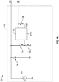
FIG. 1 is a schematic of a power converter having a power supply and a switch; -
FIG. 2 is a schematic of a power converter output voltage associated with a load; -
FIG. 3 is a schematic of a switched snubber circuit associated with a power converter; -
FIG. 4 is a schematic of a low dropout snubber circuit associated with a power converter; and -
FIG. 5 is a graph of an output voltage of a power converter having snubber circuitry. - A detailed description of one or more embodiments of the disclosed apparatus and method are presented herein by way of exemplification and not limitation with reference to the Figures.
- Switched-mode power supplies may include a voltage source and a converter coil (or coils) configured to output the desired voltage based on a switching frequency of a switch associated with the converter coil. The switch may experience stress from voltage transients associated with current flow disruptions. As such, a snubber circuit may be implemented to reduce the transients.
- Referring to
FIG. 1 , apower converter 100 is shown. Thepower converter 100 includespower conversion circuitry 110. This can formed as a single coil or, as illustrated, as a transformer (119) that includes aprimary side 112, asecondary side 114. Regardless of the implementation, thepower conversion circuitry 110 includes a switchingportion 113 that is connected to thepower conversion circuitry 110 and to apower source 104. In one embodiment, thepower source 104 provides DC power and may be a battery. The switchingportion 113 may include DC-link capacitors 106. The DC-link capacitors 106 may reduce fluctuations in voltage provided to thepower conversion circuitry 110 by thepower source 104. The switchingportion 113 may include aswitch 102 or oscillator. Theswitch 102 may be associated with or operated according to a predetermined oscillation frequency. - The
switch 102 may open and close based on associatedresistors 108 or be otherwise driven by a gate driver. As such, theswitch 102 in the closed position may allow current flow from the inductor to ground, and theswitch 102 in the open position may inhibit or reduce such current flow though the inductor. Theswitch 102 may be any type of switching mechanism, including transistors or integrated circuits. Theswitch 102 can be connected between thepower source 104 and aconverter coil 116 or first power conversion winding or may connected between theconverter coil 116 and a reference or ground as illustrated inFIG. 1 . - The
converter coil 116 may be any type of inductor or coil. Theconverter coil 116 may be standalone and connected directly to aconverter load 124 or associated with any type oftransformer 119 andsecondary side 114 to provide voltage toconverter output 125. As illustrated, thesecondary side 114 includes asecondary side coil 118 or second power conversion winding, aconverter diode 120 and a powerconverter output capacitor 122 to properly converter thepower source 104 to the powerconversion circuitry output 125 that is a voltage associated with theconverter load 124 ofpower conversion circuitry 110. A winding ratio of theconverter coil 116 to thesecondary side coil 118 may be 9:4. The configuration may include ratios that are either a step-up or a step-down. Theconverter coil 116 and thesecondary side coil 118 may formpower conversion transformer 119. Theswitch 102 may be configured to control current flowing through theconverter coil 116 such that theoutput 125 is a voltage as desired. - As such, as the
switch 102 is turned on for the first time, current flows from thepower source 104 through theconverter coil 116 and at least one of theresistors 108 to ground. Theswitch 102 may be associated with or operated according to a predetermined oscillation frequency or actuation frequency that is determined by the ratio of R3. It should be appreciated that theswitch 102 may be any type of switching device including transistors. The oscillation frequency may be equal or greater than a resonant frequency of thesnubber capacitor 140 and the parallelsnubber circuitry coil 136. The oscillation frequency may be slightly greater than the resonant frequency of thesnubber capacitor 140 and the parallelsnubber circuitry coil 136. - The
power converter 100 may includeparallel snubber circuitry 130, including parallelsnubber circuitry transformer 149, parallel snubber circuitry output side 134, andresonant circuitry 132 connected in parallel with theconverter coil 116. Theresonant circuitry 132 may include a parallelsnubber circuitry coil 136 or first parallel coil connected in series or pseudo series withsnubber capacitor 140. Thesnubber capacitor 140 may have a capacitance of five microfarads. That is, the parallelsnubber circuitry coil 136 is connected toconverter coil 116 such that respective terminal voltages across are similar. Further, the parallelsnubber circuitry coil 136 and thesnubber capacitor 140 form a series resonant system having a resonant frequency according to Equation 1.
- The inductance of the parallel
snubber circuitry coil 136 may be 10 microhenries. Thesnubber capacitor 140 peak voltage may be determined as Equation 2.
switch 102, and n 1 is the transformation ratio of thetransformer 119 and V out1 is therespective output 125. - The parallel snubber circuitry output side 134 includes a second
parallel coil 144 associated with the parallelsnubber circuitry coil 136 to form parallelsnubber circuitry transformer 149. It should be appreciated that any type of resonant system may be used including those not associated with transformers. The secondparallel coil 144 may be associated with other parallel snubber circuitry output side 134 components including parallel snubbercircuitry output diode 148,output capacitor 131 and may be connectable to parallel snubber circuitry load 133. The parallel snubber circuitry output side 134 may include a parallelsnubber circuitry output 145 having a voltage defined by theparallel snubber circuitry 130. The parallelsnubber circuitry coil 136 may be a first portion or first winding portion of a bifilar winding associated with the second primarybifilar winding portion 138. The parallelsnubber circuitry coil 136 may be a first portion of a bifilar winding associated with the secondbifilar winding portion 138 may have a combined inductance of 10 microhenries. The secondparallel coil 144 may be a first portion of a bifilar winding associated with a second secondarybifilar winding portion 146. - As such, as the
switch 102 is turned off for the first time, current may flow through the convertersecondary side 114 withconverter output 125 as a voltage. Current will additionally flow through thesnubber capacitor 140 through the parallelsnubber circuitry coil 136 andparallel snubber diode 142 to theconverter coil 116. - The
parallel snubber diode 142 may be any type of diode, including a Schottky type. Theparallel snubber diode 142 may be disposed on conductive path 143 between theconverter coil 116 and the parallelsnubber circuitry coil 136. Theparallel snubber diode 142 may be biased to enable less restrictive current flow from the parallelsnubber circuitry coil 136 to theconverter coil 116 than from theconverter coil 116 to the parallelsnubber circuitry coil 136. - The parallel
snubber circuitry coil 136 andsnubber capacitor 140 may be chosen such that they operate in a series resonant mode that achieves less impedance during a freewheeling period. That is, the switching frequency ofswitch 102 may be chosen to be equal or faster, possibly slightly faster, than the resonant frequency as defined in Equation 1 with respect to the parallelsnubber circuitry coil 136 andsnubber capacitor 140. As an example, the parallelsnubber circuitry coil 136 may an inductance of ten microhenries. Thesnubber capacitor 140 may have a capacitance of five microfarads. - The
power converter 100 may includeseries snubber circuitry 150, including seriessnubber circuitry transformer 179, series snubbercircuitry input side 152, and series snubbercircuitry output side 154. The series snubbercircuitry input side 152 includes a series snubbercircuitry input coil 156, series inductor, or first series snubber winding in series with thesnubber capacitor 140 andseries snubber diode 158. Thesnubber capacitor 140 and the series snubbercircuitry input coil 156 form an LC snubber and are connected with theconverter coil 116 in series or pseudo series such that current flows from the series snubbercircuitry input coil 156 throughseries snubber diode 158 and the series associatedsnubber capacitor 140 through theswitch 102. It should be appreciated that theparallel snubber circuitry 130 and theseries snubber circuitry 150 may sharesnubber capacitor 140 to provide the necessary snubbing capabilities. As such, thesnubber capacitor 140 may be configured in such a way as to provide dual purposed capacitance to the resonant circuits of the parallel snubber circuitry and the series snubber circuitry. - The series snubber
circuitry output side 154 associated with seriessnubber circuitry transformer 179 may include aseries output coil 160, second series snubber winding, or series snubber secondary winding. Seriessnubber circuitry transformer 179 may be a flyback transformer. It should be appreciated that any converter or flyback converter shown may be configured as a forward converter (not shown). It should be appreciated that thetransformer 179 may be replaced by any other type of switched-mode power supply and that a flyback, as shown, may be implemented in a variety of ways. Further, the series snubbercircuitry output side 154 may include aseries snubber diode 162 and a series snubbercircuitry output capacitor 164 associated with seriessnubber circuitry output 165 as a voltage and seriessnubber circuitry load 166. - Referring to
FIG. 2 , thepower converter 100 is shown havingpower source 104 and switch 102 in a schematic diagram. Theswitch 102 may be driven or operated by a gate driver and a controller. As shown, thepower conversion circuitry 110,parallel snubber circuitry 130, andseries snubber circuitry 150 are shown. As should be appreciated, each of thecircuitries - The
power conversion circuitry 110,parallel snubber circuitry 130, andseries snubber circuitry 150 are associated withoutputs converter output 125 is a voltage produced by thepower conversion circuitry 110, theparallel snubber output 145 is a voltage produced by theparallel snubber circuitry 130 and theseries snubber output 165 is a voltage produced by theseries snubber circuitry 150. As such, theoutputs voltage output 185 of the power converter having a predetermined voltage. Additionally, any of theoutputs voltage output 185. That is, reverse polarity may be used on any of the diodes associated with thepower conversion circuitry 110,parallel snubber circuitry 130, andseries snubber circuitry 150 to create the desired output voltage. Thepower conversion circuitry 110,parallel snubber circuitry 130, andseries snubber circuitry 150 may further be associated in parallel. For example, the power conversion circuitry polarity and the parallel snubber circuitry polarity may be the same and opposite of the series snubber circuitry polarity to reduce thevoltage output 185 by the seriessnubber circuitry output 165. - Referring to
FIG. 3 ,series snubber circuitry 250 is shown. Thepower converter 100 may includeseries snubber circuitry 250, including seriessnubber circuitry transformer 279, series snubbercircuitry input side 252, and series snubbercircuitry output side 254. The series snubbercircuitry input side 252 may include a series snubbercircuitry input coil 256 in series with the snubber capacitor 140 (not shown) andseries snubber diode 258. Thesnubber capacitor 140 and the series snubbercircuitry input coil 256 form a series resonant snubber and are connected with theconverter coil 116 in series or pseudo series such that current from thepower source 104 flows from the series snubbercircuitry input coil 256 throughseries snubber diode 258 and the series associatedsnubber capacitor 140 through theswitch 102. The current may be controlled bypulsed power supply 236 configured as a gate driver forseries snubber switch 238. - The series snubber
circuitry output side 254 associated withtransformer 279 may include aseries output coil 260. It should be appreciated that thetransformer 279 may be replaced by any other type of switched-mode power supply and that a flyback, as shown, may be implemented in a variety of ways. Further, the series snubbercircuitry output side 254 may include aseries snubber diode 262 and a seriessnubber output capacitor 264 associated with seriessnubber circuitry output 265 as a voltage and series snubbercircuitry output load 266. - Referring to
FIG. 4 ,series snubber circuitry 350 is shown. Theseries snubber circuitry 350 may include a series snubber circuitry lowdropout voltage regulator 372 or another other type of voltage regulator in series with the snubber capacitor 140 (not shown) andseries snubber diode 358 and may be associated withlow dropout capacitor 370. The lowdropout voltage regulator 372 may provideoutput voltage 365 associated withseries snubber output 366. - Referring to
FIG. 5 , agraph 500 is shown. Thegraph 500 includes output voltages associated with thepower conversion circuitry 110, theparallel snubber circuitry 130, and theseries snubber circuitry 150, where theconverter output 125 is a voltage produced by thepower conversion circuitry 110, theparallel snubber output 145 is a voltage produced by theparallel snubber circuitry 130 and theseries snubber output 165 is a voltage produced by theseries snubber circuitry 150. Thepower source 104 may, as one example, be a 30-volt direct current source having associatedoutputs - The term "about" is intended to include the degree of error associated with measurement of the particular quantity based upon the equipment available at the time of filing the application.
- The terminology used herein is for the purpose of describing particular embodiments only and is not intended to be limiting of the present disclosure. As used herein, the singular forms "a", "an" and "the" are intended to include the plural forms as well, unless the context clearly indicates otherwise. It will be further understood that the terms "comprises" and/or "comprising," when used in this specification, specify the presence of stated features, integers, steps, operations, elements, and/or components, but do not preclude the presence or addition of one or more other features, integers, steps, operations, element components, and/or groups thereof.
- While the present disclosure has been described with reference to an exemplary embodiment or embodiments, it will be understood by those skilled in the art that various changes may be made and equivalents may be substituted for elements thereof without departing from the scope of the present disclosure. In addition, many modifications may be made to adapt a particular situation or material to the teachings of the present disclosure without departing from the scope of the invention as defined by the claims. Therefore, it is intended that the present disclosure not be limited to the particular embodiment disclosed as the best mode contemplated for carrying out this present disclosure, but that the invention will include all embodiments falling within the scope of the claims.
Claims (15)
- A power converter comprising:
power conversion circuitry (110) including:a converter coil (116),a power source (104), anda switch (102) connected to the converter coil to control current flowing through the converter coil from the power source, the power conversion circuitry including a converter output connectable to a converter load; andparallel snubber circuitry (130) having resonant circuitry (132) connected in parallel with the converter coil, the resonant circuitry including a parallel snubber circuitry coil (136) and a capacitor (140) connected in series, the parallel snubber circuitry including a parallel snubber output (134) connectable to a parallel snubber circuitry load (133). - The power converter of claim 1, wherein the parallel snubber circuitry coil is a first parallel coil of the parallel snubber circuitry, and further comprising, a second parallel coil (144) associated with the first parallel coil to form a parallel snubber circuitry transformer.
- The power converter of claim 2, wherein the parallel snubber circuitry transformer is configured to supply power to the parallel snubber circuitry load associated with the parallel snubber circuitry transformer.
- The power converter of claim 2 or 3, wherein the parallel snubber circuitry transformer has a winding ratio of 9:4 between the first parallel coil and the second parallel coil.
- The power converter of any preceding claim, further comprising a parallel snubber diode (142) disposed on a conductive path between the converter coil and the parallel snubber circuitry coil and biased to enable less restrictive current flow from the parallel snubber circuitry coil to the converter coil than from the converter coil to the parallel snubber circuitry coil.
- The power converter of any preceding claim, wherein the switch is associated with a predefined oscillation frequency greater than a resonant frequency of the capacitor and the parallel snubber circuitry coil, and optionally wherein the capacitor has a capacitance of five microfarads and the parallel snubber circuitry coil has an inductance of 10 microhenries.
- The power converter of any preceding claim, wherein the parallel snubber circuitry coil is bifilar having a first winding portion and a second winding portion, and optionally wherein the first winding portion and the second winding portion have a combined inductance of 10 microhenries.
- The power converter of any preceding claim, further comprising series snubber circuitry (150) associated with the converter coil including a series inductor disposed in series with the converter coil and the capacitor with respect to the power source, and a series snubber diode (158) disposed between the parallel and the converter coil.
- The power converter of any preceding claim, further comprising series snubber circuitry associated with the converter coil including a low dropout voltage regulator (372) in series with the converter coil with respect to the power source.
- The power converter of any preceding claim, further comprising series snubber circuitry associated with the converter coil including a flyback transformer in series with the converter coil with respect to the power source; and optionally wherein the series snubber circuitry has a series snubber circuitry voltage output with a series snubber circuitry voltage polarity opposite a power conversion circuitry polarity of the power conversion circuitry such that a power converter output voltage of the power converter is less the series snubber circuitry voltage output; and optionally wherein the flyback transformer includes a load side having series snubber circuitry secondary winding, a series snubber circuitry load, and a series snubber diode disposed is biased to enable less restrictive current flow from the series snubber circuitry load to the series snubber circuitry secondary winding than from the series snubber circuitry secondary winding to the series snubber circuitry load.
- The power converter of any preceding claim, further comprising series snubber circuitry having a series snubber circuitry output (254) configured in series with a parallel snubber circuitry output of the parallel snubber circuitry in series with the converter output.
- The power converter of claim 11, wherein the series snubber circuitry includes a series snubber circuitry transformer (279) having a winding ratio of 13:5 between a first series snubber winding and a second series snubber winding; and/or wherein the power conversion circuitry includes a power conversion transformer having a winding ratio of 13:5 between a first power conversion winding and a second power conversion winding.
- The power converter of any preceding claim, further comprising controller circuitry operable to oscillate the switch between an open position and a closed position according to a predetermined output voltage command associated with the power converter.
- A power converter comprising:power conversion circuitry including a converter coil associated with a power supply and a switch configured with a power conversion circuitry output to a converter load associated with the power converter; andparallel snubber circuitry associated with the converter coil having a parallel snubber circuitry coil disposed in parallel with the converter coil with respect to the power supply, a parallel snubber diode disposed between the parallel snubber circuitry coil and the converter coil biased to enable less restrictive current flow from the parallel snubber circuitry coil to the converter coil than from the converter coil to the parallel snubber circuitry coil, and a capacitor disposed between the parallel snubber circuitry coil and the converter coil.
- A power converter as claimed in claim 14, further comprising:
series snubber circuitry having a series snubber circuitry output configured in series with a parallel snubber circuitry output of the parallel snubber circuitry in series with the power conversion circuitry output forming a power converter output voltage having a predetermined voltage.
Applications Claiming Priority (1)
| Application Number | Priority Date | Filing Date | Title |
|---|---|---|---|
| IN201911022516 | 2019-06-06 |
Publications (2)
| Publication Number | Publication Date |
|---|---|
| EP3748830A1 true EP3748830A1 (en) | 2020-12-09 |
| EP3748830B1 EP3748830B1 (en) | 2023-02-22 |
Family
ID=70977851
Family Applications (1)
| Application Number | Title | Priority Date | Filing Date |
|---|---|---|---|
| EP20178330.5A Active EP3748830B1 (en) | 2019-06-06 | 2020-06-04 | Power converter with snubber circuit |
Country Status (2)
| Country | Link |
|---|---|
| US (1) | US10797587B1 (en) |
| EP (1) | EP3748830B1 (en) |
Citations (4)
| Publication number | Priority date | Publication date | Assignee | Title |
|---|---|---|---|---|
| JP2001145346A (en) * | 1999-11-17 | 2001-05-25 | Sharp Corp | Switching power supply snubber circuit |
| US20140085937A1 (en) * | 2012-09-27 | 2014-03-27 | Industrial Technology Research Institute | Dc-dc converter and method of driving the same |
| CN104953841A (en) * | 2014-03-28 | 2015-09-30 | 东林科技股份有限公司 | Power supply conversion device |
| CN207896876U (en) * | 2018-01-26 | 2018-09-21 | 同方泰德国际科技(北京)有限公司 | A kind of energy feedback type snubber circuit applied to Switching Power Supply |
Family Cites Families (11)
| Publication number | Priority date | Publication date | Assignee | Title |
|---|---|---|---|---|
| US3628047A (en) * | 1970-04-06 | 1971-12-14 | Trw Inc | Nondissipative power loss suppression circuit for transistor controlled power converters |
| US4675796A (en) * | 1985-05-17 | 1987-06-23 | Veeco Instruments, Inc. | High switching frequency converter auxiliary magnetic winding and snubber circuit |
| JPH04127831A (en) * | 1990-09-18 | 1992-04-28 | Mitsubishi Electric Corp | Snubber circuit |
| US5508903A (en) | 1995-04-21 | 1996-04-16 | Alexndrov; Felix | Interleaved DC to DC flyback converters with reduced current and voltage stresses |
| US20010019490A1 (en) * | 1997-12-03 | 2001-09-06 | Fuji Electric Co., Ltd. | Switching power supply |
| US6473318B1 (en) * | 2000-11-20 | 2002-10-29 | Koninklijke Philips Electronics N.V. | Leakage energy recovering system and method for flyback converter |
| US6477064B1 (en) | 2001-10-10 | 2002-11-05 | Koninklijke Philips Electronics N.V. | High efficiency DC-DC power converter with turn-off snubber |
| US20070047275A1 (en) | 2005-08-30 | 2007-03-01 | Hesterman Bryce L | Bipolar power supply with lossless snubber |
| EP2814155A1 (en) * | 2013-06-11 | 2014-12-17 | ABB Research Ltd. | LC snubber circuit |
| US20150085534A1 (en) | 2013-09-20 | 2015-03-26 | Alexander ABRAMOVITZ | Regenerative and ramping acceleration (rara) snubbers for isolated and tapped-inductor converters |
| US9780676B2 (en) | 2016-02-22 | 2017-10-03 | Infineon Technologies Austria Ag | Power converter with a snubber circuit |
-
2019
- 2019-08-16 US US16/542,990 patent/US10797587B1/en active Active
-
2020
- 2020-06-04 EP EP20178330.5A patent/EP3748830B1/en active Active
Patent Citations (4)
| Publication number | Priority date | Publication date | Assignee | Title |
|---|---|---|---|---|
| JP2001145346A (en) * | 1999-11-17 | 2001-05-25 | Sharp Corp | Switching power supply snubber circuit |
| US20140085937A1 (en) * | 2012-09-27 | 2014-03-27 | Industrial Technology Research Institute | Dc-dc converter and method of driving the same |
| CN104953841A (en) * | 2014-03-28 | 2015-09-30 | 东林科技股份有限公司 | Power supply conversion device |
| CN207896876U (en) * | 2018-01-26 | 2018-09-21 | 同方泰德国际科技(北京)有限公司 | A kind of energy feedback type snubber circuit applied to Switching Power Supply |
Also Published As
| Publication number | Publication date |
|---|---|
| EP3748830B1 (en) | 2023-02-22 |
| US10797587B1 (en) | 2020-10-06 |
Similar Documents
| Publication | Publication Date | Title |
|---|---|---|
| US10263528B2 (en) | Resonant converter with adaptive switching frequency and the method thereof | |
| TWI404317B (en) | Dual-polarity dual-output synchronous boost converters and method for operating the same | |
| US8441290B2 (en) | Method and apparatus for simplifying the control of a switch | |
| US9564820B2 (en) | Methods and systems for control of DC-DC converters | |
| EP3683942A1 (en) | Drive circuit | |
| EP2526615B1 (en) | Power conversion with zero voltage switching | |
| EP1753118A2 (en) | Multi-voltage power supply | |
| US20150188405A1 (en) | High efficiency resonant switched capacitor converter with continuous conversion ratio | |
| US10256733B2 (en) | Tapped winding flyback converter for multiple output voltages | |
| US20200336074A1 (en) | Flyback Power Converters Including Adaptive Clamp Circuits For Adjusting Resonant Frequencies | |
| EP3736956A1 (en) | Drive scheme for weakly coupled coils | |
| US8767423B2 (en) | Method and apparatus for varying current limit to limit an output power of a power supply | |
| DE102009045052A1 (en) | Providing a supply voltage for a drive circuit of a semiconductor switching element | |
| US9819277B2 (en) | Isolated buck converter, switched mode power supply, and method of transferring digital data from a primary side to an isolated secondary side of an isolated buck converter | |
| CN111224551B (en) | Power Converters | |
| US20170244330A1 (en) | Power Converter with a Snubber Circuit | |
| EP2045903A2 (en) | DC-DC converter | |
| JPH05252733A (en) | Power supply that generates DC output voltage | |
| JP6908849B2 (en) | Synchronous rectifier circuit and switching power supply | |
| EP3748830B1 (en) | Power converter with snubber circuit | |
| EP4191857B1 (en) | Adaptive controller for a voltage converter | |
| US10644688B2 (en) | Biasing circuit for switch | |
| EP3499702A1 (en) | Hold-up capacitor charging using fly-back power supply | |
| US8324872B2 (en) | Voltage regulator with coupled inductors having high coefficient of coupling | |
| US12445059B2 (en) | Synchronous switch driver with switched filter |
Legal Events
| Date | Code | Title | Description |
|---|---|---|---|
| PUAI | Public reference made under article 153(3) epc to a published international application that has entered the european phase |
Free format text: ORIGINAL CODE: 0009012 |
|
| STAA | Information on the status of an ep patent application or granted ep patent |
Free format text: STATUS: THE APPLICATION HAS BEEN PUBLISHED |
|
| AK | Designated contracting states |
Kind code of ref document: A1 Designated state(s): AL AT BE BG CH CY CZ DE DK EE ES FI FR GB GR HR HU IE IS IT LI LT LU LV MC MK MT NL NO PL PT RO RS SE SI SK SM TR |
|
| AX | Request for extension of the european patent |
Extension state: BA ME |
|
| STAA | Information on the status of an ep patent application or granted ep patent |
Free format text: STATUS: REQUEST FOR EXAMINATION WAS MADE |
|
| 17P | Request for examination filed |
Effective date: 20210609 |
|
| RBV | Designated contracting states (corrected) |
Designated state(s): AL AT BE BG CH CY CZ DE DK EE ES FI FR GB GR HR HU IE IS IT LI LT LU LV MC MK MT NL NO PL PT RO RS SE SI SK SM TR |
|
| STAA | Information on the status of an ep patent application or granted ep patent |
Free format text: STATUS: EXAMINATION IS IN PROGRESS |
|
| 17Q | First examination report despatched |
Effective date: 20210720 |
|
| GRAP | Despatch of communication of intention to grant a patent |
Free format text: ORIGINAL CODE: EPIDOSNIGR1 |
|
| STAA | Information on the status of an ep patent application or granted ep patent |
Free format text: STATUS: GRANT OF PATENT IS INTENDED |
|
| INTG | Intention to grant announced |
Effective date: 20220914 |
|
| GRAS | Grant fee paid |
Free format text: ORIGINAL CODE: EPIDOSNIGR3 |
|
| GRAA | (expected) grant |
Free format text: ORIGINAL CODE: 0009210 |
|
| STAA | Information on the status of an ep patent application or granted ep patent |
Free format text: STATUS: THE PATENT HAS BEEN GRANTED |
|
| AK | Designated contracting states |
Kind code of ref document: B1 Designated state(s): AL AT BE BG CH CY CZ DE DK EE ES FI FR GB GR HR HU IE IS IT LI LT LU LV MC MK MT NL NO PL PT RO RS SE SI SK SM TR |
|
| REG | Reference to a national code |
Ref country code: GB Ref legal event code: FG4D |
|
| REG | Reference to a national code |
Ref country code: CH Ref legal event code: EP |
|
| REG | Reference to a national code |
Ref country code: DE Ref legal event code: R096 Ref document number: 602020008210 Country of ref document: DE |
|
| REG | Reference to a national code |
Ref country code: AT Ref legal event code: REF Ref document number: 1550145 Country of ref document: AT Kind code of ref document: T Effective date: 20230315 Ref country code: IE Ref legal event code: FG4D |
|
| REG | Reference to a national code |
Ref country code: LT Ref legal event code: MG9D |
|
| REG | Reference to a national code |
Ref country code: NL Ref legal event code: MP Effective date: 20230222 |
|
| P01 | Opt-out of the competence of the unified patent court (upc) registered |
Effective date: 20230603 |
|
| REG | Reference to a national code |
Ref country code: AT Ref legal event code: MK05 Ref document number: 1550145 Country of ref document: AT Kind code of ref document: T Effective date: 20230222 |
|
| PG25 | Lapsed in a contracting state [announced via postgrant information from national office to epo] |
Ref country code: RS Free format text: LAPSE BECAUSE OF FAILURE TO SUBMIT A TRANSLATION OF THE DESCRIPTION OR TO PAY THE FEE WITHIN THE PRESCRIBED TIME-LIMIT Effective date: 20230222 Ref country code: PT Free format text: LAPSE BECAUSE OF FAILURE TO SUBMIT A TRANSLATION OF THE DESCRIPTION OR TO PAY THE FEE WITHIN THE PRESCRIBED TIME-LIMIT Effective date: 20230622 Ref country code: NO Free format text: LAPSE BECAUSE OF FAILURE TO SUBMIT A TRANSLATION OF THE DESCRIPTION OR TO PAY THE FEE WITHIN THE PRESCRIBED TIME-LIMIT Effective date: 20230522 Ref country code: NL Free format text: LAPSE BECAUSE OF FAILURE TO SUBMIT A TRANSLATION OF THE DESCRIPTION OR TO PAY THE FEE WITHIN THE PRESCRIBED TIME-LIMIT Effective date: 20230222 Ref country code: LV Free format text: LAPSE BECAUSE OF FAILURE TO SUBMIT A TRANSLATION OF THE DESCRIPTION OR TO PAY THE FEE WITHIN THE PRESCRIBED TIME-LIMIT Effective date: 20230222 Ref country code: LT Free format text: LAPSE BECAUSE OF FAILURE TO SUBMIT A TRANSLATION OF THE DESCRIPTION OR TO PAY THE FEE WITHIN THE PRESCRIBED TIME-LIMIT Effective date: 20230222 Ref country code: HR Free format text: LAPSE BECAUSE OF FAILURE TO SUBMIT A TRANSLATION OF THE DESCRIPTION OR TO PAY THE FEE WITHIN THE PRESCRIBED TIME-LIMIT Effective date: 20230222 Ref country code: ES Free format text: LAPSE BECAUSE OF FAILURE TO SUBMIT A TRANSLATION OF THE DESCRIPTION OR TO PAY THE FEE WITHIN THE PRESCRIBED TIME-LIMIT Effective date: 20230222 Ref country code: AT Free format text: LAPSE BECAUSE OF FAILURE TO SUBMIT A TRANSLATION OF THE DESCRIPTION OR TO PAY THE FEE WITHIN THE PRESCRIBED TIME-LIMIT Effective date: 20230222 |
|
| PG25 | Lapsed in a contracting state [announced via postgrant information from national office to epo] |
Ref country code: SE Free format text: LAPSE BECAUSE OF FAILURE TO SUBMIT A TRANSLATION OF THE DESCRIPTION OR TO PAY THE FEE WITHIN THE PRESCRIBED TIME-LIMIT Effective date: 20230222 Ref country code: PL Free format text: LAPSE BECAUSE OF FAILURE TO SUBMIT A TRANSLATION OF THE DESCRIPTION OR TO PAY THE FEE WITHIN THE PRESCRIBED TIME-LIMIT Effective date: 20230222 Ref country code: IS Free format text: LAPSE BECAUSE OF FAILURE TO SUBMIT A TRANSLATION OF THE DESCRIPTION OR TO PAY THE FEE WITHIN THE PRESCRIBED TIME-LIMIT Effective date: 20230622 Ref country code: GR Free format text: LAPSE BECAUSE OF FAILURE TO SUBMIT A TRANSLATION OF THE DESCRIPTION OR TO PAY THE FEE WITHIN THE PRESCRIBED TIME-LIMIT Effective date: 20230523 Ref country code: FI Free format text: LAPSE BECAUSE OF FAILURE TO SUBMIT A TRANSLATION OF THE DESCRIPTION OR TO PAY THE FEE WITHIN THE PRESCRIBED TIME-LIMIT Effective date: 20230222 |
|
| PG25 | Lapsed in a contracting state [announced via postgrant information from national office to epo] |
Ref country code: SM Free format text: LAPSE BECAUSE OF FAILURE TO SUBMIT A TRANSLATION OF THE DESCRIPTION OR TO PAY THE FEE WITHIN THE PRESCRIBED TIME-LIMIT Effective date: 20230222 Ref country code: RO Free format text: LAPSE BECAUSE OF FAILURE TO SUBMIT A TRANSLATION OF THE DESCRIPTION OR TO PAY THE FEE WITHIN THE PRESCRIBED TIME-LIMIT Effective date: 20230222 Ref country code: EE Free format text: LAPSE BECAUSE OF FAILURE TO SUBMIT A TRANSLATION OF THE DESCRIPTION OR TO PAY THE FEE WITHIN THE PRESCRIBED TIME-LIMIT Effective date: 20230222 Ref country code: DK Free format text: LAPSE BECAUSE OF FAILURE TO SUBMIT A TRANSLATION OF THE DESCRIPTION OR TO PAY THE FEE WITHIN THE PRESCRIBED TIME-LIMIT Effective date: 20230222 Ref country code: CZ Free format text: LAPSE BECAUSE OF FAILURE TO SUBMIT A TRANSLATION OF THE DESCRIPTION OR TO PAY THE FEE WITHIN THE PRESCRIBED TIME-LIMIT Effective date: 20230222 |
|
| REG | Reference to a national code |
Ref country code: DE Ref legal event code: R097 Ref document number: 602020008210 Country of ref document: DE |
|
| PG25 | Lapsed in a contracting state [announced via postgrant information from national office to epo] |
Ref country code: SK Free format text: LAPSE BECAUSE OF FAILURE TO SUBMIT A TRANSLATION OF THE DESCRIPTION OR TO PAY THE FEE WITHIN THE PRESCRIBED TIME-LIMIT Effective date: 20230222 |
|
| PLBE | No opposition filed within time limit |
Free format text: ORIGINAL CODE: 0009261 |
|
| STAA | Information on the status of an ep patent application or granted ep patent |
Free format text: STATUS: NO OPPOSITION FILED WITHIN TIME LIMIT |
|
| PG25 | Lapsed in a contracting state [announced via postgrant information from national office to epo] |
Ref country code: MC Free format text: LAPSE BECAUSE OF FAILURE TO SUBMIT A TRANSLATION OF THE DESCRIPTION OR TO PAY THE FEE WITHIN THE PRESCRIBED TIME-LIMIT Effective date: 20230222 |
|
| 26N | No opposition filed |
Effective date: 20231123 |
|
| PG25 | Lapsed in a contracting state [announced via postgrant information from national office to epo] |
Ref country code: SI Free format text: LAPSE BECAUSE OF FAILURE TO SUBMIT A TRANSLATION OF THE DESCRIPTION OR TO PAY THE FEE WITHIN THE PRESCRIBED TIME-LIMIT Effective date: 20230222 Ref country code: MC Free format text: LAPSE BECAUSE OF FAILURE TO SUBMIT A TRANSLATION OF THE DESCRIPTION OR TO PAY THE FEE WITHIN THE PRESCRIBED TIME-LIMIT Effective date: 20230222 |
|
| REG | Reference to a national code |
Ref country code: CH Ref legal event code: PL |
|
| REG | Reference to a national code |
Ref country code: BE Ref legal event code: MM Effective date: 20230630 |
|
| PG25 | Lapsed in a contracting state [announced via postgrant information from national office to epo] |
Ref country code: LU Free format text: LAPSE BECAUSE OF NON-PAYMENT OF DUE FEES Effective date: 20230604 |
|
| REG | Reference to a national code |
Ref country code: IE Ref legal event code: MM4A |
|
| PG25 | Lapsed in a contracting state [announced via postgrant information from national office to epo] |
Ref country code: LU Free format text: LAPSE BECAUSE OF NON-PAYMENT OF DUE FEES Effective date: 20230604 |
|
| PG25 | Lapsed in a contracting state [announced via postgrant information from national office to epo] |
Ref country code: IE Free format text: LAPSE BECAUSE OF NON-PAYMENT OF DUE FEES Effective date: 20230604 |
|
| PG25 | Lapsed in a contracting state [announced via postgrant information from national office to epo] |
Ref country code: IE Free format text: LAPSE BECAUSE OF NON-PAYMENT OF DUE FEES Effective date: 20230604 Ref country code: CH Free format text: LAPSE BECAUSE OF NON-PAYMENT OF DUE FEES Effective date: 20230630 |
|
| PG25 | Lapsed in a contracting state [announced via postgrant information from national office to epo] |
Ref country code: IT Free format text: LAPSE BECAUSE OF FAILURE TO SUBMIT A TRANSLATION OF THE DESCRIPTION OR TO PAY THE FEE WITHIN THE PRESCRIBED TIME-LIMIT Effective date: 20230222 Ref country code: BE Free format text: LAPSE BECAUSE OF NON-PAYMENT OF DUE FEES Effective date: 20230630 |
|
| PG25 | Lapsed in a contracting state [announced via postgrant information from national office to epo] |
Ref country code: BG Free format text: LAPSE BECAUSE OF FAILURE TO SUBMIT A TRANSLATION OF THE DESCRIPTION OR TO PAY THE FEE WITHIN THE PRESCRIBED TIME-LIMIT Effective date: 20230222 |
|
| PG25 | Lapsed in a contracting state [announced via postgrant information from national office to epo] |
Ref country code: BG Free format text: LAPSE BECAUSE OF FAILURE TO SUBMIT A TRANSLATION OF THE DESCRIPTION OR TO PAY THE FEE WITHIN THE PRESCRIBED TIME-LIMIT Effective date: 20230222 |
|
| PGFP | Annual fee paid to national office [announced via postgrant information from national office to epo] |
Ref country code: DE Payment date: 20250520 Year of fee payment: 6 |
|
| PGFP | Annual fee paid to national office [announced via postgrant information from national office to epo] |
Ref country code: GB Payment date: 20250520 Year of fee payment: 6 |
|
| PGFP | Annual fee paid to national office [announced via postgrant information from national office to epo] |
Ref country code: FR Payment date: 20250521 Year of fee payment: 6 |
|
| PG25 | Lapsed in a contracting state [announced via postgrant information from national office to epo] |
Ref country code: CY Free format text: LAPSE BECAUSE OF FAILURE TO SUBMIT A TRANSLATION OF THE DESCRIPTION OR TO PAY THE FEE WITHIN THE PRESCRIBED TIME-LIMIT; INVALID AB INITIO Effective date: 20200604 |
|
| PG25 | Lapsed in a contracting state [announced via postgrant information from national office to epo] |
Ref country code: HU Free format text: LAPSE BECAUSE OF FAILURE TO SUBMIT A TRANSLATION OF THE DESCRIPTION OR TO PAY THE FEE WITHIN THE PRESCRIBED TIME-LIMIT; INVALID AB INITIO Effective date: 20200604 |
|
| PG25 | Lapsed in a contracting state [announced via postgrant information from national office to epo] |
Ref country code: TR Free format text: LAPSE BECAUSE OF FAILURE TO SUBMIT A TRANSLATION OF THE DESCRIPTION OR TO PAY THE FEE WITHIN THE PRESCRIBED TIME-LIMIT Effective date: 20230222 |