EP3748578B1 - Automatic visual detection of defects in images of via holes - Google Patents
Automatic visual detection of defects in images of via holes Download PDFInfo
- Publication number
- EP3748578B1 EP3748578B1 EP20171769.1A EP20171769A EP3748578B1 EP 3748578 B1 EP3748578 B1 EP 3748578B1 EP 20171769 A EP20171769 A EP 20171769A EP 3748578 B1 EP3748578 B1 EP 3748578B1
- Authority
- EP
- European Patent Office
- Prior art keywords
- cluster
- pixel value
- average pixel
- view image
- obtaining
- Prior art date
- Legal status (The legal status is an assumption and is not a legal conclusion. Google has not performed a legal analysis and makes no representation as to the accuracy of the status listed.)
- Active
Links
Images



Classifications
-
- G—PHYSICS
- G06—COMPUTING OR CALCULATING; COUNTING
- G06T—IMAGE DATA PROCESSING OR GENERATION, IN GENERAL
- G06T7/00—Image analysis
- G06T7/10—Segmentation; Edge detection
- G06T7/13—Edge detection
-
- G—PHYSICS
- G06—COMPUTING OR CALCULATING; COUNTING
- G06T—IMAGE DATA PROCESSING OR GENERATION, IN GENERAL
- G06T7/00—Image analysis
- G06T7/0002—Inspection of images, e.g. flaw detection
- G06T7/0004—Industrial image inspection
- G06T7/001—Industrial image inspection using an image reference approach
-
- G—PHYSICS
- G06—COMPUTING OR CALCULATING; COUNTING
- G06T—IMAGE DATA PROCESSING OR GENERATION, IN GENERAL
- G06T7/00—Image analysis
- G06T7/0002—Inspection of images, e.g. flaw detection
- G06T7/0004—Industrial image inspection
-
- G—PHYSICS
- G06—COMPUTING OR CALCULATING; COUNTING
- G06T—IMAGE DATA PROCESSING OR GENERATION, IN GENERAL
- G06T7/00—Image analysis
- G06T7/10—Segmentation; Edge detection
- G06T7/136—Segmentation; Edge detection involving thresholding
-
- G—PHYSICS
- G06—COMPUTING OR CALCULATING; COUNTING
- G06T—IMAGE DATA PROCESSING OR GENERATION, IN GENERAL
- G06T7/00—Image analysis
- G06T7/60—Analysis of geometric attributes
-
- H—ELECTRICITY
- H10—SEMICONDUCTOR DEVICES; ELECTRIC SOLID-STATE DEVICES NOT OTHERWISE PROVIDED FOR
- H10P—GENERIC PROCESSES OR APPARATUS FOR THE MANUFACTURE OR TREATMENT OF DEVICES COVERED BY CLASS H10
- H10P74/00—Testing or measuring during manufacture or treatment of wafers, substrates or devices
- H10P74/20—Testing or measuring during manufacture or treatment of wafers, substrates or devices characterised by the properties tested or measured, e.g. structural or electrical properties
- H10P74/203—Structural properties, e.g. testing or measuring thicknesses, line widths, warpage, bond strengths or physical defects
-
- G—PHYSICS
- G01—MEASURING; TESTING
- G01N—INVESTIGATING OR ANALYSING MATERIALS BY DETERMINING THEIR CHEMICAL OR PHYSICAL PROPERTIES
- G01N23/00—Investigating or analysing materials by the use of wave or particle radiation, e.g. X-rays or neutrons, not covered by groups G01N3/00 – G01N17/00, G01N21/00 or G01N22/00
- G01N23/22—Investigating or analysing materials by the use of wave or particle radiation, e.g. X-rays or neutrons, not covered by groups G01N3/00 – G01N17/00, G01N21/00 or G01N22/00 by measuring secondary emission from the material
- G01N23/225—Investigating or analysing materials by the use of wave or particle radiation, e.g. X-rays or neutrons, not covered by groups G01N3/00 – G01N17/00, G01N21/00 or G01N22/00 by measuring secondary emission from the material using electron or ion
- G01N23/2251—Investigating or analysing materials by the use of wave or particle radiation, e.g. X-rays or neutrons, not covered by groups G01N3/00 – G01N17/00, G01N21/00 or G01N22/00 by measuring secondary emission from the material using electron or ion using incident electron beams, e.g. scanning electron microscopy [SEM]
-
- G—PHYSICS
- G06—COMPUTING OR CALCULATING; COUNTING
- G06T—IMAGE DATA PROCESSING OR GENERATION, IN GENERAL
- G06T2207/00—Indexing scheme for image analysis or image enhancement
- G06T2207/30—Subject of image; Context of image processing
- G06T2207/30108—Industrial image inspection
- G06T2207/30148—Semiconductor; IC; Wafer
-
- H—ELECTRICITY
- H01—ELECTRIC ELEMENTS
- H01J—ELECTRIC DISCHARGE TUBES OR DISCHARGE LAMPS
- H01J2237/00—Discharge tubes exposing object to beam, e.g. for analysis treatment, etching, imaging
- H01J2237/22—Treatment of data
- H01J2237/221—Image processing
-
- H—ELECTRICITY
- H01—ELECTRIC ELEMENTS
- H01J—ELECTRIC DISCHARGE TUBES OR DISCHARGE LAMPS
- H01J2237/00—Discharge tubes exposing object to beam, e.g. for analysis treatment, etching, imaging
- H01J2237/26—Electron or ion microscopes
- H01J2237/28—Scanning microscopes
- H01J2237/2809—Scanning microscopes characterised by the imaging problems involved
- H01J2237/281—Bottom of trenches or holes
-
- H—ELECTRICITY
- H01—ELECTRIC ELEMENTS
- H01J—ELECTRIC DISCHARGE TUBES OR DISCHARGE LAMPS
- H01J2237/00—Discharge tubes exposing object to beam, e.g. for analysis treatment, etching, imaging
- H01J2237/26—Electron or ion microscopes
- H01J2237/28—Scanning microscopes
- H01J2237/2813—Scanning microscopes characterised by the application
- H01J2237/2817—Pattern inspection
-
- H—ELECTRICITY
- H10—SEMICONDUCTOR DEVICES; ELECTRIC SOLID-STATE DEVICES NOT OTHERWISE PROVIDED FOR
- H10B—ELECTRONIC MEMORY DEVICES
- H10B43/00—EEPROM devices comprising charge-trapping gate insulators
- H10B43/10—EEPROM devices comprising charge-trapping gate insulators characterised by the top-view layout
-
- H—ELECTRICITY
- H10—SEMICONDUCTOR DEVICES; ELECTRIC SOLID-STATE DEVICES NOT OTHERWISE PROVIDED FOR
- H10B—ELECTRONIC MEMORY DEVICES
- H10B43/00—EEPROM devices comprising charge-trapping gate insulators
- H10B43/20—EEPROM devices comprising charge-trapping gate insulators characterised by three-dimensional [3D] arrangements, e.g. with cells on different height levels
- H10B43/23—EEPROM devices comprising charge-trapping gate insulators characterised by three-dimensional [3D] arrangements, e.g. with cells on different height levels with source and drain on different levels, e.g. with sloping channels
- H10B43/27—EEPROM devices comprising charge-trapping gate insulators characterised by three-dimensional [3D] arrangements, e.g. with cells on different height levels with source and drain on different levels, e.g. with sloping channels the channels comprising vertical portions, e.g. U-shaped channels
Definitions
- the disclosure relates in general to a detecting method and a detecting apparatus using the same, and more particularly to an automatic detecting method and an automatic detecting apparatus using the same.
- metal lines located at different layer may be electrically connected through a via hole filled with a conductive material.
- the via hole may be formed by etching an insulation layer. However, if a residue is remained in an etched via hole, the conductivity may be greatly reduced. Therefore, the researchers try to develop an automatic detecting apparatus for detecting the etched via hole.
- a method of inspecting patterns formed the manufacturing of semiconductor devices or the like which includes producing an image of the patterns, producing a boundary image including a plurality of boundary patterns corresponding to first and second boundary of each of the patterns, combing the pattern image and the boundary image to produce an overlapping image including overlapping patterns in which the patterns fill regions between the boundary patterns, and binarizing the overlapping image to produce a binary image including binary patterns corresponding to the overlapping patterns.
- the disclosure is directed to an automatic detecting method as defined in claim 8 and an automatic detecting apparatus using the same as defined in claim 1.
- residues in an etched via hole can be automatically detected without any human power. Therefore, 100% inspection for a plurality of etched via holes is possible.
- Individual embodiments of the invention are the subject matter of the dependent claims.
- an automatic detecting apparatus for detecting an etched via hole.
- the automatic detecting apparatus includes an inputting unit, a dividing unit, a contouring unit, a range analyzing unit, a boundary analyzing unit, an edge detecting unit, an expanding unit and an overlapping unit.
- the inputting unit is used for inputting a top-view image of the etched via hole.
- the dividing unit is used for dividing the top-view image into a first cluster, a second cluster, a third cluster and a fourth cluster via a clustering algorithm.
- the contouring unit is used for obtaining a contour according to the first cluster.
- a first average pixel value of the first cluster is larger than a second average pixel value of the second cluster, a third average pixel value of the third cluster and a fourth average pixel value of the fourth cluster.
- the range analyzing unit is used for obtaining a detecting range according to the fourth cluster.
- the fourth average pixel value of the fourth cluster is less than the first average pixel value of the first cluster, the second average pixel value of the second cluster and the third average pixel value of the third cluster.
- the boundary analyzing unit is used for obtaining a circular boundary in the detecting range.
- the edge detecting unit is used for obtaining a plurality of edges in the circular boundary.
- the expanding unit is used for expanding the edges to obtain a plurality of expanded edges.
- the overlapping unit is used for overlapping the expanded edges and the contour to obtain a defect pattern.
- an automatic detecting method for detecting an etched via hole is provided.
- a top-view image of the etched via hole is inputted.
- the top-view image is divided into a first cluster, a second cluster, a third cluster and a fourth cluster in the top-view image via a clustering algorithm.
- a contour is obtained according to the first cluster.
- a first average pixel value of the first cluster is larger than a second average pixel value of the second cluster, a third average pixel value of the third cluster and a fourth average pixel value of the fourth cluster.
- a detecting range is obtained according to the fourth cluster.
- the fourth average pixel value of the fourth cluster is less than the first average pixel value of the first cluster, the second average pixel value of the second cluster and the third average pixel value of the third cluster.
- At least one circular boundary is obtained in the detecting range.
- a plurality of edges inside the circular boundary are obtained.
- the edges are expanded to obtain a plurality of expanded edges.
- the expanded edges and the contour are overlapped to obtain a defect pattern.
- FIG. 1 shows a top-view image IM9 of a plurality of etched via holes VH9.
- the top-view image IM9 is a Scanning Electron Microscope (SEM) image.
- SEM Scanning Electron Microscope
- FIG. 2 shows a cross-section view of the etched via holes VH9 along a section line A-A'.
- An insulation layer IL9 is etched, by wet-etching or dry-etching, to form the etched via holes VH9.
- the etched via holes VH9 exposure a top surface M91a of a metal line M91.
- FIG. 3 shows another metal line M92.
- the etched via holes VH9 are filled with a conductive material CM9 and the metal line M92 is formed on the conductive material CM9, such that the metal line M91 and the metal line M92 are electrically connected with each other through the conductive material CM9 filled in the etched via holes VH9.
- FIG. 4 shows a top-view image IM1 of a plurality of etched via holes VH1.
- the top-view image IM9 is a Scanning Electron Microscope (SEM) image.
- SEM Scanning Electron Microscope
- FIG. 4 shows the etched via holes VH1 are not well etched and some residues RD1 are remained.
- FIG. 5 shows a cross-section view of the etched via holes VH1 along a section line B-B'.
- An insulation layer IL1 is etched, by wet-etching or dry-etching, to form the etched via holes VH1.
- the etched via holes VH1 exposure a top surface M1a of a metal line M1.
- FIG. 4 shows a top-view image IM1 of a plurality of etched via holes VH1.
- the top-view image IM9 is a Scanning Electron Microscope (SEM) image.
- the etched via holes VH1 are not well etched and some
- FIG. 6 which shows another metal line M2.
- the etched via holes VH1 are filled with a conductive material CM1 and the metal line M2 is formed on the conductive material CM1, such that the metal line M1 and the metal line M2 are electrically connected with each other through the conductive material CM1 filled in the etched via holes VH1.
- the residues RD1 are remained on the top surface M1a, so the conductivity between the metal line M1 and the metal line M2 is reduced.
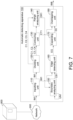
- FIG. 7 shows an automatic detecting apparatus 100 for detecting the etched via hole(s) VH1.
- the automatic detecting apparatus 100 helps the operators to automatically detect the residues RD1 in the etched via hole(s) VH1 without any human power.
- the automatic detecting apparatus 100 includes an inputting unit 110, a dividing unit 120, a contouring unit 130, a range analyzing unit 140, a boundary analyzing unit 150, an edge detecting unit 160, an expanding unit 170 and an overlapping unit 180.
- the inputting unit 110 is used to input data.
- the inputting unit 110 may be a wireless transmission module, a connecting line, or a card reader.
- the dividing unit 120, the contouring unit 130, the range analyzing unit 140, the boundary analyzing unit 150, the edge detecting unit 160, the expanding unit 170 and the overlapping unit 180 are used to perform several image processing steps.
- Each of the dividing unit 120, the contouring unit 130, the range analyzing unit 140, the boundary analyzing unit 150, the edge detecting unit 160, the expanding unit 170 and the overlapping unit 180 may be a circuit, a chip , a circuit board or a storage device storing a plurality of program codes. The operation of those elements is illustrated via a flowchart.
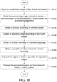
- FIG. 8 shows a flowchart of an automatic detecting method for detecting the etched via hole(s) VH1 according to one embodiment.
- FIG. 9 illustrates each of the steps in FIG. 8 .
- the inputting unit 110 inputs (or receives) the top-view image IM1 of the etched via hole(s) VH1.
- the top-view image IM1 is a monochrome grayscale image.
- the top-view image IM1 may be transmitted from a processing machine 800 through the network 900.
- step S120 the dividing unit 120 divides the top-view image IM1 into a first cluster C1, a second cluster C2, a third cluster C3 and a fourth cluster C4 in the top-view image IM1 via a clustering algorithm.
- the clustering algorithm is a K-means algorithm.
- the top-view image IM1 is divided according to a plurality of grayscale values.
- the first cluster C1 represents the top surface M1a of the metal line M1
- the second cluster C2 represents the residues RD1
- the third cluster C3 represents the top surface IL1a of the insulation layer IL1
- the fourth cluster C4 represents the sidewall VH1a of the etched via hole(s) VH1.
- the first cluster C1 is the darkest among the first cluster C1, the second cluster C2, the third cluster C3 and the fourth cluster C4.
- the fourth cluster C4 is the whitest among the first cluster C1, the second cluster C2, the third cluster C3 and the fourth cluster C4.
- the contouring unit 130 obtains a contour CT1 according to the first cluster C1.
- a first average pixel value of the first cluster C1 is larger than a second average pixel value of the second cluster C2, a third average pixel value of the third cluster C3 and a fourth average pixel value of the fourth cluster C4.
- the contouring unit 130 performs a binarization process based on the first cluster C1 to obtain the contour CT1.
- the pixel values of the pixels in the first cluster C1 are changed to be "1" and the pixel values of the pixels in the second cluster C2, the third cluster C3 and the fourth cluster C4 are changed to be "0.”
- the first cluster C1 represents the top surface M1a of the metal line M1, so the contour CT1 obtained according to the first cluster C1 is probably the contour of the residues RD1.
- step S140 the range analyzing unit 140 obtains a detecting range DR1 according to the fourth cluster C4.
- the fourth average pixel value of the fourth cluster C4 is less than the first average pixel value of the first cluster C1, the second average pixel value of the second cluster C2 and the third average pixel value of the third cluster C3.
- the range analyzing unit 140 performs a binarization process based on the fourth cluster C4 to obtain the detecting range DR1. For example, the internal in fourth cluster C4 is changed to be "1" and others are changed to be "0.”
- step S150 the boundary analyzing unit 150 obtains a circular boundary CB1 in the detecting range DR1.
- the boundary analyzing unit 150 overlaps the detecting range DR1 and the contour CT1 to obtain a union pattern UN1.
- the boundary analyzing unit 150 calculates an X coordinate and a radius of a center of the circular boundary CB1 according to the leftmost point and the rightmost point of the union pattern UN1.
- the boundary analyzing unit 150 calculates a Y coordinate of the center of the circular boundary CB1 according to the radius and the top point and the bottom point of the union pattern UN1.
- the circular boundary CB1 maybe an inscribed circle of the detecting range DR1.
- the circular boundary CB1 is used to define a limited area where the residues RD1 may be located.
- the detecting range DR1 represents the sidewall VH1a (shown in FIG. 5 ) of the etched via hole(s) VH1, so the circular boundary CB1 is limited within the sidewall VH1a of the etched via hole(s) VH1.
- step S160 the edge detecting unit 160 obtains a plurality of edges EG inside the circular boundary CB1. Those edges EG probably are formed by the rough surfaces of the residues RD1.
- step S170 the expanding unit 170 expands the edges EG to obtain a plurality of expanded edges EE.
- a n*n kernel matrix can be used to increase the width of n/2 pixels.
- a 15*15 kernel matrix can be used to increase the width of 7 pixels.
- the expanding unit 170 magnifies the edges EG by 2 to 4 times. Because the edges EG probably are formed by the rough surfaces of the residues RD1, the expanded edges EE are probably the residues RD1.
- step S180 the overlapping unit 180 overlaps the expanded edges EE and the contour CT1 to obtain a defect pattern IM8 containing the residues RD1. Because the expanded edges EE are probably the residues RD1, so the residues RD1 can be obtained by overlapping the expanded edges EE and the contour CT1.
- the automatic detecting method and the automatic detecting apparatus 100 help the operators to automatically detect the residues RD1 in the etched via hole(s) VH1 without any human power. Therefore, 100% inspection for a lot of etched via holes is possible.
Landscapes
- Engineering & Computer Science (AREA)
- Physics & Mathematics (AREA)
- Computer Vision & Pattern Recognition (AREA)
- General Physics & Mathematics (AREA)
- Theoretical Computer Science (AREA)
- Quality & Reliability (AREA)
- Geometry (AREA)
- Image Analysis (AREA)
Description
- The disclosure relates in general to a detecting method and a detecting apparatus using the same, and more particularly to an automatic detecting method and an automatic detecting apparatus using the same.
- Along with the development of semiconductor, several novel semiconductor devices are invented. In the semiconductor devices, metal lines located at different layer may be electrically connected through a via hole filled with a conductive material.
- The via hole may be formed by etching an insulation layer. However, if a residue is remained in an etched via hole, the conductivity may be greatly reduced. Therefore, the researchers try to develop an automatic detecting apparatus for detecting the etched via hole.
- From
US-A-2018/0088060 a method of inspecting patterns formed the manufacturing of semiconductor devices or the like is known which includes producing an image of the patterns, producing a boundary image including a plurality of boundary patterns corresponding to first and second boundary of each of the patterns, combing the pattern image and the boundary image to produce an overlapping image including overlapping patterns in which the patterns fill regions between the boundary patterns, and binarizing the overlapping image to produce a binary image including binary patterns corresponding to the overlapping patterns. - The disclosure is directed to an automatic detecting method as defined in claim 8 and an automatic detecting apparatus using the same as defined in claim 1. By performing several image processing steps, residues in an etched via hole can be automatically detected without any human power. Therefore, 100% inspection for a plurality of etched via holes is possible. Individual embodiments of the invention are the subject matter of the dependent claims.
- According to one embodiment, an automatic detecting apparatus for detecting an etched via hole is provided. The automatic detecting apparatus includes an inputting unit, a dividing unit, a contouring unit, a range analyzing unit, a boundary analyzing unit, an edge detecting unit, an expanding unit and an overlapping unit. The inputting unit is used for inputting a top-view image of the etched via hole. The dividing unit is used for dividing the top-view image into a first cluster, a second cluster, a third cluster and a fourth cluster via a clustering algorithm. The contouring unit is used for obtaining a contour according to the first cluster. A first average pixel value of the first cluster is larger than a second average pixel value of the second cluster, a third average pixel value of the third cluster and a fourth average pixel value of the fourth cluster. The range analyzing unit is used for obtaining a detecting range according to the fourth cluster. The fourth average pixel value of the fourth cluster is less than the first average pixel value of the first cluster, the second average pixel value of the second cluster and the third average pixel value of the third cluster. The boundary analyzing unit is used for obtaining a circular boundary in the detecting range. The edge detecting unit is used for obtaining a plurality of edges in the circular boundary. The expanding unit is used for expanding the edges to obtain a plurality of expanded edges. The overlapping unit is used for overlapping the expanded edges and the contour to obtain a defect pattern.
- According to another embodiment, an automatic detecting method for detecting an etched via hole is provided. A top-view image of the etched via hole is inputted. The top-view image is divided into a first cluster, a second cluster, a third cluster and a fourth cluster in the top-view image via a clustering algorithm. A contour is obtained according to the first cluster. A first average pixel value of the first cluster is larger than a second average pixel value of the second cluster, a third average pixel value of the third cluster and a fourth average pixel value of the fourth cluster. A detecting range is obtained according to the fourth cluster. The fourth average pixel value of the fourth cluster is less than the first average pixel value of the first cluster, the second average pixel value of the second cluster and the third average pixel value of the third cluster. At least one circular boundary is obtained in the detecting range. A plurality of edges inside the circular boundary are obtained. The edges are expanded to obtain a plurality of expanded edges. The expanded edges and the contour are overlapped to obtain a defect pattern.
-
-
FIG. 1 shows a top-view image of a plurality of etched via holes. -
FIG. 2 shows a cross-section view of the etched via holes along a section line A-A. -
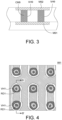
FIG. 3 shows another metal line. -
FIG. 4 shows a top-view image of a plurality of etched via holes. -
FIG. 5 shows a cross-section view of the etched via holes along a section line B-B'. -
FIG. 6 shows another metal line. -
FIG. 7 shows an automatic detecting apparatus for detecting the etched via hole(s). -
FIG. 8 shows a flowchart of an automatic detecting method for detecting the etched via hole(s) according to one embodiment. -
FIG. 9 illustrates each of the steps inFIG. 8 . - In the following detailed description, for purposes of explanation, numerous specific details are set forth in order to provide a thorough understanding of the disclosed embodiments. It will be apparent, however, that one or more embodiments may be practiced without these specific details. In other instances, well-known structures and devices are schematically shown in order to simplify the drawing.
- Please refer to
FIG. 1 , which shows a top-view image IM9 of a plurality of etched via holes VH9. In one embodiment, the top-view image IM9 is a Scanning Electron Microscope (SEM) image. InFIG. 1 , the etched via holes VH9 are well etched without any residue. Please refer toFIG. 2 , which shows a cross-section view of the etched via holes VH9 along a section line A-A'. An insulation layer IL9 is etched, by wet-etching or dry-etching, to form the etched via holes VH9. The etched via holes VH9 exposure a top surface M91a of a metal line M91. Please refer toFIG. 3 , which shows another metal line M92. The etched via holes VH9 are filled with a conductive material CM9 and the metal line M92 is formed on the conductive material CM9, such that the metal line M91 and the metal line M92 are electrically connected with each other through the conductive material CM9 filled in the etched via holes VH9. - Please refer to
FIG. 4 , which shows a top-view image IM1 of a plurality of etched via holes VH1. In one embodiment, the top-view image IM9 is a Scanning Electron Microscope (SEM) image. InFIG. 4 , the etched via holes VH1 are not well etched and some residues RD1 are remained. Please refer toFIG. 5 , which shows a cross-section view of the etched via holes VH1 along a section line B-B'. An insulation layer IL1 is etched, by wet-etching or dry-etching, to form the etched via holes VH1. The etched via holes VH1 exposure a top surface M1a of a metal line M1. Please refer toFIG. 6 , which shows another metal line M2. The etched via holes VH1 are filled with a conductive material CM1 and the metal line M2 is formed on the conductive material CM1, such that the metal line M1 and the metal line M2 are electrically connected with each other through the conductive material CM1 filled in the etched via holes VH1. As shown inFIG. 6 , the residues RD1 are remained on the top surface M1a, so the conductivity between the metal line M1 and the metal line M2 is reduced. - Please refer to
FIG. 7 , which shows an automatic detecting apparatus 100 for detecting the etched via hole(s) VH1. The automatic detecting apparatus 100 helps the operators to automatically detect the residues RD1 in the etched via hole(s) VH1 without any human power. - The automatic detecting apparatus 100 includes an
inputting unit 110, adividing unit 120, acontouring unit 130, arange analyzing unit 140, aboundary analyzing unit 150, anedge detecting unit 160, an expandingunit 170 and an overlappingunit 180. The inputtingunit 110 is used to input data. For example, the inputtingunit 110 may be a wireless transmission module, a connecting line, or a card reader. The dividingunit 120, thecontouring unit 130, therange analyzing unit 140, theboundary analyzing unit 150, theedge detecting unit 160, the expandingunit 170 and the overlappingunit 180 are used to perform several image processing steps. Each of thedividing unit 120, thecontouring unit 130, therange analyzing unit 140, theboundary analyzing unit 150, theedge detecting unit 160, the expandingunit 170 and the overlappingunit 180 may be a circuit, a chip , a circuit board or a storage device storing a plurality of program codes. The operation of those elements is illustrated via a flowchart. - Please refer to
FIGS. 7 to 9 .FIG. 8 shows a flowchart of an automatic detecting method for detecting the etched via hole(s) VH1 according to one embodiment.FIG. 9 illustrates each of the steps inFIG. 8 . In step S110, the inputtingunit 110 inputs (or receives) the top-view image IM1 of the etched via hole(s) VH1. In one embodiment, the top-view image IM1 is a monochrome grayscale image. The top-view image IM1 may be transmitted from aprocessing machine 800 through thenetwork 900. - Then, in step S120, the dividing
unit 120 divides the top-view image IM1 into a first cluster C1, a second cluster C2, a third cluster C3 and a fourth cluster C4 in the top-view image IM1 via a clustering algorithm. In one embodiment, the clustering algorithm is a K-means algorithm. The top-view image IM1 is divided according to a plurality of grayscale values. - Referring to both of
FIG. 5 andFIG. 9 , the first cluster C1 represents the top surface M1a of the metal line M1, the second cluster C2 represents the residues RD1, the third cluster C3 represents the top surface IL1a of the insulation layer IL1, and the fourth cluster C4 represents the sidewall VH1a of the etched via hole(s) VH1. As shown inFIG. 9 , the first cluster C1 is the darkest among the first cluster C1, the second cluster C2, the third cluster C3 and the fourth cluster C4. The fourth cluster C4 is the whitest among the first cluster C1, the second cluster C2, the third cluster C3 and the fourth cluster C4. - Afterwards, in step S130, the
contouring unit 130 obtains a contour CT1 according to the first cluster C1. A first average pixel value of the first cluster C1 is larger than a second average pixel value of the second cluster C2, a third average pixel value of the third cluster C3 and a fourth average pixel value of the fourth cluster C4. In one embodiment, thecontouring unit 130 performs a binarization process based on the first cluster C1 to obtain the contour CT1. For example, the pixel values of the pixels in the first cluster C1 are changed to be "1" and the pixel values of the pixels in the second cluster C2, the third cluster C3 and the fourth cluster C4 are changed to be "0." The first cluster C1 represents the top surface M1a of the metal line M1, so the contour CT1 obtained according to the first cluster C1 is probably the contour of the residues RD1. - Next, in step S140, the
range analyzing unit 140 obtains a detecting range DR1 according to the fourth cluster C4. The fourth average pixel value of the fourth cluster C4 is less than the first average pixel value of the first cluster C1, the second average pixel value of the second cluster C2 and the third average pixel value of the third cluster C3. In one embodiment, therange analyzing unit 140 performs a binarization process based on the fourth cluster C4 to obtain the detecting range DR1. For example, the internal in fourth cluster C4 is changed to be "1" and others are changed to be "0." - Further, as shown in
FIG. 9 , in case of that one fourth cluster C4 corresponds two contours CT1, two detecting ranges DR1 will be obtained in this fourth cluster C4. - Then, in step S150, the
boundary analyzing unit 150 obtains a circular boundary CB1 in the detecting range DR1. In one embodiment, theboundary analyzing unit 150 overlaps the detecting range DR1 and the contour CT1 to obtain a union pattern UN1. Then, theboundary analyzing unit 150 calculates an X coordinate and a radius of a center of the circular boundary CB1 according to the leftmost point and the rightmost point of the union pattern UN1. Afterwards, theboundary analyzing unit 150 calculates a Y coordinate of the center of the circular boundary CB1 according to the radius and the top point and the bottom point of the union pattern UN1. In another embodiment, the circular boundary CB1 maybe an inscribed circle of the detecting range DR1. - The circular boundary CB1 is used to define a limited area where the residues RD1 may be located. For example, the detecting range DR1 represents the sidewall VH1a (shown in
FIG. 5 ) of the etched via hole(s) VH1, so the circular boundary CB1 is limited within the sidewall VH1a of the etched via hole(s) VH1. - Afterwards, in step S160, the
edge detecting unit 160 obtains a plurality of edges EG inside the circular boundary CB1. Those edges EG probably are formed by the rough surfaces of the residues RD1. - Next, in step S170, the expanding
unit 170 expands the edges EG to obtain a plurality of expanded edges EE. In the image processing process, a n*n kernel matrix can be used to increase the width of n/2 pixels. For example, a 15*15 kernel matrix can be used to increase the width of 7 pixels. In another embodiment, the expandingunit 170 magnifies the edges EG by 2 to 4 times. Because the edges EG probably are formed by the rough surfaces of the residues RD1, the expanded edges EE are probably the residues RD1. - Then, in step S180, the overlapping
unit 180 overlaps the expanded edges EE and the contour CT1 to obtain a defect pattern IM8 containing the residues RD1. Because the expanded edges EE are probably the residues RD1, so the residues RD1 can be obtained by overlapping the expanded edges EE and the contour CT1. - According to the embodiments described above, by performing several image processing steps, the automatic detecting method and the automatic detecting apparatus 100 help the operators to automatically detect the residues RD1 in the etched via hole(s) VH1 without any human power. Therefore, 100% inspection for a lot of etched via holes is possible.
- It will be apparent to those skilled in the art that various modifications and variations can be made to the disclosed embodiments. It is intended that the specification and examples be considered as exemplary only, with a true scope of the disclosure being indicated by the following claims and their equivalents.
Claims (15)
- An automatic detecting apparatus (100) for detecting an etched via hole (VH1), the automatic detecting apparatus (100) comprising:an inputting unit (110) for inputting a top-view image (IM1) of the etched via hole (VH1);a dividing unit (120) for dividing the top-view image (IM1) into a first cluster (C1), a second cluster (C2), a third cluster (C3) and a fourth cluster (C4) via a clustering algorithm according to a plurality of grayscale values of the top-view image (IM1);a contouring unit (130) for obtaining a contour (CT1) in the top-view image (IM1) according to the first cluster (C1), wherein a first average pixel value of the first cluster (C1) is larger than a second average pixel value of the second cluster (C2), a third average pixel value of the third cluster (C3) and a fourth average pixel value of the fourth cluster (C4);a range analyzing unit (140) for obtaining a detecting range (DR1) in the top-view image (IM1) according to the fourth cluster (C4), wherein the fourth average pixel value of the fourth cluster (C4) is less than the first average pixel value of the first cluster (C1), the second average pixel value of the second cluster (C2) and the third average pixel value of the third cluster (C3);a boundary analyzing unit (150) for obtaining a circular boundary (CB1) in the detecting range (DR1);an edge detecting unit (160) for obtaining a plurality of edges (EG) in the circular boundary (CB1);an expanding unit (170) for expanding the edges (EG) to obtain a plurality of expanded edges (EE); andan overlapping unit (180) for overlapping the expanded edges (EE) and the contour (CT1) to obtain a defect pattern (IM8).
- The automatic detecting apparatus according to claim 1, wherein the top-view image is a monochrome grayscale image.
- The automatic detecting apparatus according to claim 1 or 2, wherein the dividing unit divides the top-view image according to a plurality of grayscale values.
- The automatic detecting apparatus according to any of claims 1 to 3, wherein the countering unit performs a binarization process based on the first cluster to obtain the counter.
- The automatic detecting apparatus according to any of claims 1 to 4, wherein the range analyzing unit performs a binarization process based on the fourth cluster to obtain the detecting range.
- The automatic detecting apparatus according to any of claims 1 to 5, wherein the boundary analyzing unit overlaps the detecting range and the contour to obtain an union pattern, and the boundary analyzing unit obtain the circular boundary according to a leftmost point, a rightmost point, a top point and a bottom point of the union pattern.
- The automatic detecting apparatus according to claim 6, wherein the boundary analyzing unit calculates an X coordinate and a radius of a center of the circular boundary according to the leftmost point and the rightmost point of the union pattern, then the boundary analyzing unit calculates a Y coordinate of the center of the circular boundary according to the radius and the top point and the bottom point of the union pattern.
- An automatic detecting method for detecting an etched via hole (VH1), the automatic detecting method comprising:inputting a top-view image (IM1) of the etched via hole (VH1);dividing the top-view image (IM1) into a first cluster (C1), a second cluster (C2), a third cluster (C3) and a fourth cluster (C4) in the overlooking image (IM1) via a clustering algorithm;obtaining a contour (CT1) in the top-view image (IM1) according to the first cluster (C1), wherein a first average pixel value of the first cluster (C1) is larger than a second average pixel value of the second cluster (C2), a third average pixel value of the third cluster (C3) and a fourth average pixel value of the fourth cluster (C4);obtaining a detecting range (DR1) in the top-view image (IM1) according to the fourth cluster (C4), wherein the fourth average pixel value of the fourth cluster (C4) is less than the first average pixel value of the first cluster (C1), the second average pixel value of the second cluster (C2) and the third average pixel value of the third cluster (C3);obtaining a circular boundary (CB1) in the detecting range (DR1);obtaining a plurality of edges (EG) inside the circular boundary (CB1);expanding the edges (EG) to obtain a plurality of expanded edges (EE); andoverlapping the expanded edges (EE) and the contour (CT1) to obtain a defect pattern (IM8).
- The automatic detecting method according to claim 8, wherein in the step of inputting the top-view image, the top-view image is a monochrome grayscale image.
- The automatic detecting method according to claim 8 or 9, wherein in the step of dividing the top-view image, the top-view image is divided according to a plurality of grayscale values.
- The automatic detecting method according to any of claims 8 to 10, wherein in the step of obtaining the contour, a binarization process is performed based on the first cluster.
- The automatic detecting method according to any of claims 8 to 11, wherein in the step of obtaining the detecting range, a binarization process is performed based on the fourth cluster.
- The automatic detecting method according to any of claims 8 to 12, wherein in the step of obtaining the circular boundary, the detecting range and the contour are overlapped to obtain an union pattern, and the circular boundary is obtained according to a leftmost point, a rightmost point, a top point and a bottom point of the union pattern.
- The automatic detecting method according to claim 13, wherein an X coordinate and a radius of a center of the circular boundary are calculated according to the leftmost point and the rightmost point of the union pattern, a Y coordinate of the center of the circular boundary is calculated according to the radius and the top point and the bottom point of the union pattern.
- The automatic detecting method according to any of claims 8 to 14, wherein in the step of obtaining the circular boundary, the circular boundary is an inscribed circle of the detecting range.
Applications Claiming Priority (1)
| Application Number | Priority Date | Filing Date | Title |
|---|---|---|---|
| US16/429,772 US11151724B2 (en) | 2019-06-03 | 2019-06-03 | Automatic detecting method and automatic detecting apparatus using the same |
Publications (2)
| Publication Number | Publication Date |
|---|---|
| EP3748578A1 EP3748578A1 (en) | 2020-12-09 |
| EP3748578B1 true EP3748578B1 (en) | 2023-07-05 |
Family
ID=70475994
Family Applications (1)
| Application Number | Title | Priority Date | Filing Date |
|---|---|---|---|
| EP20171769.1A Active EP3748578B1 (en) | 2019-06-03 | 2020-04-28 | Automatic visual detection of defects in images of via holes |
Country Status (2)
| Country | Link |
|---|---|
| US (1) | US11151724B2 (en) |
| EP (1) | EP3748578B1 (en) |
Families Citing this family (4)
| Publication number | Priority date | Publication date | Assignee | Title |
|---|---|---|---|---|
| US10522322B2 (en) | 2017-04-13 | 2019-12-31 | Fractilia, Llc | System and method for generating and analyzing roughness measurements |
| US10176966B1 (en) | 2017-04-13 | 2019-01-08 | Fractilia, Llc | Edge detection system |
| US11380516B2 (en) | 2017-04-13 | 2022-07-05 | Fractilia, Llc | System and method for generating and analyzing roughness measurements and their use for process monitoring and control |
| US12142454B2 (en) | 2017-04-13 | 2024-11-12 | Fractilla, LLC | Detection of probabilistic process windows |
Family Cites Families (10)
| Publication number | Priority date | Publication date | Assignee | Title |
|---|---|---|---|---|
| US5150422A (en) * | 1989-03-31 | 1992-09-22 | Dainippon Screen Mfg. Co., Ltd. | Method of and apparatus for inspecting conductive pattern on printed board |
| US5214712A (en) * | 1990-09-11 | 1993-05-25 | Matsushita Electric Industrial Co., Ltd. | Pattern inspection system for inspecting defect of land pattern for through-hole on printed board |
| US5923430A (en) * | 1993-06-17 | 1999-07-13 | Ultrapointe Corporation | Method for characterizing defects on semiconductor wafers |
| US7149340B2 (en) | 2002-09-20 | 2006-12-12 | Lsi Logic Corporation | Mask defect analysis for both horizontal and vertical processing effects |
| US7171047B2 (en) | 2002-12-20 | 2007-01-30 | Lsi Logic Corporation | Adaptive Sem edge recognition algorithm |
| US9052294B2 (en) * | 2006-05-31 | 2015-06-09 | The Boeing Company | Method and system for two-dimensional and three-dimensional inspection of a workpiece |
| US8401273B2 (en) | 2010-01-21 | 2013-03-19 | Hitachi, Ltd. | Apparatus for evaluating degradation of pattern features |
| US20160292845A1 (en) | 2015-03-31 | 2016-10-06 | Macronix International Co., Ltd. | Determining contact edge roughness of a contact hole etched in a wafer |
| KR102773390B1 (en) * | 2016-09-23 | 2025-02-28 | 삼성전자주식회사 | Method for measuring pattern and method for manufacturing semiconductor device including the same |
| US10839507B2 (en) * | 2017-11-30 | 2020-11-17 | Taiwan Semiconductor Manufacturing Co., Ltd. | Defect offset correction |
-
2019
- 2019-06-03 US US16/429,772 patent/US11151724B2/en active Active
-
2020
- 2020-04-28 EP EP20171769.1A patent/EP3748578B1/en active Active
Also Published As
| Publication number | Publication date |
|---|---|
| US20200380693A1 (en) | 2020-12-03 |
| EP3748578A1 (en) | 2020-12-09 |
| US11151724B2 (en) | 2021-10-19 |
Similar Documents
| Publication | Publication Date | Title |
|---|---|---|
| EP3748578A1 (en) | Automatic visual detection of defects in images of via holes | |
| JP3435684B2 (en) | Image information processing device | |
| TWI539150B (en) | System, method and computer program product for detection of defects within inspection images | |
| CN113096119A (en) | Method and device for classifying wafer defects, electronic equipment and storage medium | |
| US10043090B2 (en) | Information processing device, information processing method, computer-readable recording medium, and inspection system | |
| KR101565748B1 (en) | A method and apparatus for detecting a repetitive pattern in image | |
| JP7427744B2 (en) | Image processing program, image processing device, image processing method, and defect detection system | |
| US20060238755A1 (en) | Method for analyzing defect data and inspection apparatus and review system | |
| US20030017664A1 (en) | Kill index analysis for automatic defect classification in semiconductor wafers | |
| CN113487569B (en) | Complex background image defect detection method and system based on combination of frequency domain and space domain | |
| CN113506243A (en) | PCB welding defect detection method and device and storage medium | |
| CN116994976A (en) | Method, device, medium and wafer processing method for identifying wafer edge defect types | |
| CN114509446B (en) | Wafer unfilled corner automatic detection method and wafer unfilled corner automatic detection system | |
| KR101521620B1 (en) | method of segmentation of die image for semiconductor device examination | |
| WO2023166748A1 (en) | Profile detection method and profile detection device | |
| KR19990049102A (en) | Wafer defect classification method | |
| US6005966A (en) | Method and apparatus for multi-stream detection of high density metalization layers of multilayer structures having low contrast | |
| KR102879958B1 (en) | Apparatus and method for finding optimal width for inspection of 3d film images | |
| CN113554585B (en) | Image analysis system and image analysis method | |
| JPH064674A (en) | Method and apparatus for removing unnecessary boundary pixels in area division | |
| JP2008508622A (en) | Surface inspection method | |
| CN116358411B (en) | Contact positioning method, contact positioning device, probe station and storage medium | |
| CN120782739A (en) | Pretreatment method for wafer defect detection and computer program product | |
| CN119580021A (en) | A wafer defect classification method and device based on wafer image | |
| CN120707493A (en) | Linear roughness measurement method based on scanning electron microscope images |
Legal Events
| Date | Code | Title | Description |
|---|---|---|---|
| PUAI | Public reference made under article 153(3) epc to a published international application that has entered the european phase |
Free format text: ORIGINAL CODE: 0009012 |
|
| STAA | Information on the status of an ep patent application or granted ep patent |
Free format text: STATUS: REQUEST FOR EXAMINATION WAS MADE |
|
| 17P | Request for examination filed |
Effective date: 20200428 |
|
| AK | Designated contracting states |
Kind code of ref document: A1 Designated state(s): AL AT BE BG CH CY CZ DE DK EE ES FI FR GB GR HR HU IE IS IT LI LT LU LV MC MK MT NL NO PL PT RO RS SE SI SK SM TR |
|
| AX | Request for extension of the european patent |
Extension state: BA ME |
|
| RBV | Designated contracting states (corrected) |
Designated state(s): AL AT BE BG CH CY CZ DE DK EE ES FI FR GB GR HR HU IE IS IT LI LT LU LV MC MK MT NL NO PL PT RO RS SE SI SK SM TR |
|
| GRAP | Despatch of communication of intention to grant a patent |
Free format text: ORIGINAL CODE: EPIDOSNIGR1 |
|
| STAA | Information on the status of an ep patent application or granted ep patent |
Free format text: STATUS: GRANT OF PATENT IS INTENDED |
|
| RIC1 | Information provided on ipc code assigned before grant |
Ipc: G01N 23/2251 20180101ALN20230201BHEP Ipc: H01L 21/66 20060101ALI20230201BHEP Ipc: G06T 7/136 20170101ALI20230201BHEP Ipc: G06T 7/13 20170101ALI20230201BHEP Ipc: G06T 7/00 20060101AFI20230201BHEP |
|
| INTG | Intention to grant announced |
Effective date: 20230220 |
|
| GRAS | Grant fee paid |
Free format text: ORIGINAL CODE: EPIDOSNIGR3 |
|
| GRAA | (expected) grant |
Free format text: ORIGINAL CODE: 0009210 |
|
| STAA | Information on the status of an ep patent application or granted ep patent |
Free format text: STATUS: THE PATENT HAS BEEN GRANTED |
|
| AK | Designated contracting states |
Kind code of ref document: B1 Designated state(s): AL AT BE BG CH CY CZ DE DK EE ES FI FR GB GR HR HU IE IS IT LI LT LU LV MC MK MT NL NO PL PT RO RS SE SI SK SM TR |
|
| REG | Reference to a national code |
Ref country code: CH Ref legal event code: EP |
|
| REG | Reference to a national code |
Ref country code: AT Ref legal event code: REF Ref document number: 1585537 Country of ref document: AT Kind code of ref document: T Effective date: 20230715 |
|
| REG | Reference to a national code |
Ref country code: DE Ref legal event code: R096 Ref document number: 602020013179 Country of ref document: DE |
|
| REG | Reference to a national code |
Ref country code: IE Ref legal event code: FG4D |
|
| REG | Reference to a national code |
Ref country code: LT Ref legal event code: MG9D |
|
| REG | Reference to a national code |
Ref country code: NL Ref legal event code: MP Effective date: 20230705 |
|
| REG | Reference to a national code |
Ref country code: AT Ref legal event code: MK05 Ref document number: 1585537 Country of ref document: AT Kind code of ref document: T Effective date: 20230705 |
|
| PG25 | Lapsed in a contracting state [announced via postgrant information from national office to epo] |
Ref country code: NL Free format text: LAPSE BECAUSE OF FAILURE TO SUBMIT A TRANSLATION OF THE DESCRIPTION OR TO PAY THE FEE WITHIN THE PRESCRIBED TIME-LIMIT Effective date: 20230705 |
|
| PG25 | Lapsed in a contracting state [announced via postgrant information from national office to epo] |
Ref country code: GR Free format text: LAPSE BECAUSE OF FAILURE TO SUBMIT A TRANSLATION OF THE DESCRIPTION OR TO PAY THE FEE WITHIN THE PRESCRIBED TIME-LIMIT Effective date: 20231006 |
|
| PG25 | Lapsed in a contracting state [announced via postgrant information from national office to epo] |
Ref country code: ES Free format text: LAPSE BECAUSE OF FAILURE TO SUBMIT A TRANSLATION OF THE DESCRIPTION OR TO PAY THE FEE WITHIN THE PRESCRIBED TIME-LIMIT Effective date: 20230705 |
|
| PG25 | Lapsed in a contracting state [announced via postgrant information from national office to epo] |
Ref country code: IS Free format text: LAPSE BECAUSE OF FAILURE TO SUBMIT A TRANSLATION OF THE DESCRIPTION OR TO PAY THE FEE WITHIN THE PRESCRIBED TIME-LIMIT Effective date: 20231105 |
|
| PG25 | Lapsed in a contracting state [announced via postgrant information from national office to epo] |
Ref country code: SE Free format text: LAPSE BECAUSE OF FAILURE TO SUBMIT A TRANSLATION OF THE DESCRIPTION OR TO PAY THE FEE WITHIN THE PRESCRIBED TIME-LIMIT Effective date: 20230705 Ref country code: RS Free format text: LAPSE BECAUSE OF FAILURE TO SUBMIT A TRANSLATION OF THE DESCRIPTION OR TO PAY THE FEE WITHIN THE PRESCRIBED TIME-LIMIT Effective date: 20230705 Ref country code: PT Free format text: LAPSE BECAUSE OF FAILURE TO SUBMIT A TRANSLATION OF THE DESCRIPTION OR TO PAY THE FEE WITHIN THE PRESCRIBED TIME-LIMIT Effective date: 20231106 Ref country code: NO Free format text: LAPSE BECAUSE OF FAILURE TO SUBMIT A TRANSLATION OF THE DESCRIPTION OR TO PAY THE FEE WITHIN THE PRESCRIBED TIME-LIMIT Effective date: 20231005 Ref country code: LV Free format text: LAPSE BECAUSE OF FAILURE TO SUBMIT A TRANSLATION OF THE DESCRIPTION OR TO PAY THE FEE WITHIN THE PRESCRIBED TIME-LIMIT Effective date: 20230705 Ref country code: LT Free format text: LAPSE BECAUSE OF FAILURE TO SUBMIT A TRANSLATION OF THE DESCRIPTION OR TO PAY THE FEE WITHIN THE PRESCRIBED TIME-LIMIT Effective date: 20230705 Ref country code: IS Free format text: LAPSE BECAUSE OF FAILURE TO SUBMIT A TRANSLATION OF THE DESCRIPTION OR TO PAY THE FEE WITHIN THE PRESCRIBED TIME-LIMIT Effective date: 20231105 Ref country code: HR Free format text: LAPSE BECAUSE OF FAILURE TO SUBMIT A TRANSLATION OF THE DESCRIPTION OR TO PAY THE FEE WITHIN THE PRESCRIBED TIME-LIMIT Effective date: 20230705 Ref country code: GR Free format text: LAPSE BECAUSE OF FAILURE TO SUBMIT A TRANSLATION OF THE DESCRIPTION OR TO PAY THE FEE WITHIN THE PRESCRIBED TIME-LIMIT Effective date: 20231006 Ref country code: FI Free format text: LAPSE BECAUSE OF FAILURE TO SUBMIT A TRANSLATION OF THE DESCRIPTION OR TO PAY THE FEE WITHIN THE PRESCRIBED TIME-LIMIT Effective date: 20230705 Ref country code: ES Free format text: LAPSE BECAUSE OF FAILURE TO SUBMIT A TRANSLATION OF THE DESCRIPTION OR TO PAY THE FEE WITHIN THE PRESCRIBED TIME-LIMIT Effective date: 20230705 Ref country code: AT Free format text: LAPSE BECAUSE OF FAILURE TO SUBMIT A TRANSLATION OF THE DESCRIPTION OR TO PAY THE FEE WITHIN THE PRESCRIBED TIME-LIMIT Effective date: 20230705 |
|
| PG25 | Lapsed in a contracting state [announced via postgrant information from national office to epo] |
Ref country code: PL Free format text: LAPSE BECAUSE OF FAILURE TO SUBMIT A TRANSLATION OF THE DESCRIPTION OR TO PAY THE FEE WITHIN THE PRESCRIBED TIME-LIMIT Effective date: 20230705 |
|
| REG | Reference to a national code |
Ref country code: DE Ref legal event code: R097 Ref document number: 602020013179 Country of ref document: DE |
|
| PG25 | Lapsed in a contracting state [announced via postgrant information from national office to epo] |
Ref country code: SM Free format text: LAPSE BECAUSE OF FAILURE TO SUBMIT A TRANSLATION OF THE DESCRIPTION OR TO PAY THE FEE WITHIN THE PRESCRIBED TIME-LIMIT Effective date: 20230705 Ref country code: RO Free format text: LAPSE BECAUSE OF FAILURE TO SUBMIT A TRANSLATION OF THE DESCRIPTION OR TO PAY THE FEE WITHIN THE PRESCRIBED TIME-LIMIT Effective date: 20230705 Ref country code: EE Free format text: LAPSE BECAUSE OF FAILURE TO SUBMIT A TRANSLATION OF THE DESCRIPTION OR TO PAY THE FEE WITHIN THE PRESCRIBED TIME-LIMIT Effective date: 20230705 Ref country code: DK Free format text: LAPSE BECAUSE OF FAILURE TO SUBMIT A TRANSLATION OF THE DESCRIPTION OR TO PAY THE FEE WITHIN THE PRESCRIBED TIME-LIMIT Effective date: 20230705 Ref country code: CZ Free format text: LAPSE BECAUSE OF FAILURE TO SUBMIT A TRANSLATION OF THE DESCRIPTION OR TO PAY THE FEE WITHIN THE PRESCRIBED TIME-LIMIT Effective date: 20230705 Ref country code: SK Free format text: LAPSE BECAUSE OF FAILURE TO SUBMIT A TRANSLATION OF THE DESCRIPTION OR TO PAY THE FEE WITHIN THE PRESCRIBED TIME-LIMIT Effective date: 20230705 |
|
| PLBE | No opposition filed within time limit |
Free format text: ORIGINAL CODE: 0009261 |
|
| STAA | Information on the status of an ep patent application or granted ep patent |
Free format text: STATUS: NO OPPOSITION FILED WITHIN TIME LIMIT |
|
| PG25 | Lapsed in a contracting state [announced via postgrant information from national office to epo] |
Ref country code: IT Free format text: LAPSE BECAUSE OF FAILURE TO SUBMIT A TRANSLATION OF THE DESCRIPTION OR TO PAY THE FEE WITHIN THE PRESCRIBED TIME-LIMIT Effective date: 20230705 |
|
| 26N | No opposition filed |
Effective date: 20240408 |
|
| PG25 | Lapsed in a contracting state [announced via postgrant information from national office to epo] |
Ref country code: SI Free format text: LAPSE BECAUSE OF FAILURE TO SUBMIT A TRANSLATION OF THE DESCRIPTION OR TO PAY THE FEE WITHIN THE PRESCRIBED TIME-LIMIT Effective date: 20230705 |
|
| PG25 | Lapsed in a contracting state [announced via postgrant information from national office to epo] |
Ref country code: BG Free format text: LAPSE BECAUSE OF FAILURE TO SUBMIT A TRANSLATION OF THE DESCRIPTION OR TO PAY THE FEE WITHIN THE PRESCRIBED TIME-LIMIT Effective date: 20230705 |
|
| PG25 | Lapsed in a contracting state [announced via postgrant information from national office to epo] |
Ref country code: MC Free format text: LAPSE BECAUSE OF FAILURE TO SUBMIT A TRANSLATION OF THE DESCRIPTION OR TO PAY THE FEE WITHIN THE PRESCRIBED TIME-LIMIT Effective date: 20230705 |
|
| PG25 | Lapsed in a contracting state [announced via postgrant information from national office to epo] |
Ref country code: MC Free format text: LAPSE BECAUSE OF FAILURE TO SUBMIT A TRANSLATION OF THE DESCRIPTION OR TO PAY THE FEE WITHIN THE PRESCRIBED TIME-LIMIT Effective date: 20230705 Ref country code: BG Free format text: LAPSE BECAUSE OF FAILURE TO SUBMIT A TRANSLATION OF THE DESCRIPTION OR TO PAY THE FEE WITHIN THE PRESCRIBED TIME-LIMIT Effective date: 20230705 |
|
| REG | Reference to a national code |
Ref country code: CH Ref legal event code: PL |
|
| PG25 | Lapsed in a contracting state [announced via postgrant information from national office to epo] |
Ref country code: LU Free format text: LAPSE BECAUSE OF NON-PAYMENT OF DUE FEES Effective date: 20240428 |
|
| GBPC | Gb: european patent ceased through non-payment of renewal fee |
Effective date: 20240428 |
|
| REG | Reference to a national code |
Ref country code: BE Ref legal event code: MM Effective date: 20240430 |
|
| PG25 | Lapsed in a contracting state [announced via postgrant information from national office to epo] |
Ref country code: LU Free format text: LAPSE BECAUSE OF NON-PAYMENT OF DUE FEES Effective date: 20240428 |
|
| PG25 | Lapsed in a contracting state [announced via postgrant information from national office to epo] |
Ref country code: BE Free format text: LAPSE BECAUSE OF NON-PAYMENT OF DUE FEES Effective date: 20240430 |
|
| PG25 | Lapsed in a contracting state [announced via postgrant information from national office to epo] |
Ref country code: GB Free format text: LAPSE BECAUSE OF NON-PAYMENT OF DUE FEES Effective date: 20240428 |
|
| PG25 | Lapsed in a contracting state [announced via postgrant information from national office to epo] |
Ref country code: FR Free format text: LAPSE BECAUSE OF NON-PAYMENT OF DUE FEES Effective date: 20240430 |
|
| PG25 | Lapsed in a contracting state [announced via postgrant information from national office to epo] |
Ref country code: GB Free format text: LAPSE BECAUSE OF NON-PAYMENT OF DUE FEES Effective date: 20240428 Ref country code: FR Free format text: LAPSE BECAUSE OF NON-PAYMENT OF DUE FEES Effective date: 20240430 Ref country code: BE Free format text: LAPSE BECAUSE OF NON-PAYMENT OF DUE FEES Effective date: 20240430 Ref country code: CH Free format text: LAPSE BECAUSE OF NON-PAYMENT OF DUE FEES Effective date: 20240430 |
|
| PG25 | Lapsed in a contracting state [announced via postgrant information from national office to epo] |
Ref country code: IE Free format text: LAPSE BECAUSE OF NON-PAYMENT OF DUE FEES Effective date: 20240428 |
|
| PGFP | Annual fee paid to national office [announced via postgrant information from national office to epo] |
Ref country code: DE Payment date: 20250428 Year of fee payment: 6 |
|
| PG25 | Lapsed in a contracting state [announced via postgrant information from national office to epo] |
Ref country code: CY Free format text: LAPSE BECAUSE OF FAILURE TO SUBMIT A TRANSLATION OF THE DESCRIPTION OR TO PAY THE FEE WITHIN THE PRESCRIBED TIME-LIMIT; INVALID AB INITIO Effective date: 20200428 |
|
| PG25 | Lapsed in a contracting state [announced via postgrant information from national office to epo] |
Ref country code: HU Free format text: LAPSE BECAUSE OF FAILURE TO SUBMIT A TRANSLATION OF THE DESCRIPTION OR TO PAY THE FEE WITHIN THE PRESCRIBED TIME-LIMIT; INVALID AB INITIO Effective date: 20200428 |