EP3742612A1 - Cryogenic radio-frequency resonator for surface ion traps - Google Patents
Cryogenic radio-frequency resonator for surface ion traps Download PDFInfo
- Publication number
- EP3742612A1 EP3742612A1 EP20174220.2A EP20174220A EP3742612A1 EP 3742612 A1 EP3742612 A1 EP 3742612A1 EP 20174220 A EP20174220 A EP 20174220A EP 3742612 A1 EP3742612 A1 EP 3742612A1
- Authority
- EP
- European Patent Office
- Prior art keywords
- cryogenic
- impedance
- thermally conductive
- signal
- matched
- Prior art date
- Legal status (The legal status is an assumption and is not a legal conclusion. Google has not performed a legal analysis and makes no representation as to the accuracy of the status listed.)
- Granted
Links
Images


Classifications
-
- H—ELECTRICITY
- H03—ELECTRONIC CIRCUITRY
- H03H—IMPEDANCE NETWORKS, e.g. RESONANT CIRCUITS; RESONATORS
- H03H9/00—Networks comprising electromechanical or electro-acoustic elements; Electromechanical resonators
- H03H9/24—Constructional features of resonators of material which is not piezoelectric, electrostrictive, or magnetostrictive
- H03H9/2405—Constructional features of resonators of material which is not piezoelectric, electrostrictive, or magnetostrictive of microelectro-mechanical resonators
-
- H—ELECTRICITY
- H03—ELECTRONIC CIRCUITRY
- H03H—IMPEDANCE NETWORKS, e.g. RESONANT CIRCUITS; RESONATORS
- H03H7/00—Multiple-port networks comprising only passive electrical elements as network components
- H03H7/01—Frequency selective two-port networks
- H03H7/17—Structural details of sub-circuits of frequency selective networks
-
- G—PHYSICS
- G04—HOROLOGY
- G04F—TIME-INTERVAL MEASURING
- G04F5/00—Apparatus for producing preselected time intervals for use as timing standards
- G04F5/14—Apparatus for producing preselected time intervals for use as timing standards using atomic clocks
-
- H—ELECTRICITY
- H03—ELECTRONIC CIRCUITRY
- H03H—IMPEDANCE NETWORKS, e.g. RESONANT CIRCUITS; RESONATORS
- H03H5/00—One-port networks comprising only passive electrical elements as network components
- H03H5/02—One-port networks comprising only passive electrical elements as network components without voltage- or current-dependent elements
- H03H5/10—One-port networks comprising only passive electrical elements as network components without voltage- or current-dependent elements comprising at least one element with prescribed temperature coefficient
-
- H—ELECTRICITY
- H03—ELECTRONIC CIRCUITRY
- H03H—IMPEDANCE NETWORKS, e.g. RESONANT CIRCUITS; RESONATORS
- H03H7/00—Multiple-port networks comprising only passive electrical elements as network components
- H03H7/01—Frequency selective two-port networks
- H03H7/0115—Frequency selective two-port networks comprising only inductors and capacitors
-
- H—ELECTRICITY
- H03—ELECTRONIC CIRCUITRY
- H03H—IMPEDANCE NETWORKS, e.g. RESONANT CIRCUITS; RESONATORS
- H03H7/00—Multiple-port networks comprising only passive electrical elements as network components
- H03H7/38—Impedance-matching networks
-
- H—ELECTRICITY
- H03—ELECTRONIC CIRCUITRY
- H03H—IMPEDANCE NETWORKS, e.g. RESONANT CIRCUITS; RESONATORS
- H03H9/00—Networks comprising electromechanical or electro-acoustic elements; Electromechanical resonators
- H03H9/02—Details
- H03H9/02244—Details of microelectro-mechanical resonators
-
- H—ELECTRICITY
- H03—ELECTRONIC CIRCUITRY
- H03H—IMPEDANCE NETWORKS, e.g. RESONANT CIRCUITS; RESONATORS
- H03H9/00—Networks comprising electromechanical or electro-acoustic elements; Electromechanical resonators
- H03H9/02—Details
- H03H9/02244—Details of microelectro-mechanical resonators
- H03H9/02433—Means for compensation or elimination of undesired effects
- H03H9/02448—Means for compensation or elimination of undesired effects of temperature influence
-
- H—ELECTRICITY
- H03—ELECTRONIC CIRCUITRY
- H03H—IMPEDANCE NETWORKS, e.g. RESONANT CIRCUITS; RESONATORS
- H03H9/00—Networks comprising electromechanical or electro-acoustic elements; Electromechanical resonators
- H03H9/02—Details
- H03H9/125—Driving means, e.g. electrodes, coils
-
- H—ELECTRICITY
- H01—ELECTRIC ELEMENTS
- H01F—MAGNETS; INDUCTANCES; TRANSFORMERS; SELECTION OF MATERIALS FOR THEIR MAGNETIC PROPERTIES
- H01F27/00—Details of transformers or inductances, in general
- H01F27/08—Cooling; Ventilating
- H01F27/22—Cooling by heat conduction through solid or powdered fillings
-
- H—ELECTRICITY
- H01—ELECTRIC ELEMENTS
- H01J—ELECTRIC DISCHARGE TUBES OR DISCHARGE LAMPS
- H01J49/00—Particle spectrometers or separator tubes
- H01J49/02—Details
- H01J49/022—Circuit arrangements, e.g. for generating deviation currents or voltages ; Components associated with high voltage supply
-
- H—ELECTRICITY
- H03—ELECTRONIC CIRCUITRY
- H03H—IMPEDANCE NETWORKS, e.g. RESONANT CIRCUITS; RESONATORS
- H03H1/00—Constructional details of impedance networks whose electrical mode of operation is not specified or applicable to more than one type of network
- H03H2001/0021—Constructional details
- H03H2001/005—Wound, ring or feed-through type inductor
-
- H—ELECTRICITY
- H03—ELECTRONIC CIRCUITRY
- H03H—IMPEDANCE NETWORKS, e.g. RESONANT CIRCUITS; RESONATORS
- H03H2210/00—Indexing scheme relating to details of tunable filters
- H03H2210/02—Variable filter component
- H03H2210/025—Capacitor
Definitions
- Embodiments described herein generally relate to quantum computing applications.
- Cryogenic ion traps e.g., surface ion traps
- these ion traps use input radio-frequency drive signals at relatively high voltages.
- operating such ion traps at cryogenic temperatures may result in unwanted power dissipation. What is needed is an improved solution to increase the efficiency of a cryogenic ion trap system.
- the present subject matter provides technical solutions for the technical problems facing cryogenic ion traps by providing a cryogenic radio-frequency (RF) resonator that is compact, monolithic, modular, and impedance-matched to a cryogenic ion trap.
- the cryogenic RF resonator described herein is power-efficient, properly impedance-matched to the RF source, has a stable gain profile, and is compatible with a low temperature and ultra-high vacuum environment.
- the gain profile is selected so that the cryogenic RF resonator acts as a cryogenic RF amplifier.
- This cryogenic RF resonator improves the performance of ion traps by reducing or minimizing the heat load and reducing or minimizing the unwanted noise that may erroneously drive trapped ions.
- a cryogenic RF resonator and ion trap package may be used to store quantum information using qubits (e.g., stable electronic states of ions), and quantum information can be processed and transferred through the collective quantized motion of the ions.
- qubits e.g., stable electronic states of ions
- quantum information can be processed and transferred through the collective quantized motion of the ions.
- One or more ion-specific lasers may be applied to the ions to induce coupling of the ions between qubit states or to induce coupling between internal qubit states and external motional states.
- the cryogenic RF resonator described herein provides various advantages.
- the cryogenic RF resonator may dissipate reduced power inside a cryostat (e.g., cryogenic chamber), such as power levels of approximately 100 mW or lower. This reduces the power required to operate the cryostat, especially for cryostats operated from approximately 4 Kelvin to approximately 77 Kelvin.
- the cryogenic RF resonator may provide a gain profile that provides state-of-the-art stability without the use of active feedback in a circuit. As described below, selection of capacitance and inductance values may provide a desired gain profile without the need for active feedback within the circuit.
- the cryogenic RF resonator may provide a compact and modular form factor.
- the cryogenic RF resonator may provide an integrated voltage pick-off circuit. If the cryogenic RF resonator is used as an amplifier, this voltage pick-off circuit may be used to monitor a voltage gain of the amplifier.
- cryogenic RF resonator provides various advantages over other RF resonators.
- the cryogenic RF resonator provides an RF output that is impedance-matched to an RF source.
- this cryogenic RF resonator provides an improved design, including a form factor that is compact, modular, and monolithic (e.g., substantially solid and uniform).
- Some RF resonators may be implemented using bulky helical resonators or using discrete components mounted directly to ion trap circuit boards. However, because those RF resonators are not monolithic, they are sensitive to mechanical vibrations that degrade the stability of the circuit gain profile.
- this cryogenic RF resonator includes a formed substrate (e.g., epoxy) to provide a monolithic circuit that reduces or eliminates susceptibility to mechanical vibrations.
- This cryogenic RF resonator is also compact and modular, which provides the ability to use this cryogenic RF resonator for providing impedance-matched RF signals to various ion trap devices.
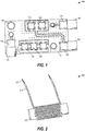
- FIG. 1 is an overhead view of a cryogenic RF resonator circuit board 100, according to an embodiment.
- Circuit board 100 may include mounting holes 105 and 110 for fixing the circuit board 100 to an enclosure.
- Circuit board 100 may include various RF input and output ports, such as RF input port 150, RF input mount 145, output port 155, and RF output mount 125.
- Circuit board 100 may include an integrated voltage pick-off circuit, which may be used to monitor a voltage gain.
- the voltage pick-off circuit includes surface mount components 115 and 120, along with voltage pick-off port 160 and voltage pick-off mount 130.
- Circuit board 100 may include various circuit components to modify an input RF signal received at the RF input port 155, such as capacitors 135 and 140. These capacitors may be coupled with one or more inductors, such as shown in FIG. 2 .
- FIG. 2 is an overhead view of a cryogenic RF resonator inductor 200, according to an embodiment.
- Inductor 200 may include a conductive wire 205 within an insulating sheath 210.
- the wire 205 and sheath 210 may be wound around a dielectric core 215.
- the dielectric used in the dielectric core 215 may be selected to provide mechanical stability for the inductor coil and a desired dielectric constant.
- the dielectric core 215 and capacitors 135 and 140 may include materials to provide consistent dielectric properties (e.g., a narrow range of dielectric constant values) within cryogenic operating conditions, such as between approximately 4 Kelvin and approximately 77 Kelvin.
- the dielectric materials and other materials used for components of the inductor 200 and the circuit board 100 may be selected to provide stable characteristics over temperature, voltage, and RF frequency ranges used in operation of cryogenic ion traps.
- the impedance of inductor 200 and capacitance of capacitors 135 and 140 may be selected to form an impedance-matching circuit, such as in an L-network formation.
- a network analyzer may be used to determine the real and imaginary parts of impedance of an ion trap, and the impedance of inductor 200 and capacitance of capacitors 135 and 140 may be selected to match the ion trap impedance.
- the real part of the ion trap impedance and the real part of the cryogenic resonator impedance is expected to change as the operating temperature is decreased.
- multiple impedance measurements may be taken as the device is cooled, and the multiple impedance measurements may be used to extrapolate impedance values for the ion trap at various operating temperatures. Based on the measured and extrapolated impedance values for the ion trap at various operating temperatures, the impedance of inductor 200 and capacitance of capacitors 135 and 140 may be selected to match the ion trap impedance.
- FIG. 3 is a perspective view of a cryogenic RF resonator open enclosure 300, according to an embodiment.
- the open enclosure may include a cavity into which the inductor is placed with inductor contacts 390 exposed.
- the cavity may be filled with a thermally conductive substrate 380 such as epoxy.
- the substrate 380 may ensure the inductor is stabilized relative to the enclosure 300, and the thermal conductivity of the substrate 380 may be selected to conduct heat away from the inductor to the enclosure 300, which in turn conducts heat away to the cryogenic cooling system.
- Enclosure 300 may be formed from materials that are thermally conductive and operate at cryogenic application temperatures. Enclosure 300 may include a high-purity copper, such as oxygen-free high thermal conductivity (OFHC) copper. Enclosure 300 may include a thermally conductive external gold plating, such as on outer surface 385. Enclosure 300 may include mounting surfaces 370 and 375, which may be used to position the circuit board. Enclosure 300 may include threaded mounting aperture, such as threaded aperture 365 that may be used with a bolt or other fastener through circuit board aperture 305.
- OFHC oxygen-free high thermal conductivity
- FIG. 4 is a top view of a cryogenic RF resonator open enclosure 400, according to an embodiment.
- Enclosure 400 may include a cryogenic RF resonator circuit board, which may be fastened to enclosure 400 through board apertures 405 and 410.
- Inductor leads 490 may be routed from an inductor to corresponding contacts on the circuit board.
- a thermally conductive substrate 380 may be used to cover inductor leads 490, such as to provide structural stability and thermal conductivity.
- One or more of the circuit board components 415 and 420 may be covered partially or completely with substrate 380 to further improve structural stability and thermal conductivity.
- Other circuit board components 435, 440, and 465 may be left uncovered by substrate 380, such as to provide a user-modifiable impedance.
- components 435, 440, and 465 may include capacitors of common or different capacitance, and one or more of components 435, 440, and 465 may be removed or replaced with a different component.
- components 435, 440, and 465 may be replaced by a user-adjustable variable capacitor. This selection or modification of components 435, 440, and 465 may provide a desired capacitance, which may be used to modify the cryogenic RF resonator to provide an impedance that matches an ion trap.
- FIG. 5 is a perspective view of a cryogenic RF resonator closed enclosure 500, according to an embodiment.
- Enclosure 500 includes a thermally conductive lower enclosure 585 and a thermally conductive upper surface 595, which may be fastened together using a bolt or other fastener 590.
- the closed enclosure 500 may include apertures, such as for RF output port 555 connecting the resonator with the ion trap, RF input port 550, or voltage pick-off port 560.
- cryogenic RF resonator within enclosure 500 may be used to verify the cryogenic RF resonator is impedance-matched to an ion trap.
- cryogenic RF resonator may be connected to an ion trap, the cryogenic RF resonator and ion trap may be cooled to a low cryogenic temperature (e.g., 4 Kelvin), and a network analyzer may be used to measure power reflected back from the ion trap. This measured power may be used to determine an internal quality factor (e.g., resonator loss measurement), which may be used to verify that the cryogenic RF resonator is properly impedance-matched to ion trap.
- a low cryogenic temperature e.g. 4 Kelvin
- FIG. 6 is a block diagram of a cryogenic RF resonator method 600, according to an embodiment.
- Method 600 may include receiving 610 an input radio-frequency (RF) signal via an RF input port at a cryogenic resonant circuit.
- the cryogenic resonant circuit may include an inductive device disposed at least partially within a thermally conductive substrate and a cryogenic capacitive device coupled to the inductor.
- Method 600 may include generating 620 an impedance-matched RF signal at the cryogenic resonant circuit based on the input RF signal.
- Method 600 may include providing 630 the impedance-matched RF signal via an RF output port to an external cryogenic device.
- the cryogenic resonant circuit serves as an amplifier circuit.
- the generation of the impedance-matched RF signal at the cryogenic resonant circuit may include generating an impedance-matched amplified RF signal.
- the provision of the impedance-matched RF signal may include providing the impedance-matched amplified RF signal to the external cryogenic device.
- the cryogenic resonant circuit may be disposed within a thermally conductive enclosure.
- the thermally conductive enclosure may include a thermally conductive high-purity copper.
- the thermally conductive enclosure may include a thermally conductive gold plating.
- the thermally conductive enclosure may include at least one thermally conductive surface configured to mate with a thermally conductive mounting substrate.
- the cryogenic capacitive device may be configured to provide an adjustable capacitance, where the capacitance may be adjusted based on the user input or based on other changes.
- method 600 may include receiving 640 a user-selectable capacitance input to provide the adjustable capacitance, where the user-selectable capacitance may include a user adjustment to a variable capacitor.
- the cryogenic capacitive device may include a plurality of conductors, and each of the plurality of capacitors may be configured to be removable by a user to provide the adjustable capacitance.
- the capacitance may be adjusted to provide a desired impedance, such as to provide a desired impedance value.
- the cryogenic capacitive device may include materials to provide consistent dielectric properties and to provide other stable characteristics over temperature, voltage, and RF frequency ranges used in operation of cryogenic ion traps.
- Example 1 is a cryogenic radio-frequency resonator system comprising: an inductive device disposed at least partially within a thermally conductive substrate; a cryogenic capacitive device coupled to the inductor to form a cryogenic resonant circuit with an associated circuit impedance value; a radio-frequency (RF) input port to route an input RF signal to the cryogenic resonant circuit, the cryogenic resonant circuit generating an impedance-matched RF signal; and an RF output port to provide the impedance-matched RF signal to an external cryogenic device.
- RF radio-frequency
- Example 2 the subject matter of Example 1 optionally includes wherein: the cryogenic resonant circuit includes an amplifier circuit; the amplifier circuit generates an impedance-matched amplified RF signal; and the RF output port provides the impedance-matched amplified RF signal to the external cryogenic device.
- Example 3 the subject matter of any one or more of Examples 1-2 optionally include a thermally conductive enclosure.
- Example 4 the subject matter of Example 3 optionally includes wherein the thermally conductive enclosure includes a thermally conductive high-purity copper.
- Example 5 the subject matter of any one or more of Examples 3-4 optionally include wherein the thermally conductive enclosure includes a thermally conductive gold plating.
- Example 6 the subject matter of any one or more of Examples 3-5 optionally include wherein the thermally conductive enclosure includes at least one thermally conductive surface configured to mate with a thermally conductive mounting substrate.
- Example 7 the subject matter of any one or more of Examples 1-6 optionally include wherein the cryogenic capacitive device includes a low-temperature capacitive material.
- Example 8 the subject matter of any one or more of Examples 1-7 optionally include wherein the cryogenic capacitive device is configured to provide an adjustable capacitance, the adjustable capacitance modifying the amplifier impedance.
- Example 9 the subject matter of Example 8 optionally includes wherein the cryogenic capacitive device includes a plurality of conductors, each of the plurality of capacitors configured to be removable to provide the adjustable capacitance.
- Example 10 the subject matter of any one or more of Examples 8-9 optionally include wherein the cryogenic capacitive device includes a user-selectable capacitance to provide the adjustable capacitance.
- Example 11 is a cryogenic radio-frequency resonator method comprising: receiving an input radio-frequency (RF) signal via an RF input port at a cryogenic resonant circuit, the cryogenic resonant circuit including an inductive device disposed at least partially within a thermally conductive substrate and a cryogenic capacitive device coupled to the inductor; generating an impedance-matched RF signal at the cryogenic resonant circuit based on the input RF signal; and providing the impedance-matched RF signal via an RF output port to an external cryogenic device.
- RF radio-frequency
- Example 12 the subject matter of Example 11 optionally includes wherein: the cryogenic resonant circuit includes an amplifier circuit; the generation of the impedance-matched RF signal at the cryogenic resonant circuit includes generating an impedance-matched amplified RF signal; and the provision of the impedance-matched RF signal includes providing the impedance-matched amplified RF signal to the external cryogenic device.
- Example 13 the subject matter of any one or more of Examples 11-12 optionally include wherein the cryogenic resonant circuit is disposed within a thermally conductive enclosure.
- Example 14 the subject matter of Example 13 optionally includes wherein the thermally conductive enclosure includes a thermally conductive high-purity copper.
- Example 15 the subject matter of any one or more of Examples 13-14 optionally include wherein the thermally conductive enclosure includes a thermally conductive gold plating.
- Example 16 the subject matter of any one or more of Examples 13-15 optionally include wherein the thermally conductive enclosure includes at least one thermally conductive surface configured to mate with a thermally conductive mounting substrate.
- Example 17 the subject matter of any one or more of Examples 11-16 optionally include wherein the cryogenic capacitive device includes a low-temperature capacitive material.
- Example 18 the subject matter of any one or more of Examples 11-17 optionally include wherein the cryogenic capacitive device is configured to provide an adjustable capacitance, the adjustable capacitance modifying the amplifier impedance.
- Example 19 the subject matter of Example 18 optionally includes wherein the cryogenic capacitive device includes a plurality of conductors, each of the plurality of capacitors configured to be removable to provide the adjustable capacitance.
- Example 20 the subject matter of any one or more of Examples 18-19 optionally include receiving a user-selectable capacitance input to provide the adjustable capacitance.
- Example 21 is one or more machine-readable medium including instructions, which when executed by a computing system, cause the computing system to perform any of the methods of Examples 11-20.
- Example 22 is an apparatus comprising means for performing any of the methods of Examples 11-20.
- Example 23 is a machine-readable storage medium comprising a plurality of instructions that, when executed with a processor of a device, cause the device to: receive an input radio-frequency (RF) signal via an RF input port at a cryogenic resonant circuit, the cryogenic resonant circuit including an inductive device disposed at least partially within a thermally conductive substrate and a cryogenic capacitive device coupled to the inductor; generate an impedance-matched RF signal at the cryogenic resonant circuit based on the input RF signal; and provide the impedance-matched RF signal via an RF output port to an external cryogenic device.
- RF radio-frequency
- Example 24 the subject matter of Example 23 optionally includes wherein: the cryogenic resonant circuit includes an amplifier circuit; the instructions further causing the device to generate an impedance-matched amplified RF signal; and the instructions further causing the device to provide the impedance-matched amplified RF signal to the external cryogenic device.
- Example 25 the subject matter of any one or more of Examples 23-24 optionally include wherein the cryogenic resonant circuit is disposed within a thermally conductive enclosure.
- Example 26 the subject matter of Example 25 optionally includes wherein the thermally conductive enclosure includes a thermally conductive high-purity copper.
- Example 27 the subject matter of any one or more of Examples 25-26 optionally include wherein the thermally conductive enclosure includes a thermally conductive gold plating.
- Example 28 the subject matter of any one or more of Examples 25-27 optionally include wherein the thermally conductive enclosure includes at least one thermally conductive surface configured to mate with a thermally conductive mounting substrate.
- Example 29 the subject matter of any one or more of Examples 23-28 optionally include wherein the cryogenic capacitive device includes a low-temperature capacitive material.
- Example 30 the subject matter of any one or more of Examples 23-29 optionally include wherein the cryogenic capacitive device is configured to provide an adjustable capacitance, the adjustable capacitance modifying the amplifier impedance.
- Example 31 the subject matter of Example 30 optionally includes wherein the cryogenic capacitive device includes a plurality of conductors, each of the plurality of capacitors configured to be removable to provide the adjustable capacitance.
- Example 32 the subject matter of any one or more of Examples 30-31 optionally include the instructions further causing the device to receive a user-selectable capacitance input to provide the adjustable capacitance.
- Example 33 is a cryogenic radio-frequency resonator apparatus comprising: means for receiving an input radio-frequency (RF) signal via an RF input port at a cryogenic resonant circuit, the cryogenic resonant circuit including an inductive device disposed at least partially within a thermally conductive substrate and a cryogenic capacitive device coupled to the inductor; means for generating an impedance-matched RF signal at the cryogenic resonant circuit based on the input RF signal; and means for providing the impedance-matched RF signal via an RF output port to an external cryogenic device.
- RF radio-frequency
- Example 34 the subject matter of Example 33 optionally includes wherein: the cryogenic resonant circuit includes an amplifier circuit; the generation of the impedance-matched RF signal at the cryogenic resonant circuit includes means for generating an impedance-matched amplified RF signal; and the provision of the impedance-matched RF signal includes means for providing the impedance-matched amplified RF signal to the external cryogenic device.
- Example 35 the subject matter of any one or more of Examples 33-34 optionally include wherein the cryogenic resonant circuit is disposed within a thermally conductive enclosure.
- Example 36 the subject matter of Example 35 optionally includes wherein the thermally conductive enclosure includes a thermally conductive high-purity copper.
- Example 37 the subject matter of any one or more of Examples 35-36 optionally include wherein the thermally conductive enclosure includes a thermally conductive gold plating.
- Example 38 the subject matter of any one or more of Examples 35-37 optionally include wherein the thermally conductive enclosure includes at least one thermally conductive surface configured to mate with a thermally conductive mounting substrate.
- Example 39 the subject matter of any one or more of Examples 33-38 optionally include wherein the cryogenic capacitive device includes a low-temperature capacitive material.
- Example 40 the subject matter of any one or more of Examples 33-39 optionally include wherein the cryogenic capacitive device is configured to provide an adjustable capacitance, the adjustable capacitance modifying the amplifier impedance.
- Example 41 the subject matter of Example 40 optionally includes wherein the cryogenic capacitive device includes a plurality of conductors, each of the plurality of capacitors configured to be removable to provide the adjustable capacitance.
- Example 42 the subject matter of any one or more of Examples 40-41 optionally include means for receiving a user-selectable capacitance input to provide the adjustable capacitance.
- Example 43 is one or more machine-readable medium including instructions, which when executed by a machine, cause the machine to perform operations of any of the operations of Examples 1-42.
- Example 44 is an apparatus comprising means for performing any of the operations of Examples 1-42.
- Example 45 is a system to perform the operations of any of the Examples 1-42.
- Example 46 is a method to perform the operations of any of the Examples 1-42.
Landscapes
- Physics & Mathematics (AREA)
- Acoustics & Sound (AREA)
- Engineering & Computer Science (AREA)
- Power Engineering (AREA)
- General Physics & Mathematics (AREA)
- Amplifiers (AREA)
- Filters And Equalizers (AREA)
- Cooling Or The Like Of Electrical Apparatus (AREA)
- Microwave Amplifiers (AREA)
- Magnetic Resonance Imaging Apparatus (AREA)
Abstract
Description
- Embodiments described herein generally relate to quantum computing applications.
- Cryogenic ion traps (e.g., surface ion traps) are an emerging technology that enable the confinement of ions for applications in quantum computing, quantum sensing, quantum timing, and other applications in quantum technology. During operation, these ion traps use input radio-frequency drive signals at relatively high voltages. However, operating such ion traps at cryogenic temperatures may result in unwanted power dissipation. What is needed is an improved solution to increase the efficiency of a cryogenic ion trap system.
-
-
FIG. 1 is an overhead view of a cryogenic RF resonator circuit board, according to an embodiment. -
FIG. 2 is an overhead view of a cryogenic RF resonator inductor, according to an embodiment. -
FIG. 3 is a perspective view of a cryogenic RF resonator open enclosure, according to an embodiment. -
FIG. 4 is a top view of a cryogenic RF resonator open enclosure, according to an embodiment. -
FIG. 5 is a perspective view of a cryogenic RF resonator closed enclosure, according to an embodiment. -
FIG. 6 is a block diagram of a cryogenic RF resonator method, according to an embodiment. - The present subject matter provides technical solutions for the technical problems facing cryogenic ion traps by providing a cryogenic radio-frequency (RF) resonator that is compact, monolithic, modular, and impedance-matched to a cryogenic ion trap. The cryogenic RF resonator described herein is power-efficient, properly impedance-matched to the RF source, has a stable gain profile, and is compatible with a low temperature and ultra-high vacuum environment. In some examples, the gain profile is selected so that the cryogenic RF resonator acts as a cryogenic RF amplifier. This cryogenic RF resonator improves the performance of ion traps by reducing or minimizing the heat load and reducing or minimizing the unwanted noise that may erroneously drive trapped ions. These features of the present subject matter improve the performance of atomic clocks and mass spectrometers, and especially improve the performance of quantum computing. In an example, a cryogenic RF resonator and ion trap package may be used to store quantum information using qubits (e.g., stable electronic states of ions), and quantum information can be processed and transferred through the collective quantized motion of the ions. One or more ion-specific lasers may be applied to the ions to induce coupling of the ions between qubit states or to induce coupling between internal qubit states and external motional states.
- The cryogenic RF resonator described herein provides various advantages. The cryogenic RF resonator may dissipate reduced power inside a cryostat (e.g., cryogenic chamber), such as power levels of approximately 100 mW or lower. This reduces the power required to operate the cryostat, especially for cryostats operated from approximately 4 Kelvin to approximately 77 Kelvin. The cryogenic RF resonator may provide a gain profile that provides state-of-the-art stability without the use of active feedback in a circuit. As described below, selection of capacitance and inductance values may provide a desired gain profile without the need for active feedback within the circuit. The cryogenic RF resonator may provide a compact and modular form factor. This enables the use of this cryogenic RF resonator with various ion traps. The cryogenic RF resonator may provide an integrated voltage pick-off circuit. If the cryogenic RF resonator is used as an amplifier, this voltage pick-off circuit may be used to monitor a voltage gain of the amplifier.
- The cryogenic RF resonator described herein provides various advantages over other RF resonators. In an example, the cryogenic RF resonator provides an RF output that is impedance-matched to an RF source. In an example, this cryogenic RF resonator provides an improved design, including a form factor that is compact, modular, and monolithic (e.g., substantially solid and uniform). Some RF resonators may be implemented using bulky helical resonators or using discrete components mounted directly to ion trap circuit boards. However, because those RF resonators are not monolithic, they are sensitive to mechanical vibrations that degrade the stability of the circuit gain profile. In contrast, this cryogenic RF resonator includes a formed substrate (e.g., epoxy) to provide a monolithic circuit that reduces or eliminates susceptibility to mechanical vibrations. This cryogenic RF resonator is also compact and modular, which provides the ability to use this cryogenic RF resonator for providing impedance-matched RF signals to various ion trap devices.
- The following description and the drawings sufficiently illustrate specific embodiments to enable those skilled in the art to understand the specific embodiment. Other embodiments may incorporate structural, logical, electrical, process, and other changes. Portions and features of various embodiments may be included in, or substituted for, those of other embodiments. Embodiments set forth in the claims encompass all available equivalents of those claims.
-
FIG. 1 is an overhead view of a cryogenic RFresonator circuit board 100, according to an embodiment.Circuit board 100 may includemounting holes circuit board 100 to an enclosure.Circuit board 100 may include various RF input and output ports, such asRF input port 150,RF input mount 145,output port 155, andRF output mount 125.Circuit board 100 may include an integrated voltage pick-off circuit, which may be used to monitor a voltage gain. In an example, the voltage pick-off circuit includessurface mount components off port 160 and voltage pick-off mount 130.Circuit board 100 may include various circuit components to modify an input RF signal received at theRF input port 155, such ascapacitors FIG. 2 . -
FIG. 2 is an overhead view of a cryogenicRF resonator inductor 200, according to an embodiment.Inductor 200 may include a conductive wire 205 within aninsulating sheath 210. The wire 205 andsheath 210 may be wound around adielectric core 215. The dielectric used in thedielectric core 215 may be selected to provide mechanical stability for the inductor coil and a desired dielectric constant. For example, thedielectric core 215 andcapacitors inductor 200 and thecircuit board 100 may be selected to provide stable characteristics over temperature, voltage, and RF frequency ranges used in operation of cryogenic ion traps. - The impedance of
inductor 200 and capacitance ofcapacitors inductor 200 and capacitance ofcapacitors inductor 200 and capacitance ofcapacitors -
FIG. 3 is a perspective view of a cryogenic RF resonatoropen enclosure 300, according to an embodiment. The open enclosure may include a cavity into which the inductor is placed withinductor contacts 390 exposed. The cavity may be filled with a thermallyconductive substrate 380 such as epoxy. Thesubstrate 380 may ensure the inductor is stabilized relative to theenclosure 300, and the thermal conductivity of thesubstrate 380 may be selected to conduct heat away from the inductor to theenclosure 300, which in turn conducts heat away to the cryogenic cooling system. -
Enclosure 300 may be formed from materials that are thermally conductive and operate at cryogenic application temperatures.Enclosure 300 may include a high-purity copper, such as oxygen-free high thermal conductivity (OFHC) copper.Enclosure 300 may include a thermally conductive external gold plating, such as onouter surface 385.Enclosure 300 may include mountingsurfaces Enclosure 300 may include threaded mounting aperture, such as threadedaperture 365 that may be used with a bolt or other fastener throughcircuit board aperture 305. -
FIG. 4 is a top view of a cryogenic RF resonatoropen enclosure 400, according to an embodiment.Enclosure 400 may include a cryogenic RF resonator circuit board, which may be fastened toenclosure 400 throughboard apertures conductive substrate 380 may be used to cover inductor leads 490, such as to provide structural stability and thermal conductivity. One or more of thecircuit board components substrate 380 to further improve structural stability and thermal conductivity. Othercircuit board components substrate 380, such as to provide a user-modifiable impedance. For example,components components components components -
FIG. 5 is a perspective view of a cryogenic RF resonator closedenclosure 500, according to an embodiment.Enclosure 500 includes a thermally conductivelower enclosure 585 and a thermally conductiveupper surface 595, which may be fastened together using a bolt orother fastener 590. Theclosed enclosure 500 may include apertures, such as forRF output port 555 connecting the resonator with the ion trap,RF input port 550, or voltage pick-offport 560. - In operation, the cryogenic RF resonator within
enclosure 500 may be used to verify the cryogenic RF resonator is impedance-matched to an ion trap. For example, cryogenic RF resonator may be connected to an ion trap, the cryogenic RF resonator and ion trap may be cooled to a low cryogenic temperature (e.g., 4 Kelvin), and a network analyzer may be used to measure power reflected back from the ion trap. This measured power may be used to determine an internal quality factor (e.g., resonator loss measurement), which may be used to verify that the cryogenic RF resonator is properly impedance-matched to ion trap. -
FIG. 6 is a block diagram of a cryogenicRF resonator method 600, according to an embodiment.Method 600 may include receiving 610 an input radio-frequency (RF) signal via an RF input port at a cryogenic resonant circuit. The cryogenic resonant circuit may include an inductive device disposed at least partially within a thermally conductive substrate and a cryogenic capacitive device coupled to the inductor.Method 600 may include generating 620 an impedance-matched RF signal at the cryogenic resonant circuit based on the input RF signal.Method 600 may include providing 630 the impedance-matched RF signal via an RF output port to an external cryogenic device. - In an example, the cryogenic resonant circuit serves as an amplifier circuit. The generation of the impedance-matched RF signal at the cryogenic resonant circuit may include generating an impedance-matched amplified RF signal. The provision of the impedance-matched RF signal may include providing the impedance-matched amplified RF signal to the external cryogenic device.
- The cryogenic resonant circuit may be disposed within a thermally conductive enclosure. The thermally conductive enclosure may include a thermally conductive high-purity copper. The thermally conductive enclosure may include a thermally conductive gold plating. The thermally conductive enclosure may include at least one thermally conductive surface configured to mate with a thermally conductive mounting substrate.
- The cryogenic capacitive device may be configured to provide an adjustable capacitance, where the capacitance may be adjusted based on the user input or based on other changes. In an example,
method 600 may include receiving 640 a user-selectable capacitance input to provide the adjustable capacitance, where the user-selectable capacitance may include a user adjustment to a variable capacitor. In an example, the cryogenic capacitive device may include a plurality of conductors, and each of the plurality of capacitors may be configured to be removable by a user to provide the adjustable capacitance. The capacitance may be adjusted to provide a desired impedance, such as to provide a desired impedance value. In an example, the cryogenic capacitive device may include materials to provide consistent dielectric properties and to provide other stable characteristics over temperature, voltage, and RF frequency ranges used in operation of cryogenic ion traps. - The above detailed description includes references to the accompanying drawings, which form a part of the detailed description. The drawings show, by way of illustration, specific embodiments in which the invention can be practiced. These embodiments are also referred to herein as "examples." Such examples can include elements in addition to those shown or described. However, the present inventors also contemplate examples in which only those elements shown or described are provided. Moreover, the present inventors also contemplate examples using any combination or permutation of those elements shown or described (or one or more aspects thereof), either with respect to a particular example (or one or more aspects thereof), or with respect to other examples (or one or more aspects thereof) shown or described herein.
- Example 1 is a cryogenic radio-frequency resonator system comprising: an inductive device disposed at least partially within a thermally conductive substrate; a cryogenic capacitive device coupled to the inductor to form a cryogenic resonant circuit with an associated circuit impedance value; a radio-frequency (RF) input port to route an input RF signal to the cryogenic resonant circuit, the cryogenic resonant circuit generating an impedance-matched RF signal; and an RF output port to provide the impedance-matched RF signal to an external cryogenic device.
- In Example 2, the subject matter of Example 1 optionally includes wherein: the cryogenic resonant circuit includes an amplifier circuit; the amplifier circuit generates an impedance-matched amplified RF signal; and the RF output port provides the impedance-matched amplified RF signal to the external cryogenic device.
- In Example 3, the subject matter of any one or more of Examples 1-2 optionally include a thermally conductive enclosure.
- In Example 4, the subject matter of Example 3 optionally includes wherein the thermally conductive enclosure includes a thermally conductive high-purity copper.
- In Example 5, the subject matter of any one or more of Examples 3-4 optionally include wherein the thermally conductive enclosure includes a thermally conductive gold plating.
- In Example 6, the subject matter of any one or more of Examples 3-5 optionally include wherein the thermally conductive enclosure includes at least one thermally conductive surface configured to mate with a thermally conductive mounting substrate.
- In Example 7, the subject matter of any one or more of Examples 1-6 optionally include wherein the cryogenic capacitive device includes a low-temperature capacitive material.
- In Example 8, the subject matter of any one or more of Examples 1-7 optionally include wherein the cryogenic capacitive device is configured to provide an adjustable capacitance, the adjustable capacitance modifying the amplifier impedance.
- In Example 9, the subject matter of Example 8 optionally includes wherein the cryogenic capacitive device includes a plurality of conductors, each of the plurality of capacitors configured to be removable to provide the adjustable capacitance.
- In Example 10, the subject matter of any one or more of Examples 8-9 optionally include wherein the cryogenic capacitive device includes a user-selectable capacitance to provide the adjustable capacitance.
- Example 11 is a cryogenic radio-frequency resonator method comprising: receiving an input radio-frequency (RF) signal via an RF input port at a cryogenic resonant circuit, the cryogenic resonant circuit including an inductive device disposed at least partially within a thermally conductive substrate and a cryogenic capacitive device coupled to the inductor; generating an impedance-matched RF signal at the cryogenic resonant circuit based on the input RF signal; and providing the impedance-matched RF signal via an RF output port to an external cryogenic device.
- In Example 12, the subject matter of Example 11 optionally includes wherein: the cryogenic resonant circuit includes an amplifier circuit; the generation of the impedance-matched RF signal at the cryogenic resonant circuit includes generating an impedance-matched amplified RF signal; and the provision of the impedance-matched RF signal includes providing the impedance-matched amplified RF signal to the external cryogenic device.
- In Example 13, the subject matter of any one or more of Examples 11-12 optionally include wherein the cryogenic resonant circuit is disposed within a thermally conductive enclosure.
- In Example 14, the subject matter of Example 13 optionally includes wherein the thermally conductive enclosure includes a thermally conductive high-purity copper.
- In Example 15, the subject matter of any one or more of Examples 13-14 optionally include wherein the thermally conductive enclosure includes a thermally conductive gold plating.
- In Example 16, the subject matter of any one or more of Examples 13-15 optionally include wherein the thermally conductive enclosure includes at least one thermally conductive surface configured to mate with a thermally conductive mounting substrate.
- In Example 17, the subject matter of any one or more of Examples 11-16 optionally include wherein the cryogenic capacitive device includes a low-temperature capacitive material.
- In Example 18, the subject matter of any one or more of Examples 11-17 optionally include wherein the cryogenic capacitive device is configured to provide an adjustable capacitance, the adjustable capacitance modifying the amplifier impedance.
- In Example 19, the subject matter of Example 18 optionally includes wherein the cryogenic capacitive device includes a plurality of conductors, each of the plurality of capacitors configured to be removable to provide the adjustable capacitance.
- In Example 20, the subject matter of any one or more of Examples 18-19 optionally include receiving a user-selectable capacitance input to provide the adjustable capacitance.
- Example 21 is one or more machine-readable medium including instructions, which when executed by a computing system, cause the computing system to perform any of the methods of Examples 11-20.
- Example 22 is an apparatus comprising means for performing any of the methods of Examples 11-20.
- Example 23 is a machine-readable storage medium comprising a plurality of instructions that, when executed with a processor of a device, cause the device to: receive an input radio-frequency (RF) signal via an RF input port at a cryogenic resonant circuit, the cryogenic resonant circuit including an inductive device disposed at least partially within a thermally conductive substrate and a cryogenic capacitive device coupled to the inductor; generate an impedance-matched RF signal at the cryogenic resonant circuit based on the input RF signal; and provide the impedance-matched RF signal via an RF output port to an external cryogenic device.
- In Example 24, the subject matter of Example 23 optionally includes wherein: the cryogenic resonant circuit includes an amplifier circuit; the instructions further causing the device to generate an impedance-matched amplified RF signal; and the instructions further causing the device to provide the impedance-matched amplified RF signal to the external cryogenic device.
- In Example 25, the subject matter of any one or more of Examples 23-24 optionally include wherein the cryogenic resonant circuit is disposed within a thermally conductive enclosure.
- In Example 26, the subject matter of Example 25 optionally includes wherein the thermally conductive enclosure includes a thermally conductive high-purity copper.
- In Example 27, the subject matter of any one or more of Examples 25-26 optionally include wherein the thermally conductive enclosure includes a thermally conductive gold plating.
- In Example 28, the subject matter of any one or more of Examples 25-27 optionally include wherein the thermally conductive enclosure includes at least one thermally conductive surface configured to mate with a thermally conductive mounting substrate.
- In Example 29, the subject matter of any one or more of Examples 23-28 optionally include wherein the cryogenic capacitive device includes a low-temperature capacitive material.
- In Example 30, the subject matter of any one or more of Examples 23-29 optionally include wherein the cryogenic capacitive device is configured to provide an adjustable capacitance, the adjustable capacitance modifying the amplifier impedance.
- In Example 31, the subject matter of Example 30 optionally includes wherein the cryogenic capacitive device includes a plurality of conductors, each of the plurality of capacitors configured to be removable to provide the adjustable capacitance.
- In Example 32, the subject matter of any one or more of Examples 30-31 optionally include the instructions further causing the device to receive a user-selectable capacitance input to provide the adjustable capacitance.
- Example 33 is a cryogenic radio-frequency resonator apparatus comprising: means for receiving an input radio-frequency (RF) signal via an RF input port at a cryogenic resonant circuit, the cryogenic resonant circuit including an inductive device disposed at least partially within a thermally conductive substrate and a cryogenic capacitive device coupled to the inductor; means for generating an impedance-matched RF signal at the cryogenic resonant circuit based on the input RF signal; and means for providing the impedance-matched RF signal via an RF output port to an external cryogenic device.
- In Example 34, the subject matter of Example 33 optionally includes wherein: the cryogenic resonant circuit includes an amplifier circuit; the generation of the impedance-matched RF signal at the cryogenic resonant circuit includes means for generating an impedance-matched amplified RF signal; and the provision of the impedance-matched RF signal includes means for providing the impedance-matched amplified RF signal to the external cryogenic device.
- In Example 35, the subject matter of any one or more of Examples 33-34 optionally include wherein the cryogenic resonant circuit is disposed within a thermally conductive enclosure.
- In Example 36, the subject matter of Example 35 optionally includes wherein the thermally conductive enclosure includes a thermally conductive high-purity copper.
- In Example 37, the subject matter of any one or more of Examples 35-36 optionally include wherein the thermally conductive enclosure includes a thermally conductive gold plating.
- In Example 38, the subject matter of any one or more of Examples 35-37 optionally include wherein the thermally conductive enclosure includes at least one thermally conductive surface configured to mate with a thermally conductive mounting substrate.
- In Example 39, the subject matter of any one or more of Examples 33-38 optionally include wherein the cryogenic capacitive device includes a low-temperature capacitive material.
- In Example 40, the subject matter of any one or more of Examples 33-39 optionally include wherein the cryogenic capacitive device is configured to provide an adjustable capacitance, the adjustable capacitance modifying the amplifier impedance.
- In Example 41, the subject matter of Example 40 optionally includes wherein the cryogenic capacitive device includes a plurality of conductors, each of the plurality of capacitors configured to be removable to provide the adjustable capacitance.
- In Example 42, the subject matter of any one or more of Examples 40-41 optionally include means for receiving a user-selectable capacitance input to provide the adjustable capacitance.
- Example 43 is one or more machine-readable medium including instructions, which when executed by a machine, cause the machine to perform operations of any of the operations of Examples 1-42.
- Example 44 is an apparatus comprising means for performing any of the operations of Examples 1-42.
- Example 45 is a system to perform the operations of any of the Examples 1-42.
- Example 46 is a method to perform the operations of any of the Examples 1-42.
- In this document, the terms "a" or "an" are used, as is common in patent documents, to include one or more than one, independent of any other instances or usages of "at least one" or "one or more." In this document, the term "or" is used to refer to a nonexclusive or, such that "A or B" includes "A but not B," "B but not A," and "A and B," unless otherwise indicated. In this document, the terms "including" and "in which" are used as the plain-English equivalents of the respective terms "comprising" and "wherein." Also, in the following claims, the terms "including" and "comprising" are open-ended, that is, a system, device, article, composition, formulation, or process that includes elements in addition to those listed after such a term in a claim are still deemed to fall within the scope of that claim. Moreover, in the following claims, the terms "first," "second," and "third," etc. are used merely as labels, and are not intended to impose numerical requirements on their objects.
- The above description is intended to be illustrative, and not restrictive. For example, the above-described examples (or one or more aspects thereof) may be used in combination with each other. Other embodiments can be used, such as by one of ordinary skill in the art upon reviewing the above description. The Abstract is provided to allow the reader to quickly ascertain the nature of the technical disclosure. It is submitted with the understanding that it will not be used to interpret or limit the scope or meaning of the claims. In the above Detailed Description, various features may be grouped together to streamline the disclosure. This should not be interpreted as intending that an unclaimed disclosed feature is essential to any claim. Rather, inventive subject matter may lie in less than all features of a particular disclosed embodiment. Thus, the following claims are hereby incorporated into the Detailed Description, with each claim standing on its own as a separate embodiment, and it is contemplated that such embodiments can be combined with each other in various combinations or permutations. The scope should be determined with reference to the appended claims, along with the full scope of equivalents to which such claims are entitled.
Claims (15)
- A cryogenic radio-frequency resonator system comprising:an inductive device disposed at least partially within a thermally conductive substrate;a cryogenic capacitive device coupled to the inductor to form a cryogenic resonant circuit with an associated circuit impedance value;a radio-frequency (RF) input port to route an input RF signal to the cryogenic resonant circuit, the cryogenic resonant circuit generating an impedance-matched RF signal; andan RF output port to provide the impedance-matched RF signal to an external cryogenic device.
- The system of claim 1, wherein:the cryogenic resonant circuit includes an amplifier circuit;the amplifier circuit generates an impedance-matched amplified RF signal; andthe RF output port provides the impedance-matched amplified RF signal to the external cryogenic device.
- The system of claim 1, further including a thermally conductive enclosure.
- The system of claim 3, wherein the thermally conductive enclosure includes a thermally conductive high-purity copper.
- The system of claim 3, wherein the thermally conductive enclosure includes at least one thermally conductive surface configured to mate with a thermally conductive mounting substrate.
- The system of claim 1, wherein the cryogenic capacitive device includes a low-temperature capacitive material.
- The system of claim 1, wherein the cryogenic capacitive device is configured to provide an adjustable capacitance, the adjustable capacitance modifying the amplifier impedance.
- The system of claim 7, wherein the cryogenic capacitive device includes a plurality of conductors, each of the plurality of capacitors configured to be removable to provide the adjustable capacitance.
- A cryogenic radio-frequency resonator method comprising:receiving an input radio-frequency (RF) signal via an RF input port at a cryogenic resonant circuit, the cryogenic resonant circuit including an inductive device disposed at least partially within a thermally conductive substrate and a cryogenic capacitive device coupled to the inductor;generating an impedance-matched RF signal at the cryogenic resonant circuit based on the input RF signal; andproviding the impedance-matched RF signal via an RF output port to an external cryogenic device.
- The method of claim 9, wherein:the cryogenic resonant circuit includes an amplifier circuit;the generation of the impedance-matched RF signal at the cryogenic resonant circuit includes generating an impedance-matched amplified RF signal; andthe provision of the impedance-matched RF signal includes providing the impedance-matched amplified RF signal to the external cryogenic device.
- The method of claim 9, wherein the cryogenic resonant circuit is disposed within a thermally conductive enclosure.
- The method of claim 11, wherein the thermally conductive enclosure includes a thermally conductive high-purity copper.
- The method of claim 11, wherein the thermally conductive enclosure includes at least one thermally conductive surface configured to mate with a thermally conductive mounting substrate.
- The method of claim 9, wherein the cryogenic capacitive device includes a low-temperature capacitive material.
- The method of claim 9, wherein the cryogenic capacitive device is configured to provide an adjustable capacitance, the adjustable capacitance modifying the amplifier impedance.
Applications Claiming Priority (1)
| Application Number | Priority Date | Filing Date | Title |
|---|---|---|---|
| US16/412,278 US10804871B1 (en) | 2019-05-14 | 2019-05-14 | Cryogenic radio-frequency resonator for surface ion traps |
Publications (3)
| Publication Number | Publication Date |
|---|---|
| EP3742612A1 true EP3742612A1 (en) | 2020-11-25 |
| EP3742612C0 EP3742612C0 (en) | 2024-07-31 |
| EP3742612B1 EP3742612B1 (en) | 2024-07-31 |
Family
ID=70682658
Family Applications (1)
| Application Number | Title | Priority Date | Filing Date |
|---|---|---|---|
| EP20174220.2A Active EP3742612B1 (en) | 2019-05-14 | 2020-05-12 | Cryogenic radio-frequency resonator for surface ion traps |
Country Status (6)
| Country | Link |
|---|---|
| US (2) | US10804871B1 (en) |
| EP (1) | EP3742612B1 (en) |
| JP (2) | JP6968932B2 (en) |
| CN (1) | CN111953316B (en) |
| CA (1) | CA3080777C (en) |
| SG (1) | SG10202004132VA (en) |
Families Citing this family (8)
| Publication number | Priority date | Publication date | Assignee | Title |
|---|---|---|---|---|
| US10804871B1 (en) * | 2019-05-14 | 2020-10-13 | Honeywell International Inc. | Cryogenic radio-frequency resonator for surface ion traps |
| JP7519883B2 (en) | 2020-11-12 | 2024-07-22 | 三菱造船株式会社 | Floating body |
| CN112529192B (en) * | 2020-12-01 | 2022-09-09 | 中国科学技术大学 | Electronic device for ion trap quantum experiment and its control method |
| US11809839B2 (en) | 2022-01-18 | 2023-11-07 | Robert Lyden | Computer language and code for application development and electronic and optical communication |
| WO2024177647A2 (en) | 2022-07-06 | 2024-08-29 | Quantinuum Llc | Ion trap with reduced radio frequency (rf) currents using multiple feed ports |
| CN116315565B (en) * | 2022-12-20 | 2025-08-15 | 华翊博奥(北京)量子科技有限公司 | Spiral resonator |
| EP4713950A1 (en) * | 2023-05-15 | 2026-03-25 | Quantinuum LLC | Inductors for radio-frequency resonators and methods for fabricating the same |
| CN119180347B (en) * | 2024-11-13 | 2025-01-28 | 合肥国家实验室 | Radio frequency signal processing device for cryogenic ion trap |
Citations (2)
| Publication number | Priority date | Publication date | Assignee | Title |
|---|---|---|---|---|
| EP2913839A1 (en) * | 2014-02-28 | 2015-09-02 | Universität Innsbruck | Cryogenic silicon-based surface-electrode trap and method of manufacturing such a trap |
| US20190057318A1 (en) * | 2017-07-18 | 2019-02-21 | Duke University | Compact rf driver for paul traps used in quantum computers and methods of making and using same |
Family Cites Families (14)
| Publication number | Priority date | Publication date | Assignee | Title |
|---|---|---|---|---|
| US4638253A (en) | 1984-10-29 | 1987-01-20 | General Electric Company | Mutual inductance NMR RF coil matching device |
| JP2953338B2 (en) * | 1995-03-23 | 1999-09-27 | 株式会社移動体通信先端技術研究所 | Superconducting circuit device |
| JP3741097B2 (en) * | 2002-10-31 | 2006-02-01 | 株式会社島津製作所 | Ion trap apparatus and method for adjusting the apparatus |
| JP4665812B2 (en) | 2006-03-28 | 2011-04-06 | パナソニック電工株式会社 | Electrodeless discharge lamp lighting device and lighting apparatus using the same |
| CN105210292B (en) | 2013-03-15 | 2018-03-23 | 维斯普瑞公司 | tuning system, device and method |
| US9826622B2 (en) * | 2013-08-27 | 2017-11-21 | President And Fellows Of Harvard College | Reducing noise and temperature during measurements in cryostats |
| JP2015050354A (en) | 2013-09-02 | 2015-03-16 | 住友電気工業株式会社 | Method of manufacturing reactor, reactor, converter, and power converter |
| JP6528041B2 (en) | 2015-02-06 | 2019-06-12 | 日本電子株式会社 | NMR probe |
| JP6140743B2 (en) | 2015-02-12 | 2017-05-31 | 株式会社フジクラ | Fiber laser device and method for manufacturing amplification coil |
| US9991105B2 (en) * | 2015-12-23 | 2018-06-05 | University Of Maryland, College Park | Active stabilization of ion trap radiofrequency potentials |
| JP6735619B2 (en) | 2016-07-20 | 2020-08-05 | 日本電子株式会社 | Method for manufacturing detection coil for magnetic resonance measurement |
| JP6931565B2 (en) | 2017-07-24 | 2021-09-08 | 国立研究開発法人物質・材料研究機構 | Magnetic resonance signal detection module |
| US10784673B2 (en) * | 2017-08-18 | 2020-09-22 | Varian Semiconductor Equipment Associates, Inc. | Current protection device with mutual reactor |
| US10804871B1 (en) | 2019-05-14 | 2020-10-13 | Honeywell International Inc. | Cryogenic radio-frequency resonator for surface ion traps |
-
2019
- 2019-05-14 US US16/412,278 patent/US10804871B1/en active Active
-
2020
- 2020-05-05 SG SG10202004132VA patent/SG10202004132VA/en unknown
- 2020-05-11 CA CA3080777A patent/CA3080777C/en active Active
- 2020-05-12 EP EP20174220.2A patent/EP3742612B1/en active Active
- 2020-05-13 JP JP2020084598A patent/JP6968932B2/en active Active
- 2020-05-14 CN CN202010407779.4A patent/CN111953316B/en active Active
- 2020-10-12 US US17/068,639 patent/US11239814B2/en active Active
-
2021
- 2021-10-27 JP JP2021175167A patent/JP7630409B2/en active Active
Patent Citations (2)
| Publication number | Priority date | Publication date | Assignee | Title |
|---|---|---|---|---|
| EP2913839A1 (en) * | 2014-02-28 | 2015-09-02 | Universität Innsbruck | Cryogenic silicon-based surface-electrode trap and method of manufacturing such a trap |
| US20190057318A1 (en) * | 2017-07-18 | 2019-02-21 | Duke University | Compact rf driver for paul traps used in quantum computers and methods of making and using same |
Non-Patent Citations (2)
| Title |
|---|
| BRANDL M F ET AL: "Cryogenic resonator design for trapped ion experiments in Paul traps", APPLIED PHYSICS B: LASERS AND OPTICS, SPRINGER INTERNATIONAL, BERLIN, DE, vol. 122, no. 6, 18 May 2016 (2016-05-18), pages 1 - 9, XP035993062, ISSN: 0946-2171, [retrieved on 20160518], DOI: 10.1007/S00340-016-6430-Z * |
| GANDOLFI D ET AL: "Compact radio-frequency resonator for cryogenic ion traps", REVIEW OF SCIENTIFIC INSTRUMENTS, AIP, MELVILLE, NY, US, vol. 83, no. 8, 1 August 2012 (2012-08-01), pages 84705-1 - 84705-6, XP012162567, ISSN: 0034-6748, [retrieved on 20120830], DOI: 10.1063/1.4737889 * |
Also Published As
| Publication number | Publication date |
|---|---|
| JP2022009537A (en) | 2022-01-14 |
| EP3742612C0 (en) | 2024-07-31 |
| SG10202004132VA (en) | 2020-12-30 |
| CN111953316B (en) | 2024-11-29 |
| CA3080777C (en) | 2024-06-18 |
| CN111953316A (en) | 2020-11-17 |
| CA3080777A1 (en) | 2020-11-14 |
| US20210111690A1 (en) | 2021-04-15 |
| US11239814B2 (en) | 2022-02-01 |
| EP3742612B1 (en) | 2024-07-31 |
| JP6968932B2 (en) | 2021-11-17 |
| JP2020188463A (en) | 2020-11-19 |
| JP7630409B2 (en) | 2025-02-17 |
| US10804871B1 (en) | 2020-10-13 |
Similar Documents
| Publication | Publication Date | Title |
|---|---|---|
| US11239814B2 (en) | Cryogenic radio-frequency resonator for surface ion traps | |
| Krupka et al. | Measurements of permittivity, dielectric loss tangent, and resistivity of float-zone silicon at microwave frequencies | |
| US6927644B2 (en) | Low-loss tunable ferro-electric device and method of characterization | |
| EP1377839B1 (en) | Low-loss tunable ferro-electric device and method of characterization | |
| Ranzani et al. | Two-port microwave calibration at millikelvin temperatures | |
| Hofbauer et al. | High-power 95 GHz pulsed electron spin resonance spectrometer | |
| JP3066359B2 (en) | Superconducting hybrid resonator for NMR signal reception | |
| Gandolfi et al. | Compact radio-frequency resonator for cryogenic ion traps | |
| Krupka et al. | Extremely high-Q factor dielectric resonators for millimeter-wave applications | |
| Vinante et al. | Present performance and future upgrades of the AURIGA capacitive readout | |
| Deng et al. | A modified model of helical resonator with predictable loaded resonant frequency and Q-factor | |
| Kitano et al. | Broadband method for precise microwave spectroscopy of superconducting thin films near the critical temperature | |
| Brandl et al. | Cryogenic resonator design for trapped ion experiments in Paul traps | |
| Shipman et al. | JACoW: Ferro-Electric Fast Reactive Tuner Applications for SRF Cavities | |
| JP5830076B2 (en) | Electric circuit in magnetic field of MR device | |
| López-Fernández et al. | Wideband ultralow-noise cryogenic InP IF amplifiers for the Herschel mission radiometers | |
| CN119180347B (en) | Radio frequency signal processing device for cryogenic ion trap | |
| Ranzani et al. | A 4: 1 transmission-line impedance transformer for broadband superconducting circuits | |
| Alimenti et al. | Cryogenic characterization of microwave devices | |
| Kozyrev et al. | A method and device for measuring the capacitance and Q-factor of microwave varactors and variconds | |
| Nehra et al. | DC-powered broadband quantum-limited microwave amplifier | |
| US10571533B2 (en) | Method for manufacturing detection coil for magnetic resonance measurement | |
| Torokhtii et al. | Study of cylindrical dielectric resonators for measurements of the surface resistance of high conducting materials | |
| Khadanga et al. | DESIGN AND FABRICATION OF LOW COST MICROWAVE OSCILLATOR | |
| Arams et al. | Superconducting Ultrahigh Q Tunable RE Preselector |
Legal Events
| Date | Code | Title | Description |
|---|---|---|---|
| PUAI | Public reference made under article 153(3) epc to a published international application that has entered the european phase |
Free format text: ORIGINAL CODE: 0009012 |
|
| STAA | Information on the status of an ep patent application or granted ep patent |
Free format text: STATUS: REQUEST FOR EXAMINATION WAS MADE |
|
| 17P | Request for examination filed |
Effective date: 20200512 |
|
| AK | Designated contracting states |
Kind code of ref document: A1 Designated state(s): AL AT BE BG CH CY CZ DE DK EE ES FI FR GB GR HR HU IE IS IT LI LT LU LV MC MK MT NL NO PL PT RO RS SE SI SK SM TR |
|
| AX | Request for extension of the european patent |
Extension state: BA ME |
|
| STAA | Information on the status of an ep patent application or granted ep patent |
Free format text: STATUS: EXAMINATION IS IN PROGRESS |
|
| 17Q | First examination report despatched |
Effective date: 20210922 |
|
| P01 | Opt-out of the competence of the unified patent court (upc) registered |
Effective date: 20230526 |
|
| REG | Reference to a national code |
Ref country code: DE Ref legal event code: R079 Free format text: PREVIOUS MAIN CLASS: H03H0007010000 Ipc: H03H0007380000 Ref country code: DE Ref legal event code: R079 Ref document number: 602020034728 Country of ref document: DE Free format text: PREVIOUS MAIN CLASS: H03H0007010000 Ipc: H03H0007380000 |
|
| GRAP | Despatch of communication of intention to grant a patent |
Free format text: ORIGINAL CODE: EPIDOSNIGR1 |
|
| STAA | Information on the status of an ep patent application or granted ep patent |
Free format text: STATUS: GRANT OF PATENT IS INTENDED |
|
| RAP1 | Party data changed (applicant data changed or rights of an application transferred) |
Owner name: QUANTINUUM LLC |
|
| RIC1 | Information provided on ipc code assigned before grant |
Ipc: G06N 10/00 20190101ALN20240229BHEP Ipc: H01F 27/22 20060101ALN20240229BHEP Ipc: H03H 1/00 20060101ALN20240229BHEP Ipc: G04F 5/14 20060101ALI20240229BHEP Ipc: H03H 7/01 20060101ALI20240229BHEP Ipc: H03H 7/38 20060101AFI20240229BHEP |
|
| INTG | Intention to grant announced |
Effective date: 20240318 |
|
| GRAS | Grant fee paid |
Free format text: ORIGINAL CODE: EPIDOSNIGR3 |
|
| GRAA | (expected) grant |
Free format text: ORIGINAL CODE: 0009210 |
|
| STAA | Information on the status of an ep patent application or granted ep patent |
Free format text: STATUS: THE PATENT HAS BEEN GRANTED |
|
| AK | Designated contracting states |
Kind code of ref document: B1 Designated state(s): AL AT BE BG CH CY CZ DE DK EE ES FI FR GB GR HR HU IE IS IT LI LT LU LV MC MK MT NL NO PL PT RO RS SE SI SK SM TR |
|
| REG | Reference to a national code |
Ref country code: CH Ref legal event code: EP Ref country code: GB Ref legal event code: FG4D |
|
| REG | Reference to a national code |
Ref country code: DE Ref legal event code: R096 Ref document number: 602020034728 Country of ref document: DE |
|
| REG | Reference to a national code |
Ref country code: IE Ref legal event code: FG4D |
|
| U01 | Request for unitary effect filed |
Effective date: 20240822 |
|
| U07 | Unitary effect registered |
Designated state(s): AT BE BG DE DK EE FI FR IT LT LU LV MT NL PT RO SE SI Effective date: 20240902 |
|
| P04 | Withdrawal of opt-out of the competence of the unified patent court (upc) registered |
Free format text: CASE NUMBER: APP_49152/2024 Effective date: 20240828 |
|
| P05 | Withdrawal of opt-out of the competence of the unified patent court (upc) changed |
Free format text: CASE NUMBER: APP_49152/2024 Effective date: 20240902 |
|
| PG25 | Lapsed in a contracting state [announced via postgrant information from national office to epo] |
Ref country code: NO Free format text: LAPSE BECAUSE OF FAILURE TO SUBMIT A TRANSLATION OF THE DESCRIPTION OR TO PAY THE FEE WITHIN THE PRESCRIBED TIME-LIMIT Effective date: 20241031 |
|
| PG25 | Lapsed in a contracting state [announced via postgrant information from national office to epo] |
Ref country code: PL Free format text: LAPSE BECAUSE OF FAILURE TO SUBMIT A TRANSLATION OF THE DESCRIPTION OR TO PAY THE FEE WITHIN THE PRESCRIBED TIME-LIMIT Effective date: 20240731 Ref country code: GR Free format text: LAPSE BECAUSE OF FAILURE TO SUBMIT A TRANSLATION OF THE DESCRIPTION OR TO PAY THE FEE WITHIN THE PRESCRIBED TIME-LIMIT Effective date: 20241101 |
|
| PG25 | Lapsed in a contracting state [announced via postgrant information from national office to epo] |
Ref country code: IS Free format text: LAPSE BECAUSE OF FAILURE TO SUBMIT A TRANSLATION OF THE DESCRIPTION OR TO PAY THE FEE WITHIN THE PRESCRIBED TIME-LIMIT Effective date: 20241130 |
|
| PG25 | Lapsed in a contracting state [announced via postgrant information from national office to epo] |
Ref country code: HR Free format text: LAPSE BECAUSE OF FAILURE TO SUBMIT A TRANSLATION OF THE DESCRIPTION OR TO PAY THE FEE WITHIN THE PRESCRIBED TIME-LIMIT Effective date: 20240731 |
|
| PG25 | Lapsed in a contracting state [announced via postgrant information from national office to epo] |
Ref country code: RS Free format text: LAPSE BECAUSE OF FAILURE TO SUBMIT A TRANSLATION OF THE DESCRIPTION OR TO PAY THE FEE WITHIN THE PRESCRIBED TIME-LIMIT Effective date: 20241031 Ref country code: ES Free format text: LAPSE BECAUSE OF FAILURE TO SUBMIT A TRANSLATION OF THE DESCRIPTION OR TO PAY THE FEE WITHIN THE PRESCRIBED TIME-LIMIT Effective date: 20240731 |
|
| PG25 | Lapsed in a contracting state [announced via postgrant information from national office to epo] |
Ref country code: RS Free format text: LAPSE BECAUSE OF FAILURE TO SUBMIT A TRANSLATION OF THE DESCRIPTION OR TO PAY THE FEE WITHIN THE PRESCRIBED TIME-LIMIT Effective date: 20241031 Ref country code: PL Free format text: LAPSE BECAUSE OF FAILURE TO SUBMIT A TRANSLATION OF THE DESCRIPTION OR TO PAY THE FEE WITHIN THE PRESCRIBED TIME-LIMIT Effective date: 20240731 Ref country code: NO Free format text: LAPSE BECAUSE OF FAILURE TO SUBMIT A TRANSLATION OF THE DESCRIPTION OR TO PAY THE FEE WITHIN THE PRESCRIBED TIME-LIMIT Effective date: 20241031 Ref country code: IS Free format text: LAPSE BECAUSE OF FAILURE TO SUBMIT A TRANSLATION OF THE DESCRIPTION OR TO PAY THE FEE WITHIN THE PRESCRIBED TIME-LIMIT Effective date: 20241130 Ref country code: HR Free format text: LAPSE BECAUSE OF FAILURE TO SUBMIT A TRANSLATION OF THE DESCRIPTION OR TO PAY THE FEE WITHIN THE PRESCRIBED TIME-LIMIT Effective date: 20240731 Ref country code: GR Free format text: LAPSE BECAUSE OF FAILURE TO SUBMIT A TRANSLATION OF THE DESCRIPTION OR TO PAY THE FEE WITHIN THE PRESCRIBED TIME-LIMIT Effective date: 20241101 Ref country code: ES Free format text: LAPSE BECAUSE OF FAILURE TO SUBMIT A TRANSLATION OF THE DESCRIPTION OR TO PAY THE FEE WITHIN THE PRESCRIBED TIME-LIMIT Effective date: 20240731 |
|
| PG25 | Lapsed in a contracting state [announced via postgrant information from national office to epo] |
Ref country code: SM Free format text: LAPSE BECAUSE OF FAILURE TO SUBMIT A TRANSLATION OF THE DESCRIPTION OR TO PAY THE FEE WITHIN THE PRESCRIBED TIME-LIMIT Effective date: 20240731 |
|
| PG25 | Lapsed in a contracting state [announced via postgrant information from national office to epo] |
Ref country code: CZ Free format text: LAPSE BECAUSE OF FAILURE TO SUBMIT A TRANSLATION OF THE DESCRIPTION OR TO PAY THE FEE WITHIN THE PRESCRIBED TIME-LIMIT Effective date: 20240731 |
|
| PG25 | Lapsed in a contracting state [announced via postgrant information from national office to epo] |
Ref country code: SK Free format text: LAPSE BECAUSE OF FAILURE TO SUBMIT A TRANSLATION OF THE DESCRIPTION OR TO PAY THE FEE WITHIN THE PRESCRIBED TIME-LIMIT Effective date: 20240731 |
|
| PLBE | No opposition filed within time limit |
Free format text: ORIGINAL CODE: 0009261 |
|
| STAA | Information on the status of an ep patent application or granted ep patent |
Free format text: STATUS: NO OPPOSITION FILED WITHIN TIME LIMIT |
|
| U20 | Renewal fee for the european patent with unitary effect paid |
Year of fee payment: 6 Effective date: 20250527 |
|
| 26N | No opposition filed |
Effective date: 20250501 |
|
| PGFP | Annual fee paid to national office [announced via postgrant information from national office to epo] |
Ref country code: GB Payment date: 20250527 Year of fee payment: 6 |
|
| REG | Reference to a national code |
Ref country code: CH Ref legal event code: H13 Free format text: ST27 STATUS EVENT CODE: U-0-0-H10-H13 (AS PROVIDED BY THE NATIONAL OFFICE) Effective date: 20251223 |
|
| PG25 | Lapsed in a contracting state [announced via postgrant information from national office to epo] |
Ref country code: CH Free format text: LAPSE BECAUSE OF NON-PAYMENT OF DUE FEES Effective date: 20250531 |
|
| PG25 | Lapsed in a contracting state [announced via postgrant information from national office to epo] |
Ref country code: MC Free format text: LAPSE BECAUSE OF FAILURE TO SUBMIT A TRANSLATION OF THE DESCRIPTION OR TO PAY THE FEE WITHIN THE PRESCRIBED TIME-LIMIT Effective date: 20240731 |
|
| PG25 | Lapsed in a contracting state [announced via postgrant information from national office to epo] |
Ref country code: IE Free format text: LAPSE BECAUSE OF NON-PAYMENT OF DUE FEES Effective date: 20250512 |