EP3742506A1 - Piezoelectric transducer and method of manufacturing thereof - Google Patents
Piezoelectric transducer and method of manufacturing thereof Download PDFInfo
- Publication number
- EP3742506A1 EP3742506A1 EP20176147.5A EP20176147A EP3742506A1 EP 3742506 A1 EP3742506 A1 EP 3742506A1 EP 20176147 A EP20176147 A EP 20176147A EP 3742506 A1 EP3742506 A1 EP 3742506A1
- Authority
- EP
- European Patent Office
- Prior art keywords
- biasing
- stripe
- piezoelectric element
- protective layer
- bottom electrode
- Prior art date
- Legal status (The legal status is an assumption and is not a legal conclusion. Google has not performed a legal analysis and makes no representation as to the accuracy of the status listed.)
- Granted
Links
Images


Classifications
-
- B—PERFORMING OPERATIONS; TRANSPORTING
- B41—PRINTING; LINING MACHINES; TYPEWRITERS; STAMPS
- B41J—TYPEWRITERS; SELECTIVE PRINTING MECHANISMS, i.e. MECHANISMS PRINTING OTHERWISE THAN FROM A FORME; CORRECTION OF TYPOGRAPHICAL ERRORS
- B41J2/00—Typewriters or selective printing mechanisms characterised by the printing or marking process for which they are designed
- B41J2/005—Typewriters or selective printing mechanisms characterised by the printing or marking process for which they are designed characterised by bringing liquid or particles selectively into contact with a printing material
- B41J2/01—Ink jet
- B41J2/135—Nozzles
- B41J2/14—Structure thereof only for on-demand ink jet heads
- B41J2/14201—Structure of print heads with piezoelectric elements
- B41J2/14274—Structure of print heads with piezoelectric elements of stacked structure type, deformed by compression/extension and disposed on a diaphragm
-
- H—ELECTRICITY
- H10—SEMICONDUCTOR DEVICES; ELECTRIC SOLID-STATE DEVICES NOT OTHERWISE PROVIDED FOR
- H10N—ELECTRIC SOLID-STATE DEVICES NOT OTHERWISE PROVIDED FOR
- H10N30/00—Piezoelectric or electrostrictive devices
- H10N30/01—Manufacture or treatment
- H10N30/06—Forming electrodes or interconnections, e.g. leads or terminals
-
- B—PERFORMING OPERATIONS; TRANSPORTING
- B41—PRINTING; LINING MACHINES; TYPEWRITERS; STAMPS
- B41J—TYPEWRITERS; SELECTIVE PRINTING MECHANISMS, i.e. MECHANISMS PRINTING OTHERWISE THAN FROM A FORME; CORRECTION OF TYPOGRAPHICAL ERRORS
- B41J2/00—Typewriters or selective printing mechanisms characterised by the printing or marking process for which they are designed
- B41J2/005—Typewriters or selective printing mechanisms characterised by the printing or marking process for which they are designed characterised by bringing liquid or particles selectively into contact with a printing material
- B41J2/01—Ink jet
- B41J2/135—Nozzles
- B41J2/16—Production of nozzles
- B41J2/1607—Production of print heads with piezoelectric elements
- B41J2/161—Production of print heads with piezoelectric elements of film type, deformed by bending and disposed on a diaphragm
-
- B—PERFORMING OPERATIONS; TRANSPORTING
- B05—SPRAYING OR ATOMISING IN GENERAL; APPLYING FLUENT MATERIALS TO SURFACES, IN GENERAL
- B05B—SPRAYING APPARATUS; ATOMISING APPARATUS; NOZZLES
- B05B17/00—Apparatus for spraying or atomising liquids or other fluent materials, not covered by the preceding groups
- B05B17/04—Apparatus for spraying or atomising liquids or other fluent materials, not covered by the preceding groups operating with special methods
- B05B17/06—Apparatus for spraying or atomising liquids or other fluent materials, not covered by the preceding groups operating with special methods using ultrasonic or other kinds of vibrations
- B05B17/0607—Apparatus for spraying or atomising liquids or other fluent materials, not covered by the preceding groups operating with special methods using ultrasonic or other kinds of vibrations generated by electrical means, e.g. piezoelectric transducers
-
- B—PERFORMING OPERATIONS; TRANSPORTING
- B05—SPRAYING OR ATOMISING IN GENERAL; APPLYING FLUENT MATERIALS TO SURFACES, IN GENERAL
- B05B—SPRAYING APPARATUS; ATOMISING APPARATUS; NOZZLES
- B05B17/00—Apparatus for spraying or atomising liquids or other fluent materials, not covered by the preceding groups
- B05B17/04—Apparatus for spraying or atomising liquids or other fluent materials, not covered by the preceding groups operating with special methods
- B05B17/06—Apparatus for spraying or atomising liquids or other fluent materials, not covered by the preceding groups operating with special methods using ultrasonic or other kinds of vibrations
- B05B17/0607—Apparatus for spraying or atomising liquids or other fluent materials, not covered by the preceding groups operating with special methods using ultrasonic or other kinds of vibrations generated by electrical means, e.g. piezoelectric transducers
- B05B17/0653—Details
-
- B—PERFORMING OPERATIONS; TRANSPORTING
- B05—SPRAYING OR ATOMISING IN GENERAL; APPLYING FLUENT MATERIALS TO SURFACES, IN GENERAL
- B05B—SPRAYING APPARATUS; ATOMISING APPARATUS; NOZZLES
- B05B17/00—Apparatus for spraying or atomising liquids or other fluent materials, not covered by the preceding groups
- B05B17/04—Apparatus for spraying or atomising liquids or other fluent materials, not covered by the preceding groups operating with special methods
- B05B17/06—Apparatus for spraying or atomising liquids or other fluent materials, not covered by the preceding groups operating with special methods using ultrasonic or other kinds of vibrations
- B05B17/0607—Apparatus for spraying or atomising liquids or other fluent materials, not covered by the preceding groups operating with special methods using ultrasonic or other kinds of vibrations generated by electrical means, e.g. piezoelectric transducers
- B05B17/0653—Details
- B05B17/0661—Transducer materials
-
- B—PERFORMING OPERATIONS; TRANSPORTING
- B41—PRINTING; LINING MACHINES; TYPEWRITERS; STAMPS
- B41J—TYPEWRITERS; SELECTIVE PRINTING MECHANISMS, i.e. MECHANISMS PRINTING OTHERWISE THAN FROM A FORME; CORRECTION OF TYPOGRAPHICAL ERRORS
- B41J2/00—Typewriters or selective printing mechanisms characterised by the printing or marking process for which they are designed
- B41J2/005—Typewriters or selective printing mechanisms characterised by the printing or marking process for which they are designed characterised by bringing liquid or particles selectively into contact with a printing material
- B41J2/01—Ink jet
- B41J2/135—Nozzles
- B41J2/14—Structure thereof only for on-demand ink jet heads
- B41J2/14201—Structure of print heads with piezoelectric elements
- B41J2/14233—Structure of print heads with piezoelectric elements of film type, deformed by bending and disposed on a diaphragm
-
- B—PERFORMING OPERATIONS; TRANSPORTING
- B41—PRINTING; LINING MACHINES; TYPEWRITERS; STAMPS
- B41J—TYPEWRITERS; SELECTIVE PRINTING MECHANISMS, i.e. MECHANISMS PRINTING OTHERWISE THAN FROM A FORME; CORRECTION OF TYPOGRAPHICAL ERRORS
- B41J2/00—Typewriters or selective printing mechanisms characterised by the printing or marking process for which they are designed
- B41J2/005—Typewriters or selective printing mechanisms characterised by the printing or marking process for which they are designed characterised by bringing liquid or particles selectively into contact with a printing material
- B41J2/01—Ink jet
- B41J2/135—Nozzles
- B41J2/16—Production of nozzles
- B41J2/1621—Manufacturing processes
- B41J2/1626—Manufacturing processes etching
- B41J2/1628—Manufacturing processes etching dry etching
-
- B—PERFORMING OPERATIONS; TRANSPORTING
- B41—PRINTING; LINING MACHINES; TYPEWRITERS; STAMPS
- B41J—TYPEWRITERS; SELECTIVE PRINTING MECHANISMS, i.e. MECHANISMS PRINTING OTHERWISE THAN FROM A FORME; CORRECTION OF TYPOGRAPHICAL ERRORS
- B41J2/00—Typewriters or selective printing mechanisms characterised by the printing or marking process for which they are designed
- B41J2/005—Typewriters or selective printing mechanisms characterised by the printing or marking process for which they are designed characterised by bringing liquid or particles selectively into contact with a printing material
- B41J2/01—Ink jet
- B41J2/135—Nozzles
- B41J2/16—Production of nozzles
- B41J2/1621—Manufacturing processes
- B41J2/1631—Manufacturing processes photolithography
-
- B—PERFORMING OPERATIONS; TRANSPORTING
- B41—PRINTING; LINING MACHINES; TYPEWRITERS; STAMPS
- B41J—TYPEWRITERS; SELECTIVE PRINTING MECHANISMS, i.e. MECHANISMS PRINTING OTHERWISE THAN FROM A FORME; CORRECTION OF TYPOGRAPHICAL ERRORS
- B41J2/00—Typewriters or selective printing mechanisms characterised by the printing or marking process for which they are designed
- B41J2/005—Typewriters or selective printing mechanisms characterised by the printing or marking process for which they are designed characterised by bringing liquid or particles selectively into contact with a printing material
- B41J2/01—Ink jet
- B41J2/135—Nozzles
- B41J2/16—Production of nozzles
- B41J2/1621—Manufacturing processes
- B41J2/164—Manufacturing processes thin film formation
- B41J2/1642—Manufacturing processes thin film formation thin film formation by CVD [chemical vapor deposition]
-
- B—PERFORMING OPERATIONS; TRANSPORTING
- B41—PRINTING; LINING MACHINES; TYPEWRITERS; STAMPS
- B41J—TYPEWRITERS; SELECTIVE PRINTING MECHANISMS, i.e. MECHANISMS PRINTING OTHERWISE THAN FROM A FORME; CORRECTION OF TYPOGRAPHICAL ERRORS
- B41J2/00—Typewriters or selective printing mechanisms characterised by the printing or marking process for which they are designed
- B41J2/005—Typewriters or selective printing mechanisms characterised by the printing or marking process for which they are designed characterised by bringing liquid or particles selectively into contact with a printing material
- B41J2/01—Ink jet
- B41J2/135—Nozzles
- B41J2/16—Production of nozzles
- B41J2/1621—Manufacturing processes
- B41J2/164—Manufacturing processes thin film formation
- B41J2/1646—Manufacturing processes thin film formation thin film formation by sputtering
-
- H—ELECTRICITY
- H10—SEMICONDUCTOR DEVICES; ELECTRIC SOLID-STATE DEVICES NOT OTHERWISE PROVIDED FOR
- H10N—ELECTRIC SOLID-STATE DEVICES NOT OTHERWISE PROVIDED FOR
- H10N30/00—Piezoelectric or electrostrictive devices
- H10N30/01—Manufacture or treatment
- H10N30/02—Forming enclosures or casings
-
- H—ELECTRICITY
- H10—SEMICONDUCTOR DEVICES; ELECTRIC SOLID-STATE DEVICES NOT OTHERWISE PROVIDED FOR
- H10N—ELECTRIC SOLID-STATE DEVICES NOT OTHERWISE PROVIDED FOR
- H10N30/00—Piezoelectric or electrostrictive devices
- H10N30/01—Manufacture or treatment
- H10N30/08—Shaping or machining of piezoelectric or electrostrictive bodies
- H10N30/082—Shaping or machining of piezoelectric or electrostrictive bodies by etching, e.g. lithography
-
- H—ELECTRICITY
- H10—SEMICONDUCTOR DEVICES; ELECTRIC SOLID-STATE DEVICES NOT OTHERWISE PROVIDED FOR
- H10N—ELECTRIC SOLID-STATE DEVICES NOT OTHERWISE PROVIDED FOR
- H10N30/00—Piezoelectric or electrostrictive devices
- H10N30/20—Piezoelectric or electrostrictive devices with electrical input and mechanical output, e.g. functioning as actuators or vibrators
-
- H—ELECTRICITY
- H10—SEMICONDUCTOR DEVICES; ELECTRIC SOLID-STATE DEVICES NOT OTHERWISE PROVIDED FOR
- H10N—ELECTRIC SOLID-STATE DEVICES NOT OTHERWISE PROVIDED FOR
- H10N30/00—Piezoelectric or electrostrictive devices
- H10N30/20—Piezoelectric or electrostrictive devices with electrical input and mechanical output, e.g. functioning as actuators or vibrators
- H10N30/204—Piezoelectric or electrostrictive devices with electrical input and mechanical output, e.g. functioning as actuators or vibrators using bending displacement, e.g. unimorph, bimorph or multimorph cantilever or membrane benders
- H10N30/2047—Membrane type
-
- H—ELECTRICITY
- H10—SEMICONDUCTOR DEVICES; ELECTRIC SOLID-STATE DEVICES NOT OTHERWISE PROVIDED FOR
- H10N—ELECTRIC SOLID-STATE DEVICES NOT OTHERWISE PROVIDED FOR
- H10N30/00—Piezoelectric or electrostrictive devices
- H10N30/80—Constructional details
- H10N30/85—Piezoelectric or electrostrictive active materials
- H10N30/853—Ceramic compositions
- H10N30/8548—Lead-based oxides
- H10N30/8554—Lead-zirconium titanate [PZT] based
-
- H—ELECTRICITY
- H10—SEMICONDUCTOR DEVICES; ELECTRIC SOLID-STATE DEVICES NOT OTHERWISE PROVIDED FOR
- H10N—ELECTRIC SOLID-STATE DEVICES NOT OTHERWISE PROVIDED FOR
- H10N30/00—Piezoelectric or electrostrictive devices
- H10N30/80—Constructional details
- H10N30/87—Electrodes or interconnections, e.g. leads or terminals
- H10N30/875—Further connection or lead arrangements, e.g. flexible wiring boards, terminal pins
-
- H—ELECTRICITY
- H10—SEMICONDUCTOR DEVICES; ELECTRIC SOLID-STATE DEVICES NOT OTHERWISE PROVIDED FOR
- H10N—ELECTRIC SOLID-STATE DEVICES NOT OTHERWISE PROVIDED FOR
- H10N30/00—Piezoelectric or electrostrictive devices
- H10N30/80—Constructional details
- H10N30/88—Mounts; Supports; Enclosures; Casings
- H10N30/883—Additional insulation means preventing electrical, physical or chemical damage, e.g. protective coatings
-
- B—PERFORMING OPERATIONS; TRANSPORTING
- B41—PRINTING; LINING MACHINES; TYPEWRITERS; STAMPS
- B41J—TYPEWRITERS; SELECTIVE PRINTING MECHANISMS, i.e. MECHANISMS PRINTING OTHERWISE THAN FROM A FORME; CORRECTION OF TYPOGRAPHICAL ERRORS
- B41J2/00—Typewriters or selective printing mechanisms characterised by the printing or marking process for which they are designed
- B41J2/005—Typewriters or selective printing mechanisms characterised by the printing or marking process for which they are designed characterised by bringing liquid or particles selectively into contact with a printing material
- B41J2/01—Ink jet
- B41J2/135—Nozzles
- B41J2/14—Structure thereof only for on-demand ink jet heads
- B41J2002/1437—Back shooter
-
- B—PERFORMING OPERATIONS; TRANSPORTING
- B41—PRINTING; LINING MACHINES; TYPEWRITERS; STAMPS
- B41J—TYPEWRITERS; SELECTIVE PRINTING MECHANISMS, i.e. MECHANISMS PRINTING OTHERWISE THAN FROM A FORME; CORRECTION OF TYPOGRAPHICAL ERRORS
- B41J2/00—Typewriters or selective printing mechanisms characterised by the printing or marking process for which they are designed
- B41J2/005—Typewriters or selective printing mechanisms characterised by the printing or marking process for which they are designed characterised by bringing liquid or particles selectively into contact with a printing material
- B41J2/01—Ink jet
- B41J2/135—Nozzles
- B41J2/14—Structure thereof only for on-demand ink jet heads
- B41J2002/14491—Electrical connection
-
- B—PERFORMING OPERATIONS; TRANSPORTING
- B41—PRINTING; LINING MACHINES; TYPEWRITERS; STAMPS
- B41J—TYPEWRITERS; SELECTIVE PRINTING MECHANISMS, i.e. MECHANISMS PRINTING OTHERWISE THAN FROM A FORME; CORRECTION OF TYPOGRAPHICAL ERRORS
- B41J2202/00—Embodiments of or processes related to ink-jet or thermal heads
- B41J2202/01—Embodiments of or processes related to ink-jet heads
- B41J2202/18—Electrical connection established using vias
Definitions
- the present invention relates to a method of manufacturing a piezoelectric transducer, and to a piezoelectric transducer.
- piezoelectric-based transducers or actuators, such as for example PZT (Pb, Zr, TiO 3 ) material.
- the piezoelectric transducers may then be used in a variety of technical fields, such as for inkjet, autofocus, speakers, etc.
- the piezoelectric transducer includes a stack where a piezoelectric element is sandwiched between a bottom electrode and a top electrode. Proper biasing of the top and bottom electrodes actuates the PZT element according to the needs.
- the top electrode is usually sputtered directly on top of the piezoelectric element and both layers are then etched (e.g., with a same photoresist mask).
- the bottom electrode is instead patterned with a dedicated etching step.
- the whole stack is then passivated, vias are formed through the passivation layer to form the electrical contacts for bias and metal stripes/pads are formed through a further metal deposition and etch.
- the top electrode in the standard process flow, is therefore subjected to several process steps, which may affect its integrity and reliability.
- the piezoelectric element undergoes process steps which may alter its properties and the piezoelectric physical response as a function of the biasing voltage, leading to premature piezoelectric aging.
- Figures 1A-1D illustrates, in lateral cross-sectional view, a process flow for manufacturing a stacked piezoelectric transducer, or actuator, according to an embodiment which is not part of the present invention.
- a wafer 1 including a substrate 2 made of semiconductor material, such as silicon.
- a stack including a piezoelectric element and electrodes for actuation of the piezoelectric element is formed on a first surface 2a of the substrate 2 .
- the formation of the stack includes depositing a first layer of conductive material 4; then, on the first layer of conductive material 4, a layer of piezoelectric material 6-, is deposited; then, on the layer of piezoelectric material 6 is deposited a second layer of conductive material 8, for example a metal material such as for example Ru or Pt.
- a mask 11 is formed or arranged on the second layer of conductive material 8, to cover an area of the second layer of conductive material 8 corresponding to portions of the latter that will form, subsequently, a top electrode for actuating the piezoelectric element 6.
- An etching step e.g., dry etching
- etching of the wafer 1 e.g., dry etching
- Etching is stopped at the first layer of conductive material 4, and the mask 11 is removed.
- One or more after-etch cleaning step may then be carried out.
- a mask 15 for example, a photoresist mask
- the mask 15 is designed to protect the top electrode 8 and the piezoelectric element 6, and to expose portions of the first layer of conductive material 4 which has to be removed.
- An etching step is then carried out, to remove the portions of the first layer of conductive material 4 not protected by the mask 15.
- a bottom electrode, for actuating the piezoelectric element 6 during use, is thus formed.
- the passivation layer 18 is, for example, silicon oxide (SiO 2 ) deposited by CVD.
- vias 17 are opened through the passivation layer 18, using the top electrode 6 and the bottom electrode 4 as stopping layers, to expose surface regions of the top and of the bottom electrodes 6, 4, which can hence be contacted electrically by means of respective conductive stripes 21, 23, for example formed by means of deposition of conductive material, such as a metal, for example titanium and gold.
- conductive material such as a metal, for example titanium and gold.
- the conductive stripes 21, 23 extend on the wafer 1, reaching regions where it is desired to form conductive pads, designed to operate as electrical access points for biasing, during use, the top electrode 8 and the bottom electrode 4 so as to activate the piezoelectric element 6.
- the top electrode 8 is exposed to several process steps, including chemicals usually used to clean the stack after the dry etch, all these steps affecting negatively the top electrode performances and integrity. Also the cleaning steps of the bottom electrode 4 may have an impact on the top electrode 8, e.g. by changing its conductivity properties (sheet resistance and morphology). To avoid, or limit in part, the negative impacts on the top electrodes, specific materials may be selected for the top electrode, thus limiting the process integration capabilities.
- top electrode 8 is the stopping layer for the vias etch, which may significantly impact on its integrity.
- the piezoelectric element 6 with top electrode 8 is subjected to several thermal budgets during manufacturing, e.g. during the passivation deposition and metal deposition, which is undesired. In fact, it is well known that piezoelectric properties of the above-described stacked structure are affected by annealing treatments.
- the aim of the present invention is to provide a method of manufacturing a piezoelectric transducer, and a piezoelectric transducer, that overcome the drawbacks of the known art.
- a method of manufacturing a piezoelectric transducer, and a piezoelectric transducer are provided, as defined in the annexed claims.
- Figures 2-8 show, in a Cartesian (triaxial) reference system of axis X, Y, Z, steps for manufacturing a piezoelectric transducer, or actuator, according to an embodiment of the present invention.
- a wafer 30 including a semiconductor body 32 (in the following, named “substrate” without losing generality) made at least in part of semiconductor material, such as silicon or a silicon compound.
- a first electrode layer 34 is formed on a first surface 32a of the substrate 32, in particular by depositing a conductive material such as metal, more in particular materials which can guarantee good piezoelectric layer orientation such as Platinum (Pt), Titanium/Platinum (TiPt) or Iridium (Ir). Then, on the first electrode layer 34, a piezoelectric layer, in particular doped or undoped PZT (Pb, Zr, TiO3) or a kind of lead-free perovskites material, is deposited and subsequently shaped, e.g. through photolithography, to form a piezoelectric element 36.
- a conductive material such as metal, more in particular materials which can guarantee good piezoelectric layer orientation such as Platinum (Pt), Titanium/Platinum (TiPt) or Iridium (Ir).
- a piezoelectric layer in particular doped or undoped PZT (Pb, Zr, TiO3) or a kind of lead-free perovskites material, is
- This step may include the use of a mask (not shown) that and of an etching step (e.g., dry etching) to remove desired portions of the layer of piezoelectric layer so as to form the piezoelectric element 36 having a designed shape. Etching is stopped at the first electrode layer 32, which is not removed.
- the piezoelectric element 36 has a top surface 36a opposite, along Z direction, to a bottom surface 36b which directly faces (in particular, is in direct electrical contact with) the first electrode layer 34.
- a mask for example, a photoresist mask, not shown
- the mask is designed to protect the piezoelectric element 36, and to let portions of the first electrode layer 34 that are to be removed exposed to an etchant.
- An etching step is then carried out, to remove the portions of the first electrode 34 not protected by the mask.
- a bottom electrode 40 for actuating the piezoelectric element 6 during use, is thus formed.
- the passivation layer 42 includes dielectric materials used for electrical insulation of the electrodes, for example SiO 2 or SiN or Al 2 O layers, either as single layers or a plurality of layers stacked on one another.
- vias 44, 45 are opened through the passivation layer 42, using the piezoelectric element 36 and the bottom electrode 34 as stopping layers, to expose surface regions of the piezoelectric element 36 and of the bottom electrode 34.
- via 44 formed at the piezoelectric element 36 has, in top-plan view, an extension (area) which is about the same as the extension (area) of the piezoelectric element 36.
- the extension, in top-plan view, of the via 44 is chosen such as to expose a surface portion of the piezoelectric element 36 wide enough to provide sufficient contact area for a top electrode that will form, together with the bottom electrode 40, a piezoelectric stack for actuating the piezoelectric element 36.
- the exposed surface portion of the piezoelectric element 36 is in the range 70-99% (ideally, 100%) of the surface area of the piezoelectric element 36.
- the surface of the piezoelectric element 36 considered in this context is the top surface 36a of the piezoelectric element 36 parallel to the XY plane and opposite, along the Z direction, to the bottom surface 36b of the piezoelectric element 36 which is in direct contact with the bottom electrode 40.
- top electrode 48 is carried out, namely by depositing (e.g., sputtering) and patterning a film of conductive material, such as metal (e.g., Ru, TiW, Pt, Al, AlCu, Au, Mo, W-based materials) or not metallic conductive materials (e.g. C-based materials, metallic oxides, etc.).
- conductive material such as metal (e.g., Ru, TiW, Pt, Al, AlCu, Au, Mo, W-based materials) or not metallic conductive materials (e.g. C-based materials, metallic oxides, etc.).
- metal e.g., Ru, TiW, Pt, Al, AlCu, Au, Mo, W-based materials
- metallic conductive materials e.g. C-based materials, metallic oxides, etc.
- an optional step of forming conductive stripes 51, 52 is carried out, to provide electrical connections to bias the bottom electrode 40 and the top electrode 48, respectively.
- the conductive stripe 51 extends on the passivation layer 42 in electrical and mechanical continuity with the top electrode 48; the conductive stripe 52 extends within the via 45, in electrical contact with the bottom electrode 40, and on the passivation layer 42.
- the conductive stripes 51, 52 can be electrically contacted to provide, during use, the required biasing voltage for driving the piezoelectric stack.
- the electrical contacts can be formed directly at layer 44 and layer 45, as a function of the design and/or specific application requirements. That means that the conductive stripes 51, 52 are, in this embodiment, not formed.
- a passivation layer 56 is formed on the wafer 30.
- the passivation layer 56 can be either organic or inorganic, for example, silicon nitride (Si x N y , in particular Si 3 N 4 ) deposited by CVD.
- the passivation layer 56 completely covers the top electrode 48, the bottom electrode 40 and the conductive stripes 51,52.
- openings 58, 59 are formed through the passivation layer 56 to reach and expose selective portions of the conductive stripe 51 and, respectively, conductive stripe52.
- Metal contacts 61, 62 are then formed, Figure 8 , within the openings 58, 59, to electrically contact the exposed selective portions of the conductive stripes 51 and 52, respectively.
- the electrical contacts can be done directly on layers 44 and 45.
- Metal contacts 61, 62 can be used as pads for biasing, during use, the top electrode 48 and the bottom electrode 40 through the conductive stripes 51 and respectively52, so as to activate/operate the piezoelectric element 36.
- the metal contacts 61, 62 are omitted. This embodiment is advantageous since further step(s) of metal deposition to form the conductive stripes and the pads is/are not carried out, thereby saving costs and reducing the manufacturing time.
- a piezoelectric transducer 100 is thus formed.
- the piezoelectric transducer 100 can be used, for example, to operate a liquid-ejection device.
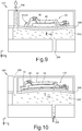
- FIGS 9 and 10 show schematically, in a cross-sectional view, a fluid ejection device 200 in respective operating states.
- the fluid ejection device 200 includes a body 201, e.g. of semiconductor material, within which a chamber 202 is present, adapted to be filled with a fluid that is to be ejected.
- the fluid is charged through an inlet channel 204 and ejected through a nozzle 206, both formed in the body 201 and fluidically coupled to the chamber 204.
- a membrane layer 208 faces the chamber 202.
- the piezoelectric transducer 100 is mechanically coupled to the membrane layer 208 and is isolated from the fluid in the chamber 202.
- the piezoelectric transducer 100 can be arranged on the membrane layer on a side of the membrane layer 208 that directly faces the chamber 202 and which is immersed, during use, in the fluid.
- the piezoelectric element 36 is controlled through the top electrode 48 and the bottom electrode 40 (which are biased through electrical connections, not shown) in such a way as to generate a deflection of the membrane layer 208 towards the inside of the chamber 202 (arrow D1). Said deflection causes a movement of the fluid through towards the nozzle 206 and generates a controlled expulsion of a drop towards the outside of the fluid ejection device 200.
- the piezoelectric element 36 is controlled through the top electrode 48 and the bottom electrode 40 (which are biased through the electrical connections) in such a way as to generate a deflection of the membrane layer 208 in a direction opposite to that of Figure 9 (arrow D2) so as to increase the volume of the chamber 202 and thus recalling further fluid towards the chamber 202 through the inlet channel 204.
- the chamber 202 is hence recharged with fluid.
- the piezoelectric element may then again be actuated for the expulsion of a further drop of fluid.
- the steps of Figures 9 and 10 are repeated throughout the fluid-ejecting process.
- Actuation of the piezoelectric element by biasing the top electrode 48 and bottom electrode 40 is in itself known and not described in further detail.
- piezoelectric transducer 100 can be employed in a variety of technical fields and applications, not limited to the fluid-ejection technology.
- the top electrode 48 is not exposed to PZT resist/mask removal and cleaning steps, and therefore it is not subjected to possible damages deriving from said steps.
- the top electrode 48 is formed only after etching / patterning steps of the bottom electrode 40, the top electrode 48 is not exposed to resist/mask removal and cleaning steps performed in connection with the manufacturing of the bottom electrode 40, which may damage the top electrode 48.
- the passivation layer 42 is formed before top electrode 48 formation, the top electrode 48, and the piezoelectric stack itself, are not subjected to thermal budgets related to the manufacturing of the passivation layer 42, which may damage the top electrode 48.
- the top electrode 48 is not subjected to vias etch and cleaning steps, which may damage the top electrode 48.
- steps of (i) forming the top electrode 48 and (ii) the conductive stripes 51, 52 are, in an embodiment, carried out at the same time. Therefore, further thermal budgets associated to a separate formation of the conductive stripes 51, 52 are avoided.
- intermediate layers may be formed between the bottom electrode 34 and the piezoelectric element 36, and/or between the top electrode 48 and the piezoelectric element 36, with the aim of enhancing the electrical contact between them and/or the reciprocal mechanical adhesion.
Landscapes
- Engineering & Computer Science (AREA)
- Manufacturing & Machinery (AREA)
- Chemical & Material Sciences (AREA)
- Ceramic Engineering (AREA)
- Particle Formation And Scattering Control In Inkjet Printers (AREA)
- Piezo-Electric Transducers For Audible Bands (AREA)
- Transducers For Ultrasonic Waves (AREA)
Abstract
Description
- The present invention relates to a method of manufacturing a piezoelectric transducer, and to a piezoelectric transducer.
- It is known to manufacture piezoelectric-based transducers, or actuators, such as for example PZT (Pb, Zr, TiO3) material. The piezoelectric transducers may then be used in a variety of technical fields, such as for inkjet, autofocus, speakers, etc.
- Usually, the piezoelectric transducer includes a stack where a piezoelectric element is sandwiched between a bottom electrode and a top electrode. Proper biasing of the top and bottom electrodes actuates the PZT element according to the needs.
- The top electrode is usually sputtered directly on top of the piezoelectric element and both layers are then etched (e.g., with a same photoresist mask). The bottom electrode is instead patterned with a dedicated etching step. The whole stack is then passivated, vias are formed through the passivation layer to form the electrical contacts for bias and metal stripes/pads are formed through a further metal deposition and etch.
- The top electrode, in the standard process flow, is therefore subjected to several process steps, which may affect its integrity and reliability. At the same time, also the piezoelectric element undergoes process steps which may alter its properties and the piezoelectric physical response as a function of the biasing voltage, leading to premature piezoelectric aging.
-
Figures 1A-1D illustrates, in lateral cross-sectional view, a process flow for manufacturing a stacked piezoelectric transducer, or actuator, according to an embodiment which is not part of the present invention. - With reference to
Figure 1A , a wafer 1 is provided, including asubstrate 2 made of semiconductor material, such as silicon. On afirst surface 2a of thesubstrate 2 a stack including a piezoelectric element and electrodes for actuation of the piezoelectric element is formed. The formation of the stack includes depositing a first layer ofconductive material 4; then, on the first layer ofconductive material 4, a layer of piezoelectric material 6-, is deposited; then, on the layer ofpiezoelectric material 6 is deposited a second layer ofconductive material 8, for example a metal material such as for example Ru or Pt. - Then,
Figure 1B , amask 11 is formed or arranged on the second layer ofconductive material 8, to cover an area of the second layer ofconductive material 8 corresponding to portions of the latter that will form, subsequently, a top electrode for actuating thepiezoelectric element 6. An etching step (e.g., dry etching) allows to remove portions of the second layer ofconductive material 8 not protected by themask 11. Using thesame mask 11, but a different etching chemistry, etching of the wafer 1 (e.g., dry etching) is continued to remove exposed portions of the layer ofpiezoelectric material 6 so as to form a piezoelectric element. Etching is stopped at the first layer ofconductive material 4, and themask 11 is removed. - One or more after-etch cleaning step may then be carried out.
- Then,
Figure 1C , a mask 15 (for example, a photoresist mask) is formed; themask 15 is designed to protect thetop electrode 8 and thepiezoelectric element 6, and to expose portions of the first layer ofconductive material 4 which has to be removed. An etching step is then carried out, to remove the portions of the first layer ofconductive material 4 not protected by themask 15. A bottom electrode, for actuating thepiezoelectric element 6 during use, is thus formed. - Then, the
mask 15 is removed from the wafer 1, and a step of deposition of apassivation layer 18 on the wafer 1 is carried out. Thepassivation layer 18 is, for example, silicon oxide (SiO2) deposited by CVD. - With reference to
Figure 1D , vias 17 are opened through thepassivation layer 18, using thetop electrode 6 and thebottom electrode 4 as stopping layers, to expose surface regions of the top and of thebottom electrodes conductive stripes - The
conductive stripes top electrode 8 and thebottom electrode 4 so as to activate thepiezoelectric element 6. - As it is apparent from the above, the
top electrode 8 is exposed to several process steps, including chemicals usually used to clean the stack after the dry etch, all these steps affecting negatively the top electrode performances and integrity. Also the cleaning steps of thebottom electrode 4 may have an impact on thetop electrode 8, e.g. by changing its conductivity properties (sheet resistance and morphology). To avoid, or limit in part, the negative impacts on the top electrodes, specific materials may be selected for the top electrode, thus limiting the process integration capabilities. - It is also noted that the
top electrode 8 is the stopping layer for the vias etch, which may significantly impact on its integrity. - Furthermore, the
piezoelectric element 6 withtop electrode 8 is subjected to several thermal budgets during manufacturing, e.g. during the passivation deposition and metal deposition, which is undesired. In fact, it is well known that piezoelectric properties of the above-described stacked structure are affected by annealing treatments. - The aim of the present invention is to provide a method of manufacturing a piezoelectric transducer, and a piezoelectric transducer, that overcome the drawbacks of the known art.
- According to the present invention, a method of manufacturing a piezoelectric transducer, and a piezoelectric transducer, are provided, as defined in the annexed claims.
- For a better understanding of the present invention, preferred embodiments thereof are now described purely by way of non-limiting example with reference to the attached drawings, wherein:
-
Figures 1A-1D show, in cross-sectional view, steps for manufacturing a piezoelectric transducer according to an embodiment which is not part of the present invention; -
Figures 2-8 show, in cross-sectional view, steps for manufacturing a piezoelectric transducer according to an embodiment of the present invention; and -
Figures 9 and 10 show a fluid-ejection device including the piezoelectric transducer manufactured according tofigures 2-8 during respective operative conditions. -
Figures 2-8 show, in a Cartesian (triaxial) reference system of axis X, Y, Z, steps for manufacturing a piezoelectric transducer, or actuator, according to an embodiment of the present invention. - With reference to
Figure 2 , awafer 30 is provided, including a semiconductor body 32 (in the following, named "substrate" without losing generality) made at least in part of semiconductor material, such as silicon or a silicon compound. - A
first electrode layer 34 is formed on afirst surface 32a of thesubstrate 32, in particular by depositing a conductive material such as metal, more in particular materials which can guarantee good piezoelectric layer orientation such as Platinum (Pt), Titanium/Platinum (TiPt) or Iridium (Ir). Then, on thefirst electrode layer 34, a piezoelectric layer, in particular doped or undoped PZT (Pb, Zr, TiO3) or a kind of lead-free perovskites material, is deposited and subsequently shaped, e.g. through photolithography, to form apiezoelectric element 36. This step may include the use of a mask (not shown) that and of an etching step (e.g., dry etching) to remove desired portions of the layer of piezoelectric layer so as to form thepiezoelectric element 36 having a designed shape. Etching is stopped at thefirst electrode layer 32, which is not removed. Thepiezoelectric element 36 has atop surface 36a opposite, along Z direction, to abottom surface 36b which directly faces (in particular, is in direct electrical contact with) thefirst electrode layer 34. - Then,
Figure 3 , a mask (for example, a photoresist mask, not shown) is formed; the mask is designed to protect thepiezoelectric element 36, and to let portions of thefirst electrode layer 34 that are to be removed exposed to an etchant. An etching step is then carried out, to remove the portions of thefirst electrode 34 not protected by the mask. Abottom electrode 40, for actuating thepiezoelectric element 6 during use, is thus formed. - Then, the mask is removed and a step of deposition of a
passivation layer 42 on thewafer 30 is carried out. Thepassivation layer 42 includes dielectric materials used for electrical insulation of the electrodes, for example SiO2 or SiN or Al2O layers, either as single layers or a plurality of layers stacked on one another. - With reference to
Figure 4 ,vias passivation layer 42, using thepiezoelectric element 36 and thebottom electrode 34 as stopping layers, to expose surface regions of thepiezoelectric element 36 and of thebottom electrode 34. In particular, it is noted that via 44 formed at thepiezoelectric element 36 has, in top-plan view, an extension (area) which is about the same as the extension (area) of thepiezoelectric element 36. The extension, in top-plan view, of thevia 44 is chosen such as to expose a surface portion of thepiezoelectric element 36 wide enough to provide sufficient contact area for a top electrode that will form, together with thebottom electrode 40, a piezoelectric stack for actuating thepiezoelectric element 36. For example, the exposed surface portion of thepiezoelectric element 36 is in the range 70-99% (ideally, 100%) of the surface area of thepiezoelectric element 36. The surface of thepiezoelectric element 36 considered in this context is thetop surface 36a of thepiezoelectric element 36 parallel to the XY plane and opposite, along the Z direction, to thebottom surface 36b of thepiezoelectric element 36 which is in direct contact with thebottom electrode 40. - Then,
Figure 5 , a step of formingtop electrode 48 is carried out, namely by depositing (e.g., sputtering) and patterning a film of conductive material, such as metal (e.g., Ru, TiW, Pt, Al, AlCu, Au, Mo, W-based materials) or not metallic conductive materials (e.g. C-based materials, metallic oxides, etc.). Thetop electrode 48 is formed within thevia 44, in particular in direct electrical contact with thepiezoelectric element 36. - According to an aspect of the present embodiment, concurrently to the step of forming the
top electrode 48, an optional step of formingconductive stripes bottom electrode 40 and thetop electrode 48, respectively. In particular, theconductive stripe 51 extends on thepassivation layer 42 in electrical and mechanical continuity with thetop electrode 48; theconductive stripe 52 extends within thevia 45, in electrical contact with thebottom electrode 40, and on thepassivation layer 42. As detailed in the following, theconductive stripes - According to another embodiment of the present invention, the electrical contacts can be formed directly at
layer 44 andlayer 45, as a function of the design and/or specific application requirements. That means that theconductive stripes - Then,
Figure 6 , apassivation layer 56 is formed on thewafer 30. The passivation layer 56can be either organic or inorganic, for example, silicon nitride (SixNy, in particular Si3N4) deposited by CVD. Thepassivation layer 56 completely covers thetop electrode 48, thebottom electrode 40 and theconductive stripes - Then,
Figure 7 ,openings passivation layer 56 to reach and expose selective portions of theconductive stripe 51 and, respectively, conductive stripe52. -
Metal contacts Figure 8 , within theopenings conductive stripes layers -
Metal contacts top electrode 48 and thebottom electrode 40 through theconductive stripes 51 and respectively52, so as to activate/operate thepiezoelectric element 36. - In an embodiment of the present invention, where the
conductive stripes metal contacts - A
piezoelectric transducer 100 is thus formed. - The
piezoelectric transducer 100 can be used, for example, to operate a liquid-ejection device. -
Figures 9 and 10 show schematically, in a cross-sectional view, afluid ejection device 200 in respective operating states. Thefluid ejection device 200 includes a body 201, e.g. of semiconductor material, within which achamber 202 is present, adapted to be filled with a fluid that is to be ejected. The fluid is charged through aninlet channel 204 and ejected through anozzle 206, both formed in the body 201 and fluidically coupled to thechamber 204. Amembrane layer 208 faces thechamber 202. - In this case, the
piezoelectric transducer 100 is mechanically coupled to themembrane layer 208 and is isolated from the fluid in thechamber 202. According to an alternative embodiment, not shown, thepiezoelectric transducer 100 can be arranged on the membrane layer on a side of themembrane layer 208 that directly faces thechamber 202 and which is immersed, during use, in the fluid. - With reference to
Figure 9 , thepiezoelectric element 36 is controlled through thetop electrode 48 and the bottom electrode 40 (which are biased through electrical connections, not shown) in such a way as to generate a deflection of themembrane layer 208 towards the inside of the chamber 202 (arrow D1). Said deflection causes a movement of the fluid through towards thenozzle 206 and generates a controlled expulsion of a drop towards the outside of thefluid ejection device 200. - With reference to
Figure 10 , thepiezoelectric element 36 is controlled through thetop electrode 48 and the bottom electrode 40 (which are biased through the electrical connections) in such a way as to generate a deflection of themembrane layer 208 in a direction opposite to that ofFigure 9 (arrow D2) so as to increase the volume of thechamber 202 and thus recalling further fluid towards thechamber 202 through theinlet channel 204. Thechamber 202 is hence recharged with fluid. - The piezoelectric element may then again be actuated for the expulsion of a further drop of fluid. The steps of
Figures 9 and 10 are repeated throughout the fluid-ejecting process. - Actuation of the piezoelectric element by biasing the
top electrode 48 andbottom electrode 40 is in itself known and not described in further detail. - It is apparent that the
piezoelectric transducer 100 can be employed in a variety of technical fields and applications, not limited to the fluid-ejection technology. - From an examination of the characteristics of the invention provided according to the present disclosure, the advantages that it affords are evident.
- In particular, since the
PZT element 36 is patterned before thetop electrode 48 deposition, thetop electrode 48 is not exposed to PZT resist/mask removal and cleaning steps, and therefore it is not subjected to possible damages deriving from said steps. - Moreover, since the
top electrode 48 is formed only after etching / patterning steps of thebottom electrode 40, thetop electrode 48 is not exposed to resist/mask removal and cleaning steps performed in connection with the manufacturing of thebottom electrode 40, which may damage thetop electrode 48. - Moreover, since the
passivation layer 42 is formed beforetop electrode 48 formation, thetop electrode 48, and the piezoelectric stack itself, are not subjected to thermal budgets related to the manufacturing of thepassivation layer 42, which may damage thetop electrode 48. - Moreover, since the vias/
apertures passivation layer 42 are formed before thetop electrode 48 formation, thetop electrode 48 is not subjected to vias etch and cleaning steps, which may damage thetop electrode 48. - Moreover, the steps of (i) forming the
top electrode 48 and (ii) theconductive stripes conductive stripes - Finally, it is clear that modifications and variations may be made to what has been described and illustrated herein, without thereby departing from the sphere of protection of the present invention, as defined in the annexed claims.
- For example, intermediate layers (not shown in the drawings) may be formed between the
bottom electrode 34 and thepiezoelectric element 36, and/or between thetop electrode 48 and thepiezoelectric element 36, with the aim of enhancing the electrical contact between them and/or the reciprocal mechanical adhesion.
Claims (12)
- A method for manufacturing a piezoelectric transducer (100), comprising the steps of:- forming, on a semiconductor body (32), a bottom electrode (34) of conductive material;- forming, on the bottom electrode (34), a piezoelectric element (36); and- forming, on the bottom electrode (34) and the piezoelectric element (36), a first protective layer (42) having a first opening (44) through which a portion of said piezoelectric element (36) is exposed, and a second opening (45) through which a portion of said bottom electrode (34) is exposed,characterized by further comprising the steps of:- forming, on the first protective layer (42) and within the first and second openings (44, 45), a conductive layer (48, 51, 52); and- patterning said conductive layer (48, 51, 52) to contextually form:a top electrode (48) in electrical contact with the piezoelectric element (36) at said first opening (44),a first biasing stripe (51) in electrical contact with the top electrode (48), anda second biasing stripe (52) in electrical contact with the bottom electrode (40) at said second opening (45).
- The method according to claim 1, further comprising the steps of:- forming a second protective layer (56) on the top electrode (48), first biasing stripe (51) and second biasing stripe (52); and- etching the second protective layer (56) at said first biasing stripe (51) and second biasing stripe (52) to form first and second vias (58, 59) for electrically contacting the first biasing stripe (51) and, respectively, the second biasing stripe (52).
- The method of claim 1 or 2, wherein the step of forming the first protective layer (42) includes:- depositing a plurality of passivation layers completely covering the piezoelectric element (36) and the bottom electrode (40);- locally removing said plurality of passivation layers at said piezoelectric element (36), thus forming the first opening (44); and- locally removing said plurality of passivation layers at said bottom electrode (40), laterally staggered with respect to said piezoelectric element (36), thus forming the second opening (45).
- The method according to claim 3, wherein said plurality of passivation layers include an Aluminum Oxide layer and a Silicon Dioxide, layer.
- The method according to anyone of the preceding claims, wherein the step of forming the conductive layer (48, 51, 52) includes sputtering metal material on the first protective layer (42) and within the first and second openings (44, 45);
and wherein the step of patterning the conductive layer (48, 51, 52) includes etching selective portions of the sputtered metal material on the first protective layer (42) to electrically isolate said sputtered metal material in the first opening (44) from the sputtered metal material in the second opening (45). - The method according to claim 5, wherein etching selective portions of the sputtered metal material on the first protective layer (42) includes carry out an etching step using an etching mask which is shaped in such a way to allow removal of the sputtered metal material with the exception of regions of the sputtered metal material which are designed to form said top electrode (48), first biasing stripe (51) and second biasing stripe (52).
- The method according to anyone of the preceding claims, wherein said piezoelectric element (36) is of PZT material.
- A piezoelectric transducer (100), comprising:- a bottom electrode (34), of conductive material, on a semiconductor body (32);- a piezoelectric element (36) on, and in direct electrical contact with, the bottom electrode (34);- a first protective layer (42), extending on the bottom electrode (34) and on the piezoelectric element (36), having a first opening (44) reaching a portion of said piezoelectric element (36), and a second opening (45) reaching a portion of said bottom electrode (34);- a top electrode (48) in direct electrical contact with the piezoelectric element (36) through said first opening (44);- a first biasing stripe (51) on the first protective layer (42), in direct electrical contact with the top electrode (48); and- a second biasing stripe (52) on the first protective layer (42), in direct electrical contact with the bottom electrode (40) through said second opening (45).
- The piezoelectric transducer (100) according to claim 8, further comprising a second protective layer (56) extending on, and in direct contact with, the top electrode (48), the first biasing stripe (51) and the second biasing stripe (52).,
wherein the second protective layer (56) has a first via (58) at said first biasing stripe (51), and second via (59) at said second biasing stripe (52), exposing a surface portion of the first biasing stripe (51) and, respectively, of the second biasing stripe (52). - The piezoelectric transducer (100) according to claim 8 or 9, wherein the first protective layer (42) includes a plurality of stacked passivation layers, in particular an Aluminum Oxide layer and a Silicon Dioxide layer.
- The piezoelectric transducer (100) according to anyone of claims 8-10, wherein said piezoelectric element (36) is of PZT material.
- A fluid ejection device (200), including:- a body (201), having an inlet hole and an outlet nozzle;- an chamber (202) within said body (201), configured to house a fluid to be ejected, fluidically coupled between said inlet hole and an outlet nozzle;- a membrane (208) facing the inner chamber (202);- a piezoelectric actuator (100) according to anyone of claims 8-10, arranged on the membrane (208) and configured to be actuated in such a way to cause a displacement of the membrane (208) towards the first chamber and/or, alternatively, away from the first chamber.
Applications Claiming Priority (1)
| Application Number | Priority Date | Filing Date | Title |
|---|---|---|---|
| IT102019000007213A IT201900007213A1 (en) | 2019-05-24 | 2019-05-24 | METHOD OF MANUFACTURING A STACKED PIEZOELECTRIC TRANSDUCER AND PIEZOELECTRIC TRANSDUCER |
Publications (2)
| Publication Number | Publication Date |
|---|---|
| EP3742506A1 true EP3742506A1 (en) | 2020-11-25 |
| EP3742506B1 EP3742506B1 (en) | 2023-09-06 |
Family
ID=67876038
Family Applications (1)
| Application Number | Title | Priority Date | Filing Date |
|---|---|---|---|
| EP20176147.5A Active EP3742506B1 (en) | 2019-05-24 | 2020-05-22 | Piezoelectric transducer and method of manufacturing thereof |
Country Status (4)
| Country | Link |
|---|---|
| US (1) | US11433669B2 (en) |
| EP (1) | EP3742506B1 (en) |
| CN (2) | CN111987213A (en) |
| IT (1) | IT201900007213A1 (en) |
Cited By (2)
| Publication number | Priority date | Publication date | Assignee | Title |
|---|---|---|---|---|
| WO2022172672A1 (en) * | 2021-02-12 | 2022-08-18 | 住友化学株式会社 | Piezoelectric laminate, piezoelectric element, and method for manufacturing piezoelectric laminate |
| TWI917532B (en) | 2021-02-12 | 2026-03-11 | 日商住友化學股份有限公司 | Piezoelectric stack, piezoelectric element, and method of manufacturing piezoelectric stack |
Families Citing this family (3)
| Publication number | Priority date | Publication date | Assignee | Title |
|---|---|---|---|---|
| IT201900007213A1 (en) * | 2019-05-24 | 2020-11-24 | St Microelectronics Srl | METHOD OF MANUFACTURING A STACKED PIEZOELECTRIC TRANSDUCER AND PIEZOELECTRIC TRANSDUCER |
| IT202000010264A1 (en) * | 2020-05-07 | 2021-11-07 | St Microelectronics Srl | PIEZOELECTRIC ACTUATOR HAVING A DEFORMATION SENSOR AND RELATED MANUFACTURING PROCEDURE |
| IT202000010261A1 (en) | 2020-05-07 | 2021-11-07 | St Microelectronics Srl | PIEZOELECTRIC ACTUATOR EQUIPPED WITH A DEFORMABLE STRUCTURE HAVING IMPROVED MECHANICAL PROPERTIES AND RELATED MANUFACTURING PROCEDURE |
Citations (3)
| Publication number | Priority date | Publication date | Assignee | Title |
|---|---|---|---|---|
| US5481490A (en) * | 1993-10-12 | 1996-01-02 | Olympus Optical Co., Ltd. | Ferroelectric memory |
| EP3173235A1 (en) * | 2015-11-30 | 2017-05-31 | STMicroelectronics Srl | Fluid ejection device with restriction channel, and manufacturing method thereof |
| US20180079210A1 (en) * | 2016-09-20 | 2018-03-22 | Rohm Co., Ltd. | Ink jet print head and method of manufacturing the same |
Family Cites Families (9)
| Publication number | Priority date | Publication date | Assignee | Title |
|---|---|---|---|---|
| KR101856060B1 (en) * | 2011-12-01 | 2018-05-10 | 삼성전자주식회사 | Bulk acoustic wave resonator |
| JP6399386B2 (en) * | 2014-07-02 | 2018-10-03 | 株式会社リコー | Electromechanical conversion member manufacturing method, droplet discharge head manufacturing method, and image forming apparatus manufacturing method |
| JP2016060164A (en) * | 2014-09-19 | 2016-04-25 | セイコーエプソン株式会社 | Piezoelectric element, liquid ejecting head, liquid ejecting apparatus, and method of manufacturing piezoelectric element |
| US9776405B2 (en) * | 2014-10-08 | 2017-10-03 | Rohm Co., Ltd. | Inkjet apparatus and manufacturing method of inkjet apparatus |
| JP2017085005A (en) * | 2015-10-29 | 2017-05-18 | 株式会社リコー | Piezoelectric actuator and method for manufacturing piezoelectric actuator |
| ITUB20159729A1 (en) * | 2015-12-29 | 2017-06-29 | St Microelectronics Srl | METHOD OF MANUFACTURING A IMPROVED FLUID EJECTION DEVICE, AND FLUID EJECTION DEVICE |
| JP6829558B2 (en) * | 2016-08-04 | 2021-02-10 | ローム株式会社 | Piezoelectric element utilization device and its manufacturing method |
| IT201800001152A1 (en) * | 2018-01-17 | 2019-07-17 | St Microelectronics Srl | MANUFACTURING METHOD OF A FLUID EJECTION DEVICE WITH IMPROVED RESONANCE FREQUENCY AND FLUID EJECTION SPEED, AND FLUID EJECTION DEVICE |
| IT201900007213A1 (en) * | 2019-05-24 | 2020-11-24 | St Microelectronics Srl | METHOD OF MANUFACTURING A STACKED PIEZOELECTRIC TRANSDUCER AND PIEZOELECTRIC TRANSDUCER |
-
2019
- 2019-05-24 IT IT102019000007213A patent/IT201900007213A1/en unknown
-
2020
- 2020-05-20 US US16/879,269 patent/US11433669B2/en active Active
- 2020-05-22 EP EP20176147.5A patent/EP3742506B1/en active Active
- 2020-05-22 CN CN202010444097.0A patent/CN111987213A/en active Pending
- 2020-05-22 CN CN202020878400.3U patent/CN212182361U/en active Active
Patent Citations (3)
| Publication number | Priority date | Publication date | Assignee | Title |
|---|---|---|---|---|
| US5481490A (en) * | 1993-10-12 | 1996-01-02 | Olympus Optical Co., Ltd. | Ferroelectric memory |
| EP3173235A1 (en) * | 2015-11-30 | 2017-05-31 | STMicroelectronics Srl | Fluid ejection device with restriction channel, and manufacturing method thereof |
| US20180079210A1 (en) * | 2016-09-20 | 2018-03-22 | Rohm Co., Ltd. | Ink jet print head and method of manufacturing the same |
Non-Patent Citations (1)
| Title |
|---|
| DUBOIS M-A ET AL: "PZT Thin Film Actuated Elastic Fin Micromotor", IEEE TRANSACTIONS ON ULTRASONICS, FERROELECTRICS, AND FREQUENCY CONTROL, vol. 45, no. 5, September 1998 (1998-09-01), pages 1169 - 1177, XP011437806, ISSN: 0885-3010, DOI: 10.1109/58.726440 * |
Cited By (3)
| Publication number | Priority date | Publication date | Assignee | Title |
|---|---|---|---|---|
| WO2022172672A1 (en) * | 2021-02-12 | 2022-08-18 | 住友化学株式会社 | Piezoelectric laminate, piezoelectric element, and method for manufacturing piezoelectric laminate |
| JPWO2022172672A1 (en) * | 2021-02-12 | 2022-08-18 | ||
| TWI917532B (en) | 2021-02-12 | 2026-03-11 | 日商住友化學股份有限公司 | Piezoelectric stack, piezoelectric element, and method of manufacturing piezoelectric stack |
Also Published As
| Publication number | Publication date |
|---|---|
| US11433669B2 (en) | 2022-09-06 |
| US20200369029A1 (en) | 2020-11-26 |
| CN111987213A (en) | 2020-11-24 |
| CN212182361U (en) | 2020-12-18 |
| IT201900007213A1 (en) | 2020-11-24 |
| EP3742506B1 (en) | 2023-09-06 |
Similar Documents
| Publication | Publication Date | Title |
|---|---|---|
| EP3742506B1 (en) | Piezoelectric transducer and method of manufacturing thereof | |
| US11084283B2 (en) | Methods of forming and using fluid ejection devices and printheads | |
| CN111762753B (en) | Micro-electromechanical system device and forming method thereof | |
| US9065358B2 (en) | MEMS structure and method of forming same | |
| JP5204171B2 (en) | Electrical component and manufacturing method thereof | |
| US10946653B2 (en) | Fluid ejection microfluidic device, in particular for ink printing, and manufacturing process thereof | |
| JP4492821B2 (en) | Piezoelectric element | |
| US20180065371A1 (en) | Manufacturing method for a fluid-ejection device, and fluid-ejection device | |
| EP3173235A1 (en) | Fluid ejection device with restriction channel, and manufacturing method thereof | |
| US11498335B2 (en) | Method for manufacturing a fluid-ejection device with improved resonance frequency and fluid ejection velocity, and fluid-ejection device | |
| JP2018089892A (en) | Liquid discharge head | |
| US7851976B2 (en) | Micro movable device and method of making the same using wet etching | |
| JP2013080786A (en) | Silicon device | |
| JP6427157B2 (en) | Ink nozzle and ink jet printer head having the same | |
| US9181081B2 (en) | Electrical component and method of manufacturing the same | |
| CN112802958B (en) | Piezoelectric device and method of forming the same | |
| CN212499504U (en) | Fluid ejection apparatus and system for fluid ejection | |
| JP2010251590A (en) | Semiconductor device and manufacturing method thereof | |
| US7723822B2 (en) | MEMS element having a dummy pattern | |
| CN113307222B (en) | Micro-electromechanical system and method for manufacturing the same | |
| US20250214341A1 (en) | Manufacturing method of liquid ejection head and liquid ejection head | |
| US10265956B2 (en) | Liquid ejection head and method of manufacturing liquid ejection head | |
| US20250072291A1 (en) | Piezoelectric element, method for manufacturing piezoelectric element, and liquid ejection head | |
| US20260138865A1 (en) | Bumpstop process for a motion sensor |
Legal Events
| Date | Code | Title | Description |
|---|---|---|---|
| PUAI | Public reference made under article 153(3) epc to a published international application that has entered the european phase |
Free format text: ORIGINAL CODE: 0009012 |
|
| STAA | Information on the status of an ep patent application or granted ep patent |
Free format text: STATUS: THE APPLICATION HAS BEEN PUBLISHED |
|
| AK | Designated contracting states |
Kind code of ref document: A1 Designated state(s): AL AT BE BG CH CY CZ DE DK EE ES FI FR GB GR HR HU IE IS IT LI LT LU LV MC MK MT NL NO PL PT RO RS SE SI SK SM TR |
|
| AX | Request for extension of the european patent |
Extension state: BA ME |
|
| STAA | Information on the status of an ep patent application or granted ep patent |
Free format text: STATUS: REQUEST FOR EXAMINATION WAS MADE |
|
| 17P | Request for examination filed |
Effective date: 20210330 |
|
| RBV | Designated contracting states (corrected) |
Designated state(s): AL AT BE BG CH CY CZ DE DK EE ES FI FR GB GR HR HU IE IS IT LI LT LU LV MC MK MT NL NO PL PT RO RS SE SI SK SM TR |
|
| STAA | Information on the status of an ep patent application or granted ep patent |
Free format text: STATUS: EXAMINATION IS IN PROGRESS |
|
| 17Q | First examination report despatched |
Effective date: 20211006 |
|
| REG | Reference to a national code |
Ref country code: DE Ref legal event code: R079 Free format text: PREVIOUS MAIN CLASS: H01L0041290000 Ref country code: DE Ref legal event code: R079 Ref document number: 602020017045 Country of ref document: DE Free format text: PREVIOUS MAIN CLASS: H01L0041290000 Ipc: H10N0030020000 |
|
| GRAP | Despatch of communication of intention to grant a patent |
Free format text: ORIGINAL CODE: EPIDOSNIGR1 |
|
| STAA | Information on the status of an ep patent application or granted ep patent |
Free format text: STATUS: GRANT OF PATENT IS INTENDED |
|
| RIC1 | Information provided on ipc code assigned before grant |
Ipc: B41J 2/14 20060101ALI20230224BHEP Ipc: H10N 30/88 20230101ALI20230224BHEP Ipc: H10N 30/87 20230101ALI20230224BHEP Ipc: H10N 30/20 20230101ALI20230224BHEP Ipc: H10N 30/06 20230101ALI20230224BHEP Ipc: H10N 30/02 20230101AFI20230224BHEP |
|
| INTG | Intention to grant announced |
Effective date: 20230331 |
|
| GRAS | Grant fee paid |
Free format text: ORIGINAL CODE: EPIDOSNIGR3 |
|
| GRAA | (expected) grant |
Free format text: ORIGINAL CODE: 0009210 |
|
| STAA | Information on the status of an ep patent application or granted ep patent |
Free format text: STATUS: THE PATENT HAS BEEN GRANTED |
|
| AK | Designated contracting states |
Kind code of ref document: B1 Designated state(s): AL AT BE BG CH CY CZ DE DK EE ES FI FR GB GR HR HU IE IS IT LI LT LU LV MC MK MT NL NO PL PT RO RS SE SI SK SM TR |
|
| REG | Reference to a national code |
Ref country code: GB Ref legal event code: FG4D |
|
| REG | Reference to a national code |
Ref country code: CH Ref legal event code: EP |
|
| REG | Reference to a national code |
Ref country code: DE Ref legal event code: R096 Ref document number: 602020017045 Country of ref document: DE |
|
| REG | Reference to a national code |
Ref country code: IE Ref legal event code: FG4D |
|
| REG | Reference to a national code |
Ref country code: LT Ref legal event code: MG9D |
|
| REG | Reference to a national code |
Ref country code: NL Ref legal event code: MP Effective date: 20230906 |
|
| PG25 | Lapsed in a contracting state [announced via postgrant information from national office to epo] |
Ref country code: GR Free format text: LAPSE BECAUSE OF FAILURE TO SUBMIT A TRANSLATION OF THE DESCRIPTION OR TO PAY THE FEE WITHIN THE PRESCRIBED TIME-LIMIT Effective date: 20231207 |
|
| PG25 | Lapsed in a contracting state [announced via postgrant information from national office to epo] |
Ref country code: SE Free format text: LAPSE BECAUSE OF FAILURE TO SUBMIT A TRANSLATION OF THE DESCRIPTION OR TO PAY THE FEE WITHIN THE PRESCRIBED TIME-LIMIT Effective date: 20230906 Ref country code: RS Free format text: LAPSE BECAUSE OF FAILURE TO SUBMIT A TRANSLATION OF THE DESCRIPTION OR TO PAY THE FEE WITHIN THE PRESCRIBED TIME-LIMIT Effective date: 20230906 Ref country code: NO Free format text: LAPSE BECAUSE OF FAILURE TO SUBMIT A TRANSLATION OF THE DESCRIPTION OR TO PAY THE FEE WITHIN THE PRESCRIBED TIME-LIMIT Effective date: 20231206 Ref country code: LV Free format text: LAPSE BECAUSE OF FAILURE TO SUBMIT A TRANSLATION OF THE DESCRIPTION OR TO PAY THE FEE WITHIN THE PRESCRIBED TIME-LIMIT Effective date: 20230906 Ref country code: LT Free format text: LAPSE BECAUSE OF FAILURE TO SUBMIT A TRANSLATION OF THE DESCRIPTION OR TO PAY THE FEE WITHIN THE PRESCRIBED TIME-LIMIT Effective date: 20230906 Ref country code: HR Free format text: LAPSE BECAUSE OF FAILURE TO SUBMIT A TRANSLATION OF THE DESCRIPTION OR TO PAY THE FEE WITHIN THE PRESCRIBED TIME-LIMIT Effective date: 20230906 Ref country code: GR Free format text: LAPSE BECAUSE OF FAILURE TO SUBMIT A TRANSLATION OF THE DESCRIPTION OR TO PAY THE FEE WITHIN THE PRESCRIBED TIME-LIMIT Effective date: 20231207 Ref country code: FI Free format text: LAPSE BECAUSE OF FAILURE TO SUBMIT A TRANSLATION OF THE DESCRIPTION OR TO PAY THE FEE WITHIN THE PRESCRIBED TIME-LIMIT Effective date: 20230906 |
|
| REG | Reference to a national code |
Ref country code: AT Ref legal event code: MK05 Ref document number: 1610309 Country of ref document: AT Kind code of ref document: T Effective date: 20230906 |
|
| PG25 | Lapsed in a contracting state [announced via postgrant information from national office to epo] |
Ref country code: NL Free format text: LAPSE BECAUSE OF FAILURE TO SUBMIT A TRANSLATION OF THE DESCRIPTION OR TO PAY THE FEE WITHIN THE PRESCRIBED TIME-LIMIT Effective date: 20230906 |
|
| PG25 | Lapsed in a contracting state [announced via postgrant information from national office to epo] |
Ref country code: IS Free format text: LAPSE BECAUSE OF FAILURE TO SUBMIT A TRANSLATION OF THE DESCRIPTION OR TO PAY THE FEE WITHIN THE PRESCRIBED TIME-LIMIT Effective date: 20240106 |
|
| PG25 | Lapsed in a contracting state [announced via postgrant information from national office to epo] |
Ref country code: AT Free format text: LAPSE BECAUSE OF FAILURE TO SUBMIT A TRANSLATION OF THE DESCRIPTION OR TO PAY THE FEE WITHIN THE PRESCRIBED TIME-LIMIT Effective date: 20230906 |
|
| PG25 | Lapsed in a contracting state [announced via postgrant information from national office to epo] |
Ref country code: ES Free format text: LAPSE BECAUSE OF FAILURE TO SUBMIT A TRANSLATION OF THE DESCRIPTION OR TO PAY THE FEE WITHIN THE PRESCRIBED TIME-LIMIT Effective date: 20230906 |
|
| PG25 | Lapsed in a contracting state [announced via postgrant information from national office to epo] |
Ref country code: SM Free format text: LAPSE BECAUSE OF FAILURE TO SUBMIT A TRANSLATION OF THE DESCRIPTION OR TO PAY THE FEE WITHIN THE PRESCRIBED TIME-LIMIT Effective date: 20230906 Ref country code: RO Free format text: LAPSE BECAUSE OF FAILURE TO SUBMIT A TRANSLATION OF THE DESCRIPTION OR TO PAY THE FEE WITHIN THE PRESCRIBED TIME-LIMIT Effective date: 20230906 Ref country code: IS Free format text: LAPSE BECAUSE OF FAILURE TO SUBMIT A TRANSLATION OF THE DESCRIPTION OR TO PAY THE FEE WITHIN THE PRESCRIBED TIME-LIMIT Effective date: 20240106 Ref country code: ES Free format text: LAPSE BECAUSE OF FAILURE TO SUBMIT A TRANSLATION OF THE DESCRIPTION OR TO PAY THE FEE WITHIN THE PRESCRIBED TIME-LIMIT Effective date: 20230906 Ref country code: EE Free format text: LAPSE BECAUSE OF FAILURE TO SUBMIT A TRANSLATION OF THE DESCRIPTION OR TO PAY THE FEE WITHIN THE PRESCRIBED TIME-LIMIT Effective date: 20230906 Ref country code: CZ Free format text: LAPSE BECAUSE OF FAILURE TO SUBMIT A TRANSLATION OF THE DESCRIPTION OR TO PAY THE FEE WITHIN THE PRESCRIBED TIME-LIMIT Effective date: 20230906 Ref country code: AT Free format text: LAPSE BECAUSE OF FAILURE TO SUBMIT A TRANSLATION OF THE DESCRIPTION OR TO PAY THE FEE WITHIN THE PRESCRIBED TIME-LIMIT Effective date: 20230906 Ref country code: SK Free format text: LAPSE BECAUSE OF FAILURE TO SUBMIT A TRANSLATION OF THE DESCRIPTION OR TO PAY THE FEE WITHIN THE PRESCRIBED TIME-LIMIT Effective date: 20230906 Ref country code: PT Free format text: LAPSE BECAUSE OF FAILURE TO SUBMIT A TRANSLATION OF THE DESCRIPTION OR TO PAY THE FEE WITHIN THE PRESCRIBED TIME-LIMIT Effective date: 20240108 |
|
| PG25 | Lapsed in a contracting state [announced via postgrant information from national office to epo] |
Ref country code: PL Free format text: LAPSE BECAUSE OF FAILURE TO SUBMIT A TRANSLATION OF THE DESCRIPTION OR TO PAY THE FEE WITHIN THE PRESCRIBED TIME-LIMIT Effective date: 20230906 Ref country code: IT Free format text: LAPSE BECAUSE OF FAILURE TO SUBMIT A TRANSLATION OF THE DESCRIPTION OR TO PAY THE FEE WITHIN THE PRESCRIBED TIME-LIMIT Effective date: 20230906 |
|
| REG | Reference to a national code |
Ref country code: DE Ref legal event code: R097 Ref document number: 602020017045 Country of ref document: DE |
|
| PG25 | Lapsed in a contracting state [announced via postgrant information from national office to epo] |
Ref country code: DK Free format text: LAPSE BECAUSE OF FAILURE TO SUBMIT A TRANSLATION OF THE DESCRIPTION OR TO PAY THE FEE WITHIN THE PRESCRIBED TIME-LIMIT Effective date: 20230906 |
|
| PLBE | No opposition filed within time limit |
Free format text: ORIGINAL CODE: 0009261 |
|
| STAA | Information on the status of an ep patent application or granted ep patent |
Free format text: STATUS: NO OPPOSITION FILED WITHIN TIME LIMIT |
|
| PG25 | Lapsed in a contracting state [announced via postgrant information from national office to epo] |
Ref country code: DK Free format text: LAPSE BECAUSE OF FAILURE TO SUBMIT A TRANSLATION OF THE DESCRIPTION OR TO PAY THE FEE WITHIN THE PRESCRIBED TIME-LIMIT Effective date: 20230906 Ref country code: SI Free format text: LAPSE BECAUSE OF FAILURE TO SUBMIT A TRANSLATION OF THE DESCRIPTION OR TO PAY THE FEE WITHIN THE PRESCRIBED TIME-LIMIT Effective date: 20230906 |
|
| 26N | No opposition filed |
Effective date: 20240607 |
|
| PG25 | Lapsed in a contracting state [announced via postgrant information from national office to epo] |
Ref country code: BG Free format text: LAPSE BECAUSE OF FAILURE TO SUBMIT A TRANSLATION OF THE DESCRIPTION OR TO PAY THE FEE WITHIN THE PRESCRIBED TIME-LIMIT Effective date: 20230906 |
|
| PG25 | Lapsed in a contracting state [announced via postgrant information from national office to epo] |
Ref country code: BG Free format text: LAPSE BECAUSE OF FAILURE TO SUBMIT A TRANSLATION OF THE DESCRIPTION OR TO PAY THE FEE WITHIN THE PRESCRIBED TIME-LIMIT Effective date: 20230906 |
|
| REG | Reference to a national code |
Ref country code: CH Ref legal event code: PL |
|
| PG25 | Lapsed in a contracting state [announced via postgrant information from national office to epo] |
Ref country code: MC Free format text: LAPSE BECAUSE OF FAILURE TO SUBMIT A TRANSLATION OF THE DESCRIPTION OR TO PAY THE FEE WITHIN THE PRESCRIBED TIME-LIMIT Effective date: 20230906 |
|
| PG25 | Lapsed in a contracting state [announced via postgrant information from national office to epo] |
Ref country code: LU Free format text: LAPSE BECAUSE OF NON-PAYMENT OF DUE FEES Effective date: 20240522 |
|
| GBPC | Gb: european patent ceased through non-payment of renewal fee |
Effective date: 20240522 |
|
| PG25 | Lapsed in a contracting state [announced via postgrant information from national office to epo] |
Ref country code: MC Free format text: LAPSE BECAUSE OF FAILURE TO SUBMIT A TRANSLATION OF THE DESCRIPTION OR TO PAY THE FEE WITHIN THE PRESCRIBED TIME-LIMIT Effective date: 20230906 Ref country code: LU Free format text: LAPSE BECAUSE OF NON-PAYMENT OF DUE FEES Effective date: 20240522 Ref country code: CH Free format text: LAPSE BECAUSE OF NON-PAYMENT OF DUE FEES Effective date: 20240531 |
|
| REG | Reference to a national code |
Ref country code: BE Ref legal event code: MM Effective date: 20240531 |
|
| PG25 | Lapsed in a contracting state [announced via postgrant information from national office to epo] |
Ref country code: IE Free format text: LAPSE BECAUSE OF NON-PAYMENT OF DUE FEES Effective date: 20240522 |
|
| PG25 | Lapsed in a contracting state [announced via postgrant information from national office to epo] |
Ref country code: BE Free format text: LAPSE BECAUSE OF NON-PAYMENT OF DUE FEES Effective date: 20240531 |
|
| PG25 | Lapsed in a contracting state [announced via postgrant information from national office to epo] |
Ref country code: FR Free format text: LAPSE BECAUSE OF NON-PAYMENT OF DUE FEES Effective date: 20240531 |
|
| PG25 | Lapsed in a contracting state [announced via postgrant information from national office to epo] |
Ref country code: GB Free format text: LAPSE BECAUSE OF NON-PAYMENT OF DUE FEES Effective date: 20240522 |
|
| PGFP | Annual fee paid to national office [announced via postgrant information from national office to epo] |
Ref country code: DE Payment date: 20250423 Year of fee payment: 6 |
|
| PG25 | Lapsed in a contracting state [announced via postgrant information from national office to epo] |
Ref country code: CY Free format text: LAPSE BECAUSE OF FAILURE TO SUBMIT A TRANSLATION OF THE DESCRIPTION OR TO PAY THE FEE WITHIN THE PRESCRIBED TIME-LIMIT; INVALID AB INITIO Effective date: 20200522 |
|
| PG25 | Lapsed in a contracting state [announced via postgrant information from national office to epo] |
Ref country code: HU Free format text: LAPSE BECAUSE OF FAILURE TO SUBMIT A TRANSLATION OF THE DESCRIPTION OR TO PAY THE FEE WITHIN THE PRESCRIBED TIME-LIMIT; INVALID AB INITIO Effective date: 20200522 |