EP3742500A1 - Semiconductor device with spicular-shaped field plate structures and a current spread region - Google Patents
Semiconductor device with spicular-shaped field plate structures and a current spread region Download PDFInfo
- Publication number
- EP3742500A1 EP3742500A1 EP20175858.8A EP20175858A EP3742500A1 EP 3742500 A1 EP3742500 A1 EP 3742500A1 EP 20175858 A EP20175858 A EP 20175858A EP 3742500 A1 EP3742500 A1 EP 3742500A1
- Authority
- EP
- European Patent Office
- Prior art keywords
- region
- shaped
- stripe
- spicular
- field plate
- Prior art date
- Legal status (The legal status is an assumption and is not a legal conclusion. Google has not performed a legal analysis and makes no representation as to the accuracy of the status listed.)
- Granted
Links
Images





Classifications
-
- H—ELECTRICITY
- H10—SEMICONDUCTOR DEVICES; ELECTRIC SOLID-STATE DEVICES NOT OTHERWISE PROVIDED FOR
- H10D—INORGANIC ELECTRIC SEMICONDUCTOR DEVICES
- H10D12/00—Bipolar devices controlled by the field effect, e.g. insulated-gate bipolar transistors [IGBT]
- H10D12/01—Manufacture or treatment
- H10D12/031—Manufacture or treatment of IGBTs
- H10D12/032—Manufacture or treatment of IGBTs of vertical IGBTs
- H10D12/038—Manufacture or treatment of IGBTs of vertical IGBTs having a recessed gate, e.g. trench-gate IGBTs
-
- H—ELECTRICITY
- H10—SEMICONDUCTOR DEVICES; ELECTRIC SOLID-STATE DEVICES NOT OTHERWISE PROVIDED FOR
- H10D—INORGANIC ELECTRIC SEMICONDUCTOR DEVICES
- H10D12/00—Bipolar devices controlled by the field effect, e.g. insulated-gate bipolar transistors [IGBT]
- H10D12/411—Insulated-gate bipolar transistors [IGBT]
- H10D12/441—Vertical IGBTs
- H10D12/461—Vertical IGBTs having non-planar surfaces, e.g. having trenches, recesses or pillars in the surfaces of the emitter, base or collector regions
- H10D12/481—Vertical IGBTs having non-planar surfaces, e.g. having trenches, recesses or pillars in the surfaces of the emitter, base or collector regions having gate structures on slanted surfaces, on vertical surfaces, or in grooves, e.g. trench gate IGBTs
-
- H—ELECTRICITY
- H10—SEMICONDUCTOR DEVICES; ELECTRIC SOLID-STATE DEVICES NOT OTHERWISE PROVIDED FOR
- H10D—INORGANIC ELECTRIC SEMICONDUCTOR DEVICES
- H10D12/00—Bipolar devices controlled by the field effect, e.g. insulated-gate bipolar transistors [IGBT]
- H10D12/411—Insulated-gate bipolar transistors [IGBT]
- H10D12/441—Vertical IGBTs
- H10D12/491—Vertical IGBTs having both emitter contacts and collector contacts in the same substrate side
-
- H—ELECTRICITY
- H10—SEMICONDUCTOR DEVICES; ELECTRIC SOLID-STATE DEVICES NOT OTHERWISE PROVIDED FOR
- H10D—INORGANIC ELECTRIC SEMICONDUCTOR DEVICES
- H10D30/00—Field-effect transistors [FET]
- H10D30/01—Manufacture or treatment
- H10D30/015—Manufacture or treatment of FETs having heterojunction interface channels or heterojunction gate electrodes, e.g. HEMT
-
- H—ELECTRICITY
- H10—SEMICONDUCTOR DEVICES; ELECTRIC SOLID-STATE DEVICES NOT OTHERWISE PROVIDED FOR
- H10D—INORGANIC ELECTRIC SEMICONDUCTOR DEVICES
- H10D30/00—Field-effect transistors [FET]
- H10D30/01—Manufacture or treatment
- H10D30/021—Manufacture or treatment of FETs having insulated gates [IGFET]
- H10D30/025—Manufacture or treatment of FETs having insulated gates [IGFET] of vertical IGFETs
-
- H—ELECTRICITY
- H10—SEMICONDUCTOR DEVICES; ELECTRIC SOLID-STATE DEVICES NOT OTHERWISE PROVIDED FOR
- H10D—INORGANIC ELECTRIC SEMICONDUCTOR DEVICES
- H10D30/00—Field-effect transistors [FET]
- H10D30/40—FETs having zero-dimensional [0D], one-dimensional [1D] or two-dimensional [2D] charge carrier gas channels
- H10D30/47—FETs having zero-dimensional [0D], one-dimensional [1D] or two-dimensional [2D] charge carrier gas channels having two-dimensional [2D] charge carrier gas channels, e.g. nanoribbon FETs or high electron mobility transistors [HEMT]
- H10D30/471—High electron mobility transistors [HEMT] or high hole mobility transistors [HHMT]
- H10D30/477—Vertical HEMTs or vertical HHMTs
-
- H—ELECTRICITY
- H10—SEMICONDUCTOR DEVICES; ELECTRIC SOLID-STATE DEVICES NOT OTHERWISE PROVIDED FOR
- H10D—INORGANIC ELECTRIC SEMICONDUCTOR DEVICES
- H10D30/00—Field-effect transistors [FET]
- H10D30/60—Insulated-gate field-effect transistors [IGFET]
- H10D30/63—Vertical IGFETs
-
- H—ELECTRICITY
- H10—SEMICONDUCTOR DEVICES; ELECTRIC SOLID-STATE DEVICES NOT OTHERWISE PROVIDED FOR
- H10D—INORGANIC ELECTRIC SEMICONDUCTOR DEVICES
- H10D30/00—Field-effect transistors [FET]
- H10D30/60—Insulated-gate field-effect transistors [IGFET]
- H10D30/64—Double-diffused metal-oxide semiconductor [DMOS] FETs
- H10D30/66—Vertical DMOS [VDMOS] FETs
- H10D30/668—Vertical DMOS [VDMOS] FETs having trench gate electrodes, e.g. UMOS transistors
-
- H—ELECTRICITY
- H10—SEMICONDUCTOR DEVICES; ELECTRIC SOLID-STATE DEVICES NOT OTHERWISE PROVIDED FOR
- H10D—INORGANIC ELECTRIC SEMICONDUCTOR DEVICES
- H10D62/00—Semiconductor bodies, or regions thereof, of devices having potential barriers
- H10D62/10—Shapes, relative sizes or dispositions of the regions of the semiconductor bodies; Shapes of the semiconductor bodies
- H10D62/102—Constructional design considerations for preventing surface leakage or controlling electric field concentration
- H10D62/103—Constructional design considerations for preventing surface leakage or controlling electric field concentration for increasing or controlling the breakdown voltage of reverse-biased devices
- H10D62/105—Constructional design considerations for preventing surface leakage or controlling electric field concentration for increasing or controlling the breakdown voltage of reverse-biased devices by having particular doping profiles, shapes or arrangements of PN junctions; by having supplementary regions, e.g. junction termination extension [JTE]
- H10D62/106—Constructional design considerations for preventing surface leakage or controlling electric field concentration for increasing or controlling the breakdown voltage of reverse-biased devices by having particular doping profiles, shapes or arrangements of PN junctions; by having supplementary regions, e.g. junction termination extension [JTE] having supplementary regions doped oppositely to or in rectifying contact with regions of the semiconductor bodies, e.g. guard rings with PN or Schottky junctions
-
- H—ELECTRICITY
- H10—SEMICONDUCTOR DEVICES; ELECTRIC SOLID-STATE DEVICES NOT OTHERWISE PROVIDED FOR
- H10D—INORGANIC ELECTRIC SEMICONDUCTOR DEVICES
- H10D62/00—Semiconductor bodies, or regions thereof, of devices having potential barriers
- H10D62/10—Shapes, relative sizes or dispositions of the regions of the semiconductor bodies; Shapes of the semiconductor bodies
- H10D62/124—Shapes, relative sizes or dispositions of the regions of semiconductor bodies or of junctions between the regions
-
- H—ELECTRICITY
- H10—SEMICONDUCTOR DEVICES; ELECTRIC SOLID-STATE DEVICES NOT OTHERWISE PROVIDED FOR
- H10D—INORGANIC ELECTRIC SEMICONDUCTOR DEVICES
- H10D62/00—Semiconductor bodies, or regions thereof, of devices having potential barriers
- H10D62/10—Shapes, relative sizes or dispositions of the regions of the semiconductor bodies; Shapes of the semiconductor bodies
- H10D62/124—Shapes, relative sizes or dispositions of the regions of semiconductor bodies or of junctions between the regions
- H10D62/126—Top-view geometrical layouts of the regions or the junctions
- H10D62/127—Top-view geometrical layouts of the regions or the junctions of cellular field-effect devices, e.g. multicellular DMOS transistors or IGBTs
-
- H—ELECTRICITY
- H10—SEMICONDUCTOR DEVICES; ELECTRIC SOLID-STATE DEVICES NOT OTHERWISE PROVIDED FOR
- H10D—INORGANIC ELECTRIC SEMICONDUCTOR DEVICES
- H10D62/00—Semiconductor bodies, or regions thereof, of devices having potential barriers
- H10D62/10—Shapes, relative sizes or dispositions of the regions of the semiconductor bodies; Shapes of the semiconductor bodies
- H10D62/13—Semiconductor regions connected to electrodes carrying current to be rectified, amplified or switched, e.g. source or drain regions
- H10D62/149—Source or drain regions of field-effect devices
- H10D62/151—Source or drain regions of field-effect devices of IGFETs
- H10D62/156—Drain regions of DMOS transistors
- H10D62/157—Impurity concentrations or distributions
-
- H—ELECTRICITY
- H10—SEMICONDUCTOR DEVICES; ELECTRIC SOLID-STATE DEVICES NOT OTHERWISE PROVIDED FOR
- H10D—INORGANIC ELECTRIC SEMICONDUCTOR DEVICES
- H10D62/00—Semiconductor bodies, or regions thereof, of devices having potential barriers
- H10D62/10—Shapes, relative sizes or dispositions of the regions of the semiconductor bodies; Shapes of the semiconductor bodies
- H10D62/17—Semiconductor regions connected to electrodes not carrying current to be rectified, amplified or switched, e.g. channel regions
- H10D62/393—Body regions of DMOS transistors or IGBTs
-
- H—ELECTRICITY
- H10—SEMICONDUCTOR DEVICES; ELECTRIC SOLID-STATE DEVICES NOT OTHERWISE PROVIDED FOR
- H10D—INORGANIC ELECTRIC SEMICONDUCTOR DEVICES
- H10D62/00—Semiconductor bodies, or regions thereof, of devices having potential barriers
- H10D62/60—Impurity distributions or concentrations
-
- H—ELECTRICITY
- H10—SEMICONDUCTOR DEVICES; ELECTRIC SOLID-STATE DEVICES NOT OTHERWISE PROVIDED FOR
- H10D—INORGANIC ELECTRIC SEMICONDUCTOR DEVICES
- H10D64/00—Electrodes of devices having potential barriers
- H10D64/111—Field plates
- H10D64/112—Field plates comprising multiple field plate segments
-
- H—ELECTRICITY
- H10—SEMICONDUCTOR DEVICES; ELECTRIC SOLID-STATE DEVICES NOT OTHERWISE PROVIDED FOR
- H10D—INORGANIC ELECTRIC SEMICONDUCTOR DEVICES
- H10D64/00—Electrodes of devices having potential barriers
- H10D64/111—Field plates
- H10D64/117—Recessed field plates, e.g. trench field plates or buried field plates
-
- H—ELECTRICITY
- H10—SEMICONDUCTOR DEVICES; ELECTRIC SOLID-STATE DEVICES NOT OTHERWISE PROVIDED FOR
- H10D—INORGANIC ELECTRIC SEMICONDUCTOR DEVICES
- H10D64/00—Electrodes of devices having potential barriers
- H10D64/20—Electrodes characterised by their shapes, relative sizes or dispositions
- H10D64/23—Electrodes carrying the current to be rectified, amplified, oscillated or switched, e.g. sources, drains, anodes or cathodes
- H10D64/251—Source or drain electrodes for field-effect devices
-
- H—ELECTRICITY
- H10—SEMICONDUCTOR DEVICES; ELECTRIC SOLID-STATE DEVICES NOT OTHERWISE PROVIDED FOR
- H10D—INORGANIC ELECTRIC SEMICONDUCTOR DEVICES
- H10D64/00—Electrodes of devices having potential barriers
- H10D64/20—Electrodes characterised by their shapes, relative sizes or dispositions
- H10D64/27—Electrodes not carrying the current to be rectified, amplified, oscillated or switched, e.g. gates
- H10D64/311—Gate electrodes for field-effect devices
- H10D64/411—Gate electrodes for field-effect devices for FETs
- H10D64/511—Gate electrodes for field-effect devices for FETs for IGFETs
- H10D64/517—Gate electrodes for field-effect devices for FETs for IGFETs characterised by the conducting layers
- H10D64/519—Gate electrodes for field-effect devices for FETs for IGFETs characterised by the conducting layers characterised by their top-view geometrical layouts
Definitions
- Power MOSFETs metal-oxide semiconductor field-effect transistor
- Some power transistor cell designs use a stripe-trench for the field plates, with the gate electrode in the same stripe-shaped trench as the field electrode.
- Other power transistor cell designs place the field plate in a deep needle-shaped trench in the center of the cell and surround the needle-shaped trench with a separate trench which includes the gate electrode. The increased semiconductor mesa area between the deep needle-shaped trench in the center of the cell and the surrounding gate trench is expected to provide even lower overall on-resistance.
- cell designs with a needle-shaped field plate trench at the center of the cell do not integrate the gate electrode in the field plate trench. Instead, the gate electrode is moved to a separate trench which surrounds the needle-shaped field plate trench in the center of the cell. To reduce the area-specific on-resistance, the gate trench must now form a grid across the chip (die) to use the additional semiconductor mesa area for current conduction.
- cell designs with a needle-shaped field plate trench at the center of the cell offer lower area-specific on-resistance and also reduce the output charge of the device which contributes significantly to overall losses in targeted applications.
- conventional cell designs with a needle-shaped field plate trench do not allow for an easy reduction of gate charge and gate-drain charge, as the overall gate area is significantly increased compared to a gate-stripe layout.
- a semiconductor device comprising: a semiconductor substrate comprising a drift region of a first conductivity type, a body region of a second conductivity type formed above the drift region, and a source region of the first conductivity type separated from the drift region by the body region; rows of spicular-shaped field plate structures formed in the semiconductor substrate, the spicular-shaped field plate structures extending through the source region and the body region into the drift region; stripe-shaped gate structures formed in the semiconductor substrate and separating adjacent rows of the spicular-shaped field plate structures; and a current spread region of the first conductivity type formed below the body region in semiconductor mesas between adjacent ones of the spicular-shaped field plate structures and which are devoid of the stripe-shaped gate structures, the current spread region configured to increase channel current distribution in the semiconductor mesas.
- the current spread region may abut a sidewall of the spicular-shaped field plate structures.
- the current spread region may be confined by adjacent ones of the stripe-shaped gate structures.
- the current spread region may laterally extend from a sidewall of each spicular-shaped field plate structure to a sidewall of the adjacent stripe-shaped gate structure.
- the current spread region may comprise stripes which extend lengthwise between adjacent ones of the spicular-shaped field plate structures and intersect neighboring ones of the stripe-shaped gate structures.
- the stripe-shaped gate structures may have lateral extensions which extend partly between adjacent ones of the spicular-shaped field plate structures so that a gap is present between each lateral extension and a neighboring one of the stripe-shaped gate structures, and the current spread region may be confined to the gaps between the lateral extensions of the stripe-shaped gate structures and the neighboring stripe-shaped gate structures.
- the current spread region may comprise stripes which extend lengthwise between adjacent ones of the spicular-shaped field plate structures and terminate before reaching neighboring ones of the stripe-shaped gate structures.
- the current spread region may be defined by contact grooves which run parallel with the stripe-shaped gate structures and are aligned with the rows of spicular-shaped field plate structures.
- the spicular-shaped field plate structures may each comprise a field electrode disposed in a trench and a field dielectric insulating the field electrode from the semiconductor substrate.
- the spicular-shaped field plate structures may each comprise a connection region connected to and which is narrower than the field electrode, the field electrode being located deeper in the trench than the connection region, and the current spread region may be formed adjacent the connection region of the spicular-shaped field plate structures.
- the current spread region may have a peak doping concentration at a depth in the semiconductor substrate which is shallower than a bottom of the stripe-shaped gate structures.
- a method of producing a semiconductor device comprises: forming a drift region of a first conductivity type, a body region of a second conductivity type formed above the drift region, and a source region of the first conductivity type separated from the drift region by the body region in a semiconductor substrate; forming rows of spicular-shaped field plate structures in the semiconductor substrate, the spicular-shaped field plate structures extending through the source region and the body region into the drift region; forming stripe-shaped gate structures in the semiconductor substrate and separating adjacent rows of the spicular-shaped field plate structures; and forming a current spread region of the first conductivity type below the body region in semiconductor mesas between adjacent ones of the spicular-shaped field plate structures and which are devoid of the stripe-shaped gate structures, the current spread region configured to increase channel current distribution in the semiconductor mesas.
- Forming the current spread region may comprise implanting a dopant species of the first conductivity type through the body region using a same lithography mask for forming the source region.
- forming the current spread region may comprise: after forming the source region, forming a lithography mask on the semiconductor substrate and which has stripe-shaped openings which extend lengthwise between adjacent ones of the spicular-shaped field plate structures and intersect neighboring ones of the stripe-shaped gate structures; and implanting a dopant species of the first conductivity type through the body region using the lithography mask with the stripe-shaped openings.
- the stripe-shaped gate structures may have lateral extensions which extend partly between adjacent ones of the spicular-shaped field plate structures so that a gap is present between each lateral extension and a neighboring one of the stripe-shaped gate structures
- forming the current spread region may comprise: after forming the source region, forming a lithography mask on the semiconductor substrate and which has openings over the gaps between the lateral extensions of the stripe-shaped gate structures and the neighboring stripe-shaped gate structures; and implanting a dopant species of the first conductivity type through the body region using the lithography mask with the openings over the gaps.
- forming the current spread region may comprise: forming stripe-shaped grooves in the semiconductor substrate which extend lengthwise between adjacent ones of the spicular-shaped field plate structures and terminate before reaching neighboring ones of the stripe-shaped gate structures; and implanting a dopant species of the first conductivity type into the stripe-shaped grooves.
- forming the current spread region may comprise: etching contact grooves into the semiconductor substrate which run parallel with the stripe-shaped gate structures and are aligned with the rows of spicular-shaped field plate structures, each contact groove having unetched stripe-shaped regions in parallel with one another; and implanting a dopant species of the first conductivity type into the contact grooves.
- forming the rows of spicular-shaped field plate structures may comprise: etching rows of trenches in the semiconductor substrate; and forming a field electrode and a field dielectric insulating the field electrode from the semiconductor substrate in each trench.
- the spicular-shaped field plate structures may each comprise a connection region connected to and which is narrower than the field electrode, the field electrode being located deeper in the trench than the connection region, and forming the current spread region may comprise forming the current spread region adjacent the connection region of the spicular-shaped field plate structures.
- the embodiments described herein provide a power transistor cell design with a needle-shaped field plate trench and lower gate charge and gate-drain charge with reduced impact on area-specific on-resistance.
- the power transistor device has rows of spicular-shaped field plate structures formed in the semiconductor substrate and stripe-shaped gate structures separating adjacent rows of the spicular-shaped field plate structures.
- a current spread region is formed in semiconductor mesas between adjacent ones of the spicular-shaped field plate structures and which are devoid of the stripe-shaped gate structures. The current spread region is configured to increase channel current distribution in the semiconductor mesas, thereby lowering gate charge and gate-drain charge with little to no adverse impact on area-specific on-resistance.
- needle-shaped and “spicular-shaped” are used interchangeably herein to describe a trench structure formed in a semiconductor substrate and having a small or narrow circumference or width in proportion to its height / depth in the substrate, as opposed to a stripe-shaped trench structure which is longer than it is deeper.
- Figure 1A illustrates a partial cross-sectional view of a power transistor cell
- Figure 1B illustrates a different partial cross-sectional view of the same power transistor cell.
- a semiconductor device may include dozens, 100s, 1000s or even more of the power transistor cells integrated on the same die and electrically coupled in parallel to form a power transistor.
- the semiconductor device may be a power MOSFET, an IGBT (insulated gate bipolar transistor), a HEMT (high-electron mobility transistor), etc.
- the semiconductor device includes a semiconductor substrate 100 comprising a drift region 102 of a first conductivity type, a body region 104 of a second conductivity type formed above the drift region 102, and a source region 106 of the first conductivity type separated from the drift region 102 by the body region 104.
- the drain region 108 of the semiconductor device may be disposed at the opposite side of the semiconductor substrate 100 as the source region 106.
- source region as used herein is intended to mean the source region of a power MOSFET or HEMT, or the emitter region of an IGBT.
- drain region as used herein is intended to mean the drain region of a power MOSFET or HEMT, or the collector region of an IGBT.
- the first conductivity type is n-type and the second conductivity type is p-type.
- the first conductivity type is p-type and the second conductivity type is n-type.
- the semiconductor device For either an n-channel or p-channel device, the semiconductor device includes rows of spicular-shaped field plate structures 110 formed in the semiconductor substrate 100.
- the semiconductor device also includes stripe-shaped gate structures 112 formed in the semiconductor substrate 100 and separating adjacent rows of the spicular-shaped field plate structures 110.
- An interlayer dielectric 114 such as an oxide, nitride etc. insulates electrical connections to the stripe-shaped gate structures 112 from electrical connections to the spicular-shaped field plate structures 110, and a highly doped contact region 115 may be provided for electrically contacting the body region 104.
- Figures 1A and 1B Only part of one transistor cell is shown in Figures 1A and 1B . However, Figures 5 through 9 show different embodiments of the semiconductor device and in which stripe-shaped gate structures 112 separate adjacent rows of spicular-shaped field plate structures 110.
- the spicular-shaped field plate structures 110 extend through the source region 106 and the body region 104 into the drift region 102.
- the main current flow path of the device shown in Figures 1A and 1B is vertical, from the source region 106 to the drain region 108 and controlled by a voltage applied to a gate electrode 116 of the stripe-shaped gate structures 112.
- Field plates 118 of the spicular-shaped field plate structures 110 shape the electric field that builds up in the semiconductor substrate 100 when the device is in a blocking state, protecting the gate dielectric 120 and enhancing the breakdown characteristics of the device.
- the spicular-shaped field plate structures 110 each include a field electrode 118 disposed in a trench 122 and a field dielectric 124 insulating the field electrode 118 from the semiconductor substrate 100.
- the stripe-shaped gate structures 112 each include a gate electrode 116 disposed in a trench 126 separate from the field plate trenches 122 and a gate dielectric 120 insulating the gate electrode 116 from the semiconductor substrate 100.
- the stripe-shaped gate structures 112 run along at least two sides of the needle-shaped field plate structures 110 (e.g. parallel but not orthogonal), or may even run along all four sides of the needle-shaped field plate structures 110 but not in continuous grids.
- stripe-shaped gate structures 112 run along all four sides of the needle-shaped field plate structures 100, there is a break or gap in some of the stripe-shaped gate structures 112 such that there are semiconductor mesas 128 located between adjacent ones of the spicular-shaped field plate structures 110 and which are devoid of the stripe-shaped gate structures 112.
- the power transistor cell design has lower overall on-resistance.
- not all of the semiconductor material between adjacent spicular-shaped field plate structures 110 is influenced by the gate voltage, since the gate trenches 126 are formed as stripes and therefore do not completely surround individual ones of the spicular-shaped field plate structures 110 as explained above.
- the device also includes a current spread region 130 of the first conductivity type formed below the body region 104 in the semiconductor mesas 128 located between adjacent ones of the spicular-shaped field plate structures 110 and which are devoid of the stripe-shaped gate structures 112.
- the current spread region 130 has a higher average doping concentration than the drift region 102, and therefore increases the channel current distribution in the semiconductor mesas 128 which are devoid of the stripe-shaped gate structures 112.
- the current spread region 130 distributes the channel current in the semiconductor mesas 128 into which the gate trenches 126 do not extend.
- the current spread region By including the current spread region at least in the semiconductor mesas 128 located between adjacent ones of the spicular-shaped field plate structures 110 and which are devoid of the stripe-shaped gate structures 112, a less resistive region of the first conductivity type is provided just below the body region 104 in these mesa regions 128, allowing the channel current to spread out laterally in a more distributed manner as the channel current flows into the upper part of the drift region 102 and vertically toward the drain region 108.
- Figure 2A shows the voltage drop in electron quasi Fermi potential for the cell shown in Figures 1A and 1B but without the current spread region 130
- Figure 2B shows the voltage drop for the cell shown in Figures 1A and 1B with the current spread region 130
- Figure 2B demonstrates that the semiconductor device with the current spread region 130 has better channel current spreading which yields a lower voltage drop for the device.
- the current spread region 130 may improve the area-specific on resistance (RxA) from 30 mill-Ohm mm 2 down to 27.3 mill-Ohm mm 2 or even lower while the breakdown voltage increases slightly.
- the amount of on-resistance improvement is based on the increase in doping of the current spread region 130.
- the current spread region 130 has a graded doping profile that increases towards the body region 104 for lowering the on-resistance.
- VFPmax is not directly measurable at the device, but can be determined on a test structure where the field electrode 118 is separated from the source. With such a test structure, the potential of the field electrode 118 can be changed. By varying the potential of the field electrode 118, the blocking capability of the device changes. Therefore, the breakdown voltage may first rise with increasing the field electrode potential, reaching a maximum value which is defined as VFPmax. A further increase of the potential at the field electrode 118 results in a fast decline of the breakdown voltage, meaning the characteristic breakdown voltage over VFP is typically asymmetric. To provide a stable device behaviour that is robust against process tolerances, the device may be designed in a way that VFPmax is always positive.
- VFPmax is a measure of how far away the device is from the theoretical maximum doping.
- VFPmax is also an indicator value for how much charge might be generated at the field-oxide interface in avalanche events. In such operation modes, some hot-carrier injection occurs at this interface and the generated charge does the same as an increased field electrode potential.
- Table 1 below demonstrates area-specific on-resistance (Ron X A) measured in milliohm per mm 2 , VFPmax measured in Volts, breakdown voltage (BVDSS) measured in Volts, FOM (figure of merit) for gate charge (FOMg) which is the product of on-resistance and gate charge and measured in milliohm-nC, and FOM for gate-drain charge (FOMgd) which is the product of on-resistance and gate-drain charge and also measured in milliohm-nC, for different cell designs including the cell design illustrated in Figures 1A and 1B .
- the cell designs each have a spicular-shaped field plate structure at the center of the cell and the same epitaxial layer stack.
- 'Cell Design 1' has a gate trench which surrounds the needle-shaped field trench in a closed (continuous) grid-like manner.
- 'Cell Design 2' is the cell shown in Figures 1A and 1B , but without the current spread region 130.
- 'Cell Design 3' is the cell shown in Figures 1A and 1B with the current spread region 130 formed by an implantation dose of 5e11cm- 2 .
- 'Cell Design 4' is the cell shown in Figures 1A and 1B with the current spread region 130 formed by an implantation dose of 1e12cm -2 .
- 'Cell Design 5' is the cell shown in Figures 1A and 1B with the current spread region 130 formed by an implantation dose of 1.5e12cm -2 .
- 'Cell Design 6' is the cell shown in Figures 1A and 1B with the current spread region 130 formed by an implantation dose of 2e12cm -2 .
- the doping concentration of the current spread region 130 depends on the device construction and targeted voltage class. Hence, the current spread region 130 may have different base doping levels for different cell constructions and voltage classes.
- the doping level of the current spread region 130 effects the on-state resistance (Ron) of the device.
- Ron corresponds to a defined amount of dopants per area and stretches to a certain depth, so the change in doping in the current spread region 130 can be identified as compared to the base doping of the drift region 102 even though both regions 102, 130 have the same conductivity type.
- the current spread region 130 is formed under the body region 104 of the device, but preferably not too far under the gate trenches 126. If the current spread region 130 extends too far under the gate trenches 126, the electric field will increase at the bottom of the gate trenches 126 which can lead to gate dielectric degradation and eventually breakdown.
- the gate dielectric 120 may be thicker at the bottom of the gate trenches 126 to mitigate this risk.
- the current spread region 130 does not extend at all under the gate trenches 130. However, this may not be practical. Hence, the current spread region 130 may have some lateral extension under the gate trenches 126 which may be difficult to avoid. In the case of a thick bottom oxide, a deeper gate trench 126 may be used so that the gate electrode 116 is long enough to fully open the device channel.
- the current spread region 130 has a higher average doping concentration than the drift region 102 as explained above.
- the current spread region 130 therefore has lower resistance that the drift region 102 , allowing the channel current to spread (distribute) faster in multiple dimensions.
- the maximum doping concentration of the current spread region 130 ideally is at the junction with the body region 104, but this may not be practical.
- the peak doping concentration of the current spread region 130 is at a depth in the semiconductor substrate 100 which is shallower than the bottom of the stripe-shaped gate structures 112.
- the peak doping concentration of the current spread region 130 may be 1.5x to 5x higher than the average doping concentration, e.g., 2x to 4x higher.
- the spicular-shaped field plate structures 110 may be arranged in a grid whereas the gate structures 112 may be formed as stripes which run along two sides of each needle-shaped field plate 110 (e.g. parallel but not orthogonal) or even all 4 sides but without forming a closed (continuous) grid.
- the current spread region 130 increases the channel current distribution in the semiconductor mesas 128 between adjacent ones of the spicular-shaped field plate structures 110 and which are devoid of the stripe-shaped gate structures 112 and thereby lower gate charge and gate-drain charge, with little to no adverse impact on area-specific on-resistance.
- the current spread region 130 may abut a sidewall 132 of the spicular-shaped field plate structures 110, e.g., as shown in Figures 1A and 1B .
- the current spread region 130 may laterally extend from a sidewall 132 of each spicular-shaped field plate structure 110 to a sidewall 134 of the adjacent stripe-shaped gate structure 112, also as shown in Figures 1A and 1B .
- Figure 3 illustrates a partial cross-sectional view of a power transistor cell according to another embodiment.
- the power transistor cell embodiment shown in Figure 3 is similar to the embodiment shown in Figures 1A and 1B .
- the spicular-shaped field plate structures 110 each have a connection region 300 connected to and which is narrower than the field electrode 118.
- the connection region 300 is provided in the upper part of the field plate trenches 122, and provides a point of electrical connection to the field electrode 118 which is located lower in the field plate trenches 122 than the connection region 300.
- the current spread region 130 is formed adjacent the connection region 300 of the spicular-shaped field plate structures 100.
- a smaller semiconductor mesa width (W m ) is realized by using the connection region 300 to contact the wider buried field plates 118. Hence, the mesa doping may be higher while the width into which the channel current spreads is lower.
- Table 2 below demonstrates area-specific on-resistance (Ron X A), VFPmax, breakdown voltage (BVDSS), FOM (figure of merit) for gate charge (FOMg), and FOM for gate-drain charge (FOMgd), for different cell designs including the cell design illustrated in Figure 3 .
- the cell design simulation parameters summarized in Table 2 are identical to those summarized in Table 1, except the 'Cell Design 3' through 'Cell Design 6' correspond to the cell embodiment shown in Figure 3 instead of the cell embodiment of Figures 1A and 1B . Comparing the simulation results in Tables 1 and 2 for 'Cell Design 3' through 'Cell Design 6' shows that the cell embodiment illustrated in Figure 3 allows for a more efficient lateral spreading of the channel current which results in less negative impact on the on-resistance as compared to the cell embodiment illustrated in Figures 1A and 1B .
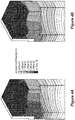
- Figure 4A shows the voltage drop in electron quasi Fermi potential for the cell shown in Figure 3 but without the current spread region 130
- Figure 4B shows the voltage drop for the cell shown in Figure 3 with the current spread region 130.
- Figure 4B demonstrates that the semiconductor device with the current spread region 130 has better channel current spreading which yields a lower voltage drop for the device.
- the amount of on-resistance improvement corresponds to the level of doping of the current spread region 130, as previously explained herein.
- Figures 5 through 9 illustrate respective plan views of additional embodiments of the current spread region 130.
- the body and source regions 104, 106 are obscured / out of view in Figures 5 through 9 to provide an unobstructed view of the current spread region 130 in each case.
- the semiconductor devices shown in Figures 5 through 9 may have the same or similar epitaxial layer stack construction as shown in Figures 1A-1B and Figure 3 .
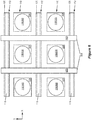
- the current spread region 130 abuts the sidewall 132 of each spicular-shaped field plate structure 110 and is confined by adjacent ones of the stripe-shaped gate structures 112.
- the current spread region 130 may be formed by implanting a dopant species of the first conductivity type through the body region 104 using the same lithography mask for forming the source region 106. Hence, no additional lithography process is needed and no degradation of the edge termination blocking capability of the device occurs. That is, the existing source lithography is used and only an additional implant step is needed over the whole area to form the current spread region 130.
- the implanted dopant species is activated, e.g., by annealing to form the current spread region 130.
- the current spread region 130 is formed as stripes 600 which extend lengthwise (direction 'y' in Figure 6 ) between adjacent ones of the spicular-shaped field plate structures 110 and intersect neighboring ones of the stripe-shaped gate structures 112.
- the stripe-shaped gate structures 112 run orthogonal (direction 'x' in Figure 6 ) to the lengthwise extension direction of the stripes 600 of the current spread region 130.
- the current spread region 130 may be formed by, after forming the source region 106, forming an additional lithography mask on the semiconductor substrate 100 and which has stripe-shaped openings extending lengthwise (direction 'y' in Figure 6 ) between adjacent ones of the spicular-shaped field plate structures 110 and intersect neighboring ones of the stripe-shaped gate structures 112, and implanting a dopant species of the first conductivity type through the body region 104 using the additional lithography mask with the stripe-shaped openings. While an additional lithography step is needed according to this embodiment, the current spread region 200/600 is formed only in targeted regions, minimizing impact on breakdown voltage, DIBL (drain-induced barrier lowering) and avalanche.
- DIBL drain-induced barrier lowering
- the stripe-shaped gate structures 112 have lateral extensions 700 which extend partly between adjacent ones of the spicular-shaped field plate structures110 so that a gap 702 is present between each lateral extension 700 and a neighboring one of the stripe-shaped gate structures 110.
- the stripe-shaped gate structures 112 may extend partly along an orthogonal direction (direction 'y' in Figure 7 ) but not from one stripe-shaped gate trench structure 112 to the adjacent (neighboring) stripe-shaped gate trench structure 112 which run lengthwise in direction 'x' in Figure 7 .
- the current spread region 130 is confined to the gaps 702 in the lateral extensions 700 of the stripe-shaped gate structures 112.
- the current spread region 130 may be formed by, after forming the source region 106, forming an additional lithography mask on the semiconductor substrate 100 and which has openings over the gaps 702 between the lateral extensions 700 of the stripe-shaped gate structures 112. A dopant species of the first conductivity type is then implanted through the body region 104 using the additional lithography mask having the openings over the gaps 702.
- the embodiment illustrated in Figure 7 requires an additional lithography step and forms the current spread region 130 only in targeted regions to minimize impact on breakdown voltage, DIBL and avalanche.
- the embodiment illustrated in Figure 7 provides the additional flexibility for the FOMg/FOMgd/Ron trade-off previously described herein in connection with Tables 1 and 2.
- the current spread region 130 is formed as stripes 800 which extend lengthwise (direction 'y' in Figure 8 ) between adjacent ones of the spicular-shaped field plate structures 110 and terminate before reaching neighboring ones of the stripe-shaped gate structures 112.
- the stripe-shaped gate structures 112 run orthogonal (direction 'x' in Figure 8 ) to the lengthwise extension direction of the stripes 800 of the current spread region 130.
- the current spread region 130 may be formed by forming stripe-shaped grooves in the semiconductor substrate 100 which extend lengthwise (direction 'y' in Figure 8 ) between adjacent ones of the spicular-shaped field plate structures 110 and terminate before reaching neighboring ones of the stripe-shaped gate structures 112, and implanting a dopant species of the first conductivity type into the stripe-shaped grooves. Like the embodiments illustrated in Figures 6 and 7 , the embodiment illustrated in Figure 8 also forms the current spread region 130 in targeted regions to minimize impact on breakdown voltage, DIBL and avalanche.
- a lower ion implantation energy may be used to form the stripes 800 of the current spread region 130 since the implantation is not done through the body region 104 or only through a partial thickness of the body region 104, thereby narrowing the distribution of the implanted ion depth.
- the current spread ion implantation is not done over the stripe-shaped gate structures 112. Instead, open contact grooves are used to do a tilted implant from the sidewall 132 of the spicular-shaped field plate trenches 110 without requiring an extra lithography step.
- the contact grooves can be opened over the entire length of the field plate trenches 122.
- the current spread ion implantation can be performed using a twin-mode tilted implant on both sides of the spicular-shaped field plate trenches 110, as indicated by the dashed lines in Figure 8 .
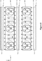
- the current spread region 130 is defined by contact grooves 900 which run parallel (direction 'x' in Figure 9 ) with the stripe-shaped gate structures 112 and are aligned with the rows of spicular-shaped field plate structures 110.
- the current spread region 130 may be formed by etching the contact grooves 900 into the semiconductor substrate 100, each contact groove having unetched stripe-shaped regions 902 (direction 'y' in Figure 9 ) in parallel with one another, and implanting a dopant species of the first conductivity type into the contact grooves 900.
- a relatively low energy ion implantation may be used to form the current spread region 130 since the implant is done through contact grooves 900. No extra lithography step is needed, and only a subsequent thermal budget for activating a highly-doped body contact region acts on the current spread implant, allowing for precise definition of the implanted ion depth.
- the contact grooves 900 have a stripe-like shape with bars 902 for easier fill with a metal, metal alloy, etc. to form a source/body contact 904, with 0° or tilted implant into the contact grooves 900 to form the current spread region 130.
- the current spread region 130 is not shown in Figure 9 , but the implantation process for the current spread region 130 is indicated by dashed lines in Figure 9 .
- each contact groove 900 By keeping unetched stripe-shaped regions 902 in each contact groove 900, there is no edge of contact which is better for lithographic processing in that identical open areas over the entire chip (die) provides for better control.
- the current spread ion implantation can be performed using a twin-mode tilted implant on both sides of the contact grooves 900.
- the rows of spicular-shaped field plate structures 110 may be shifted with respect to one another so that the power transistor cell may have, for example, a hexagonal grid-like layout when viewed from above and some gate connections may be omitted so that in the top layout view, the stripe-shaped gate structures 112 run in zig-zag patterns over the chip.
- the stripe-shaped gate structures 112 may run lengthwise in straight or zig-zag patterns.
Landscapes
- Insulated Gate Type Field-Effect Transistor (AREA)
- Electrodes Of Semiconductors (AREA)
- Junction Field-Effect Transistors (AREA)
Abstract
Description
- Power MOSFETs (metal-oxide semiconductor field-effect transistor) typically have a field-plate for charge compensation, thereby offering a significant improvement in area-specific on resistance (RxA). Some power transistor cell designs use a stripe-trench for the field plates, with the gate electrode in the same stripe-shaped trench as the field electrode. Other power transistor cell designs place the field plate in a deep needle-shaped trench in the center of the cell and surround the needle-shaped trench with a separate trench which includes the gate electrode. The increased semiconductor mesa area between the deep needle-shaped trench in the center of the cell and the surrounding gate trench is expected to provide even lower overall on-resistance.
- Different from stripe-shaped field plate designs, cell designs with a needle-shaped field plate trench at the center of the cell do not integrate the gate electrode in the field plate trench. Instead, the gate electrode is moved to a separate trench which surrounds the needle-shaped field plate trench in the center of the cell. To reduce the area-specific on-resistance, the gate trench must now form a grid across the chip (die) to use the additional semiconductor mesa area for current conduction.
- As such, cell designs with a needle-shaped field plate trench at the center of the cell offer lower area-specific on-resistance and also reduce the output charge of the device which contributes significantly to overall losses in targeted applications. However, conventional cell designs with a needle-shaped field plate trench do not allow for an easy reduction of gate charge and gate-drain charge, as the overall gate area is significantly increased compared to a gate-stripe layout.
- Thus, there is a need for a cell design with a needle-shaped field plate trench and lower gate charge and gate-drain charge with reduced impact on area-specific on-resistance.
- According to the invention, a semiconductor device is provided that comprises: a semiconductor substrate comprising a drift region of a first conductivity type, a body region of a second conductivity type formed above the drift region, and a source region of the first conductivity type separated from the drift region by the body region; rows of spicular-shaped field plate structures formed in the semiconductor substrate, the spicular-shaped field plate structures extending through the source region and the body region into the drift region; stripe-shaped gate structures formed in the semiconductor substrate and separating adjacent rows of the spicular-shaped field plate structures; and a current spread region of the first conductivity type formed below the body region in semiconductor mesas between adjacent ones of the spicular-shaped field plate structures and which are devoid of the stripe-shaped gate structures, the current spread region configured to increase channel current distribution in the semiconductor mesas.
- The current spread region may abut a sidewall of the spicular-shaped field plate structures.
- Separately or in combination, the current spread region may be confined by adjacent ones of the stripe-shaped gate structures.
- Separately or in combination, the current spread region may laterally extend from a sidewall of each spicular-shaped field plate structure to a sidewall of the adjacent stripe-shaped gate structure.
- Separately or in combination, the current spread region may comprise stripes which extend lengthwise between adjacent ones of the spicular-shaped field plate structures and intersect neighboring ones of the stripe-shaped gate structures.
- Separately or in combination, the stripe-shaped gate structures may have lateral extensions which extend partly between adjacent ones of the spicular-shaped field plate structures so that a gap is present between each lateral extension and a neighboring one of the stripe-shaped gate structures, and the current spread region may be confined to the gaps between the lateral extensions of the stripe-shaped gate structures and the neighboring stripe-shaped gate structures.
- Separately or in combination, the current spread region may comprise stripes which extend lengthwise between adjacent ones of the spicular-shaped field plate structures and terminate before reaching neighboring ones of the stripe-shaped gate structures.
- Separately or in combination, the current spread region may be defined by contact grooves which run parallel with the stripe-shaped gate structures and are aligned with the rows of spicular-shaped field plate structures.
- Separately or in combination, the spicular-shaped field plate structures may each comprise a field electrode disposed in a trench and a field dielectric insulating the field electrode from the semiconductor substrate.
- Separately or in combination, the spicular-shaped field plate structures may each comprise a connection region connected to and which is narrower than the field electrode, the field electrode being located deeper in the trench than the connection region, and the current spread region may be formed adjacent the connection region of the spicular-shaped field plate structures.
- Separately or in combination, the current spread region may have a peak doping concentration at a depth in the semiconductor substrate which is shallower than a bottom of the stripe-shaped gate structures.
- According to the invention, a method of producing a semiconductor device is provided that comprises: forming a drift region of a first conductivity type, a body region of a second conductivity type formed above the drift region, and a source region of the first conductivity type separated from the drift region by the body region in a semiconductor substrate; forming rows of spicular-shaped field plate structures in the semiconductor substrate, the spicular-shaped field plate structures extending through the source region and the body region into the drift region; forming stripe-shaped gate structures in the semiconductor substrate and separating adjacent rows of the spicular-shaped field plate structures; and forming a current spread region of the first conductivity type below the body region in semiconductor mesas between adjacent ones of the spicular-shaped field plate structures and which are devoid of the stripe-shaped gate structures, the current spread region configured to increase channel current distribution in the semiconductor mesas.
- Forming the current spread region may comprise implanting a dopant species of the first conductivity type through the body region using a same lithography mask for forming the source region.
- Separately or in combination, forming the current spread region may comprise: after forming the source region, forming a lithography mask on the semiconductor substrate and which has stripe-shaped openings which extend lengthwise between adjacent ones of the spicular-shaped field plate structures and intersect neighboring ones of the stripe-shaped gate structures; and implanting a dopant species of the first conductivity type through the body region using the lithography mask with the stripe-shaped openings.
- Separately or in combination, the stripe-shaped gate structures may have lateral extensions which extend partly between adjacent ones of the spicular-shaped field plate structures so that a gap is present between each lateral extension and a neighboring one of the stripe-shaped gate structures, and forming the current spread region may comprise: after forming the source region, forming a lithography mask on the semiconductor substrate and which has openings over the gaps between the lateral extensions of the stripe-shaped gate structures and the neighboring stripe-shaped gate structures; and implanting a dopant species of the first conductivity type through the body region using the lithography mask with the openings over the gaps.
- Separately or in combination, forming the current spread region may comprise: forming stripe-shaped grooves in the semiconductor substrate which extend lengthwise between adjacent ones of the spicular-shaped field plate structures and terminate before reaching neighboring ones of the stripe-shaped gate structures; and implanting a dopant species of the first conductivity type into the stripe-shaped grooves.
- Separately or in combination, forming the current spread region may comprise: etching contact grooves into the semiconductor substrate which run parallel with the stripe-shaped gate structures and are aligned with the rows of spicular-shaped field plate structures, each contact groove having unetched stripe-shaped regions in parallel with one another; and implanting a dopant species of the first conductivity type into the contact grooves.
- Separately or in combination, forming the rows of spicular-shaped field plate structures may comprise: etching rows of trenches in the semiconductor substrate; and forming a field electrode and a field dielectric insulating the field electrode from the semiconductor substrate in each trench.
- Separately or in combination, the spicular-shaped field plate structures may each comprise a connection region connected to and which is narrower than the field electrode, the field electrode being located deeper in the trench than the connection region, and forming the current spread region may comprise forming the current spread region adjacent the connection region of the spicular-shaped field plate structures.
- Those skilled in the art will recognize additional features and advantages upon reading the following detailed description, and upon viewing the accompanying drawings.
- The elements of the drawings are not necessarily to scale relative to each other. Like reference numerals designate corresponding similar parts. The features of the various illustrated embodiments can be combined unless they exclude each other.
- Embodiments are depicted in the drawings and are detailed in the description which follows.
-
Figure 1A illustrates a partial cross-sectional view of a power transistor cell with a current spread region, andFigure 1B illustrates a different partial cross-sectional view of the same power transistor cell. -
Figure 2A shows the voltage drop for the cell shown inFigures 1A and 1B but without the current spread region, andFigure 2B shows the voltage drop for the cell shown inFigures 1A and 1B with the current spread region. -
Figure 3 illustrates a partial cross-sectional view of another power transistor cell with a current spread region. -
Figure 4A shows the voltage drop for the cell shown inFigure 3 but without the current spread region, andFigure 4B shows the voltage drop for the cell shown inFigure 3 with the current spread region. -
Figures 5 through 9 illustrate respective plan views of additional embodiments of the current spread region. - The embodiments described herein provide a power transistor cell design with a needle-shaped field plate trench and lower gate charge and gate-drain charge with reduced impact on area-specific on-resistance. The power transistor device has rows of spicular-shaped field plate structures formed in the semiconductor substrate and stripe-shaped gate structures separating adjacent rows of the spicular-shaped field plate structures. A current spread region is formed in semiconductor mesas between adjacent ones of the spicular-shaped field plate structures and which are devoid of the stripe-shaped gate structures. The current spread region is configured to increase channel current distribution in the semiconductor mesas, thereby lowering gate charge and gate-drain charge with little to no adverse impact on area-specific on-resistance. The terms "needle-shaped" and "spicular-shaped" are used interchangeably herein to describe a trench structure formed in a semiconductor substrate and having a small or narrow circumference or width in proportion to its height / depth in the substrate, as opposed to a stripe-shaped trench structure which is longer than it is deeper.
-
Figure 1A illustrates a partial cross-sectional view of a power transistor cell, andFigure 1B illustrates a different partial cross-sectional view of the same power transistor cell. A semiconductor device may include dozens, 100s, 1000s or even more of the power transistor cells integrated on the same die and electrically coupled in parallel to form a power transistor. The semiconductor device may be a power MOSFET, an IGBT (insulated gate bipolar transistor), a HEMT (high-electron mobility transistor), etc. In each case, the semiconductor device includes asemiconductor substrate 100 comprising adrift region 102 of a first conductivity type, abody region 104 of a second conductivity type formed above thedrift region 102, and asource region 106 of the first conductivity type separated from thedrift region 102 by thebody region 104. Thedrain region 108 of the semiconductor device may be disposed at the opposite side of thesemiconductor substrate 100 as thesource region 106. The term "source region" as used herein is intended to mean the source region of a power MOSFET or HEMT, or the emitter region of an IGBT. Similarly, term "drain region" as used herein is intended to mean the drain region of a power MOSFET or HEMT, or the collector region of an IGBT. - In the case of an n-channel device, the first conductivity type is n-type and the second conductivity type is p-type. Conversely in the case of a p-channel device, the first conductivity type is p-type and the second conductivity type is n-type.
- For either an n-channel or p-channel device, the semiconductor device includes rows of spicular-shaped
field plate structures 110 formed in thesemiconductor substrate 100. The semiconductor device also includes stripe-shaped gate structures 112 formed in thesemiconductor substrate 100 and separating adjacent rows of the spicular-shapedfield plate structures 110. An interlayer dielectric 114 such as an oxide, nitride etc. insulates electrical connections to the stripe-shaped gate structures 112 from electrical connections to the spicular-shapedfield plate structures 110, and a highlydoped contact region 115 may be provided for electrically contacting thebody region 104. As mentioned above, only part of one transistor cell is shown inFigures 1A and 1B . However,Figures 5 through 9 show different embodiments of the semiconductor device and in which stripe-shaped gate structures 112 separate adjacent rows of spicular-shapedfield plate structures 110. - The spicular-shaped
field plate structures 110 extend through thesource region 106 and thebody region 104 into thedrift region 102. The main current flow path of the device shown inFigures 1A and 1B is vertical, from thesource region 106 to thedrain region 108 and controlled by a voltage applied to agate electrode 116 of the stripe-shaped gate structures 112.Field plates 118 of the spicular-shapedfield plate structures 110 shape the electric field that builds up in thesemiconductor substrate 100 when the device is in a blocking state, protecting thegate dielectric 120 and enhancing the breakdown characteristics of the device. - The spicular-shaped
field plate structures 110 each include afield electrode 118 disposed in atrench 122 and afield dielectric 124 insulating thefield electrode 118 from thesemiconductor substrate 100. The stripe-shapedgate structures 112 each include agate electrode 116 disposed in atrench 126 separate from thefield plate trenches 122 and agate dielectric 120 insulating thegate electrode 116 from thesemiconductor substrate 100. The stripe-shapedgate structures 112 run along at least two sides of the needle-shaped field plate structures 110 (e.g. parallel but not orthogonal), or may even run along all four sides of the needle-shapedfield plate structures 110 but not in continuous grids. That is, even if the stripe-shapedgate structures 112 run along all four sides of the needle-shapedfield plate structures 100, there is a break or gap in some of the stripe-shapedgate structures 112 such that there aresemiconductor mesas 128 located between adjacent ones of the spicular-shapedfield plate structures 110 and which are devoid of the stripe-shapedgate structures 112. - Due to the use of spicular-shaped
field plate structures 110 and stripe-shapedgate structures 112, the power transistor cell design has lower overall on-resistance. However, not all of the semiconductor material between adjacent spicular-shapedfield plate structures 110 is influenced by the gate voltage, since thegate trenches 126 are formed as stripes and therefore do not completely surround individual ones of the spicular-shapedfield plate structures 110 as explained above. - To reduce the area-specific on-resistance of the semiconductor device while also lowering the gate charge and gate-drain charge, the device also includes a
current spread region 130 of the first conductivity type formed below thebody region 104 in thesemiconductor mesas 128 located between adjacent ones of the spicular-shapedfield plate structures 110 and which are devoid of the stripe-shapedgate structures 112. Thecurrent spread region 130 has a higher average doping concentration than thedrift region 102, and therefore increases the channel current distribution in thesemiconductor mesas 128 which are devoid of the stripe-shapedgate structures 112. - The
current spread region 130 distributes the channel current in thesemiconductor mesas 128 into which thegate trenches 126 do not extend. By including the current spread region at least in thesemiconductor mesas 128 located between adjacent ones of the spicular-shapedfield plate structures 110 and which are devoid of the stripe-shapedgate structures 112, a less resistive region of the first conductivity type is provided just below thebody region 104 in thesemesa regions 128, allowing the channel current to spread out laterally in a more distributed manner as the channel current flows into the upper part of thedrift region 102 and vertically toward thedrain region 108. -
Figure 2A shows the voltage drop in electron quasi Fermi potential for the cell shown inFigures 1A and 1B but without thecurrent spread region 130, andFigure 2B shows the voltage drop for the cell shown inFigures 1A and 1B with thecurrent spread region 130.Figure 2B demonstrates that the semiconductor device with thecurrent spread region 130 has better channel current spreading which yields a lower voltage drop for the device. For example, in some cases, thecurrent spread region 130 may improve the area-specific on resistance (RxA) from 30 mill-Ohm mm2 down to 27.3 mill-Ohm mm2 or even lower while the breakdown voltage increases slightly. The amount of on-resistance improvement is based on the increase in doping of thecurrent spread region 130. In one embodiment, thecurrent spread region 130 has a graded doping profile that increases towards thebody region 104 for lowering the on-resistance. - However, a practical limitation on the doping concentration of the
current spread region 130 is set by a corresponding reduction in VFPmax. This requires a careful optimization due to the changed field distribution compared to a device with a continuous gate grid surrounding the field plate structures, resulting in higher breakdown voltage (BVDSS) and VFPmax for the same epitaxial layer stack. - VFPmax is not directly measurable at the device, but can be determined on a test structure where the
field electrode 118 is separated from the source. With such a test structure, the potential of thefield electrode 118 can be changed. By varying the potential of thefield electrode 118, the blocking capability of the device changes. Therefore, the breakdown voltage may first rise with increasing the field electrode potential, reaching a maximum value which is defined as VFPmax. A further increase of the potential at thefield electrode 118 results in a fast decline of the breakdown voltage, meaning the characteristic breakdown voltage over VFP is typically asymmetric. To provide a stable device behaviour that is robust against process tolerances, the device may be designed in a way that VFPmax is always positive. - If the field electrode potential is kept constant, e.g., typically at zero Volts as the
field electrode 118 is connected to source potential, an increase of the doping yields the same behaviour - first a rising breakdown voltage and later a declining one. So VFPmax is a measure of how far away the device is from the theoretical maximum doping. VFPmax is also an indicator value for how much charge might be generated at the field-oxide interface in avalanche events. In such operation modes, some hot-carrier injection occurs at this interface and the generated charge does the same as an increased field electrode potential. To compare the performance including on-resistance of differently designed structures, not only the breakdown voltage but also VFPmax should be comparable. - Table 1 below demonstrates area-specific on-resistance (Ron X A) measured in milliohm per mm2, VFPmax measured in Volts, breakdown voltage (BVDSS) measured in Volts, FOM (figure of merit) for gate charge (FOMg) which is the product of on-resistance and gate charge and measured in milliohm-nC, and FOM for gate-drain charge (FOMgd) which is the product of on-resistance and gate-drain charge and also measured in milliohm-nC, for different cell designs including the cell design illustrated in
Figures 1A and 1B .Table 1 Ron X A (milliohm mm2) BVDSS (V) VFPmax (V) FOMg (milliohm-nC) FOMgd (milliohm-nC) Cell Design 1 25 106.3 3 141.9 23.6 Cell Design 2 30 106.6 4.9 96.0 16.5 Cell Design 3 28.3 106.9 2.6 92.5 17.5 Cell Design 4 27.3 106.9 0.4 90.2 17.9 Cell Design 5 26.5 104.1 -2.2 90.0 19.3 Cell Design 6 25.9 97.4 -5.8 88.5 20.7 - The cell designs each have a spicular-shaped field plate structure at the center of the cell and the same epitaxial layer stack. However, 'Cell Design 1' has a gate trench which surrounds the needle-shaped field trench in a closed (continuous) grid-like manner. 'Cell Design 2' is the cell shown in
Figures 1A and 1B , but without thecurrent spread region 130. 'Cell Design 3' is the cell shown inFigures 1A and 1B with thecurrent spread region 130 formed by an implantation dose of 5e11cm-2. 'Cell Design 4' is the cell shown inFigures 1A and 1B with thecurrent spread region 130 formed by an implantation dose of 1e12cm-2. 'Cell Design 5' is the cell shown inFigures 1A and 1B with thecurrent spread region 130 formed by an implantation dose of 1.5e12cm-2. 'Cell Design 6' is the cell shown inFigures 1A and 1B with thecurrent spread region 130 formed by an implantation dose of 2e12cm-2. - Setting the implantation dose for the
current spread region 130 too high yields negative VFPmax and decreases BVDSS, where higher implantation dose translates to increased doping. The doping concentration of thecurrent spread region 130 depends on the device construction and targeted voltage class. Hence, thecurrent spread region 130 may have different base doping levels for different cell constructions and voltage classes. - The doping level of the
current spread region 130 effects the on-state resistance (Ron) of the device. The on-state resistance Ron corresponds to a defined amount of dopants per area and stretches to a certain depth, so the change in doping in thecurrent spread region 130 can be identified as compared to the base doping of thedrift region 102 even though bothregions - The
current spread region 130 is formed under thebody region 104 of the device, but preferably not too far under thegate trenches 126. If thecurrent spread region 130 extends too far under thegate trenches 126, the electric field will increase at the bottom of thegate trenches 126 which can lead to gate dielectric degradation and eventually breakdown. Thegate dielectric 120 may be thicker at the bottom of thegate trenches 126 to mitigate this risk. Ideally, thecurrent spread region 130 does not extend at all under thegate trenches 130. However, this may not be practical. Hence, thecurrent spread region 130 may have some lateral extension under thegate trenches 126 which may be difficult to avoid. In the case of a thick bottom oxide, adeeper gate trench 126 may be used so that thegate electrode 116 is long enough to fully open the device channel. - The
current spread region 130 has a higher average doping concentration than thedrift region 102 as explained above. Thecurrent spread region 130 therefore has lower resistance that thedrift region 102 , allowing the channel current to spread (distribute) faster in multiple dimensions. The maximum doping concentration of thecurrent spread region 130 ideally is at the junction with thebody region 104, but this may not be practical. In one embodiment, the peak doping concentration of thecurrent spread region 130 is at a depth in thesemiconductor substrate 100 which is shallower than the bottom of the stripe-shapedgate structures 112. The peak doping concentration of thecurrent spread region 130 may be 1.5x to 5x higher than the average doping concentration, e.g., 2x to 4x higher. - By providing the
current spread region 130 below thebody region 104 in thesemiconductor mesas 128 located between adjacent ones of the spicular-shapedfield plate structures 110 and which are devoid of the stripe-shapedgate structures 112, the spicular-shapedfield plate structures 110 may be arranged in a grid whereas thegate structures 112 may be formed as stripes which run along two sides of each needle-shaped field plate 110 (e.g. parallel but not orthogonal) or even all 4 sides but without forming a closed (continuous) grid. Thecurrent spread region 130 increases the channel current distribution in thesemiconductor mesas 128 between adjacent ones of the spicular-shapedfield plate structures 110 and which are devoid of the stripe-shapedgate structures 112 and thereby lower gate charge and gate-drain charge, with little to no adverse impact on area-specific on-resistance. - Described next are various embodiments for the position, shape and formation of the
current spread region 130 within each cell of a power semiconductor device. Thecurrent spread region 130 may abut asidewall 132 of the spicular-shapedfield plate structures 110, e.g., as shown inFigures 1A and 1B . Thecurrent spread region 130 may laterally extend from asidewall 132 of each spicular-shapedfield plate structure 110 to asidewall 134 of the adjacent stripe-shapedgate structure 112, also as shown inFigures 1A and 1B . -
Figure 3 illustrates a partial cross-sectional view of a power transistor cell according to another embodiment. The power transistor cell embodiment shown inFigure 3 is similar to the embodiment shown inFigures 1A and 1B . Different, however, the spicular-shapedfield plate structures 110 each have aconnection region 300 connected to and which is narrower than thefield electrode 118. Theconnection region 300 is provided in the upper part of thefield plate trenches 122, and provides a point of electrical connection to thefield electrode 118 which is located lower in thefield plate trenches 122 than theconnection region 300. According to this embodiment, thecurrent spread region 130 is formed adjacent theconnection region 300 of the spicular-shapedfield plate structures 100. Also, a smaller semiconductor mesa width (Wm) is realized by using theconnection region 300 to contact the wider buriedfield plates 118. Hence, the mesa doping may be higher while the width into which the channel current spreads is lower. - Table 2 below demonstrates area-specific on-resistance (Ron X A), VFPmax, breakdown voltage (BVDSS), FOM (figure of merit) for gate charge (FOMg), and FOM for gate-drain charge (FOMgd), for different cell designs including the cell design illustrated in
Figure 3 .Table 2 Ron X A (milliohm mm2) BVDSS (V) VFPmax (V) FOMg (milliohm-nC) FOMgd (milliohm-nC) Cell Design 1 20 100.2 5 117.2 20.8 Cell Design 2 22.6 100.5 5 82.5 15.3 Cell Design 3 21.8 100.5 3.3 82.2 16.8 Cell Design 4 21.3 100.4 1.3 80.4 17.3 Cell Design 5 21 98.6 -1.4 80.2 18.4 Cell Design 6 20.6 93.7 -4.2 80.3 20.1 - The cell design simulation parameters summarized in Table 2 are identical to those summarized in Table 1, except the 'Cell Design 3' through 'Cell Design 6' correspond to the cell embodiment shown in
Figure 3 instead of the cell embodiment ofFigures 1A and 1B . Comparing the simulation results in Tables 1 and 2 for 'Cell Design 3' through 'Cell Design 6' shows that the cell embodiment illustrated inFigure 3 allows for a more efficient lateral spreading of the channel current which results in less negative impact on the on-resistance as compared to the cell embodiment illustrated inFigures 1A and 1B . -
Figure 4A shows the voltage drop in electron quasi Fermi potential for the cell shown inFigure 3 but without thecurrent spread region 130, andFigure 4B shows the voltage drop for the cell shown inFigure 3 with thecurrent spread region 130. LikeFigure 2B ,Figure 4B demonstrates that the semiconductor device with thecurrent spread region 130 has better channel current spreading which yields a lower voltage drop for the device. The amount of on-resistance improvement corresponds to the level of doping of thecurrent spread region 130, as previously explained herein. -
Figures 5 through 9 illustrate respective plan views of additional embodiments of thecurrent spread region 130. The body andsource regions Figures 5 through 9 to provide an unobstructed view of thecurrent spread region 130 in each case. The semiconductor devices shown inFigures 5 through 9 may have the same or similar epitaxial layer stack construction as shown inFigures 1A-1B andFigure 3 . - In
Figure 5 , thecurrent spread region 130 abuts thesidewall 132 of each spicular-shapedfield plate structure 110 and is confined by adjacent ones of the stripe-shapedgate structures 112. Thecurrent spread region 130 may be formed by implanting a dopant species of the first conductivity type through thebody region 104 using the same lithography mask for forming thesource region 106. Hence, no additional lithography process is needed and no degradation of the edge termination blocking capability of the device occurs. That is, the existing source lithography is used and only an additional implant step is needed over the whole area to form thecurrent spread region 130. - However, a relatively high energy implant is needed to form the
current spread region 130 underneath thebody region 104, which may result in a large variation of the implanted ion depth. The implanted dopant species is activated, e.g., by annealing to form thecurrent spread region 130. - In
Figure 6 , thecurrent spread region 130 is formed asstripes 600 which extend lengthwise (direction 'y' inFigure 6 ) between adjacent ones of the spicular-shapedfield plate structures 110 and intersect neighboring ones of the stripe-shapedgate structures 112. In one embodiment, the stripe-shapedgate structures 112 run orthogonal (direction 'x' inFigure 6 ) to the lengthwise extension direction of thestripes 600 of thecurrent spread region 130. - The
current spread region 130 may be formed by, after forming thesource region 106, forming an additional lithography mask on thesemiconductor substrate 100 and which has stripe-shaped openings extending lengthwise (direction 'y' inFigure 6 ) between adjacent ones of the spicular-shapedfield plate structures 110 and intersect neighboring ones of the stripe-shapedgate structures 112, and implanting a dopant species of the first conductivity type through thebody region 104 using the additional lithography mask with the stripe-shaped openings. While an additional lithography step is needed according to this embodiment, the current spread region 200/600 is formed only in targeted regions, minimizing impact on breakdown voltage, DIBL (drain-induced barrier lowering) and avalanche. - In
Figure 7 , the stripe-shapedgate structures 112 havelateral extensions 700 which extend partly between adjacent ones of the spicular-shaped field plate structures110 so that agap 702 is present between eachlateral extension 700 and a neighboring one of the stripe-shapedgate structures 110. For example, the stripe-shapedgate structures 112 may extend partly along an orthogonal direction (direction 'y' inFigure 7 ) but not from one stripe-shapedgate trench structure 112 to the adjacent (neighboring) stripe-shapedgate trench structure 112 which run lengthwise in direction 'x' inFigure 7 . Thecurrent spread region 130 is confined to thegaps 702 in thelateral extensions 700 of the stripe-shapedgate structures 112. - The
current spread region 130 may be formed by, after forming thesource region 106, forming an additional lithography mask on thesemiconductor substrate 100 and which has openings over thegaps 702 between thelateral extensions 700 of the stripe-shapedgate structures 112. A dopant species of the first conductivity type is then implanted through thebody region 104 using the additional lithography mask having the openings over thegaps 702. Like the embodiment illustrated inFigure 6 , the embodiment illustrated inFigure 7 requires an additional lithography step and forms thecurrent spread region 130 only in targeted regions to minimize impact on breakdown voltage, DIBL and avalanche. The embodiment illustrated inFigure 7 provides the additional flexibility for the FOMg/FOMgd/Ron trade-off previously described herein in connection with Tables 1 and 2. - In
Figure 8 , thecurrent spread region 130 is formed asstripes 800 which extend lengthwise (direction 'y' inFigure 8 ) between adjacent ones of the spicular-shapedfield plate structures 110 and terminate before reaching neighboring ones of the stripe-shapedgate structures 112. In one embodiment, the stripe-shapedgate structures 112 run orthogonal (direction 'x' inFigure 8 ) to the lengthwise extension direction of thestripes 800 of thecurrent spread region 130. - The
current spread region 130 may be formed by forming stripe-shaped grooves in thesemiconductor substrate 100 which extend lengthwise (direction 'y' inFigure 8 ) between adjacent ones of the spicular-shapedfield plate structures 110 and terminate before reaching neighboring ones of the stripe-shapedgate structures 112, and implanting a dopant species of the first conductivity type into the stripe-shaped grooves. Like the embodiments illustrated inFigures 6 and7 , the embodiment illustrated inFigure 8 also forms thecurrent spread region 130 in targeted regions to minimize impact on breakdown voltage, DIBL and avalanche. However, by forming the stripe-shaped grooves in thesemiconductor substrate 100 which run transverse to the stripe-shapedgate structures 112, a lower ion implantation energy may be used to form thestripes 800 of thecurrent spread region 130 since the implantation is not done through thebody region 104 or only through a partial thickness of thebody region 104, thereby narrowing the distribution of the implanted ion depth. - The current spread ion implantation is not done over the stripe-shaped
gate structures 112. Instead, open contact grooves are used to do a tilted implant from thesidewall 132 of the spicular-shapedfield plate trenches 110 without requiring an extra lithography step. The contact grooves can be opened over the entire length of thefield plate trenches 122. The current spread ion implantation can be performed using a twin-mode tilted implant on both sides of the spicular-shapedfield plate trenches 110, as indicated by the dashed lines inFigure 8 . - In
Figure 9 , thecurrent spread region 130 is defined bycontact grooves 900 which run parallel (direction 'x' inFigure 9 ) with the stripe-shapedgate structures 112 and are aligned with the rows of spicular-shapedfield plate structures 110. Thecurrent spread region 130 may be formed by etching thecontact grooves 900 into thesemiconductor substrate 100, each contact groove having unetched stripe-shaped regions 902 (direction 'y' inFigure 9 ) in parallel with one another, and implanting a dopant species of the first conductivity type into thecontact grooves 900. - A relatively low energy ion implantation may be used to form the
current spread region 130 since the implant is done throughcontact grooves 900. No extra lithography step is needed, and only a subsequent thermal budget for activating a highly-doped body contact region acts on the current spread implant, allowing for precise definition of the implanted ion depth. Thecontact grooves 900 have a stripe-like shape withbars 902 for easier fill with a metal, metal alloy, etc. to form a source/body contact 904, with 0° or tilted implant into thecontact grooves 900 to form thecurrent spread region 130. Thecurrent spread region 130 is not shown inFigure 9 , but the implantation process for thecurrent spread region 130 is indicated by dashed lines inFigure 9 . By keeping unetched stripe-shapedregions 902 in eachcontact groove 900, there is no edge of contact which is better for lithographic processing in that identical open areas over the entire chip (die) provides for better control. The current spread ion implantation can be performed using a twin-mode tilted implant on both sides of thecontact grooves 900. - In general, the rows of spicular-shaped
field plate structures 110 may be shifted with respect to one another so that the power transistor cell may have, for example, a hexagonal grid-like layout when viewed from above and some gate connections may be omitted so that in the top layout view, the stripe-shapedgate structures 112 run in zig-zag patterns over the chip. Hence, the stripe-shapedgate structures 112 may run lengthwise in straight or zig-zag patterns. - Terms such as "first", "second", and the like, are used to describe various elements, regions, sections, etc. and are also not intended to be limiting. Like terms refer to like elements throughout the description.
- As used herein, the terms "having", "containing", "including", "comprising" and the like are open ended terms that indicate the presence of stated elements or features, but do not preclude additional elements or features. The articles "a", "an" and "the" are intended to include the plural as well as the singular, unless the context clearly indicates otherwise.
- It is to be understood that the features of the various embodiments described herein may be combined with each other, unless specifically noted otherwise.
- Although specific embodiments have been illustrated and described herein, it will be appreciated by those of ordinary skill in the art that a variety of alternate and/or equivalent implementations may be substituted for the specific embodiments shown and described without departing from the scope of the present invention. This application is intended to cover any adaptations or variations of the specific embodiments discussed herein. Therefore, it is intended that this invention be limited only by the claims and the equivalents thereof.
Claims (15)
- A semiconductor device, comprising:a semiconductor substrate comprising a drift region of a first conductivity type, a body region of a second conductivity type formed above the drift region, and a source region of the first conductivity type separated from the drift region by the body region;rows of spicular-shaped field plate structures formed in the semiconductor substrate, the spicular-shaped field plate structures extending through the source region and the body region into the drift region;stripe-shaped gate structures formed in the semiconductor substrate and separating adjacent rows of the spicular-shaped field plate structures; anda current spread region of the first conductivity type formed below the body region in semiconductor mesas between adjacent ones of the spicular-shaped field plate structures and which are devoid of the stripe-shaped gate structures, the current spread region configured to increase channel current distribution in the semiconductor mesas.
- The semiconductor device of claim 1, whereinthe current spread region abuts a sidewall of the spicular-shaped field plate structures and/orthe current spread region is confined by adjacent ones of the stripe-shaped gate structures and/orthe current spread region laterally extends from a sidewall of each of the spicular-shaped field plate structures to a sidewall of the adjacent stripe-shaped gate structure.
- The semiconductor device of claim 1, wherein the current spread region comprises stripes which extend lengthwise between adjacent ones of the spicular-shaped field plate structures and intersect neighboring ones of the stripe-shaped gate structures.
- The semiconductor device of claim 1, wherein the stripe-shaped gate structures have lateral extensions which extend partly between adjacent ones of the spicular-shaped field plate structures so that a gap is present between each lateral extension and a neighboring one of the stripe-shaped gate structures, and wherein the current spread region is confined to the gaps between the lateral extensions of the stripe-shaped gate structures and the neighboring stripe-shaped gate structures.
- The semiconductor device of claim 1, wherein the current spread region comprises stripes which extend lengthwise between adjacent ones of the spicular-shaped field plate structures and terminate before reaching neighboring ones of the stripe-shaped gate structures.
- The semiconductor device of claim 1, wherein the current spread region is defined by contact grooves which run parallel with the stripe-shaped gate structures and are aligned with the rows of spicular-shaped field plate structures.
- The semiconductor device of any one of claims 1 to 6, wherein the spicular-shaped field plate structures each comprise a field electrode disposed in a trench and a field dielectric insulating the field electrode from the semiconductor substrate, wherein the spicular-shaped field plate structures each comprise a connection region connected to and which is narrower than the field electrode, the field electrode being located deeper in the trench than the connection region, and wherein the current spread region is formed adjacent the connection region of the spicular-shaped field plate structures.
- The semiconductor device of any one of claims 1 to 7, wherein the current spread region has a peak doping concentration at a depth in the semiconductor substrate which is shallower than a bottom of the stripe-shaped gate structures.
- The semiconductor device of any one of claims 1 to 8, wherein each of the stripe-shaped gate structures comprises a gate electrode disposed in a trench and a gate dielectric insulating the gate electrode from the semiconductor substrate, wherein the current spread region has a lateral extension under the gate trenches, and wherein the gate oxide is thicker at a bottom of the gate trenches.
- A method of producing a semiconductor device, the method comprising:forming a drift region of a first conductivity type, a body region of a second conductivity type formed above the drift region, and a source region of the first conductivity type separated from the drift region by the body region in a semiconductor substrate;forming rows of spicular-shaped field plate structures in the semiconductor substrate, the spicular-shaped field plate structures extending through the source region and the body region into the drift region;forming stripe-shaped gate structures in the semiconductor substrate and separating adjacent rows of the spicular-shaped field plate structures; andforming a current spread region of the first conductivity type below the body region in semiconductor mesas between adjacent ones of the spicular-shaped field plate structures and which are devoid of the stripe-shaped gate structures, the current spread region configured to increase channel current distribution in the semiconductor mesas.
- The method of claim 10, wherein forming the current spread region comprises implanting a dopant species of the first conductivity type through the body region using a same lithography mask for forming the source region.
- The method of claim 10, wherein forming the current spread region comprises:after forming the source region, forming a lithography mask on the semiconductor substrate and which has stripe-shaped openings which extend lengthwise between adjacent ones of the spicular-shaped field plate structures and intersect neighboring ones of the stripe-shaped gate structures; andimplanting a dopant species of the first conductivity type through the body region using the lithography mask with the stripe-shaped openings.
- The method of claim 10, wherein the stripe-shaped gate structures have lateral extensions which extend partly between adjacent ones of the spicular-shaped field plate structures so that a gap is present between each lateral extension and a neighboring one of the stripe-shaped gate structures, and wherein forming the current spread region comprises:after forming the source region, forming a lithography mask on the semiconductor substrate and which has openings over the gaps between the lateral extensions of the stripe-shaped gate structures and the neighboring stripe-shaped gate structures; andimplanting a dopant species of the first conductivity type through the body region using the lithography mask with the openings over the gaps.
- The method of claim 10, wherein forming the current spread region comprises:forming stripe-shaped grooves in the semiconductor substrate which extend lengthwise between adjacent ones of the spicular-shaped field plate structures and terminate before reaching neighboring ones of the stripe-shaped gate structures; andimplanting a dopant species of the first conductivity type into the stripe-shaped grooves, oretching contact grooves into the semiconductor substrate which run parallel with the stripe-shaped gate structures and are aligned with the rows of spicular-shaped field plate structures, each contact groove having unetched stripe-shaped regions in parallel with one another; andimplanting a dopant species of the first conductivity type into the contact grooves.
- The method of claim 10, wherein the current spread region is formed so as to laterally extend from a sidewall of each of the spicular-shaped field plate structures to a sidewall of the adjacent stripe-shaped gate structure.
Applications Claiming Priority (1)
| Application Number | Priority Date | Filing Date | Title |
|---|---|---|---|
| US16/418,616 US11004945B2 (en) | 2019-05-21 | 2019-05-21 | Semiconductor device with spicular-shaped field plate structures and a current spread region |
Publications (2)
| Publication Number | Publication Date |
|---|---|
| EP3742500A1 true EP3742500A1 (en) | 2020-11-25 |
| EP3742500B1 EP3742500B1 (en) | 2025-08-27 |
Family
ID=70802718
Family Applications (1)
| Application Number | Title | Priority Date | Filing Date |
|---|---|---|---|
| EP20175858.8A Active EP3742500B1 (en) | 2019-05-21 | 2020-05-20 | Semiconductor device with spicular-shaped field plate structures and a current spread region |
Country Status (3)
| Country | Link |
|---|---|
| US (2) | US11004945B2 (en) |
| EP (1) | EP3742500B1 (en) |
| CN (1) | CN111987149B (en) |
Families Citing this family (2)
| Publication number | Priority date | Publication date | Assignee | Title |
|---|---|---|---|---|
| US11967643B2 (en) | 2021-09-20 | 2024-04-23 | Sanken Electric Co., Ltd. | Semiconductor device |
| US20230124549A1 (en) * | 2021-10-14 | 2023-04-20 | Taiwan Semiconductor Manufacturing Company, Ltd. | Isolation for Multigate Devices |
Citations (9)
| Publication number | Priority date | Publication date | Assignee | Title |
|---|---|---|---|---|
| US20150221765A1 (en) * | 2014-02-04 | 2015-08-06 | Maxpower Semiconductor, Inc. | Vertical power mosfet including planar channel and vertical field |
| US20170110573A1 (en) * | 2015-10-14 | 2017-04-20 | Infineon Technologies Austria Ag | Method of Manufacturing a Semiconductor Device with Trench Gate by Using a Screen Oxide Layer |
| US20170236910A1 (en) * | 2014-07-14 | 2017-08-17 | Infineon Technologies Austria Ag | Methods of Manufacturing a Power MOSFET |
| US20170250256A1 (en) * | 2016-02-29 | 2017-08-31 | Infineon Technologies Austria Ag | Semiconductor Device with Needle-Shaped Field Plates and a Gate Structure with Edge and Node Portions |
| US20180350968A1 (en) * | 2015-03-03 | 2018-12-06 | Infineon Technologies Ag | Semiconductor Device with Trench Gate Structure Including a Gate Electrode and a Contact Structure for a Diode Region |
| US20190027592A1 (en) * | 2016-02-10 | 2019-01-24 | Denso Corporation | Semiconductor device |
| US20190027472A1 (en) * | 2016-10-17 | 2019-01-24 | Fuji Electric Co.,Ltd. | Semiconductor device |
| US20190109228A1 (en) * | 2017-10-05 | 2019-04-11 | Fuji Electric Co., Ltd. | Semiconductor device |
| US20190109227A1 (en) * | 2017-10-05 | 2019-04-11 | Fuji Electric Co., Ltd. | Semiconductor device |
Family Cites Families (9)
| Publication number | Priority date | Publication date | Assignee | Title |
|---|---|---|---|---|
| DE102005052734B4 (en) | 2005-10-06 | 2012-02-23 | Infineon Technologies Ag | Semiconductor structure, method for operating a semiconductor structure and method for producing a semiconductor structure |
| US9136397B2 (en) * | 2013-05-31 | 2015-09-15 | Infineon Technologies Ag | Field-effect semiconductor device |
| DE102014109859B4 (en) * | 2014-07-14 | 2021-08-26 | Infineon Technologies Austria Ag | SEMICONDUCTOR DEVICES WITH A FIELD ELECTRODE, SYNCHRONOUS RECTIFICATION DEVICE AND POWER SUPPLY |
| US9443973B2 (en) * | 2014-11-26 | 2016-09-13 | Infineon Technologies Austria Ag | Semiconductor device with charge compensation region underneath gate trench |
| US9525035B2 (en) * | 2014-12-08 | 2016-12-20 | Texas Instruments Incorporated | Vertical high-voltage MOS transistor and method of forming the same |
| US9917159B2 (en) * | 2015-03-30 | 2018-03-13 | Infineon Technologies Austria Ag | Semiconductor device comprising planar gate and trench field electrode structure |
| DE102015104988A1 (en) | 2015-03-31 | 2016-10-06 | Infineon Technologies Austria Ag | Semiconductor device with gate fins |
| DE102017114681B4 (en) * | 2017-06-30 | 2024-12-12 | Infineon Technologies Austria Ag | Semiconductor device with reduced surface doping in an edge termination region and method for its manufacture |
| US10692988B2 (en) * | 2018-11-26 | 2020-06-23 | Infineon Technologies Austria Ag | Semiconductor device having integrated MOS-gated or Schottky diodes |
-
2019
- 2019-05-21 US US16/418,616 patent/US11004945B2/en active Active
-
2020
- 2020-05-20 EP EP20175858.8A patent/EP3742500B1/en active Active
- 2020-05-21 CN CN202010435225.5A patent/CN111987149B/en active Active
-
2021
- 2021-04-13 US US17/229,219 patent/US11682703B2/en active Active
Patent Citations (9)
| Publication number | Priority date | Publication date | Assignee | Title |
|---|---|---|---|---|
| US20150221765A1 (en) * | 2014-02-04 | 2015-08-06 | Maxpower Semiconductor, Inc. | Vertical power mosfet including planar channel and vertical field |
| US20170236910A1 (en) * | 2014-07-14 | 2017-08-17 | Infineon Technologies Austria Ag | Methods of Manufacturing a Power MOSFET |
| US20180350968A1 (en) * | 2015-03-03 | 2018-12-06 | Infineon Technologies Ag | Semiconductor Device with Trench Gate Structure Including a Gate Electrode and a Contact Structure for a Diode Region |
| US20170110573A1 (en) * | 2015-10-14 | 2017-04-20 | Infineon Technologies Austria Ag | Method of Manufacturing a Semiconductor Device with Trench Gate by Using a Screen Oxide Layer |
| US20190027592A1 (en) * | 2016-02-10 | 2019-01-24 | Denso Corporation | Semiconductor device |
| US20170250256A1 (en) * | 2016-02-29 | 2017-08-31 | Infineon Technologies Austria Ag | Semiconductor Device with Needle-Shaped Field Plates and a Gate Structure with Edge and Node Portions |
| US20190027472A1 (en) * | 2016-10-17 | 2019-01-24 | Fuji Electric Co.,Ltd. | Semiconductor device |
| US20190109228A1 (en) * | 2017-10-05 | 2019-04-11 | Fuji Electric Co., Ltd. | Semiconductor device |
| US20190109227A1 (en) * | 2017-10-05 | 2019-04-11 | Fuji Electric Co., Ltd. | Semiconductor device |
Also Published As
| Publication number | Publication date |
|---|---|
| CN111987149B (en) | 2025-10-21 |
| US20210234010A1 (en) | 2021-07-29 |
| EP3742500B1 (en) | 2025-08-27 |
| US11682703B2 (en) | 2023-06-20 |
| CN111987149A (en) | 2020-11-24 |
| US11004945B2 (en) | 2021-05-11 |
| US20200373396A1 (en) | 2020-11-26 |
Similar Documents
| Publication | Publication Date | Title |
|---|---|---|
| US10157983B2 (en) | Vertical power MOS-gated device with high dopant concentration N-well below P-well and with floating P-islands | |
| US9461127B2 (en) | Vertical power MOSFET having planar channel and its method of fabrication | |
| US8354711B2 (en) | Power MOSFET and its edge termination | |
| US5674766A (en) | Method of making a trench MOSFET with multi-resistivity drain to provide low on-resistance by varying dopant concentration in epitaxial layer | |
| CN105431946B (en) | Vertical power MOSFET cell with planar channel | |
| US9224855B2 (en) | Trench gated power device with multiple trench width and its fabrication process | |
| US9006822B2 (en) | Trench-gate RESURF semiconductor device and manufacturing method | |
| US9842925B2 (en) | Insulated gate semiconductor device having a shield electrode structure and method | |
| US12057482B2 (en) | MOSFET with distributed doped P-shield zones under trenches | |
| US8053298B2 (en) | Planar split-gate high-performance MOSFET structure and manufacturing method | |
| US8097510B2 (en) | Method of forming lateral trench gate FET with direct source-drain current path | |
| CN1333468C (en) | Power MOSFET with deep implanted junctions | |
| JP2007523487A (en) | Trench gate semiconductor device and its manufacture | |
| US12191385B2 (en) | Semiconductor device having a current spreading region | |
| US11682703B2 (en) | Method of producing a semiconductor device having spicular-shaped field plate structures and a current spread region | |
| KR102159418B1 (en) | Super junction MOSFET(Metal Oxide Semiconductor Field Effect Transistor) and method of the super junction MOSFET | |
| US20260006870A1 (en) | Semiconductor device and manufacturing method | |
| TWM544107U (en) | Vertical power MOSFET with planar channel | |
| HK1014804A (en) | Trench mosfet with multi-resistivity drain to provide low on-resistance |
Legal Events
| Date | Code | Title | Description |
|---|---|---|---|
| PUAI | Public reference made under article 153(3) epc to a published international application that has entered the european phase |
Free format text: ORIGINAL CODE: 0009012 |
|
| STAA | Information on the status of an ep patent application or granted ep patent |
Free format text: STATUS: THE APPLICATION HAS BEEN PUBLISHED |
|
| AK | Designated contracting states |
Kind code of ref document: A1 Designated state(s): AL AT BE BG CH CY CZ DE DK EE ES FI FR GB GR HR HU IE IS IT LI LT LU LV MC MK MT NL NO PL PT RO RS SE SI SK SM TR |
|
| AX | Request for extension of the european patent |
Extension state: BA ME |
|
| STAA | Information on the status of an ep patent application or granted ep patent |
Free format text: STATUS: REQUEST FOR EXAMINATION WAS MADE |
|
| 17P | Request for examination filed |
Effective date: 20210525 |
|
| RBV | Designated contracting states (corrected) |
Designated state(s): AL AT BE BG CH CY CZ DE DK EE ES FI FR GB GR HR HU IE IS IT LI LT LU LV MC MK MT NL NO PL PT RO RS SE SI SK SM TR |
|
| STAA | Information on the status of an ep patent application or granted ep patent |
Free format text: STATUS: EXAMINATION IS IN PROGRESS |
|
| 17Q | First examination report despatched |
Effective date: 20221110 |
|
| REG | Reference to a national code |
Ref country code: DE Ref legal event code: R079 Free format text: PREVIOUS MAIN CLASS: H01L0029780000 Ipc: H10D0030660000 Ref country code: DE Ref legal event code: R079 Ref document number: 602020057278 Country of ref document: DE Free format text: PREVIOUS MAIN CLASS: H01L0029780000 Ipc: H10D0030660000 |
|
| GRAP | Despatch of communication of intention to grant a patent |
Free format text: ORIGINAL CODE: EPIDOSNIGR1 |
|
| STAA | Information on the status of an ep patent application or granted ep patent |
Free format text: STATUS: GRANT OF PATENT IS INTENDED |
|
| RIC1 | Information provided on ipc code assigned before grant |
Ipc: H10D 62/10 20250101ALI20250224BHEP Ipc: H10D 62/13 20250101ALI20250224BHEP Ipc: H10D 62/60 20250101ALI20250224BHEP Ipc: H10D 64/00 20250101ALI20250224BHEP Ipc: H10D 64/27 20250101ALI20250224BHEP Ipc: H10D 12/00 20250101ALI20250224BHEP Ipc: H10D 30/66 20250101AFI20250224BHEP |
|
| RIC1 | Information provided on ipc code assigned before grant |
Ipc: H10D 30/01 20250101ALI20250305BHEP Ipc: H10D 62/10 20250101ALI20250305BHEP Ipc: H10D 62/13 20250101ALI20250305BHEP Ipc: H10D 64/00 20250101ALI20250305BHEP Ipc: H10D 62/60 20250101ALI20250305BHEP Ipc: H10D 64/27 20250101ALI20250305BHEP Ipc: H10D 12/00 20250101ALI20250305BHEP Ipc: H10D 30/66 20250101AFI20250305BHEP |
|
| INTG | Intention to grant announced |
Effective date: 20250317 |
|
| P01 | Opt-out of the competence of the unified patent court (upc) registered |
Free format text: CASE NUMBER: APP_21524/2025 Effective date: 20250506 |
|
| GRAS | Grant fee paid |
Free format text: ORIGINAL CODE: EPIDOSNIGR3 |
|
| GRAA | (expected) grant |
Free format text: ORIGINAL CODE: 0009210 |
|
| STAA | Information on the status of an ep patent application or granted ep patent |
Free format text: STATUS: THE PATENT HAS BEEN GRANTED |
|
| AK | Designated contracting states |
Kind code of ref document: B1 Designated state(s): AL AT BE BG CH CY CZ DE DK EE ES FI FR GB GR HR HU IE IS IT LI LT LU LV MC MK MT NL NO PL PT RO RS SE SI SK SM TR |
|
| REG | Reference to a national code |
Ref country code: GB Ref legal event code: FG4D |
|
| REG | Reference to a national code |
Ref country code: CH Ref legal event code: EP |
|
| REG | Reference to a national code |
Ref country code: DE Ref legal event code: R096 Ref document number: 602020057278 Country of ref document: DE |
|
| REG | Reference to a national code |
Ref country code: IE Ref legal event code: FG4D |
|
| REG | Reference to a national code |
Ref country code: NL Ref legal event code: MP Effective date: 20250827 |
|
| PG25 | Lapsed in a contracting state [announced via postgrant information from national office to epo] |
Ref country code: IS Free format text: LAPSE BECAUSE OF FAILURE TO SUBMIT A TRANSLATION OF THE DESCRIPTION OR TO PAY THE FEE WITHIN THE PRESCRIBED TIME-LIMIT Effective date: 20251227 |
|
| PG25 | Lapsed in a contracting state [announced via postgrant information from national office to epo] |
Ref country code: NO Free format text: LAPSE BECAUSE OF FAILURE TO SUBMIT A TRANSLATION OF THE DESCRIPTION OR TO PAY THE FEE WITHIN THE PRESCRIBED TIME-LIMIT Effective date: 20251127 |
|
| REG | Reference to a national code |
Ref country code: LT Ref legal event code: MG9D |
|
| PG25 | Lapsed in a contracting state [announced via postgrant information from national office to epo] |
Ref country code: PT Free format text: LAPSE BECAUSE OF FAILURE TO SUBMIT A TRANSLATION OF THE DESCRIPTION OR TO PAY THE FEE WITHIN THE PRESCRIBED TIME-LIMIT Effective date: 20251229 |
|
| PG25 | Lapsed in a contracting state [announced via postgrant information from national office to epo] |
Ref country code: FI Free format text: LAPSE BECAUSE OF FAILURE TO SUBMIT A TRANSLATION OF THE DESCRIPTION OR TO PAY THE FEE WITHIN THE PRESCRIBED TIME-LIMIT Effective date: 20250827 |
|
| PG25 | Lapsed in a contracting state [announced via postgrant information from national office to epo] |
Ref country code: HR Free format text: LAPSE BECAUSE OF FAILURE TO SUBMIT A TRANSLATION OF THE DESCRIPTION OR TO PAY THE FEE WITHIN THE PRESCRIBED TIME-LIMIT Effective date: 20250827 Ref country code: NL Free format text: LAPSE BECAUSE OF FAILURE TO SUBMIT A TRANSLATION OF THE DESCRIPTION OR TO PAY THE FEE WITHIN THE PRESCRIBED TIME-LIMIT Effective date: 20250827 |
|
| PG25 | Lapsed in a contracting state [announced via postgrant information from national office to epo] |
Ref country code: GR Free format text: LAPSE BECAUSE OF FAILURE TO SUBMIT A TRANSLATION OF THE DESCRIPTION OR TO PAY THE FEE WITHIN THE PRESCRIBED TIME-LIMIT Effective date: 20251128 |
|
| PG25 | Lapsed in a contracting state [announced via postgrant information from national office to epo] |
Ref country code: SE Free format text: LAPSE BECAUSE OF FAILURE TO SUBMIT A TRANSLATION OF THE DESCRIPTION OR TO PAY THE FEE WITHIN THE PRESCRIBED TIME-LIMIT Effective date: 20250827 |
|
| PG25 | Lapsed in a contracting state [announced via postgrant information from national office to epo] |
Ref country code: LV Free format text: LAPSE BECAUSE OF FAILURE TO SUBMIT A TRANSLATION OF THE DESCRIPTION OR TO PAY THE FEE WITHIN THE PRESCRIBED TIME-LIMIT Effective date: 20250827 |
|
| PG25 | Lapsed in a contracting state [announced via postgrant information from national office to epo] |
Ref country code: BG Free format text: LAPSE BECAUSE OF FAILURE TO SUBMIT A TRANSLATION OF THE DESCRIPTION OR TO PAY THE FEE WITHIN THE PRESCRIBED TIME-LIMIT Effective date: 20250827 Ref country code: PL Free format text: LAPSE BECAUSE OF FAILURE TO SUBMIT A TRANSLATION OF THE DESCRIPTION OR TO PAY THE FEE WITHIN THE PRESCRIBED TIME-LIMIT Effective date: 20250827 |
|
| PG25 | Lapsed in a contracting state [announced via postgrant information from national office to epo] |
Ref country code: RS Free format text: LAPSE BECAUSE OF FAILURE TO SUBMIT A TRANSLATION OF THE DESCRIPTION OR TO PAY THE FEE WITHIN THE PRESCRIBED TIME-LIMIT Effective date: 20251127 |
|
| PG25 | Lapsed in a contracting state [announced via postgrant information from national office to epo] |
Ref country code: ES Free format text: LAPSE BECAUSE OF FAILURE TO SUBMIT A TRANSLATION OF THE DESCRIPTION OR TO PAY THE FEE WITHIN THE PRESCRIBED TIME-LIMIT Effective date: 20250827 |
|
| REG | Reference to a national code |
Ref country code: AT Ref legal event code: MK05 Ref document number: 1831723 Country of ref document: AT Kind code of ref document: T Effective date: 20250827 |
|
| PG25 | Lapsed in a contracting state [announced via postgrant information from national office to epo] |
Ref country code: SM Free format text: LAPSE BECAUSE OF FAILURE TO SUBMIT A TRANSLATION OF THE DESCRIPTION OR TO PAY THE FEE WITHIN THE PRESCRIBED TIME-LIMIT Effective date: 20250827 |
|
| PG25 | Lapsed in a contracting state [announced via postgrant information from national office to epo] |
Ref country code: DK Free format text: LAPSE BECAUSE OF FAILURE TO SUBMIT A TRANSLATION OF THE DESCRIPTION OR TO PAY THE FEE WITHIN THE PRESCRIBED TIME-LIMIT Effective date: 20250827 |
|
| PG25 | Lapsed in a contracting state [announced via postgrant information from national office to epo] |
Ref country code: AT Free format text: LAPSE BECAUSE OF FAILURE TO SUBMIT A TRANSLATION OF THE DESCRIPTION OR TO PAY THE FEE WITHIN THE PRESCRIBED TIME-LIMIT Effective date: 20250827 |
|
| PG25 | Lapsed in a contracting state [announced via postgrant information from national office to epo] |
Ref country code: IT Free format text: LAPSE BECAUSE OF FAILURE TO SUBMIT A TRANSLATION OF THE DESCRIPTION OR TO PAY THE FEE WITHIN THE PRESCRIBED TIME-LIMIT Effective date: 20250827 |
|
| PG25 | Lapsed in a contracting state [announced via postgrant information from national office to epo] |
Ref country code: CZ Free format text: LAPSE BECAUSE OF FAILURE TO SUBMIT A TRANSLATION OF THE DESCRIPTION OR TO PAY THE FEE WITHIN THE PRESCRIBED TIME-LIMIT Effective date: 20250827 |
|
| PG25 | Lapsed in a contracting state [announced via postgrant information from national office to epo] |
Ref country code: SK Free format text: LAPSE BECAUSE OF FAILURE TO SUBMIT A TRANSLATION OF THE DESCRIPTION OR TO PAY THE FEE WITHIN THE PRESCRIBED TIME-LIMIT Effective date: 20250827 Ref country code: EE Free format text: LAPSE BECAUSE OF FAILURE TO SUBMIT A TRANSLATION OF THE DESCRIPTION OR TO PAY THE FEE WITHIN THE PRESCRIBED TIME-LIMIT Effective date: 20250827 |
|
| REG | Reference to a national code |
Ref country code: DE Ref legal event code: R097 Ref document number: 602020057278 Country of ref document: DE |
|
| PG25 | Lapsed in a contracting state [announced via postgrant information from national office to epo] |
Ref country code: LT Free format text: LAPSE BECAUSE OF FAILURE TO SUBMIT A TRANSLATION OF THE DESCRIPTION OR TO PAY THE FEE WITHIN THE PRESCRIBED TIME-LIMIT Effective date: 20250827 |
|
| PLBE | No opposition filed within time limit |
Free format text: ORIGINAL CODE: 0009261 |
|
| STAA | Information on the status of an ep patent application or granted ep patent |
Free format text: STATUS: NO OPPOSITION FILED WITHIN TIME LIMIT |
|
| REG | Reference to a national code |
Ref country code: CH Ref legal event code: L10 Free format text: ST27 STATUS EVENT CODE: U-0-0-L10-L00 (AS PROVIDED BY THE NATIONAL OFFICE) Effective date: 20260708 |
|
| 26N | No opposition filed |
Effective date: 20260528 |