EP3742487A1 - An integrated circuit with backside power delivery network and backside transistor - Google Patents
An integrated circuit with backside power delivery network and backside transistor Download PDFInfo
- Publication number
- EP3742487A1 EP3742487A1 EP19176249.1A EP19176249A EP3742487A1 EP 3742487 A1 EP3742487 A1 EP 3742487A1 EP 19176249 A EP19176249 A EP 19176249A EP 3742487 A1 EP3742487 A1 EP 3742487A1
- Authority
- EP
- European Patent Office
- Prior art keywords
- substrate
- pdn
- source
- transistor
- layer
- Prior art date
- Legal status (The legal status is an assumption and is not a legal conclusion. Google has not performed a legal analysis and makes no representation as to the accuracy of the status listed.)
- Pending
Links
Images


Classifications
-
- H—ELECTRICITY
- H10—SEMICONDUCTOR DEVICES; ELECTRIC SOLID-STATE DEVICES NOT OTHERWISE PROVIDED FOR
- H10W—GENERIC PACKAGES, INTERCONNECTIONS, CONNECTORS OR OTHER CONSTRUCTIONAL DETAILS OF DEVICES COVERED BY CLASS H10
- H10W70/00—Package substrates; Interposers; Redistribution layers [RDL]
- H10W70/60—Insulating or insulated package substrates; Interposers; Redistribution layers
- H10W70/611—Insulating or insulated package substrates; Interposers; Redistribution layers for connecting multiple chips together
-
- H—ELECTRICITY
- H10—SEMICONDUCTOR DEVICES; ELECTRIC SOLID-STATE DEVICES NOT OTHERWISE PROVIDED FOR
- H10D—INORGANIC ELECTRIC SEMICONDUCTOR DEVICES
- H10D88/00—Three-dimensional [3D] integrated devices
- H10D88/101—Three-dimensional [3D] integrated devices comprising components on opposite major surfaces of semiconductor substrates
-
- H—ELECTRICITY
- H10—SEMICONDUCTOR DEVICES; ELECTRIC SOLID-STATE DEVICES NOT OTHERWISE PROVIDED FOR
- H10D—INORGANIC ELECTRIC SEMICONDUCTOR DEVICES
- H10D30/00—Field-effect transistors [FET]
- H10D30/01—Manufacture or treatment
- H10D30/021—Manufacture or treatment of FETs having insulated gates [IGFET]
-
- H—ELECTRICITY
- H10—SEMICONDUCTOR DEVICES; ELECTRIC SOLID-STATE DEVICES NOT OTHERWISE PROVIDED FOR
- H10D—INORGANIC ELECTRIC SEMICONDUCTOR DEVICES
- H10D30/00—Field-effect transistors [FET]
- H10D30/60—Insulated-gate field-effect transistors [IGFET]
-
- H—ELECTRICITY
- H10—SEMICONDUCTOR DEVICES; ELECTRIC SOLID-STATE DEVICES NOT OTHERWISE PROVIDED FOR
- H10D—INORGANIC ELECTRIC SEMICONDUCTOR DEVICES
- H10D84/00—Integrated devices formed in or on semiconductor substrates that comprise only semiconducting layers, e.g. on Si wafers or on GaAs-on-Si wafers
- H10D84/01—Manufacture or treatment
- H10D84/0123—Integrating together multiple components covered by H10D12/00 or H10D30/00, e.g. integrating multiple IGBTs
- H10D84/0126—Integrating together multiple components covered by H10D12/00 or H10D30/00, e.g. integrating multiple IGBTs the components including insulated gates, e.g. IGFETs
- H10D84/013—Manufacturing their source or drain regions, e.g. silicided source or drain regions
-
- H—ELECTRICITY
- H10—SEMICONDUCTOR DEVICES; ELECTRIC SOLID-STATE DEVICES NOT OTHERWISE PROVIDED FOR
- H10D—INORGANIC ELECTRIC SEMICONDUCTOR DEVICES
- H10D84/00—Integrated devices formed in or on semiconductor substrates that comprise only semiconducting layers, e.g. on Si wafers or on GaAs-on-Si wafers
- H10D84/01—Manufacture or treatment
- H10D84/02—Manufacture or treatment characterised by using material-based technologies
- H10D84/03—Manufacture or treatment characterised by using material-based technologies using Group IV technology, e.g. silicon technology or silicon-carbide [SiC] technology
- H10D84/038—Manufacture or treatment characterised by using material-based technologies using Group IV technology, e.g. silicon technology or silicon-carbide [SiC] technology using silicon technology, e.g. SiGe
-
- H—ELECTRICITY
- H10—SEMICONDUCTOR DEVICES; ELECTRIC SOLID-STATE DEVICES NOT OTHERWISE PROVIDED FOR
- H10W—GENERIC PACKAGES, INTERCONNECTIONS, CONNECTORS OR OTHER CONSTRUCTIONAL DETAILS OF DEVICES COVERED BY CLASS H10
- H10W20/00—Interconnections in chips, wafers or substrates
- H10W20/01—Manufacture or treatment
- H10W20/021—Manufacture or treatment of interconnections within wafers or substrates
- H10W20/023—Manufacture or treatment of interconnections within wafers or substrates the interconnections being through-semiconductor vias
-
- H—ELECTRICITY
- H10—SEMICONDUCTOR DEVICES; ELECTRIC SOLID-STATE DEVICES NOT OTHERWISE PROVIDED FOR
- H10W—GENERIC PACKAGES, INTERCONNECTIONS, CONNECTORS OR OTHER CONSTRUCTIONAL DETAILS OF DEVICES COVERED BY CLASS H10
- H10W20/00—Interconnections in chips, wafers or substrates
- H10W20/01—Manufacture or treatment
- H10W20/021—Manufacture or treatment of interconnections within wafers or substrates
- H10W20/023—Manufacture or treatment of interconnections within wafers or substrates the interconnections being through-semiconductor vias
- H10W20/0234—Manufacture or treatment of interconnections within wafers or substrates the interconnections being through-semiconductor vias comprising etching via holes that stop on pads or on electrodes
-
- H—ELECTRICITY
- H10—SEMICONDUCTOR DEVICES; ELECTRIC SOLID-STATE DEVICES NOT OTHERWISE PROVIDED FOR
- H10W—GENERIC PACKAGES, INTERCONNECTIONS, CONNECTORS OR OTHER CONSTRUCTIONAL DETAILS OF DEVICES COVERED BY CLASS H10
- H10W20/00—Interconnections in chips, wafers or substrates
- H10W20/01—Manufacture or treatment
- H10W20/021—Manufacture or treatment of interconnections within wafers or substrates
- H10W20/023—Manufacture or treatment of interconnections within wafers or substrates the interconnections being through-semiconductor vias
- H10W20/0242—Manufacture or treatment of interconnections within wafers or substrates the interconnections being through-semiconductor vias comprising etching via holes from the back sides of the chips, wafers or substrates
-
- H—ELECTRICITY
- H10—SEMICONDUCTOR DEVICES; ELECTRIC SOLID-STATE DEVICES NOT OTHERWISE PROVIDED FOR
- H10W—GENERIC PACKAGES, INTERCONNECTIONS, CONNECTORS OR OTHER CONSTRUCTIONAL DETAILS OF DEVICES COVERED BY CLASS H10
- H10W20/00—Interconnections in chips, wafers or substrates
- H10W20/01—Manufacture or treatment
- H10W20/071—Manufacture or treatment of dielectric parts thereof
- H10W20/081—Manufacture or treatment of dielectric parts thereof by forming openings in the dielectric parts
-
- H—ELECTRICITY
- H10—SEMICONDUCTOR DEVICES; ELECTRIC SOLID-STATE DEVICES NOT OTHERWISE PROVIDED FOR
- H10W—GENERIC PACKAGES, INTERCONNECTIONS, CONNECTORS OR OTHER CONSTRUCTIONAL DETAILS OF DEVICES COVERED BY CLASS H10
- H10W20/00—Interconnections in chips, wafers or substrates
- H10W20/20—Interconnections within wafers or substrates, e.g. through-silicon vias [TSV]
-
- H—ELECTRICITY
- H10—SEMICONDUCTOR DEVICES; ELECTRIC SOLID-STATE DEVICES NOT OTHERWISE PROVIDED FOR
- H10W—GENERIC PACKAGES, INTERCONNECTIONS, CONNECTORS OR OTHER CONSTRUCTIONAL DETAILS OF DEVICES COVERED BY CLASS H10
- H10W20/00—Interconnections in chips, wafers or substrates
- H10W20/20—Interconnections within wafers or substrates, e.g. through-silicon vias [TSV]
- H10W20/211—Through-semiconductor vias, e.g. TSVs
- H10W20/212—Top-view shapes or dispositions, e.g. top-view layouts of the vias
- H10W20/2125—Top-view shapes
-
- H—ELECTRICITY
- H10—SEMICONDUCTOR DEVICES; ELECTRIC SOLID-STATE DEVICES NOT OTHERWISE PROVIDED FOR
- H10W—GENERIC PACKAGES, INTERCONNECTIONS, CONNECTORS OR OTHER CONSTRUCTIONAL DETAILS OF DEVICES COVERED BY CLASS H10
- H10W20/00—Interconnections in chips, wafers or substrates
- H10W20/40—Interconnections external to wafers or substrates, e.g. back-end-of-line [BEOL] metallisations or vias connecting to gate electrodes
- H10W20/41—Interconnections external to wafers or substrates, e.g. back-end-of-line [BEOL] metallisations or vias connecting to gate electrodes characterised by their conductive parts
- H10W20/427—Power or ground buses
-
- H—ELECTRICITY
- H10—SEMICONDUCTOR DEVICES; ELECTRIC SOLID-STATE DEVICES NOT OTHERWISE PROVIDED FOR
- H10W—GENERIC PACKAGES, INTERCONNECTIONS, CONNECTORS OR OTHER CONSTRUCTIONAL DETAILS OF DEVICES COVERED BY CLASS H10
- H10W20/00—Interconnections in chips, wafers or substrates
- H10W20/40—Interconnections external to wafers or substrates, e.g. back-end-of-line [BEOL] metallisations or vias connecting to gate electrodes
- H10W20/481—Interconnections external to wafers or substrates, e.g. back-end-of-line [BEOL] metallisations or vias connecting to gate electrodes on the rear surfaces of the wafers or substrates
-
- H—ELECTRICITY
- H10—SEMICONDUCTOR DEVICES; ELECTRIC SOLID-STATE DEVICES NOT OTHERWISE PROVIDED FOR
- H10W—GENERIC PACKAGES, INTERCONNECTIONS, CONNECTORS OR OTHER CONSTRUCTIONAL DETAILS OF DEVICES COVERED BY CLASS H10
- H10W70/00—Package substrates; Interposers; Redistribution layers [RDL]
- H10W70/60—Insulating or insulated package substrates; Interposers; Redistribution layers
- H10W70/62—Insulating or insulated package substrates; Interposers; Redistribution layers characterised by their interconnections
- H10W70/63—Vias, e.g. via plugs
- H10W70/635—Through-vias
-
- H—ELECTRICITY
- H10—SEMICONDUCTOR DEVICES; ELECTRIC SOLID-STATE DEVICES NOT OTHERWISE PROVIDED FOR
- H10W—GENERIC PACKAGES, INTERCONNECTIONS, CONNECTORS OR OTHER CONSTRUCTIONAL DETAILS OF DEVICES COVERED BY CLASS H10
- H10W72/00—Interconnections or connectors in packages
-
- H—ELECTRICITY
- H10—SEMICONDUCTOR DEVICES; ELECTRIC SOLID-STATE DEVICES NOT OTHERWISE PROVIDED FOR
- H10D—INORGANIC ELECTRIC SEMICONDUCTOR DEVICES
- H10D84/00—Integrated devices formed in or on semiconductor substrates that comprise only semiconducting layers, e.g. on Si wafers or on GaAs-on-Si wafers
- H10D84/80—Integrated devices formed in or on semiconductor substrates that comprise only semiconducting layers, e.g. on Si wafers or on GaAs-on-Si wafers characterised by the integration of at least one component covered by groups H10D12/00 or H10D30/00, e.g. integration of IGFETs
- H10D84/82—Integrated devices formed in or on semiconductor substrates that comprise only semiconducting layers, e.g. on Si wafers or on GaAs-on-Si wafers characterised by the integration of at least one component covered by groups H10D12/00 or H10D30/00, e.g. integration of IGFETs of only field-effect components
- H10D84/83—Integrated devices formed in or on semiconductor substrates that comprise only semiconducting layers, e.g. on Si wafers or on GaAs-on-Si wafers characterised by the integration of at least one component covered by groups H10D12/00 or H10D30/00, e.g. integration of IGFETs of only field-effect components of only insulated-gate FETs [IGFET]
Definitions
- the present invention is related to semiconductor processing, in particular to the production of devices which are capable of operating as power switches for the supply of power to the logic devices on an integrated circuit chip.
- Integrated Circuit Some parts of an Integrated Circuit (IC) remain idle during long periods of time while the core is active, creating power dissipation due to static leakage, i.e. current leakage occurring when the transistors of the IC are not switching.
- One way to reduce the power consumption of the IC is to insert power gating transistors between well-defined blocks of the IC and the power delivery network (PDN) of the IC.
- PDN power delivery network
- Each block contains a number of active devices, such as CMOS transistors interconnected to form logic circuits.
- the power gating transistors are configured to cut off the power to an IC block when the block is not active, and to supply power to the block only when required. These power gating transistors are referred to as header or footer transistors.
- a header is coupled between a positive power supply voltage terminal of the network and the IC block.
- a footer transistor is coupled between a negative (or reference) terminal of the network and the IC block.
- the IC block may be separated from the power supply by a header, or a footer, or both.
- the header and/or footer transistors are incorporated in the front end of line portion of the IC, i.e. the portion that comprises the active devices of the IC.
- the header and footer transistors need to be very large to have low resistance, since they are in series with the power rails of the PDN, hence representing a significant area consumption. If the ON resistance of the header/footer is not sufficiently low, the speed of the IC will be degraded. In addition, the header/footer transistors need to have a much smaller leakage (I off ) than the logic block in order to reduce the static power of the IC. Therefore, the I on /I off ratio of the header/footer must be significantly larger than the I on /I off ratio of the logic block transistors, which is not easy to achieve when they are built in the front end of line.
- the invention aims to provide a solution to the above-described problems. This aim is achieved by an integrated circuit chip in accordance with the appended claims.
- the invention is related to an IC chip that includes a semiconductor substrate comprising active devices on its front side, and at least part of a power delivery network (PDN) on its back side.
- the PDN includes a power supply terminal and a reference terminal at the back of the IC.
- a plurality of TSV (Through Semiconductor Via) connections through the substrate bring the power to the front of the substrate.
- a field effect transistor is integrated at the back side of the substrate, and comprises a source electrode, a drain electrode and a gate electrode, which are contacted at said back side of the substrate.
- the IC further comprises a gate control terminal for controlling the gate voltage.
- the transistor is coupled between the power supply and one or more of the active devices of the IC.
- one of the source and drain electrodes is connected to the power supply terminal or the reference terminal through conductors of the PDN at the back of the substrate, while the other is connected to one or more active devices through conductors of the PDN and through one or more TSVs.
- the backside transistor is particularly useful as a header or footer transistor that does not suffer from the above-described problems.
- a transistor produced in accordance with the invention can be activated by a power management IC (PMIC) which feeds the back-side of the chip.
- PMIC power management IC
- the high-voltage carried by the PMIC and the different process conditions of the back-side transistor enables higher I on /I off ratios compared to header/footer transistors integrated in the front end of line.
- the invention is first related to an integrated circuit chip comprising :
- the gate electrode is buried in the substrate at the back thereof and separated from the source and drain regions by a dielectric layer.
- a plurality of conductors of the first PDN interconnect level may be buried in the substrate at the back thereof, wherein each of said plurality of conductors is uniform with one or more TSVs.
- the entire PDN is located at the back of the substrate, and wherein the FEOL portion comprises a plurality of buried rails, which connect the active devices to the TSVs, and wherein the buried rails may be connected through said TSVs and through the PDN, to the power supply terminal or to the reference terminal.
- the IC comprises an array of said buried rails which are alternately connected to the voltage supply terminal and to the reference terminal, and wherein the transistor is integrated in the space between two rails.
- the IC comprises a block of active devices coupled to the PDN through said TSVs, and wherein the field effect transistor is configured to act as a header or footer transistor for allowing or interrupting the supply of power to the IC block.
- the IC comprises both a header and a footer transistor for allowing or interrupting the supply of power to the IC block.
- the invention is furthermore related to a method for producing an integrated circuit chip in accordance with any one of the preceding claims, comprising the steps of :
- the order in which the additional steps are performed relative to each other and to the other steps is not determined.
- the step of forming the gate electrode and gate dielectric may also be performed in a number of sub-steps, some of which may be done simultaneously with other steps of the method.
- the method further comprises the following steps, performed after exposing the source and drain regions at the back of the substrate and before etching the openings for the TSV connections:
- the method further comprises the etching of additional openings at the back of the substrate, simultaneously with the etching of the opening between the source and drain regions, and :
- the FEOL portion comprises a plurality of buried rails, wherein the TSVs and the PDN may connect each of the rails to either the voltage supply terminal or the reference terminal.
- a preferred embodiment of the invention takes advantage of a known development, which is the production of buried power rails integrated in the front end of line portion of the IC fabrication process.
- buried power rails are connected by TSVs, to a power delivery network (PDN) that is located entirely on the backside of the chip.
- PDN power delivery network
- one or more field effect transistors are integrated in this configuration, at the back of the semiconductor substrate that carries the active devices of the chip at its front, and the PDN at its back.
- these transistors as a header or footer transistor will be described in detail hereafter. Based on this description, other uses will become apparent to the skilled person.
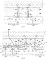
- Figure 1 illustrates a section of an IC as known in the art, including the power supply to an IC block 10, when the entire power delivery network is present on the backside of the IC, in accordance with EP3324436A1 .
- No header or footer transistors separate the block 10 from the power supply.
- the drawing makes abstraction of a number of well-known concepts, and shows only technical details which are essential for the context of the present invention.
- the IC comprises a silicon substrate 1 which may have a thickness in the order of 0.5 to 1 micrometre. For the sake of explaining the invention, the substrate is defined as a p-doped substrate.
- the substrate comprises a front end of line (FEOL) portion 1a and a bulk Si portion 1b.
- the FEOL portion 1a comprises a high number of active devices, such as CMOS transistors, processed according to any technology known in the art, such as finFET or the like. None of these devices are shown in detail.
- On top of the FEOL portion 1a is the back end of line portion (BEOL) 4, not shown in detail but well-known to the skilled reader.
- the BEOL comprises multiple interconnect levels for realizing circuit interconnects between the active devices in the FEOL.
- the interconnect levels comprise interconnect vias and conductors embedded in a dielectric material.
- the FEOL portion 1a further comprises multiple buried power rails 3a, 3b formed of a conductive material, usually a metal such as copper.
- the function and production method for obtaining the buried rails are described in EP3324436A1 .
- the buried rails connect the active devices of the FEOL portion 1a to the back of the substrate, through TSV connections 5a,5b which are preferably metal connections, isolated from the silicon by a liner 6 which may be formed of silicon oxide. Only two rails 3a,3b and two TSVs 5a,5b are shown.
- multiple rails are produced at regular intervals, alternately Vss-coupled and Vdd-coupled, while multiple TSVs are arranged for connecting the rails to the power delivery network 7 at the back of the substrate 1.
- Some of the buried rails may also be isolated by a liner (not shown) from the surrounding semiconductor material, depending on the layout of the FEOL portion 1a.
- the TSVs 5a and 5b need not necessarily be located in the same vertical plane, but for the sake of explaining the invention, they are drawn in this way.
- the TSVs are arranged in a pattern in which there is a shift between the position of the TSVs contacting two adjacent rails, as described in EP3324436A1 .
- the PDN 7 is an interconnect structure similar to the BEOL portion 4, through which the buried rails 3a,3b are coupled to a supply voltage terminal (Vdd) or a reference terminal (Vss) which are accessible at the back of the IC.
- Interconnect vias 7a,7b and conductors 8a,8b of the first PDN level are shown, which are connected respectively to the TSVs 5a and 5b. The remainder of the PDN is not shown in detail.
- Connections 9a,9b symbolize the further interconnect routing through the PDN from the respective conductors 8a,8b to the terminals Vss and Vdd.
- the IC block 10 comprises multiple interconnected active devices not shown in detail.
- Local interconnects 11a and 11b connect the block 10 respectively to the rails 3a and 3b.
- the voltage supply to the block 10 takes place through the first buried rail 3a and TSV 5a coupled to Vss and through the second buried rail 3b and TSV 5b coupled to Vdd.
- the block 10 is not necessarily coupled to Vss by a single TSV 5a, but it could be coupled to Vss through several TSVs, for example a row of TSVs perpendicular to the plane of the drawing, and all connected to the conductor 8a, which may extend in the direction perpendicular to the plane of the drawing. The same is true for the connection of the block 10 to Vdd.
- the IC block 10 in Figure 1 is not separated from the power supply by a header or footer transistor.
- the prior art solution to this would be to incorporate one or both of these transistors in the FEOL portion 1a.
- the header and/or the footer transistor is incorporated at the back of the substrate, as illustrated in Figure 2 , which shows the IC block 10 provided with a footer transistor, in accordance with an embodiment of the invention.
- the first level of the PDN 7 is partially buried in the substrate, at its backside, and one buried conductor is processed so as to serve as the gate electrode of the backside footer transistor 100 according to the invention.
- doped regions are provided on either side of the gate electrode, for creating the source and drain of the transistor, and a well or optionally threshold voltage shifting implant is provided above the gate electrode and separated therefrom by a gate dielectric.
- metal conductors 8a and 8b of the first PDN level are now buried in the substrate and uniform with the respective TSVs 5a and 5b. These conductors 8a and 8b are isolated from the substrate by lateral oxide layers 12a and 12b, and further by thin horizontal oxide layers 13a and 13b.
- the gate electrode 15 of the footer transistor is a metal contact pad equally buried in the substrate 1 at its backside. N-doped regions 16 and 17 are present on either side of the gate electrode 15, and separated from the gate by an oxide 18. The n-doped regions 16 and 17 are the source and drain regions of the footer transistor.
- Extending from the source to the drain is a p-doped region 19 having a higher dopant density than the substrate 1 and separated from the gate 15 by a thin oxide layer 20 which functions as the gate oxide of the transistor, and which is thinner than the oxide 18 separating the gate 15 from the source and drain regions 16 and 17.
- the region 19 having a higher dopant density is optional and may be implemented for shifting the threshold voltage of the transistor.
- charge carriers move in a channel region 23 between the source and drain regions 16 and 17 and immediately adjacent the gate electrode 20.
- the p-doped region 19 is not included, the source and drain regions 16 and 17 could extend further down into the substrate, beyond the gate electrode 15.
- the gate electrode 15 and the conductors 8a and 8b preferably have the same thickness.
- the oxide layers 12a, 12b and 13a, 13b preferably have the same thickness as the respective layers 18 and 20.
- Source and drain electrodes 21 and 22, preferably formed of a metal silicide, are provided on the source and drain regions 16 and 17 at the back surface of the substrate 1.
- the source electrode 21 of the footer is coupled to Vss through a via 25 and a conductor 26 of the PDN and through one or more further connections of the PDN symbolized by the line 27.
- the drain electrode 22 of the footer is coupled to the IC block 10 through vias 30 and conductor 31 of the PDN, which connect the drain electrode 22 to the conductor 8a.
- the TSV or TSVs 5a are thus no longer directly coupled to Vss. Instead, they are coupled to Vss via the footer transistor 100.
- the other buried rail 3b and TSV 5b are coupled to Vdd through a via 32 and a conductor 33 of the PDN and through one or more further connections of the PDN symbolized by the line 34.
- the gate electrode 15 is connected to a dedicated gate control terminal 35 at the back of the IC, through vias and conductors of the PDN, symbolized by reference numerals 36, 37 and 38. Through the gate control terminal 35, the footer transistor 100 can be switched on or off, thereby coupling or decoupling the IC block 10 to or from the power supply.
- Figure 3 shows an embodiment wherein a p-type header transistor 101 is incorporated at the back of the IC, between the IC block 10 and the Vdd terminal at the back, in an analogue way as the footer shown in Figure 2 .
- the various components are indicated with the same reference numerals, and the operation of the header transistor 101 is the same as the footer transistor of Figure 2 .
- the transistor is a p-type transistor
- an n-well 14 is provided at the back of the substrate 1
- the source and drain regions 16 and 17 are p-doped regions.
- a channel region 23 equivalent to the channel region in Figure 2 is now defined as a portion of the n-well 14 immediately adjacent the gate oxide 20.
- the source and drain regions 16 and 17 could extend further down into the substrate, beyond the gate electrode 15.
- Figure 4 shows an embodiment comprising both a footer transistor 100 and a header transistor 101.
- the transistor could be a depletion mode transistor instead of enhancement mode.
- An n-type depletion mode transistor may for example be obtained by implanting the area 19 in figure 2 with n-type dopants instead of p-type.
- Figures 2 to 4 show only two rails 3a and 3b, but in a standard design, there is a plurality of alternately Vss -and Vdd-coupled, regularly spaced rails.
- the transistor is integrated at the back side, taking into account the spacing between the rails and TSVs.
- Such an embodiment is illustrated in Figure 5 for the case of the footer transistor 100.
- the rails 3a and 3b are part of an array of regularly spaced rails, comprising further a Vdd coupled rail 3c and a Vss coupled rail 3d, the latter being connected through one or more TSVs 5d to a conductor 8d of the first PDN level, isolated from the substrate by oxide layers 12d and 13d.
- the Vdd coupled rail 3c is connected to one or more TSVs and conductors (not shown) outside the plane of the drawing.
- the transistor is now integrated in the space between the Vss-coupled rails 3a and 3d.
- the source 16 may be coupled to the conductor 8d through vias 40 and conductor 41 of the PDN.
- the header transistor 101 of Figure 3 may be integrated in a regular array of buried rails in an analogue way.
- the invention is not limited to the above-described embodiment wherein the conductors 8a, 8b, 8c and 8d of the first level of the PDN are buried in the substrate 1. Possibly, only the gate electrode 15 is buried in the substrate, and the first level of the PDN is produced in accordance with the prior art, i.e. on the back surface of the substrate 1.
- This embodiment is illustrated in Figure 6 , for the case of the footer transistor 100.
- the first level of the PDN 7 is now formed by the vias 25,36,30,7a and 7b and the conductors 26, 37, 8a and 8b.
- the gate 15 is produced on top of the back surface of the substrate 1. In this case, the gate oxide is an oxide layer 20 on top of the substrate 1.
- the gate electrode 15 is now embedded in the dielectric of the PDN 7, which is connected to the gate 15, and to the source and drain regions 16 and 17 in the same way as in the previous embodiment.
- the invention is not limited to the use of the transistor integrated at the back of the substrate as a header or footer transistor, i.e. a transistor for allowing or interrupting the power supply to an IC block 10.
- the transistor according to the invention could be implemented for example as part of a low drop-out (LDO) voltage converter, a charge pump circuit or high-voltage I/O transistor.
- LDO low drop-out
- I/O high-voltage I/O transistor.
- Two transistors according to the invention could be used as the pull-up and pull-down transistors of a buck converter circuit integrated in the IC.
- the invention is not limited to an IC comprising buried power rails 3a to 3d. Without the buried power rails, it is possible and known in the art to produce at least the voltage supply terminal and the reference terminal on the backside of the substrate, while at least one level of the PDN is on the front side, between the FEOL and the BEOL. TSV connections through the substrate then connect the terminals to the PDN.
- a field effect transistor in accordance with the invention may be integrated on the substrate's backside in the same way as described above, and connected to the Vss and Vdd terminals through conductors of the PDN located at the back side of the substrate.
- a method for producing the IC shown in Figure 2 is described hereafter, with reference to Figures 8a to 8p .
- a silicon process wafer 50 is provided and a thin etch stop layer 51, for example a SiGe layer is produced on its surface by epitaxial growth.
- a monocrystalline silicon layer 52 is produced on the SiGe layer 51, see Figure 8b .
- the SiGe layer 51 may have a thickness of a few tens of nanometres.
- the epitaxial Si-layer 52 may have a thickness of about 100nm.
- the Si-layer 52 may be subjected to a doping step (not shown) by implanting the complete layer with p-type doping elements, to turn the layer into a lightly p-doped layer. More preferably, the p-type doping is applied in situ during the epitaxial growth.
- a doping step (not shown) by implanting the complete layer with p-type doping elements, to turn the layer into a lightly p-doped layer. More preferably, the p-type doping is applied in situ during the epitaxial growth.
- an SOI (silicon on insulator) wafer could be taken as the starting point for the method.
- the insulator layer plays the part of the etch stop layer 51, the silicon layer on the insulator plays the part of the epitaxial layer 52.
- An n-type dopant implant step is performed in two limited areas of the layer 52 (see Figure 8c ) by masking the wafer except in these limited areas, thereby creating two n-doped regions 16 and 17 which will become the source and drain areas shown in Figure 2 .
- a further local p-type dopant implant step may be performed, for creating the p-doped region 19 of Figure 2 , see Figure 8d .
- the dopant densities are in accordance with standard values for the creation of source/drain junctions of a MOS type field effect transistor, well-known to the skilled person.
- a first dopant activation anneal step may be performed at this point, to activate the dopant elements.
- Epitaxial growth of silicon is then continued, as illustrated in Figure 8e , until the silicon substrate 1 is obtained on the SiGe layer 51.
- the substrate 1 has a thickness that may be in the order of 500nm.
- P-type doping of the Si substrate 1 may be realized by in-situ doping during the epitaxy.
- the FEOL portion 1a comprises the IC block 10 and at least two buried power rails : a first rail 3a destined to be coupled to the reference voltage Vss and a second rail 3b destined to be coupled to the supply voltage Vdd.
- the rails are connected to the IC block 10 via the local interconnects 11a and 11b.
- the process wafer 50 is then flipped and mounted on an auxiliary substrate (not shown), after which the process wafer 50 is removed by grinding and/or chemical mechanical polishing, and finally by a wet or dry (plasma) etch process, stopped by the etch stop layer 51.
- the back side of the substrate 1 is exposed, as shown in Figure 8g .
- the previously formed n-doped regions 16 and 17 are now exposed.
- the back side of the substrate is then patterned by lithography and etching, as illustrated in Figure 8h , to create a plurality of openings, for producing the buried conductors of the first PDN level.
- Three openings 53, 54a and 54b are shown.
- the first opening 53 is situated between the n-doped regions 16 and 17 and extends down to the p-doped area 19.
- the sides of the opening 53 are directly adjacent to the n-doped regions 16 and 17 and the bottom of the opening is directly adjacent to the p-doped area 19.
- the position of the second opening 54a as seen in the plane of the substrate 1 is such that the second opening 54a fully overlaps the width of the buried rail 3a destined to be coupled to Vss.
- the third opening 54b overlaps the width of the buried rail 3b destined to be coupled to Vdd.
- the length of the first opening 53 i.e. its dimension perpendicular to the plane of the drawing) will determine the length of the gate of the transistor.
- the length of the second and third opening 54a and 54b may be longer than the length of the first opening.
- a layer 55 of silicon oxide is then deposited conformally on the back side of the substrate.
- the oxide layer 55 may be about 10 nm thick.
- the oxide layer 55 forms a liner on the sidewalls and the bottom of the openings 53, 54a and 54b.
- via openings 56a and 56b are then etched, see Figure 8j , for producing the TSV connections between the buried rails and the backside PDN.
- the via 56a is etched through the bottom of the opening 54a and down to the buried rail 3a destined to be coupled to Vss
- the via 56b is etched through the bottom of the opening 54b and down to the buried rail 3b destined to be coupled to Vdd.
- This is followed by the conformal deposition of a thin silicon oxide layer 6, which forms a liner on the sidewalls and the bottom of the vias, see Figure 8k .
- the oxide layer 6 increases the thickness of the previously deposited oxide layer 55.
- the liner 6 is then removed from the bottom of the TSV openings 56a and 56b by a suitable etch process known in the art, preferably a maskless plasma etch process that creates a protective polymer layer on the sidewalls so that the oxide on the sidewalls is maintained while removing the liner from the bottom, see Figure 8l .
- a suitable etch process known in the art, preferably a maskless plasma etch process that creates a protective polymer layer on the sidewalls so that the oxide on the sidewalls is maintained while removing the liner from the bottom, see Figure 8l .
- a suitable process of this type is described for example in patent document EP3035369 .
- the plasma etch process is continued until it thins the oxide layer 55 at the bottom of the openings 53,54a and 54b down to a thickness that is suitable for making the remaining oxide layer 20 function as the gate oxide of the transistor.
- the oxide 18, 12a and 12b on the sidewalls of the openings 53, 54a and 54b maintains its thickness.
- the openings 53, 54a and 54b and the vias 56a and 56b are filled with a conductive material 60 (see Figure 8m ), preferably a metal such as copper, preferably by electroplating, and the back surface is planarized ( Fig. 8n ), until the substrate 1 is exposed, with the conductors 15, 8a and 8b buried in the substrate and accessible at the back of the substrate.
- the electroplating step has furthermore created the TSV connections 5a and 5b.
- TSV 5a is uniform with the contact pad 8a and TSV 5b is uniform with contact pad 8b.
- the metal pads 8a and 8b may have a higher length than the gate 15, and may in that case be uniform with multiple TSVs colinear with the TSVs 5a and 5b.
- TSVs 5a and 5b are not necessarily located in the same vertical plane.
- silicidation of the surface of the exposed n-doped regions 16 and 17 is performed ( Fig. 8o ), to produce the source and drain electrodes 21 and 22.
- This may be done in a manner known as such in the art, wherein a silicide forming metal is first deposited on the entire surface, then patterned to leave the metal at least on the semiconductor material in the electrode areas 16 and 17, followed by silicidation through heating, and if necessary the removal of unreacted silicide forming metal.
- Suitable silicide forming metals are Ni, NiPt, Co or Ti.
- the backside PDN is produced by damascene-type techniques, creating multiple interconnect levels.
- the PDN 7 comprises contact vias 7b, 30, 36 and 25 and conductors 8b,31,37 and 26.
- the remaining levels of the PDN are produced, including the Vdd, Vss terminals and the gate control terminal 35.
- the lines 9b,38 and 27 symbolize the respective connections through these remaining levels, of the TSV 5b to the Vdd terminal, of the source electrode 21 to the Vss terminal, and of the gate electrode 15 to the gate control terminal 35.
- a preferred method for producing the p-type transistor of Figure 3 comprises the same method steps, except for the formation of the doped regions 16 and 17.
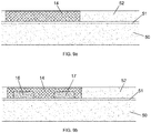
- an n-well 14 may first be created by implanting n-type dopant elements in the silicon layer 52, as illustrated in Figure 9a . This is followed by two deep p-type implants for forming the source and drain regions 16 and 17 ( Figure 9b ). Alternatively, the p-type implants 16 and 17 could be done prior to producing the n-well implant 14.
Landscapes
- Internal Circuitry In Semiconductor Integrated Circuit Devices (AREA)
- Metal-Oxide And Bipolar Metal-Oxide Semiconductor Integrated Circuits (AREA)
- Semiconductor Integrated Circuits (AREA)
Abstract
Description
- The present invention is related to semiconductor processing, in particular to the production of devices which are capable of operating as power switches for the supply of power to the logic devices on an integrated circuit chip.
- Some parts of an Integrated Circuit (IC) remain idle during long periods of time while the core is active, creating power dissipation due to static leakage, i.e. current leakage occurring when the transistors of the IC are not switching. One way to reduce the power consumption of the IC is to insert power gating transistors between well-defined blocks of the IC and the power delivery network (PDN) of the IC. Each block contains a number of active devices, such as CMOS transistors interconnected to form logic circuits. The power gating transistors are configured to cut off the power to an IC block when the block is not active, and to supply power to the block only when required. These power gating transistors are referred to as header or footer transistors. A header is coupled between a positive power supply voltage terminal of the network and the IC block. A footer transistor is coupled between a negative (or reference) terminal of the network and the IC block. The IC block may be separated from the power supply by a header, or a footer, or both. In presently known ICs, the header and/or footer transistors are incorporated in the front end of line portion of the IC, i.e. the portion that comprises the active devices of the IC.
- However, this solution presents drawbacks in terms of area and speed. The header and footer transistors need to be very large to have low resistance, since they are in series with the power rails of the PDN, hence representing a significant area consumption. If the ON resistance of the header/footer is not sufficiently low, the speed of the IC will be degraded. In addition, the header/footer transistors need to have a much smaller leakage (Ioff) than the logic block in order to reduce the static power of the IC. Therefore, the Ion/Ioff ratio of the header/footer must be significantly larger than the Ion/Ioff ratio of the logic block transistors, which is not easy to achieve when they are built in the front end of line.
- The invention aims to provide a solution to the above-described problems. This aim is achieved by an integrated circuit chip in accordance with the appended claims.
- The invention is related to an IC chip that includes a semiconductor substrate comprising active devices on its front side, and at least part of a power delivery network (PDN) on its back side. The PDN includes a power supply terminal and a reference terminal at the back of the IC. A plurality of TSV (Through Semiconductor Via) connections through the substrate bring the power to the front of the substrate. According to the invention, a field effect transistor is integrated at the back side of the substrate, and comprises a source electrode, a drain electrode and a gate electrode, which are contacted at said back side of the substrate. The IC further comprises a gate control terminal for controlling the gate voltage. The transistor is coupled between the power supply and one or more of the active devices of the IC. More specifically, one of the source and drain electrodes is connected to the power supply terminal or the reference terminal through conductors of the PDN at the back of the substrate, while the other is connected to one or more active devices through conductors of the PDN and through one or more TSVs. The backside transistor is particularly useful as a header or footer transistor that does not suffer from the above-described problems.
- At the back side of the chip, the area problem is not an issue. Moreover, a transistor produced in accordance with the invention can be activated by a power management IC (PMIC) which feeds the back-side of the chip. The high-voltage carried by the PMIC and the different process conditions of the back-side transistor enables higher Ion/Ioff ratios compared to header/footer transistors integrated in the front end of line.
- In particular, the invention is first related to an integrated circuit chip comprising :
- a semiconductor substrate, having a front side and a back side, the substrate comprising in a front portion of the substrate, a front end of line portion comprising a plurality of active devices
- a back end of line portion, on top of the FEOL portion,
- a power delivery network (PDN), the PDN including one or more interconnect levels, a power supply terminal and a reference terminal, at least the power supply terminal and the reference terminal being located at the back of the substrate,
- a plurality of Through Substrate Via (TSV) connections through the substrate, the TSVs being configured to enable the supply of power from the terminals at the back of the substrate to the active devices at the front of the substrate,
- the IC further comprises at least one field effect transistor at the back side of the substrate, the transistor comprising a source region and a drain region, both located in the substrate, and a gate electrode between the source and drain regions, wherein the source and drain regions and the gate electrode are contacted at the back of the substrate,
- The PDN further comprises a gate control terminal for controlling the gate voltage of the transistor,
- one of the source and drain regions is electrically connected to the power supply terminal or the reference terminal through one or more conductors of interconnect levels of the PDN, said conductors being located at the back side of the substrate, while the other terminal is electrically connected to one or more active devices through one or more conductors of the PDN and through one or more TSVs.
- According to an embodiment, the gate electrode is buried in the substrate at the back thereof and separated from the source and drain regions by a dielectric layer.
- In the latter embodiment, a plurality of conductors of the first PDN interconnect level may be buried in the substrate at the back thereof, wherein each of said plurality of conductors is uniform with one or more TSVs.
- According to an embodiment, the entire PDN is located at the back of the substrate, and wherein the FEOL portion comprises a plurality of buried rails, which connect the active devices to the TSVs, and wherein the buried rails may be connected through said TSVs and through the PDN, to the power supply terminal or to the reference terminal.
- According to an embodiment, the IC comprises an array of said buried rails which are alternately connected to the voltage supply terminal and to the reference terminal, and wherein the transistor is integrated in the space between two rails.
- According to an embodiment, the IC comprises a block of active devices coupled to the PDN through said TSVs, and wherein the field effect transistor is configured to act as a header or footer transistor for allowing or interrupting the supply of power to the IC block.
- According to an embodiment, the IC comprises both a header and a footer transistor for allowing or interrupting the supply of power to the IC block.
- The invention is furthermore related to a method for producing an integrated circuit chip in accordance with any one of the preceding claims, comprising the steps of :
- Providing a process wafer, comprising a first layer of semiconductor material on its surface,
- Implanting dopant elements into the first layer of semiconductor material, to form the source and drain regions of a field effect transistor, and if necessary, to form a well region into which the source and drain regions are embedded,
- depositing a further layer of the semiconductor material on the first layer, to obtain the substrate on the process wafer, consisting of the first layer, including the source and drain regions, and the further layer,
- Producing the FEOL portion in a front portion of the substrate, at the side opposite from the process wafer,
- Producing the BEOL portion on top of the FEOL portion,
- Removing the process wafer, to thereby expose the source and the drain regions at the back of the substrate,
- Etching openings from the back of the substrate and through the substrate for the TSV connections,
- Depositing a dielectric liner on the sidewalls and the bottom of the openings for the TSV connections,
- By a maskless etching process, removing the dielectric liner from the bottom of the TSV openings,
- Producing an electrically conductive layer on the substrate, filling the TSV openings to thereby form the TSVs,
- Planarizing the conductive layer,
- Producing the PDN or the remainder of the PDN, including the power supply and reference terminals,
- In the method as defined in the previous paragraph, the order in which the additional steps are performed relative to each other and to the other steps is not determined. The step of forming the gate electrode and gate dielectric may also be performed in a number of sub-steps, some of which may be done simultaneously with other steps of the method.
- According to an embodiment, the method further comprises the following steps, performed after exposing the source and drain regions at the back of the substrate and before etching the openings for the TSV connections:
- Etching an opening at the back of the substrate between the source and drain regions, two sidewalls of the opening being directly adjacent the source and drain regions, followed by :
- Depositing a dielectric layer conformally on the backside of the substrate,
- the maskless etching process thins the conformal dielectric layer on the bottom of the opening between the source and drain regions, so as to obtain a thin dielectric layer on the bottom of the opening, said layer being thinner than the dielectric layer that remains on the sidewalls of the opening,
- the electrically conductive layer fills the opening between the source and drain regions,
- the planarization of the conductive layer forms the gate electrode, separated from the substrate by the dielectric layer on the sidewalls of the opening and by the thin dielectric layer on the bottom of the opening, that thereby forms the gate dielectric of the transistor.
- According to an embodiment, the method further comprises the etching of additional openings at the back of the substrate, simultaneously with the etching of the opening between the source and drain regions, and :
- The TSV openings are etched through the bottom of the additional openings,
- The conformal dielectric layer and the liner are deposited also on the bottom and sidewalls of the additional openings,
- The maskless etching process results in a thin dielectric layer on the bottom of the additional openings while obtaining a thicker dielectric layer on the sidewalls of said additional openings,
- The conductive layer fills the TSV openings as well as the additional openings, thereby forming conductors of the first PDN level, which are buried in the substrate and which are uniform with one or more TSVs, the conductors being isolated from the substrate by the thin dielectric layers at the bottom of the additional openings and by the thicker dielectric layers on the sidewalls of the additional openings.
- According to an embodiment of the method, the FEOL portion comprises a plurality of buried rails, wherein the TSVs and the PDN may connect each of the rails to either the voltage supply terminal or the reference terminal.
-
-
Figure 1 illustrates a section of an integrated circuit chip as known in the art, wherein a block of active devices on the chip is supplied with power through a power delivery network arranged on the backside of the IC. -
Figure 2 illustrates the IC ofFigure 1 , further provided with a footer transistor in accordance with the invention, and wherein the conductors of the first level of the power delivery network (PDN) are buried in the semiconductor substrate. -
Figure 3 illustrates the IC ofFigure 1 , further provided with a header transistor in accordance with the invention, and wherein the conductors of the first level of the PDN are buried in the semiconductor substrate. -
Figure 4 illustrates the IC ofFigure 1 , provided with a footer and a header transistor in accordance with the invention. -
Figure 5 illustrates a footer transistor according to the invention, integrated in the space between two Vss-connected buried rails. -
Figure 6 illustrates an alternative design of the footer transistor of the invention, wherein only the gate electrode is buried in the substrate. -
Figure 7 illustrates another alternative embodiment of the invention, wherein the gate electrode is produced on top of the back surface of the substrate. -
Figures 8a to 8p illustrate key method steps of a method for producing the IC according toFigure 2 . -
Figures 9a and 9b show the steps for creating the n-well and p-type doped regions, as applicable in a method for producing the transistor ofFigure 3 . - A preferred embodiment of the invention takes advantage of a known development, which is the production of buried power rails integrated in the front end of line portion of the IC fabrication process. Reference is made to a previous patent application by the applicant, published as
EP3324436A1 , and incorporated herein by reference. In this patent application, buried power rails are connected by TSVs, to a power delivery network (PDN) that is located entirely on the backside of the chip. According to the preferred embodiment, one or more field effect transistors are integrated in this configuration, at the back of the semiconductor substrate that carries the active devices of the chip at its front, and the PDN at its back. The application of these transistors as a header or footer transistor will be described in detail hereafter. Based on this description, other uses will become apparent to the skilled person. - As a point of reference, with respect to which the invention will be described,
Figure 1 illustrates a section of an IC as known in the art, including the power supply to anIC block 10, when the entire power delivery network is present on the backside of the IC, in accordance withEP3324436A1 . No header or footer transistors separate theblock 10 from the power supply. The drawing makes abstraction of a number of well-known concepts, and shows only technical details which are essential for the context of the present invention. The IC comprises asilicon substrate 1 which may have a thickness in the order of 0.5 to 1 micrometre. For the sake of explaining the invention, the substrate is defined as a p-doped substrate. The substrate comprises a front end of line (FEOL)portion 1a and abulk Si portion 1b. TheFEOL portion 1a comprises a high number of active devices, such as CMOS transistors, processed according to any technology known in the art, such as finFET or the like. None of these devices are shown in detail. On top of theFEOL portion 1a is the back end of line portion (BEOL) 4, not shown in detail but well-known to the skilled reader. The BEOL comprises multiple interconnect levels for realizing circuit interconnects between the active devices in the FEOL. The interconnect levels comprise interconnect vias and conductors embedded in a dielectric material. - The
FEOL portion 1a further comprises multiple buriedpower rails EP3324436A1 . The buried rails connect the active devices of theFEOL portion 1a to the back of the substrate, throughTSV connections liner 6 which may be formed of silicon oxide. Only tworails TSVs EP3324436A1 , multiple rails are produced at regular intervals, alternately Vss-coupled and Vdd-coupled, while multiple TSVs are arranged for connecting the rails to thepower delivery network 7 at the back of thesubstrate 1. Some of the buried rails may also be isolated by a liner (not shown) from the surrounding semiconductor material, depending on the layout of theFEOL portion 1a. TheTSVs EP3324436A1 . - The
PDN 7 is an interconnect structure similar to theBEOL portion 4, through which the buriedrails Interconnect vias conductors TSVs Connections respective conductors - The
IC block 10 comprises multiple interconnected active devices not shown in detail.Local interconnects block 10 respectively to therails block 10 takes place through the first buriedrail 3a andTSV 5a coupled to Vss and through the second buriedrail 3b andTSV 5b coupled to Vdd. Theblock 10 is not necessarily coupled to Vss by asingle TSV 5a, but it could be coupled to Vss through several TSVs, for example a row of TSVs perpendicular to the plane of the drawing, and all connected to theconductor 8a, which may extend in the direction perpendicular to the plane of the drawing. The same is true for the connection of theblock 10 to Vdd. - As stated above, the
IC block 10 inFigure 1 is not separated from the power supply by a header or footer transistor. The prior art solution to this would be to incorporate one or both of these transistors in theFEOL portion 1a. According to the present invention, the header and/or the footer transistor is incorporated at the back of the substrate, as illustrated inFigure 2 , which shows theIC block 10 provided with a footer transistor, in accordance with an embodiment of the invention. - According to this embodiment, the first level of the
PDN 7 is partially buried in the substrate, at its backside, and one buried conductor is processed so as to serve as the gate electrode of thebackside footer transistor 100 according to the invention. In addition, doped regions are provided on either side of the gate electrode, for creating the source and drain of the transistor, and a well or optionally threshold voltage shifting implant is provided above the gate electrode and separated therefrom by a gate dielectric. - With reference to
Figure 2 ,metal conductors respective TSVs conductors lateral oxide layers horizontal oxide layers gate electrode 15 of the footer transistor is a metal contact pad equally buried in thesubstrate 1 at its backside. N-dopedregions gate electrode 15, and separated from the gate by anoxide 18. The n-dopedregions region 19 having a higher dopant density than thesubstrate 1 and separated from thegate 15 by athin oxide layer 20 which functions as the gate oxide of the transistor, and which is thinner than theoxide 18 separating thegate 15 from the source and drainregions region 19 having a higher dopant density is optional and may be implemented for shifting the threshold voltage of the transistor. When the transistor is in the ON state, charge carriers move in achannel region 23 between the source and drainregions gate electrode 20. When the p-dopedregion 19 is not included, the source and drainregions gate electrode 15. - As a consequence of a preferred production process applied for producing the footer transistor of
Figure 2 (see further), thegate electrode 15 and theconductors oxide layers respective layers - Source and
drain electrodes regions substrate 1. The source electrode 21 of the footer is coupled to Vss through a via 25 and aconductor 26 of the PDN and through one or more further connections of the PDN symbolized by theline 27. Thedrain electrode 22 of the footer is coupled to theIC block 10 throughvias 30 andconductor 31 of the PDN, which connect thedrain electrode 22 to theconductor 8a. The TSV orTSVs 5a are thus no longer directly coupled to Vss. Instead, they are coupled to Vss via thefooter transistor 100. - The other buried
rail 3b andTSV 5b are coupled to Vdd through a via 32 and aconductor 33 of the PDN and through one or more further connections of the PDN symbolized by theline 34. Thegate electrode 15 is connected to a dedicatedgate control terminal 35 at the back of the IC, through vias and conductors of the PDN, symbolized byreference numerals gate control terminal 35, thefooter transistor 100 can be switched on or off, thereby coupling or decoupling theIC block 10 to or from the power supply. -
Figure 3 shows an embodiment wherein a p-type header transistor 101 is incorporated at the back of the IC, between theIC block 10 and the Vdd terminal at the back, in an analogue way as the footer shown inFigure 2 . The various components are indicated with the same reference numerals, and the operation of theheader transistor 101 is the same as the footer transistor ofFigure 2 . As the transistor is a p-type transistor, an n-well 14 is provided at the back of thesubstrate 1, while the source and drainregions channel region 23 equivalent to the channel region inFigure 2 is now defined as a portion of the n-well 14 immediately adjacent thegate oxide 20. Here also, the source and drainregions gate electrode 15.Figure 4 shows an embodiment comprising both afooter transistor 100 and aheader transistor 101. - All of the header and footer transistors described above are enhancement mode transistors, but this is not a required limitation. The transistor could be a depletion mode transistor instead of enhancement mode. An n-type depletion mode transistor may for example be obtained by implanting the
area 19 infigure 2 with n-type dopants instead of p-type. -
Figures 2 to 4 show only tworails Figure 5 for the case of thefooter transistor 100. Therails rail 3c and a Vss coupledrail 3d, the latter being connected through one ormore TSVs 5d to a conductor 8d of the first PDN level, isolated from the substrate byoxide layers rail 3c is connected to one or more TSVs and conductors (not shown) outside the plane of the drawing. The transistor is now integrated in the space between the Vss-coupledrails source 16 may be coupled to the conductor 8d throughvias 40 andconductor 41 of the PDN. Theheader transistor 101 ofFigure 3 may be integrated in a regular array of buried rails in an analogue way. - The invention is not limited to the above-described embodiment wherein the
conductors substrate 1. Possibly, only thegate electrode 15 is buried in the substrate, and the first level of the PDN is produced in accordance with the prior art, i.e. on the back surface of thesubstrate 1. This embodiment is illustrated inFigure 6 , for the case of thefooter transistor 100. The first level of thePDN 7 is now formed by thevias conductors Figure 7 , thegate 15 is produced on top of the back surface of thesubstrate 1. In this case, the gate oxide is anoxide layer 20 on top of thesubstrate 1. Thegate electrode 15 is now embedded in the dielectric of thePDN 7, which is connected to thegate 15, and to the source and drainregions - The invention is not limited to the use of the transistor integrated at the back of the substrate as a header or footer transistor, i.e. a transistor for allowing or interrupting the power supply to an
IC block 10. The transistor according to the invention could be implemented for example as part of a low drop-out (LDO) voltage converter, a charge pump circuit or high-voltage I/O transistor. Two transistors according to the invention could be used as the pull-up and pull-down transistors of a buck converter circuit integrated in the IC. - Also, the invention is not limited to an IC comprising buried
power rails 3a to 3d. Without the buried power rails, it is possible and known in the art to produce at least the voltage supply terminal and the reference terminal on the backside of the substrate, while at least one level of the PDN is on the front side, between the FEOL and the BEOL. TSV connections through the substrate then connect the terminals to the PDN. In this case, a field effect transistor in accordance with the invention may be integrated on the substrate's backside in the same way as described above, and connected to the Vss and Vdd terminals through conductors of the PDN located at the back side of the substrate. - A method for producing the IC shown in
Figure 2 is described hereafter, with reference toFigures 8a to 8p . As seen inFigure 8a , asilicon process wafer 50 is provided and a thinetch stop layer 51, for example a SiGe layer is produced on its surface by epitaxial growth. Again by epitaxial growth, amonocrystalline silicon layer 52 is produced on theSiGe layer 51, seeFigure 8b . TheSiGe layer 51 may have a thickness of a few tens of nanometres. The epitaxial Si-layer 52 may have a thickness of about 100nm. The Si-layer 52 may be subjected to a doping step (not shown) by implanting the complete layer with p-type doping elements, to turn the layer into a lightly p-doped layer. More preferably, the p-type doping is applied in situ during the epitaxial growth. Instead of the above method steps, an SOI (silicon on insulator) wafer could be taken as the starting point for the method. The insulator layer plays the part of theetch stop layer 51, the silicon layer on the insulator plays the part of theepitaxial layer 52. - An n-type dopant implant step is performed in two limited areas of the layer 52 (see
Figure 8c ) by masking the wafer except in these limited areas, thereby creating two n-dopedregions Figure 2 . Optionally, a further local p-type dopant implant step may be performed, for creating the p-dopedregion 19 ofFigure 2 , seeFigure 8d . The dopant densities are in accordance with standard values for the creation of source/drain junctions of a MOS type field effect transistor, well-known to the skilled person. A first dopant activation anneal step may be performed at this point, to activate the dopant elements. Epitaxial growth of silicon is then continued, as illustrated inFigure 8e , until thesilicon substrate 1 is obtained on theSiGe layer 51. Thesubstrate 1 has a thickness that may be in the order of 500nm. P-type doping of theSi substrate 1 may be realized by in-situ doping during the epitaxy. - Known processing steps for producing the
FEOL portion 1a and theBEOL portion 4 of the chip are applied at the front surface, seeFigure 8f . TheFEOL portion 1a comprises theIC block 10 and at least two buried power rails : afirst rail 3a destined to be coupled to the reference voltage Vss and asecond rail 3b destined to be coupled to the supply voltage Vdd. The rails are connected to theIC block 10 via thelocal interconnects process wafer 50 is then flipped and mounted on an auxiliary substrate (not shown), after which theprocess wafer 50 is removed by grinding and/or chemical mechanical polishing, and finally by a wet or dry (plasma) etch process, stopped by theetch stop layer 51. Removal of the latter results in the back side of thesubstrate 1 being exposed, as shown inFigure 8g . The previously formed n-dopedregions Figure 8h , to create a plurality of openings, for producing the buried conductors of the first PDN level. Threeopenings first opening 53 is situated between the n-dopedregions area 19. The sides of theopening 53 are directly adjacent to the n-dopedregions area 19. The position of thesecond opening 54a as seen in the plane of thesubstrate 1 is such that thesecond opening 54a fully overlaps the width of the buriedrail 3a destined to be coupled to Vss. Thethird opening 54b overlaps the width of the buriedrail 3b destined to be coupled to Vdd. The length of the first opening 53 (i.e. its dimension perpendicular to the plane of the drawing) will determine the length of the gate of the transistor. The length of the second andthird opening - As shown in
Figure 8i , alayer 55 of silicon oxide is then deposited conformally on the back side of the substrate. Theoxide layer 55 may be about 10 nm thick. Theoxide layer 55 forms a liner on the sidewalls and the bottom of theopenings openings Figure 8j , for producing the TSV connections between the buried rails and the backside PDN. Only two vias relevant for the invention are shown : the via 56a is etched through the bottom of theopening 54a and down to the buriedrail 3a destined to be coupled to Vss, and the via 56b is etched through the bottom of theopening 54b and down to the buriedrail 3b destined to be coupled to Vdd. This is followed by the conformal deposition of a thinsilicon oxide layer 6, which forms a liner on the sidewalls and the bottom of the vias, seeFigure 8k . Theoxide layer 6 increases the thickness of the previously depositedoxide layer 55. Theliner 6 is then removed from the bottom of theTSV openings Figure 8l . A suitable process of this type is described for example in patent documentEP3035369 . The plasma etch process is continued until it thins theoxide layer 55 at the bottom of theopenings oxide layer 20 function as the gate oxide of the transistor. Like theliner 6 on the sidewalls of the vias, theoxide openings openings vias Figure 8m ), preferably a metal such as copper, preferably by electroplating, and the back surface is planarized (Fig. 8n ), until thesubstrate 1 is exposed, with theconductors TSV connections TSV 5a is uniform with thecontact pad 8a andTSV 5b is uniform withcontact pad 8b. Themetal pads gate 15, and may in that case be uniform with multiple TSVs colinear with theTSVs TSVs - After this, silicidation of the surface of the exposed n-doped
regions Fig. 8o ), to produce the source and drainelectrodes electrode areas - After this, the backside PDN is produced by damascene-type techniques, creating multiple interconnect levels. As seen in
Figure 8p , thePDN 7 comprisescontact vias conductors gate control terminal 35. Thelines TSV 5b to the Vdd terminal, of thesource electrode 21 to the Vss terminal, and of thegate electrode 15 to thegate control terminal 35. - A preferred method for producing the p-type transistor of
Figure 3 comprises the same method steps, except for the formation of the dopedregions silicon layer 52, as illustrated inFigure 9a . This is followed by two deep p-type implants for forming the source and drainregions 16 and 17 (Figure 9b ). Alternatively, the p-type implants well implant 14. - While the invention has been illustrated and described in detail in the drawings and foregoing description, such illustration and description are to be considered illustrative or exemplary and not restrictive. Other variations to the disclosed embodiments can be understood and effected by those skilled in the art in practicing the claimed invention, from a study of the drawings, the disclosure and the appended claims. In the claims, the word "comprising" does not exclude other elements or steps, and the indefinite article "a" or "an" does not exclude a plurality. The mere fact that certain measures are recited in mutually different dependent claims does not indicate that a combination of these measures cannot be used to advantage. Any reference signs in the claims should not be construed as limiting the scope.
Claims (11)
- An integrated circuit chip comprising :- a semiconductor substrate (1), having a front side and a back side, the substrate (1) comprising in a front portion of the substrate, a front end of line portion (1a) comprising a plurality of active devices- a back end of line portion (4), on top of the FEOL portion (1a),- a power delivery network (PDN)(7), the PDN including one or more interconnect levels, a power supply terminal (Vdd) and a reference terminal (Vss), at least the power supply terminal and the reference terminal being located at the back of the substrate (1),- a plurality of Through Substrate Via (TSV) connections (5a,5b) through the substrate (1), the TSVs being configured to enable the supply of power from the terminals (Vss,Vdd) at the back of the substrate to the active devices at the front of the substrate,characterized in that:- the IC further comprises at least one field effect transistor (100,101) at the back side of the substrate (1), the transistor comprising a source region (16) and a drain region (17), both located in the substrate (1), and a gate electrode (15) between the source and drain regions, wherein the source and drain regions (16,17) and the gate electrode (15) are contacted at the back of the substrate (1),- The PDN (7) further comprises a gate control terminal (35) for controlling the gate voltage of the transistor,- one of the source and drain regions (16,17) is electrically connected to the power supply terminal (Vdd) or the reference terminal (Vss) through one or more conductors of interconnect levels (25,26,27) of the PDN, said conductors being located at the back side of the substrate, while the other terminal is electrically connected to one or more active devices through one or more conductors (31,8a,8b) of the PDN and through one or more TSVs (5a,5b).
- The IC chip according to claim 1, wherein the gate electrode (15) is buried in the substrate (1) at the back thereof and separated from the source and drain regions (16,17) by a dielectric layer (18).
- The IC chip according to claim 2, wherein a plurality of conductors (8a,8b,8c,8d) of the first PDN interconnect level are buried in the substrate (1) at the back thereof, and wherein each of said plurality of conductors is uniform with one or more TSVs (5a,5b,5c,5d).
- The IC chip according to any one of the preceding claims, wherein the entire PDN (7) is located at the back of the substrate (1), and wherein the FEOL portion (1a) comprises a plurality of buried rails (3a,3b), which connect the active devices to the TSVs (5a,5b), and wherein the buried rails may be connected through said TSVs and through the PDN, to the power supply terminal (Vdd) or to the reference terminal (Vss).
- The IC chip according to claim 4, comprising an array of said buried rails (3a,3b,3c,3d) which are alternately connected to the voltage supply terminal (Vdd) and to the reference terminal (Vss), and wherein the transistor is integrated in the space between two rails.
- The IC chip according to any one of the preceding claims, wherein the IC comprises a block (10) of active devices coupled to the PDN (7) through said TSVs (5a,5b), and wherein the field effect transistor (100,101) is configured to act as a header or footer transistor for allowing or interrupting the supply of power to the IC block (10).
- The IC chip according to claim 6, comprising both a header and a footer transistor for allowing or interrupting the supply of power to the IC block (10).
- A method for producing an integrated circuit chip in accordance with any one of the preceding claims, comprising the steps of :- Providing a process wafer (50,51), comprising a first layer (52) of semiconductor material on its surface,- Implanting dopant elements into the first layer (52) of semiconductor material, to form the source (16) and drain (17) regions of a field effect transistor, and if necessary, to form a well region (14) into which the source and drain regions (16,17) are embedded,- depositing a further layer of the semiconductor material on the first layer (52), to obtain the substrate (1) on the process wafer, consisting of the first layer (52), including the source and drain regions (16,17), and the further layer,- Producing the FEOL portion (1a) in a front portion of the substrate (1), at the side opposite from the process wafer (50,51),- Producing the BEOL portion (4) on top of the FEOL portion (1a),- Removing the process wafer (50,51), to thereby expose the source (16) and the drain (17) regions at the back of the substrate (1),- Etching openings (56a,56b) from the back of the substrate and through the substrate (1) for the TSV connections,- Depositing a dielectric liner (6) on the sidewalls and the bottom of the openings (56a,56b) for the TSV connections,- By a maskless etching process, removing the dielectric liner (6) from the bottom of the TSV openings (56a,56b),- Producing an electrically conductive layer (60) on the substrate, filling the TSV openings (56a,56b) to thereby form the TSVs (5a,5b),- Planarizing the conductive layer (60),- Producing the PDN (7) or the remainder of the PDN (7), including the power supply and reference terminals (Vdd,Vss),the method further comprising the additional steps of forming source and drain electrodes (21,22) on the exposed source and drain regions (16,17) and of forming a gate electrode (15) and gate dielectric (20) at the back of the substrate (1).
- The method according to claim 8, further comprising the following steps, performed after exposing the source and drain regions (16,17) at the back of the substrate (1) and before etching the openings (56a,56b) for the TSV connections:- Etching an opening (53) at the back of the substrate between the source and drain regions (16,17), two sidewalls of the opening being directly adjacent the source and drain regions, followed by :- Depositing a dielectric layer (55) conformally on the backside of the substrate (1),and wherein the formation of the gate electrode (15) and gate dielectric (20) is realized as follows :- the maskless etching process thins the conformal dielectric layer (55) on the bottom of the opening (53) between the source and drain (16,17) regions, so as to obtain a thin dielectric layer (20) on the bottom of the opening (53), said layer being thinner than the dielectric layer (18) that remains on the sidewalls of the opening (53),- the electrically conductive layer (60) fills the opening (53) between the source and drain regions,- the planarization of the conductive layer (60), forms the gate electrode (15), separated from the substrate by the dielectric layer (18) on the sidewalls of the opening (53) and by the thin dielectric layer (20) on the bottom of the opening (53), that thereby forms the gate dielectric of the transistor.
- The method according to claim 9, further comprising the etching of additional openings (54a,54b) at the back of the substrate (1), simultaneously with the etching of the opening (53) between the source and drain regions (16,17), and wherein :- The TSV openings (56a,56b) are etched through the bottom of the additional openings (54a,54b),- The conformal dielectric layer (55) and the liner (6) are deposited also on the bottom and sidewalls of the additional openings (54a,54b),- The maskless etching process results in a thin dielectric layer (13a,13b) on the bottom of the additional openings (54a,54b) while obtaining a thicker dielectric layer (12a,12b) on the sidewalls of said additional openings,- The conductive layer (60) fills the TSV openings (56a,56b) as well as the additional openings (54a,54b), thereby forming conductors (8a,8b) of the first PDN level, which are buried in the substrate (1) and which are uniform with one or more TSVs (5a,5b), the conductors being isolated from the substrate (1) by the thin dielectric layers (13a,13b) at the bottom of the additional openings (54a,54b) and by the thicker dielectric layers (12a,12b) on the sidewalls of the additional openings.
- The method according to claim 9 or 10, wherein the FEOL portion (1a) comprises a plurality of buried rails (3a,3b), and wherein the TSVs (5a,5b) and the PDN (7) may connect each of the rails to either the voltage supply terminal (Vdd) or the reference terminal (Vss).
Priority Applications (2)
| Application Number | Priority Date | Filing Date | Title |
|---|---|---|---|
| EP19176249.1A EP3742487A1 (en) | 2019-05-23 | 2019-05-23 | An integrated circuit with backside power delivery network and backside transistor |
| US16/874,446 US11257764B2 (en) | 2019-05-23 | 2020-05-14 | Integrated circuit with backside power delivery network and backside transistor |
Applications Claiming Priority (1)
| Application Number | Priority Date | Filing Date | Title |
|---|---|---|---|
| EP19176249.1A EP3742487A1 (en) | 2019-05-23 | 2019-05-23 | An integrated circuit with backside power delivery network and backside transistor |
Publications (1)
| Publication Number | Publication Date |
|---|---|
| EP3742487A1 true EP3742487A1 (en) | 2020-11-25 |
Family
ID=66655149
Family Applications (1)
| Application Number | Title | Priority Date | Filing Date |
|---|---|---|---|
| EP19176249.1A Pending EP3742487A1 (en) | 2019-05-23 | 2019-05-23 | An integrated circuit with backside power delivery network and backside transistor |
Country Status (2)
| Country | Link |
|---|---|
| US (1) | US11257764B2 (en) |
| EP (1) | EP3742487A1 (en) |
Cited By (9)
| Publication number | Priority date | Publication date | Assignee | Title |
|---|---|---|---|---|
| KR20210086961A (en) * | 2019-12-30 | 2021-07-09 | 타이완 세미콘덕터 매뉴팩쳐링 컴퍼니 리미티드 | Header layout design including backside power rail |
| EP4123694A1 (en) * | 2021-07-22 | 2023-01-25 | Imec VZW | A semiconductor structure with an epitaxial layer stack for fabricating back-side contacts |
| WO2023038647A1 (en) * | 2021-09-09 | 2023-03-16 | Synopsys, Inc. | Power routing for 2.5d or 3d integrated circuits |
| EP4152381A1 (en) * | 2021-09-16 | 2023-03-22 | Imec VZW | An integrated circuit chip comprising back-side power delivery tracks |
| WO2023066797A1 (en) * | 2021-10-22 | 2023-04-27 | International Business Machines Corporation | Early backside first power delivery network |
| US11715501B2 (en) | 2019-12-30 | 2023-08-01 | Taiwan Semiconductor Manufacturing Company, Ltd. | Header layout design including backside power rail |
| WO2024068454A1 (en) * | 2022-09-30 | 2024-04-04 | International Business Machines Corporation | Power gating dummy power transistors for back side power delivery networks |
| TWI890036B (en) * | 2022-03-28 | 2025-07-11 | 南韓商三星電子股份有限公司 | Cmos structure |
| US12616019B2 (en) | 2022-06-10 | 2026-04-28 | International Business Machines Corporation | Via connection to backside power delivery network |
Families Citing this family (26)
| Publication number | Priority date | Publication date | Assignee | Title |
|---|---|---|---|---|
| US12444934B2 (en) * | 2020-03-31 | 2025-10-14 | Taiwan Semiconductor Manufacturing Company, Ltd. | Electrostatic discharge (ESD) protection circuit and method of operating the same |
| US11862561B2 (en) * | 2020-05-28 | 2024-01-02 | Taiwan Semiconductor Manufacturing Co., Ltd. | Semiconductor devices with backside routing and method of forming same |
| KR102821727B1 (en) | 2020-08-03 | 2025-06-19 | 삼성전자주식회사 | Semiconductor device and semiconductor package |
| US12255238B2 (en) * | 2020-10-27 | 2025-03-18 | Taiwan Semiconductor Manufacturing Company, Ltd. | Integrated circuit, system and method of forming same |
| KR102939312B1 (en) * | 2020-12-28 | 2026-03-12 | 삼성전자주식회사 | Integrated circuit devices |
| US12170277B2 (en) | 2021-02-09 | 2024-12-17 | Taiwan Semiconductor Manufacturing Company, Ltd. | Integrated circuit and manufacturing method of the same |
| US12237334B2 (en) * | 2021-07-16 | 2025-02-25 | Taiwan Semiconductor Manufacturing Company Ltd. | Semiconductor structure |
| US12136655B2 (en) | 2021-09-22 | 2024-11-05 | International Business Machines Corporation | Backside electrical contacts to buried power rails |
| US11990412B2 (en) | 2021-09-29 | 2024-05-21 | International Business Machines Corporation | Buried power rails located in a base layer including first, second, and third etch stop layers |
| KR102902644B1 (en) * | 2021-10-05 | 2025-12-23 | 삼성전자주식회사 | Semiconductor devices |
| CN116344450B (en) * | 2021-12-23 | 2026-04-24 | 中芯国际集成电路制造(上海)有限公司 | Semiconductor structure and its formation method |
| US12412836B2 (en) | 2022-05-11 | 2025-09-09 | International Business Machines Corporation | Backside power plane |
| US12550713B2 (en) * | 2022-06-30 | 2026-02-10 | International Business Machines Corporation | Hybrid buried power rail structure with dual front side and backside processing |
| EP4300561A1 (en) * | 2022-06-30 | 2024-01-03 | INTEL Corporation | Integrated circuit structures having vertical power gate transistor for backside power delivery |
| US12604674B2 (en) | 2022-08-23 | 2026-04-14 | International Business Machines Corporation | Back side phase change memory (PCM) with PCM back side source/drain contact structure |
| US12575402B2 (en) | 2022-09-16 | 2026-03-10 | International Business Machines Corporation | Non-planar metal-insulator-metal structure |
| US12453146B2 (en) | 2022-09-22 | 2025-10-21 | International Business Machines Corporation | Epi growth uniformity with source/drain placeholder |
| US12341099B2 (en) * | 2022-09-23 | 2025-06-24 | International Business Machines Corporation | Semiconductor backside transistor integration with backside power delivery network |
| US12575395B2 (en) | 2022-10-11 | 2026-03-10 | Samsung Electronics Co., Ltd. | Semiconductor device |
| US12550705B2 (en) | 2022-11-22 | 2026-02-10 | International Business Machines Corporation | Self-aligned backside gate contact |
| US12506049B2 (en) | 2022-12-05 | 2025-12-23 | International Business Machines Corporation | Transistors with backside source/drain contact and spacer |
| US20240202415A1 (en) * | 2022-12-20 | 2024-06-20 | Intel Corporation | High Density Transistor and Routing Track Architecture |
| US20240332184A1 (en) * | 2023-03-31 | 2024-10-03 | Adeia Semiconductor Bonding Technologies, Inc. | Direct bonding on buried power rails |
| US20250006837A1 (en) * | 2023-06-27 | 2025-01-02 | Intel Corporation | Integrated circuit structures having vertical-transport transistor with bottom source connection |
| US12581723B2 (en) | 2023-07-31 | 2026-03-17 | International Business Machines Corporation | Backside power via |
| US20250185292A1 (en) * | 2023-12-04 | 2025-06-05 | International Business Machines Corporation | Extra gate device integration with semiconductor device |
Citations (7)
| Publication number | Priority date | Publication date | Assignee | Title |
|---|---|---|---|---|
| WO2005104233A1 (en) * | 2004-04-27 | 2005-11-03 | Koninklijke Philips Electronics N.V. | Integrated circuit layout for virtual power supply |
| US20100224876A1 (en) * | 2009-03-05 | 2010-09-09 | International Business Machines Corporation | Two-Sided Semiconductor Structure |
| US20150187642A1 (en) * | 2013-12-30 | 2015-07-02 | International Business Machines Corporation | Double-sided segmented line architecture in 3d integration |
| US20160111369A1 (en) * | 2011-06-28 | 2016-04-21 | Monolithic 3D Inc. | Novel semiconductor system and device |
| EP3035369A1 (en) | 2014-12-18 | 2016-06-22 | IMEC vzw | Plasma treatment method |
| EP3324436A1 (en) | 2016-11-21 | 2018-05-23 | IMEC vzw | An integrated circuit chip with power delivery network on the backside of the chip |
| US20180277530A1 (en) * | 2015-03-09 | 2018-09-27 | Monolithic 3D Inc. | Methods for processing a 3d semiconductor device |
Family Cites Families (12)
| Publication number | Priority date | Publication date | Assignee | Title |
|---|---|---|---|---|
| KR101146972B1 (en) | 2005-03-16 | 2012-05-22 | 페어차일드코리아반도체 주식회사 | High voltage integrated circuit device having diode enduring high voltage |
| US7342287B2 (en) | 2005-07-19 | 2008-03-11 | International Business Machines Corporation | Power gating schemes in SOI circuits in hybrid SOI-epitaxial CMOS structures |
| US7714642B2 (en) | 2006-10-27 | 2010-05-11 | Texas Instruments Incorporated | Integrated virtual voltage circuit |
| US7485508B2 (en) * | 2007-01-26 | 2009-02-03 | International Business Machines Corporation | Two-sided semiconductor-on-insulator structures and methods of manufacturing the same |
| JP5258207B2 (en) * | 2007-05-29 | 2013-08-07 | セミコンダクター・コンポーネンツ・インダストリーズ・リミテッド・ライアビリティ・カンパニー | Semiconductor device |
| US8344496B1 (en) * | 2009-04-29 | 2013-01-01 | Altera Corporation | Distributing power with through-silicon-vias |
| KR101211044B1 (en) * | 2010-05-27 | 2012-12-12 | 에스케이하이닉스 주식회사 | Semiconductor integrated circuit having multi-chip structure |
| US8941180B2 (en) | 2011-03-10 | 2015-01-27 | International Business Machines Corporation | Integrated circuit structure incorporating one or more asymmetric field effect transistors as power gates for an electronic circuit with stacked symmetric field effect transistors |
| US8563403B1 (en) * | 2012-06-27 | 2013-10-22 | International Business Machines Corporation | Three dimensional integrated circuit integration using alignment via/dielectric bonding first and through via formation last |
| US9640531B1 (en) * | 2014-01-28 | 2017-05-02 | Monolithic 3D Inc. | Semiconductor device, structure and methods |
| US10950581B2 (en) * | 2014-01-28 | 2021-03-16 | Monolithic 3D Inc. | 3D semiconductor device and structure |
| US10475692B2 (en) | 2017-04-07 | 2019-11-12 | Globalfoundries Inc. | Self aligned buried power rail |
-
2019
- 2019-05-23 EP EP19176249.1A patent/EP3742487A1/en active Pending
-
2020
- 2020-05-14 US US16/874,446 patent/US11257764B2/en active Active
Patent Citations (7)
| Publication number | Priority date | Publication date | Assignee | Title |
|---|---|---|---|---|
| WO2005104233A1 (en) * | 2004-04-27 | 2005-11-03 | Koninklijke Philips Electronics N.V. | Integrated circuit layout for virtual power supply |
| US20100224876A1 (en) * | 2009-03-05 | 2010-09-09 | International Business Machines Corporation | Two-Sided Semiconductor Structure |
| US20160111369A1 (en) * | 2011-06-28 | 2016-04-21 | Monolithic 3D Inc. | Novel semiconductor system and device |
| US20150187642A1 (en) * | 2013-12-30 | 2015-07-02 | International Business Machines Corporation | Double-sided segmented line architecture in 3d integration |
| EP3035369A1 (en) | 2014-12-18 | 2016-06-22 | IMEC vzw | Plasma treatment method |
| US20180277530A1 (en) * | 2015-03-09 | 2018-09-27 | Monolithic 3D Inc. | Methods for processing a 3d semiconductor device |
| EP3324436A1 (en) | 2016-11-21 | 2018-05-23 | IMEC vzw | An integrated circuit chip with power delivery network on the backside of the chip |
Cited By (14)
| Publication number | Priority date | Publication date | Assignee | Title |
|---|---|---|---|---|
| US11715501B2 (en) | 2019-12-30 | 2023-08-01 | Taiwan Semiconductor Manufacturing Company, Ltd. | Header layout design including backside power rail |
| US12136466B2 (en) | 2019-12-30 | 2024-11-05 | Taiwan Semiconductor Manufacturing Company, Ltd. | Header layout design including backside power rail |
| KR20210086961A (en) * | 2019-12-30 | 2021-07-09 | 타이완 세미콘덕터 매뉴팩쳐링 컴퍼니 리미티드 | Header layout design including backside power rail |
| EP4123694A1 (en) * | 2021-07-22 | 2023-01-25 | Imec VZW | A semiconductor structure with an epitaxial layer stack for fabricating back-side contacts |
| WO2023038647A1 (en) * | 2021-09-09 | 2023-03-16 | Synopsys, Inc. | Power routing for 2.5d or 3d integrated circuits |
| US12581933B2 (en) | 2021-09-09 | 2026-03-17 | Synopsys, Inc. | Power routing for 2.5D or 3D integrated circuits including a buried power rail and interposer with power delivery network |
| US11984384B2 (en) | 2021-09-09 | 2024-05-14 | Synopsys, Inc. | Power routing for 2.5D or 3D integrated circuits including a buried power rail and interposer with power delivery network |
| US12557634B2 (en) | 2021-09-16 | 2026-02-17 | Imec Vzw | Integrated circuit chip including back side power delivery tracks |
| EP4152381A1 (en) * | 2021-09-16 | 2023-03-22 | Imec VZW | An integrated circuit chip comprising back-side power delivery tracks |
| WO2023066797A1 (en) * | 2021-10-22 | 2023-04-27 | International Business Machines Corporation | Early backside first power delivery network |
| US12482746B2 (en) | 2021-10-22 | 2025-11-25 | International Business Machines Corporation | Early backside first power delivery network |
| TWI890036B (en) * | 2022-03-28 | 2025-07-11 | 南韓商三星電子股份有限公司 | Cmos structure |
| US12616019B2 (en) | 2022-06-10 | 2026-04-28 | International Business Machines Corporation | Via connection to backside power delivery network |
| WO2024068454A1 (en) * | 2022-09-30 | 2024-04-04 | International Business Machines Corporation | Power gating dummy power transistors for back side power delivery networks |
Also Published As
| Publication number | Publication date |
|---|---|
| US11257764B2 (en) | 2022-02-22 |
| US20200373242A1 (en) | 2020-11-26 |
Similar Documents
| Publication | Publication Date | Title |
|---|---|---|
| US11257764B2 (en) | Integrated circuit with backside power delivery network and backside transistor | |
| US11121086B2 (en) | Vertical isolated gate field effect transistor integrated in a semiconductor chip | |
| US11862561B2 (en) | Semiconductor devices with backside routing and method of forming same | |
| US11664374B2 (en) | Backside interconnect structures for semiconductor devices and methods of forming the same | |
| US12159869B2 (en) | Backside interconnect structures for semiconductor devices and methods of forming the same | |
| US6495454B2 (en) | Substrate interconnect for power distribution on integrated circuits | |
| US10916468B2 (en) | Semiconductor device with buried local interconnects | |
| KR102655099B1 (en) | Transistor structure and related inverter | |
| US20240096805A1 (en) | Semiconductor devices with backside routing and method of forming same | |
| US20240203994A1 (en) | Integrated Circuit Device and a Method for Forming the Same | |
| US8766360B2 (en) | Insulative cap for borderless self-aligning contact in semiconductor device | |
| US7575958B2 (en) | Programmable fuse with silicon germanium | |
| US20240420960A1 (en) | Inverted gate cut region | |
| US6441456B1 (en) | Semiconductor device and a process for manufacturing the same | |
| US6958275B2 (en) | MOSFET power transistors and methods | |
| US10079248B2 (en) | Field-effect transistors with a buried body contact | |
| WO2025151200A1 (en) | Sidewall metal contact integration through the direct etch of a merged source-and-drain contact | |
| US20250098288A1 (en) | Backside resistor connected to backside back end of line network | |
| US20240363617A1 (en) | Electrostatic discharge using backside power distribution network | |
| US10304839B2 (en) | Metal strap for DRAM/FinFET combination | |
| EP4152381B1 (en) | An integrated circuit chip comprising back-side power delivery tracks | |
| JP2002064206A (en) | Semiconductor device and manufacturing method thereof | |
| US6905924B2 (en) | Diode structure for SOI circuits | |
| US20250311256A1 (en) | Semiconductor device | |
| EP4287246A1 (en) | A method for producing an interconnect rail for contacting a semiconductor device from the back side |
Legal Events
| Date | Code | Title | Description |
|---|---|---|---|
| PUAI | Public reference made under article 153(3) epc to a published international application that has entered the european phase |
Free format text: ORIGINAL CODE: 0009012 |
|
| STAA | Information on the status of an ep patent application or granted ep patent |
Free format text: STATUS: THE APPLICATION HAS BEEN PUBLISHED |
|
| AK | Designated contracting states |
Kind code of ref document: A1 Designated state(s): AL AT BE BG CH CY CZ DE DK EE ES FI FR GB GR HR HU IE IS IT LI LT LU LV MC MK MT NL NO PL PT RO RS SE SI SK SM TR |
|
| AX | Request for extension of the european patent |
Extension state: BA ME |
|
| STAA | Information on the status of an ep patent application or granted ep patent |
Free format text: STATUS: REQUEST FOR EXAMINATION WAS MADE |
|
| 17P | Request for examination filed |
Effective date: 20210518 |
|
| RBV | Designated contracting states (corrected) |
Designated state(s): AL AT BE BG CH CY CZ DE DK EE ES FI FR GB GR HR HU IE IS IT LI LT LU LV MC MK MT NL NO PL PT RO RS SE SI SK SM TR |
|
| STAA | Information on the status of an ep patent application or granted ep patent |
Free format text: STATUS: EXAMINATION IS IN PROGRESS |
|
| 17Q | First examination report despatched |
Effective date: 20220317 |