EP3739756A1 - Cascode semiconductor device and method of manufacture - Google Patents
Cascode semiconductor device and method of manufacture Download PDFInfo
- Publication number
- EP3739756A1 EP3739756A1 EP19175165.0A EP19175165A EP3739756A1 EP 3739756 A1 EP3739756 A1 EP 3739756A1 EP 19175165 A EP19175165 A EP 19175165A EP 3739756 A1 EP3739756 A1 EP 3739756A1
- Authority
- EP
- European Patent Office
- Prior art keywords
- high voltage
- gate
- connection
- drain
- low voltage
- Prior art date
- Legal status (The legal status is an assumption and is not a legal conclusion. Google has not performed a legal analysis and makes no representation as to the accuracy of the status listed.)
- Withdrawn
Links
Images



Classifications
-
- H—ELECTRICITY
- H10—SEMICONDUCTOR DEVICES; ELECTRIC SOLID-STATE DEVICES NOT OTHERWISE PROVIDED FOR
- H10W—GENERIC PACKAGES, INTERCONNECTIONS, CONNECTORS OR OTHER CONSTRUCTIONAL DETAILS OF DEVICES COVERED BY CLASS H10
- H10W40/00—Arrangements for thermal protection or thermal control
- H10W40/20—Arrangements for cooling
- H10W40/25—Arrangements for cooling characterised by their materials
- H10W40/255—Arrangements for cooling characterised by their materials having a laminate or multilayered structure, e.g. direct bond copper [DBC] ceramic substrates
-
- H—ELECTRICITY
- H10—SEMICONDUCTOR DEVICES; ELECTRIC SOLID-STATE DEVICES NOT OTHERWISE PROVIDED FOR
- H10W—GENERIC PACKAGES, INTERCONNECTIONS, CONNECTORS OR OTHER CONSTRUCTIONAL DETAILS OF DEVICES COVERED BY CLASS H10
- H10W70/00—Package substrates; Interposers; Redistribution layers [RDL]
- H10W70/60—Insulating or insulated package substrates; Interposers; Redistribution layers
- H10W70/611—Insulating or insulated package substrates; Interposers; Redistribution layers for connecting multiple chips together
-
- H—ELECTRICITY
- H03—ELECTRONIC CIRCUITRY
- H03K—PULSE TECHNIQUE
- H03K17/00—Electronic switching or gating, i.e. not by contact-making and –breaking
- H03K17/10—Modifications for increasing the maximum permissible switched voltage
- H03K17/102—Modifications for increasing the maximum permissible switched voltage in field-effect transistor switches
-
- H—ELECTRICITY
- H10—SEMICONDUCTOR DEVICES; ELECTRIC SOLID-STATE DEVICES NOT OTHERWISE PROVIDED FOR
- H10W—GENERIC PACKAGES, INTERCONNECTIONS, CONNECTORS OR OTHER CONSTRUCTIONAL DETAILS OF DEVICES COVERED BY CLASS H10
- H10W70/00—Package substrates; Interposers; Redistribution layers [RDL]
- H10W70/40—Leadframes
- H10W70/421—Shapes or dispositions
-
- H—ELECTRICITY
- H10—SEMICONDUCTOR DEVICES; ELECTRIC SOLID-STATE DEVICES NOT OTHERWISE PROVIDED FOR
- H10W—GENERIC PACKAGES, INTERCONNECTIONS, CONNECTORS OR OTHER CONSTRUCTIONAL DETAILS OF DEVICES COVERED BY CLASS H10
- H10W70/00—Package substrates; Interposers; Redistribution layers [RDL]
- H10W70/40—Leadframes
- H10W70/481—Leadframes for devices being provided for in groups H10D8/00 - H10D48/00
-
- H—ELECTRICITY
- H10—SEMICONDUCTOR DEVICES; ELECTRIC SOLID-STATE DEVICES NOT OTHERWISE PROVIDED FOR
- H10W—GENERIC PACKAGES, INTERCONNECTIONS, CONNECTORS OR OTHER CONSTRUCTIONAL DETAILS OF DEVICES COVERED BY CLASS H10
- H10W70/00—Package substrates; Interposers; Redistribution layers [RDL]
- H10W70/60—Insulating or insulated package substrates; Interposers; Redistribution layers
- H10W70/611—Insulating or insulated package substrates; Interposers; Redistribution layers for connecting multiple chips together
- H10W70/614—Insulating or insulated package substrates; Interposers; Redistribution layers for connecting multiple chips together the multiple chips being integrally enclosed
-
- H—ELECTRICITY
- H10—SEMICONDUCTOR DEVICES; ELECTRIC SOLID-STATE DEVICES NOT OTHERWISE PROVIDED FOR
- H10W—GENERIC PACKAGES, INTERCONNECTIONS, CONNECTORS OR OTHER CONSTRUCTIONAL DETAILS OF DEVICES COVERED BY CLASS H10
- H10W70/00—Package substrates; Interposers; Redistribution layers [RDL]
- H10W70/60—Insulating or insulated package substrates; Interposers; Redistribution layers
- H10W70/62—Insulating or insulated package substrates; Interposers; Redistribution layers characterised by their interconnections
- H10W70/65—Shapes or dispositions of interconnections
-
- H—ELECTRICITY
- H10—SEMICONDUCTOR DEVICES; ELECTRIC SOLID-STATE DEVICES NOT OTHERWISE PROVIDED FOR
- H10W—GENERIC PACKAGES, INTERCONNECTIONS, CONNECTORS OR OTHER CONSTRUCTIONAL DETAILS OF DEVICES COVERED BY CLASS H10
- H10W74/00—Encapsulations, e.g. protective coatings
- H10W74/10—Encapsulations, e.g. protective coatings characterised by their shape or disposition
- H10W74/111—Encapsulations, e.g. protective coatings characterised by their shape or disposition the semiconductor body being completely enclosed
- H10W74/114—Encapsulations, e.g. protective coatings characterised by their shape or disposition the semiconductor body being completely enclosed by a substrate and the encapsulations
-
- H—ELECTRICITY
- H10—SEMICONDUCTOR DEVICES; ELECTRIC SOLID-STATE DEVICES NOT OTHERWISE PROVIDED FOR
- H10W—GENERIC PACKAGES, INTERCONNECTIONS, CONNECTORS OR OTHER CONSTRUCTIONAL DETAILS OF DEVICES COVERED BY CLASS H10
- H10W90/00—Package configurations
-
- H—ELECTRICITY
- H10—SEMICONDUCTOR DEVICES; ELECTRIC SOLID-STATE DEVICES NOT OTHERWISE PROVIDED FOR
- H10W—GENERIC PACKAGES, INTERCONNECTIONS, CONNECTORS OR OTHER CONSTRUCTIONAL DETAILS OF DEVICES COVERED BY CLASS H10
- H10W90/00—Package configurations
- H10W90/20—Configurations of stacked chips
- H10W90/28—Configurations of stacked chips the stacked chips having different sizes, e.g. chip stacks having a pyramidal shape
-
- H—ELECTRICITY
- H10—SEMICONDUCTOR DEVICES; ELECTRIC SOLID-STATE DEVICES NOT OTHERWISE PROVIDED FOR
- H10W—GENERIC PACKAGES, INTERCONNECTIONS, CONNECTORS OR OTHER CONSTRUCTIONAL DETAILS OF DEVICES COVERED BY CLASS H10
- H10W90/00—Package configurations
- H10W90/811—Multiple chips on leadframes
-
- H—ELECTRICITY
- H03—ELECTRONIC CIRCUITRY
- H03K—PULSE TECHNIQUE
- H03K17/00—Electronic switching or gating, i.e. not by contact-making and –breaking
- H03K17/51—Electronic switching or gating, i.e. not by contact-making and –breaking characterised by the components used
- H03K17/56—Electronic switching or gating, i.e. not by contact-making and –breaking characterised by the components used by the use, as active elements, of semiconductor devices
- H03K17/687—Electronic switching or gating, i.e. not by contact-making and –breaking characterised by the components used by the use, as active elements, of semiconductor devices the devices being field-effect transistors
- H03K2017/6875—Electronic switching or gating, i.e. not by contact-making and –breaking characterised by the components used by the use, as active elements, of semiconductor devices the devices being field-effect transistors using self-conductive, depletion FETs
-
- H—ELECTRICITY
- H10—SEMICONDUCTOR DEVICES; ELECTRIC SOLID-STATE DEVICES NOT OTHERWISE PROVIDED FOR
- H10W—GENERIC PACKAGES, INTERCONNECTIONS, CONNECTORS OR OTHER CONSTRUCTIONAL DETAILS OF DEVICES COVERED BY CLASS H10
- H10W72/00—Interconnections or connectors in packages
- H10W72/071—Connecting or disconnecting
- H10W72/073—Connecting or disconnecting of die-attach connectors
- H10W72/07351—Connecting or disconnecting of die-attach connectors characterised by changes in properties of the die-attach connectors during connecting
- H10W72/07354—Connecting or disconnecting of die-attach connectors characterised by changes in properties of the die-attach connectors during connecting changes in dispositions
-
- H—ELECTRICITY
- H10—SEMICONDUCTOR DEVICES; ELECTRIC SOLID-STATE DEVICES NOT OTHERWISE PROVIDED FOR
- H10W—GENERIC PACKAGES, INTERCONNECTIONS, CONNECTORS OR OTHER CONSTRUCTIONAL DETAILS OF DEVICES COVERED BY CLASS H10
- H10W72/00—Interconnections or connectors in packages
- H10W72/071—Connecting or disconnecting
- H10W72/075—Connecting or disconnecting of bond wires
- H10W72/07551—Connecting or disconnecting of bond wires characterised by changes in properties of the bond wires during the connecting
- H10W72/07554—Connecting or disconnecting of bond wires characterised by changes in properties of the bond wires during the connecting changes in dispositions
-
- H—ELECTRICITY
- H10—SEMICONDUCTOR DEVICES; ELECTRIC SOLID-STATE DEVICES NOT OTHERWISE PROVIDED FOR
- H10W—GENERIC PACKAGES, INTERCONNECTIONS, CONNECTORS OR OTHER CONSTRUCTIONAL DETAILS OF DEVICES COVERED BY CLASS H10
- H10W72/00—Interconnections or connectors in packages
- H10W72/30—Die-attach connectors
- H10W72/341—Dispositions of die-attach connectors, e.g. layouts
- H10W72/347—Dispositions of multiple die-attach connectors
-
- H—ELECTRICITY
- H10—SEMICONDUCTOR DEVICES; ELECTRIC SOLID-STATE DEVICES NOT OTHERWISE PROVIDED FOR
- H10W—GENERIC PACKAGES, INTERCONNECTIONS, CONNECTORS OR OTHER CONSTRUCTIONAL DETAILS OF DEVICES COVERED BY CLASS H10
- H10W72/00—Interconnections or connectors in packages
- H10W72/30—Die-attach connectors
- H10W72/351—Materials of die-attach connectors
- H10W72/352—Materials of die-attach connectors comprising metals or metalloids, e.g. solders
-
- H—ELECTRICITY
- H10—SEMICONDUCTOR DEVICES; ELECTRIC SOLID-STATE DEVICES NOT OTHERWISE PROVIDED FOR
- H10W—GENERIC PACKAGES, INTERCONNECTIONS, CONNECTORS OR OTHER CONSTRUCTIONAL DETAILS OF DEVICES COVERED BY CLASS H10
- H10W72/00—Interconnections or connectors in packages
- H10W72/30—Die-attach connectors
- H10W72/351—Materials of die-attach connectors
- H10W72/353—Materials of die-attach connectors not comprising solid metals or solid metalloids, e.g. ceramics
- H10W72/354—Materials of die-attach connectors not comprising solid metals or solid metalloids, e.g. ceramics comprising polymers
-
- H—ELECTRICITY
- H10—SEMICONDUCTOR DEVICES; ELECTRIC SOLID-STATE DEVICES NOT OTHERWISE PROVIDED FOR
- H10W—GENERIC PACKAGES, INTERCONNECTIONS, CONNECTORS OR OTHER CONSTRUCTIONAL DETAILS OF DEVICES COVERED BY CLASS H10
- H10W72/00—Interconnections or connectors in packages
- H10W72/50—Bond wires
- H10W72/541—Dispositions of bond wires
- H10W72/547—Dispositions of multiple bond wires
-
- H—ELECTRICITY
- H10—SEMICONDUCTOR DEVICES; ELECTRIC SOLID-STATE DEVICES NOT OTHERWISE PROVIDED FOR
- H10W—GENERIC PACKAGES, INTERCONNECTIONS, CONNECTORS OR OTHER CONSTRUCTIONAL DETAILS OF DEVICES COVERED BY CLASS H10
- H10W72/00—Interconnections or connectors in packages
- H10W72/60—Strap connectors, e.g. thick copper clips for grounding of power devices
- H10W72/631—Shapes of strap connectors
- H10W72/634—Cross-sectional shape
-
- H—ELECTRICITY
- H10—SEMICONDUCTOR DEVICES; ELECTRIC SOLID-STATE DEVICES NOT OTHERWISE PROVIDED FOR
- H10W—GENERIC PACKAGES, INTERCONNECTIONS, CONNECTORS OR OTHER CONSTRUCTIONAL DETAILS OF DEVICES COVERED BY CLASS H10
- H10W72/00—Interconnections or connectors in packages
- H10W72/851—Dispositions of multiple connectors or interconnections
- H10W72/853—On the same surface
- H10W72/856—Bump connectors and die-attach connectors
-
- H—ELECTRICITY
- H10—SEMICONDUCTOR DEVICES; ELECTRIC SOLID-STATE DEVICES NOT OTHERWISE PROVIDED FOR
- H10W—GENERIC PACKAGES, INTERCONNECTIONS, CONNECTORS OR OTHER CONSTRUCTIONAL DETAILS OF DEVICES COVERED BY CLASS H10
- H10W72/00—Interconnections or connectors in packages
- H10W72/851—Dispositions of multiple connectors or interconnections
- H10W72/874—On different surfaces
- H10W72/877—Bump connectors and die-attach connectors
-
- H—ELECTRICITY
- H10—SEMICONDUCTOR DEVICES; ELECTRIC SOLID-STATE DEVICES NOT OTHERWISE PROVIDED FOR
- H10W—GENERIC PACKAGES, INTERCONNECTIONS, CONNECTORS OR OTHER CONSTRUCTIONAL DETAILS OF DEVICES COVERED BY CLASS H10
- H10W90/00—Package configurations
- H10W90/701—Package configurations characterised by the relative positions of pads or connectors relative to package parts
- H10W90/721—Package configurations characterised by the relative positions of pads or connectors relative to package parts of bump connectors
- H10W90/726—Package configurations characterised by the relative positions of pads or connectors relative to package parts of bump connectors between a chip and a stacked lead frame, conducting package substrate or heat sink
-
- H—ELECTRICITY
- H10—SEMICONDUCTOR DEVICES; ELECTRIC SOLID-STATE DEVICES NOT OTHERWISE PROVIDED FOR
- H10W—GENERIC PACKAGES, INTERCONNECTIONS, CONNECTORS OR OTHER CONSTRUCTIONAL DETAILS OF DEVICES COVERED BY CLASS H10
- H10W90/00—Package configurations
- H10W90/701—Package configurations characterised by the relative positions of pads or connectors relative to package parts
- H10W90/731—Package configurations characterised by the relative positions of pads or connectors relative to package parts of die-attach connectors
- H10W90/732—Package configurations characterised by the relative positions of pads or connectors relative to package parts of die-attach connectors between stacked chips
-
- H—ELECTRICITY
- H10—SEMICONDUCTOR DEVICES; ELECTRIC SOLID-STATE DEVICES NOT OTHERWISE PROVIDED FOR
- H10W—GENERIC PACKAGES, INTERCONNECTIONS, CONNECTORS OR OTHER CONSTRUCTIONAL DETAILS OF DEVICES COVERED BY CLASS H10
- H10W90/00—Package configurations
- H10W90/701—Package configurations characterised by the relative positions of pads or connectors relative to package parts
- H10W90/731—Package configurations characterised by the relative positions of pads or connectors relative to package parts of die-attach connectors
- H10W90/734—Package configurations characterised by the relative positions of pads or connectors relative to package parts of die-attach connectors between a chip and a stacked insulating package substrate, interposer or RDL
-
- H—ELECTRICITY
- H10—SEMICONDUCTOR DEVICES; ELECTRIC SOLID-STATE DEVICES NOT OTHERWISE PROVIDED FOR
- H10W—GENERIC PACKAGES, INTERCONNECTIONS, CONNECTORS OR OTHER CONSTRUCTIONAL DETAILS OF DEVICES COVERED BY CLASS H10
- H10W90/00—Package configurations
- H10W90/701—Package configurations characterised by the relative positions of pads or connectors relative to package parts
- H10W90/751—Package configurations characterised by the relative positions of pads or connectors relative to package parts of bond wires
- H10W90/754—Package configurations characterised by the relative positions of pads or connectors relative to package parts of bond wires between a chip and a stacked insulating package substrate, interposer or RDL
-
- H—ELECTRICITY
- H10—SEMICONDUCTOR DEVICES; ELECTRIC SOLID-STATE DEVICES NOT OTHERWISE PROVIDED FOR
- H10W—GENERIC PACKAGES, INTERCONNECTIONS, CONNECTORS OR OTHER CONSTRUCTIONAL DETAILS OF DEVICES COVERED BY CLASS H10
- H10W90/00—Package configurations
- H10W90/701—Package configurations characterised by the relative positions of pads or connectors relative to package parts
- H10W90/751—Package configurations characterised by the relative positions of pads or connectors relative to package parts of bond wires
- H10W90/755—Package configurations characterised by the relative positions of pads or connectors relative to package parts of bond wires between a chip and a laterally-adjacent insulating package substrate, interpose or RDL
-
- H—ELECTRICITY
- H10—SEMICONDUCTOR DEVICES; ELECTRIC SOLID-STATE DEVICES NOT OTHERWISE PROVIDED FOR
- H10W—GENERIC PACKAGES, INTERCONNECTIONS, CONNECTORS OR OTHER CONSTRUCTIONAL DETAILS OF DEVICES COVERED BY CLASS H10
- H10W90/00—Package configurations
- H10W90/701—Package configurations characterised by the relative positions of pads or connectors relative to package parts
- H10W90/751—Package configurations characterised by the relative positions of pads or connectors relative to package parts of bond wires
- H10W90/756—Package configurations characterised by the relative positions of pads or connectors relative to package parts of bond wires between a chip and a stacked lead frame, conducting package substrate or heat sink
Definitions
- the present disclosure relates to a cascode semiconductor device and associated method of manufacture.
- this disclosure relates to a cascode arrangement of a depletion mode transistor die with an enhancement mode transistor die, and an associated method of assembling such an arrangement.
- cascode arrangements of transistors are well known, in particular for controlling normally on (or depletion mode), at zero gate-source voltage, high voltage semiconductor devices.
- Single package cascode arrangements can be used in switched mode applications, especially in power supplies, where efficient energy switching is required.
- the cascode arrangement 100 may comprise a normally off (or enhancement mode) low voltage device 102 is placed in series with a high voltage depletion mode device 104, by the common connection of a gate of the high voltage device 104 to a source of the low voltage device 102, and a drain of the low voltage device 102 to the source of the high voltage device 104.
- the high voltage depletion mode device 104 can thus be switched off when the drain source voltage of the low voltage enhancement mode device 102 reaches the threshold voltage of the high voltage device 104.
- the addition of a low voltage device enhancement mode device 102 in a cascode arrangement with the high voltage depletion mode device 104 therefore allows the normally on high voltage device to operate as a normally off, or enhancement mode device.
- the high voltage depletion mode device 104 may be a Gallium Nitride (GaN) or Silicon Carbide (SiC) based JFET or HEMT
- the low voltage enhancement mode device 102 may be a silicon (Si) based MOSFET and both the high and low voltage device are integrated into a single semiconductor device package 100.
- both high and low voltage devices are integrated into a single semiconductor device package 100
- the low voltage device 102 is then mounted, or stacked, on the high voltage device 104.
- the insulating material 106 may be a ceramic material. Ceramic based insulators are preferred over glass or porcelain insulators because they are more robust at high operating temperatures. In addition ceramic is also compatible with copper deposition processes to form so-called direct bond plated copper (DBPC) substrates.
- DBPC direct bond plated copper
- the insulating material 106 may be soldered 108 to the die pad 110 and likewise the high voltage device 104 may be soldered to the die pad 110. Drain and source connections 112 may made to the high voltage 104 device using appropriate wire bonds.
- the carrier 110 may be electrically connected to the high voltage device 104 or the low voltage device 102 by way of electrical vias (not illustrated) through the insulating material 106 to the die pad 110.
- cascode device connections between the respective gate, source and drain of the high and low voltage devices 102, 104 are currently formed by wire bonds 114, 116 to achieve the cascode configuration of Figure 1b .
- wire bond connections suffer from the problem of DC power and switching losses due to the inductance effects in the wires during operation.
- Using wire-bonded connections can result in higher parasitic inductances and capacitances, which can result in so-called gate bounce.
- Gate bounce is a false turn on mechanism where during high frequency switching operation, the high voltage device is switched to an "on" state when it should be in an "off' state.
- device resistances such as R DSon may increase and wire connections can be subject to failure particularly at high voltage operation of the high voltage device.
- First and second cascode arrangements 100, 100' may be arranged in a half-bridge configuration as shown in the circuit diagram of Figure 1c .
- the drain of the second cascode 100' arrangement is connected to the source terminal, common with the gate of the high voltage device 104, of the low voltage device 102.
- aspects of the present disclosure involve the placement of a high voltage transistor die with respect to the low voltage transistor die in a cascode arrangement and the manner of the electrical connections therebetween.
- a discrete cascode semiconductor device comprising: a high voltage depletion mode device die having gate, source and drain terminals arranged on a first major surface thereof; a low voltage enhancement mode device die having a gate and a source terminals formed on a first major surface thereof and a drain terminal formed on a second major surface opposite the first major surface; wherein the drain terminal of the high voltage device die is mounted on a drain connection; the source terminal of the low voltage device die and the gate terminal of the high voltage device are mounted on a common source connection; and the drain terminal of the low voltage device die is mounted on the source terminal of the high voltage device.
- the gate terminal of the low voltage device die may be mounted on a gate connection.
- the drain connection, common source connection and gate connection may be clip bond lead connections.
- the clip bond lead connections may comprise a bend intermediate a first and a second end, such that the connections are formed as gull wing leads.
- the clip bond lead connections may comprise mechanical support for the high voltage depletion mode device die and the low voltage enhancement mode device die.
- a carrier may be mounted on a second major surface of the high voltage device, wherein the carrier comprises a insulating core arranged between two outer metal layers.
- a top surface of the carrier may be exposed through a top surface of a mould material.
- semiconductor device comprising first and second cascode semiconductor devices according to an embodiment, wherein the first and second cascode semiconductor devices are arranged in a half bridge configuration.
- a method of manufacturing discrete cascode semiconductor device comprising: providing a high voltage depletion mode device die having gate, source and drain terminals arranged on a first major surface thereof; providing a low voltage enhancement mode device die having a gate and a source terminals formed on a first major surface thereof and a drain terminal formed on a second major surface opposite the first major surface; mounting the drain terminal of the high voltage device die on a drain connection; mounting the source terminal of the low voltage device die the gate terminal of the high voltage device on a common source connection; and mounting the drain terminal of the low voltage device die on a gate connection.
- the method may further comprise mounting the drain terminal of the low voltage device die on a gate connection.
- the drain connection, common source connection and gate connection may be clip bond lead connections.
- the method may further comprise further comprise providing a bend intermediate a first and a second end of the clip bond lead connections such that the connections are formed as gull wing leads.
- the clip bond lead connections may comprise mechanical support for the high voltage depletion mode device die and the low voltage enhancement mode device die.
- the method may further comprise mounting a carrier on a second major surface of the high voltage device, wherein the carrier comprises a insulating core arranged between two outer metal layers.
- a top surface of the carrier may be exposed through a top surface of a mould material.
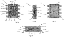
- Figures 2a to 2d illustrates various views of a discrete cascode semiconductor device 200 according to embodiments.
- the discrete cascode semiconductor device 200 comprises a high voltage depletion mode device 204 (hereinafter the high voltage device) and a low voltage enhancement mode device 202 (hereinafter the low voltage device).
- the high voltage device 204 and low voltage device 202 are separate device dies.
- the low voltage and high voltage devices 202, 204 are configured and integrated within a single package to form the semiconductor device 200 according to embodiments.
- the high voltage device 204 comprises gate 222, source 228 and drain 220 terminals on a first major surface thereof, and is thus considered to be a lateral device. This is as opposed to a vertical device where at least one of the terminals, typically the drain terminal, is formed on a second major surface, opposite the first surface.
- the low voltage device 202 comprises a gate 224 and source 226 terminals formed on a first major surface thereof and a drain terminal 218 formed on a second major surface thereof, and is thus considered to be a vertical device.
- each of the low and high voltage devices 202, 204 are configured and arranged for making electrical and mechanical connections thereto either by way of external leads of the semiconductor device 200 or low voltage to high voltage die connections, as discussed in more detail below.
- one or more gate terminals 222, the drain terminal 220 and the source terminal 228 are arranged on the first major surface thereof.
- Each of the gate 222, source 228 and drain 220 terminals are arranged so as to be co-planar on the first major surface, that is the gate, source and drain terminals 218, 222 and 220 are in the same plane on the first major surface.
- a drain connection 212 is electrically connected to and fixedly attached to the drain terminal 220.
- the drain connection 212 forms the external drain connection of the cascode semiconductor device 200.
- a source connection 214 is electrically connected to fixedly attached to the source terminal 226.
- the source connection 214 forms the external source connection or source lead of the cascode semiconductor device 200.
- the source connection 214 is electrically connected to and fixedly attached to the one or more gate terminals 222 of the high voltage device 204. This electrical connection of the one or more gate terminals 222 of the high voltage device 204 to the source terminal 226 of the low voltage device 202 forms with common high voltage device gate to low voltage device source connection consistent with the cascode circuit diagram discussed above with respect to Figure 1b .
- the source terminal 228 of the high voltage device 204 is electrically connected to and fixedly attached to the drain terminal 218 of the low voltage device 202.
- the drain terminal 218 of the low voltage device 202 is mounted on the source terminal 228 of the high voltage device 204 such that the low voltage device 202 is mounted and attached on the source terminal 228 of the high voltage device 204.
- the area of the source terminal 228 of the high voltage device 204 may be substantially equal or greater than the area of the drain terminal 218 of the low voltage device 202 to facilitate stacking of the low voltage device 202 on the source terminal 228 of the high voltage device 204.
- This electrical connection of the source terminal 228 of the high voltage device 204 to the drain terminal 218 form the common high voltage device source to low voltage drain connection consistent with the cascode circuit diagram discussed above with respect to Figure 1b .
- the drain of the cascode semiconductor device 200 is the drain of the high voltage device 204
- the gate of the cascode semiconductor device 200 is the gate of the low voltage device 202
- the source of the cascode semiconductor device 200 is common the high voltage device source to low voltage drain. This is consistent with the cascode circuit diagram discussed above with respect to Figure 1b .
- Figures 2a and 2d illustrate respective external gate, source and drain connections of the cascode device 200.
- the external drain of the cascode device 200 comprises the electrical and mechanical attachment of the external drain connection 212 to the drain terminal 220 of the high voltage device 204.
- the external gate of the cascode device 200 comprises the electrical and mechanical attachment of an external gate connection 216 to the gate terminal 224 of the low voltage device 202.
- the external source of the cascode device 200 comprises the electrical and mechanical attachment of the external source connection 214 to both the one or more gate terminals 222 of the high voltage device 204 and the source terminal 228 of the low voltage device 202. In this way the external source connection 214 provides the common connection of the one or more gate terminals 222 of the high voltage device 204 to the source terminal 228 of the low voltage device 202 consistent with the cascode circuit diagram discussed above with respect to Figure 1b .
- the external drain connection 212, external gate connection 216 and external source connection 214 of the cascode device 200 are each arranged as respective external leads.
- the respective gate, source and drain leads are each substantially elongate members, each having first and second distal ends.
- the respective first ends of the leads are configured and arranged for connection to contacts arranged on an external carrier such as a PCB (not illustrated).
- the leads may optionally comprise a bend 230 intermediate the first and the second end, such that the leads are formed as so-called "gull wing" leads.
- the respective second ends of the leads are configured and arranged to allow the respective terminals of the high voltage 204 and low voltage 202 devices, as set out above, to be electrically and mechanically attached thereto.
- the mechanical attachment of the external drain connection 212 to the drain terminal 220 of the high voltage device 204 provides a point of mechanical support to the high voltage device.
- the mechanical connection of the external source connection 214 to the one or more gate terminals 222 of the high voltage device provides one or more further points of mechanical support to the high voltage device.
- the mechanical support provided by both the external drain connection 212 and the source connection 214 is achieved by way of upstand portions 232, 234 arranged on the respective second ends thereof.
- the upstand portion 232 is dimensioned so as to substantially match the dimensions of the drain terminal 220 of the high voltage device 204.
- one or more upstand portions 234 are dimensioned so as to substantially match the dimensions of the respective one or more gate terminals of the high voltage device.
- the external source connection 214 also includes a downstand portion 236 to allow for electrical and mechanical connection of the source terminal 226 of the low voltage 202 to the external source connection 214, thus forming the common gate source connection between the high voltage and low voltage device.
- the arrangement of downstand also provides mechanical support for the low voltage device 202 mounted, via a common drain source connection, as discussed above, to the high voltage device 204. As illustrated in the side views of Figure 2b and Figure 2d the difference in high between contact surfaces, that is the respective surfaces of the upstand and downstand contacting the respective devices is substantially equal to the thickness of the low voltage device 202.
- the external gate connection 216 may also comprise a portion dimensioned so as to substantially match the dimensions of the gate terminal 224 of the low voltage device 204.
- the external drain connection 212 and the external source connection 214 may each be forked or branched to provide to provide a plurality of pin-outs.
- the current carrying capacity of external drain connection 212 and the external source connection 214 may be substantially equal.
- the above arrangement of the mechanical connection of the of the external connections to the respective terminals of the high and low voltage semiconductor devices allows for a cascode arrangement of high and low voltage devices 204, 202 that does not require a dedicated die pad or lead frame, let alone electrical connection of the high and low voltage devices to such a lead frame.
- the external connections act to support the high and low voltage devices of the cascode arrangement such that the cascode semiconductor device 200 according to embodiments can be considered free die pad or die pad-less.
- the present arrangement does not have a dedicated die pad and support for the high and low voltage devices 204, 202 is achieved using the mechanical connection of two or more leads to the high voltage device 204 and/or low voltage device.
- support for high voltage device 204 is provided by the source connection 214 and drain connection 212, and the support for the low voltage device 202 is provided by at least source connection 214.
- additional support may be provided for the high voltage device 204 and the low voltage device 202 by the gate connection 216.
- a second major surface of the high voltage device 204 may be fixedly attached by an adhesive layer 208 to a first major surface of an optional carrier 206.
- This adhesive layer 208 may be an insulating type adhesive since there is no electrical connection of the high voltage device 204 to the carrier 206.
- the carrier 206 may be a direct bond plated copper (DBPC) type carrier, comprising a three layer structure of an insulating ceramic core, such as AIN or Alumina, sandwiched between two outer copper layers.
- the copper layers may optionally be coated with a NiPd or an Ag metallisation layer to protect copper from oxidation.
- the carrier 206 acts as insulating layer between the high voltage device to the external connection and also increases the thermal performance.
- the top copper layer has allows for electrical connections thereto.
- a bottom copper layer, adjacent the high voltage device 204 is used to reduce the coefficient of thermal expansion mismatch between the high voltage device 204 and the core of the DBPC when the high voltage device is operating.
- a second major surface of the carrier 206 is arranged to be exposed through a top surface of a mould material 238 as illustrated in Figure 3a .
- the mould material 238 is arranged to encapsulate the high voltage 204 and low voltage 202 semiconductor devices and partially encapsulate the external gate, source and drain connections, by leaving the respective first ends of thereof free from mould material. This allows connection of the gate, source and drain connections to an external carrier such as the PCB.
- the low voltage device 202 is fixedly attached to the high voltage device 204, forming the common drain source connection discussed above by a further adhesive layer 209.
- the further adhesive layer may be a an electrically conductive layer, such as solder or conductive Ag sintering.
- Figures 4a to 4d illustrates a half bridge arrangement comprising first and second cascode devices 200, 200' of the type described above with respect to Figures 2a to 2d .
- the drain connection of the first cascode device 100 is extended to connect with the source connection of the second cascode device 100'.
- This connection may be achieved by way of common half bridge connection 240.
- the half bridge connection 240 provides the drain connection to the drain terminal of the high voltage device of the first cascode device 200 and the source connection to the source and gate terminals of the high voltage device of the second cascode device 200' consistent with the arrangement of Figures 2a to 2d .
- a carrier 206 acts as insulating layer between the high voltage device to the external connection and also increases the thermal performance.
- the top copper layer allows for electrical connections thereto.
- a bottom copper layer, adjacent the high voltage device 204 is used to reduce the coefficient of thermal expansion mismatch between the high voltage device 204 and the core of the DBPC.
- a second major surface of the carrier 206 is arranged to be exposed through a top surface of a mould material 238 as illustrated in Figure 4c .
- the process commences by placing a plurality of insulating carriers 206 on a temporary carrier frame 502 as illustrated in Figure 5a .
- the temporary carrier frame 502 may be arranged to comprise a plurality of locations, arranged as a matrix, for receiving the optional insulating carriers 206.
- the adhesive layer 208 is formed on the carrier 206.
- high voltage semiconductor devices 204 are then mounted on the insulating carriers 206 and following this, the low voltage semiconductor devices 202 are mounted or stacked on the respective high voltage semiconductor devices 204, which is consistent with the discussion above regarding the electrical connection of the source terminal of the high voltage semiconductor devices 204 to the drain terminal of the low voltage semiconductor devices 202.
- the low voltage semiconductor devices 202 are fixedly and electrically attached to the high voltage devices 204 by any appropriate material such as solder or conductive adhesives.
- an appropriate solder or conductive adhesive are provided on the terminals of the high and low voltage semiconductor devices for fixedly and electrically attaching the drain 212, source 214 and gate 216 connections, as described above with respect to Figures 2a to 2d .
- the high voltage semiconductor devices 204 may be placed directly on the temporary carrier frame 502.
- the drain 212, source 214 and gate 216 connections provided as a matrix, as illustrated in Figure 5c are fixedly and electrically attached to respective terminals of the high voltage and low voltage semiconductor devices. In this way the respective drain 212, source 214 and gate 216 connections of a plurality of discrete cascode semiconductor devices 200 are attached in one operation.
- each of the discrete cascode semiconductor devices 200 in the matrix are encapsulated by a mould compound as illustrated in Figure 5e .
- the drain, source and gate connections are then separated from the matrix and formed to their final geometry as illustrated in Figure 5f .
- Each of the discrete cascode semiconductor devices 200 are then singulated from the matrix forming the final discrete cascode semiconductor devices 200.
- the high voltage device die(s) may be selected from a GaN based transistor(s), GaN based HEMT(s) or SiC based transistor(s), and the low voltage device die(s) may be field effect transistor(s) such as a silicon based transistor(s).
Landscapes
- Junction Field-Effect Transistors (AREA)
- Engineering & Computer Science (AREA)
- Manufacturing & Machinery (AREA)
- Microelectronics & Electronic Packaging (AREA)
- Semiconductor Integrated Circuits (AREA)
Abstract
Description
- The present disclosure relates to a cascode semiconductor device and associated method of manufacture. In particular this disclosure relates to a cascode arrangement of a depletion mode transistor die with an enhancement mode transistor die, and an associated method of assembling such an arrangement.
- Cascode arrangements of transistors are well known, in particular for controlling normally on (or depletion mode), at zero gate-source voltage, high voltage semiconductor devices. Single package cascode arrangements can be used in switched mode applications, especially in power supplies, where efficient energy switching is required. Typically, as illustrated in
Figures 1a and 1b thecascode arrangement 100 may comprise a normally off (or enhancement mode)low voltage device 102 is placed in series with a high voltagedepletion mode device 104, by the common connection of a gate of thehigh voltage device 104 to a source of thelow voltage device 102, and a drain of thelow voltage device 102 to the source of thehigh voltage device 104. The high voltagedepletion mode device 104 can thus be switched off when the drain source voltage of the low voltageenhancement mode device 102 reaches the threshold voltage of thehigh voltage device 104. The addition of a low voltage deviceenhancement mode device 102 in a cascode arrangement with the high voltagedepletion mode device 104 therefore allows the normally on high voltage device to operate as a normally off, or enhancement mode device. - Typically, the high voltage
depletion mode device 104 may be a Gallium Nitride (GaN) or Silicon Carbide (SiC) based JFET or HEMT, and the low voltageenhancement mode device 102 may be a silicon (Si) based MOSFET and both the high and low voltage device are integrated into a singlesemiconductor device package 100. - As shown in more detail in
Figure 1a , where both high and low voltage devices are integrated into a singlesemiconductor device package 100, it is common to mount thehigh voltage device 104 on to die pad 110. Thelow voltage device 102 is then mounted, or stacked, on thehigh voltage device 104. However, such mounting requires the use of aninsulating material 106 between the die pad 110 and thehigh voltage device 104 to electrically insulate thehigh voltage device 104 from the die pad 110. Theinsulating material 106 may be a ceramic material. Ceramic based insulators are preferred over glass or porcelain insulators because they are more robust at high operating temperatures. In addition ceramic is also compatible with copper deposition processes to form so-called direct bond plated copper (DBPC) substrates. Typically theinsulating material 106 may be soldered 108 to the die pad 110 and likewise thehigh voltage device 104 may be soldered to the die pad 110. Drain andsource connections 112 may made to thehigh voltage 104 device using appropriate wire bonds. Likewise, the carrier 110 may be electrically connected to thehigh voltage device 104 or thelow voltage device 102 by way of electrical vias (not illustrated) through theinsulating material 106 to the die pad 110. - Furthermore, the above mentioned cascode device connections between the respective gate, source and drain of the high and
low voltage devices wire bonds Figure 1b . Such wire bond connections suffer from the problem of DC power and switching losses due to the inductance effects in the wires during operation. Using wire-bonded connections can result in higher parasitic inductances and capacitances, which can result in so-called gate bounce. Gate bounce is a false turn on mechanism where during high frequency switching operation, the high voltage device is switched to an "on" state when it should be in an "off' state. Moreover, device resistances such as RDSon may increase and wire connections can be subject to failure particularly at high voltage operation of the high voltage device. - First and
second cascode arrangements 100, 100', as shown in the circuit diagram ofFigure 1b , may be arranged in a half-bridge configuration as shown in the circuit diagram ofFigure 1c . In the half bridge arrangement the drain of the second cascode 100' arrangement is connected to the source terminal, common with the gate of thehigh voltage device 104, of thelow voltage device 102. - Yet further, the known arrangements described above are complex to manufacture and require large package sizes to accommodate the multiple wire bonds and the die pad.
- Various example embodiments are directed to issues such as those addressed above and/or others which may become apparent from the following disclosure concerning improving the electrical and thermal performance of cascode connected high voltage and low voltage transistors.
- In certain example embodiments, aspects of the present disclosure involve the placement of a high voltage transistor die with respect to the low voltage transistor die in a cascode arrangement and the manner of the electrical connections therebetween.
- According to an embodiment there is provided a discrete cascode semiconductor device comprising: a high voltage depletion mode device die having gate, source and drain terminals arranged on a first major surface thereof; a low voltage enhancement mode device die having a gate and a source terminals formed on a first major surface thereof and a drain terminal formed on a second major surface opposite the first major surface; wherein the drain terminal of the high voltage device die is mounted on a drain connection; the source terminal of the low voltage device die and the gate terminal of the high voltage device are mounted on a common source connection; and the drain terminal of the low voltage device die is mounted on the source terminal of the high voltage device.
- The gate terminal of the low voltage device die may be mounted on a gate connection. The drain connection, common source connection and gate connection may be clip bond lead connections. The clip bond lead connections may comprise a bend intermediate a first and a second end, such that the connections are formed as gull wing leads. The clip bond lead connections may comprise mechanical support for the high voltage depletion mode device die and the low voltage enhancement mode device die.
- A carrier may be mounted on a second major surface of the high voltage device, wherein the carrier comprises a insulating core arranged between two outer metal layers. A top surface of the carrier may be exposed through a top surface of a mould material.
- There is also provided a semiconductor device comprising first and second cascode semiconductor devices according to an embodiment, wherein the first and second cascode semiconductor devices are arranged in a half bridge configuration.
- According to an embodiment there is also provided a method of manufacturing discrete cascode semiconductor device, the method comprising: providing a high voltage depletion mode device die having gate, source and drain terminals arranged on a first major surface thereof; providing a low voltage enhancement mode device die having a gate and a source terminals formed on a first major surface thereof and a drain terminal formed on a second major surface opposite the first major surface; mounting the drain terminal of the high voltage device die on a drain connection; mounting the source terminal of the low voltage device die the gate terminal of the high voltage device on a common source connection; and mounting the drain terminal of the low voltage device die on a gate connection.
- The method may further comprise mounting the drain terminal of the low voltage device die on a gate connection. The drain connection, common source connection and gate connection may be clip bond lead connections.
- The method may further comprise further comprise providing a bend intermediate a first and a second end of the clip bond lead connections such that the connections are formed as gull wing leads. The clip bond lead connections may comprise mechanical support for the high voltage depletion mode device die and the low voltage enhancement mode device die.
- The method may further comprise mounting a carrier on a second major surface of the high voltage device, wherein the carrier comprises a insulating core arranged between two outer metal layers. A top surface of the carrier may be exposed through a top surface of a mould material.
- So that the manner in which the features of the present disclosure can be understood in detail, a more particular description is made with reference to embodiments, some of which are illustrated in the appended figures. It is to be noted, however, that the appended figures illustrate only typical embodiments and are therefore not to be considered limiting of its scope. The figures are for facilitating an understanding of the disclosure and thus are not necessarily drawn to scale. Advantages of the subject matter claimed will become apparent to those skilled in the art upon reading this description in conjunction with the accompanying figures, in which like reference numerals have been used to designate like elements, and in which:
-
Figure 1a shows a side view of a known semiconductor device cascode package arrangement; -
Figure 1b shows a circuit diagram of a known cascode connection of high and low voltage transistors; -
Figure 1c shows a circuit diagram of a known half bridge arrangement of two cascode arrangements of the type shown inFigure 1b ; -
Figure 2a illustrates a bottom view of a discrete cascode semiconductor device according to embodiments; -
Figure 2b illustrates a first side view of a discrete cascode semiconductor device according to embodiments; -
Figure 2c illustrates a top view of a discrete cascode semiconductor device according to embodiments; -
Figure 2d illustrates a second side bottom view of a discrete cascode semiconductor device according to embodiments; -
Figure 3a illustrates a top side perspective view of a discrete cascode semiconductor device according to embodiments; -
Figure 3b illustrates a bottom side perspective view of a discrete cascode semiconductor device according to embodiments; -
Figure 4a illustrates a bottom view of a half bridge arrangement of cascode semiconductor devices; -
Figure 4b illustrates a first side view of a half bridge arrangement of cascode semiconductor devices; -
Figure 4c illustrates a top view of a half bridge arrangement of cascode semiconductor devices; -
Figure 4d illustrates a second side view of a half bridge arrangement of cascode semiconductor devices; and -
Figures 5a to 5g illustrate the various steps in an example process flow for assembling the cascode semiconductor device according to embodiments. -
Figures 2a to 2d illustrates various views of a discretecascode semiconductor device 200 according to embodiments. With reference toFigure 2d , the discretecascode semiconductor device 200 comprises a high voltage depletion mode device 204 (hereinafter the high voltage device) and a low voltage enhancement mode device 202 (hereinafter the low voltage device). Thehigh voltage device 204 andlow voltage device 202 are separate device dies. The low voltage andhigh voltage devices semiconductor device 200 according to embodiments. - As illustrated in
Figure 2a thehigh voltage device 204 comprisesgate 222,source 228 and drain 220 terminals on a first major surface thereof, and is thus considered to be a lateral device. This is as opposed to a vertical device where at least one of the terminals, typically the drain terminal, is formed on a second major surface, opposite the first surface. Thelow voltage device 202 comprises agate 224 andsource 226 terminals formed on a first major surface thereof and adrain terminal 218 formed on a second major surface thereof, and is thus considered to be a vertical device. The various terminals of each of the low andhigh voltage devices semiconductor device 200 or low voltage to high voltage die connections, as discussed in more detail below. - With regard to the
high voltage device 204, one ormore gate terminals 222, thedrain terminal 220 and thesource terminal 228 are arranged on the first major surface thereof. Each of thegate 222,source 228 and drain 220 terminals are arranged so as to be co-planar on the first major surface, that is the gate, source anddrain terminals - For the
high voltage device 204, adrain connection 212 is electrically connected to and fixedly attached to thedrain terminal 220. Thedrain connection 212 forms the external drain connection of thecascode semiconductor device 200. Likewise for thelow voltage device 202, asource connection 214 is electrically connected to fixedly attached to thesource terminal 226. Thesource connection 214 forms the external source connection or source lead of thecascode semiconductor device 200. Furthermore, thesource connection 214 is electrically connected to and fixedly attached to the one ormore gate terminals 222 of thehigh voltage device 204. This electrical connection of the one ormore gate terminals 222 of thehigh voltage device 204 to thesource terminal 226 of thelow voltage device 202 forms with common high voltage device gate to low voltage device source connection consistent with the cascode circuit diagram discussed above with respect toFigure 1b . - The
source terminal 228 of thehigh voltage device 204 is electrically connected to and fixedly attached to thedrain terminal 218 of thelow voltage device 202. In other words, thedrain terminal 218 of thelow voltage device 202 is mounted on thesource terminal 228 of thehigh voltage device 204 such that thelow voltage device 202 is mounted and attached on thesource terminal 228 of thehigh voltage device 204. To facilitate this attachment, the area of thesource terminal 228 of thehigh voltage device 204 may be substantially equal or greater than the area of thedrain terminal 218 of thelow voltage device 202 to facilitate stacking of thelow voltage device 202 on thesource terminal 228 of thehigh voltage device 204. This electrical connection of thesource terminal 228 of thehigh voltage device 204 to thedrain terminal 218 form the common high voltage device source to low voltage drain connection consistent with the cascode circuit diagram discussed above with respect toFigure 1b . - Based on the above discussion, the skilled person will therefore see that the drain of the
cascode semiconductor device 200 is the drain of thehigh voltage device 204, the gate of thecascode semiconductor device 200 is the gate of thelow voltage device 202, and the source of thecascode semiconductor device 200 is common the high voltage device source to low voltage drain. This is consistent with the cascode circuit diagram discussed above with respect toFigure 1b . -
Figures 2a and 2d illustrate respective external gate, source and drain connections of thecascode device 200. The external drain of thecascode device 200 comprises the electrical and mechanical attachment of theexternal drain connection 212 to thedrain terminal 220 of thehigh voltage device 204. The external gate of thecascode device 200 comprises the electrical and mechanical attachment of anexternal gate connection 216 to thegate terminal 224 of thelow voltage device 202. The external source of thecascode device 200 comprises the electrical and mechanical attachment of theexternal source connection 214 to both the one ormore gate terminals 222 of thehigh voltage device 204 and thesource terminal 228 of thelow voltage device 202. In this way theexternal source connection 214 provides the common connection of the one ormore gate terminals 222 of thehigh voltage device 204 to thesource terminal 228 of thelow voltage device 202 consistent with the cascode circuit diagram discussed above with respect toFigure 1b . - The
external drain connection 212,external gate connection 216 andexternal source connection 214 of thecascode device 200 are each arranged as respective external leads. The external gate connection 216 (gate lead), external source connection 214 (source lead), external drain connection 212 (drain lead) and form the external leads of thecascode semiconductor device 200. In this regard the respective gate, source and drain leads are each substantially elongate members, each having first and second distal ends. The respective first ends of the leads are configured and arranged for connection to contacts arranged on an external carrier such as a PCB (not illustrated). The leads may optionally comprise abend 230 intermediate the first and the second end, such that the leads are formed as so-called "gull wing" leads. - The respective second ends of the leads are configured and arranged to allow the respective terminals of the
high voltage 204 andlow voltage 202 devices, as set out above, to be electrically and mechanically attached thereto. The mechanical attachment of theexternal drain connection 212 to thedrain terminal 220 of thehigh voltage device 204 provides a point of mechanical support to the high voltage device. Likewise the mechanical connection of theexternal source connection 214 to the one ormore gate terminals 222 of the high voltage device provides one or more further points of mechanical support to the high voltage device. The mechanical support provided by both theexternal drain connection 212 and thesource connection 214 is achieved by way ofupstand portions - With regard to the
external drain connection 212, theupstand portion 232 is dimensioned so as to substantially match the dimensions of thedrain terminal 220 of thehigh voltage device 204. With regard to theexternal source connection 214, one ormore upstand portions 234 are dimensioned so as to substantially match the dimensions of the respective one or more gate terminals of the high voltage device. Furthermore, theexternal source connection 214 also includes adownstand portion 236 to allow for electrical and mechanical connection of thesource terminal 226 of thelow voltage 202 to theexternal source connection 214, thus forming the common gate source connection between the high voltage and low voltage device. In addition, the arrangement of downstand also provides mechanical support for thelow voltage device 202 mounted, via a common drain source connection, as discussed above, to thehigh voltage device 204. As illustrated in the side views ofFigure 2b and Figure 2d the difference in high between contact surfaces, that is the respective surfaces of the upstand and downstand contacting the respective devices is substantially equal to the thickness of thelow voltage device 202. - The
external gate connection 216 may also comprise a portion dimensioned so as to substantially match the dimensions of thegate terminal 224 of thelow voltage device 204. - The
external drain connection 212 and theexternal source connection 214 may each be forked or branched to provide to provide a plurality of pin-outs. The current carrying capacity ofexternal drain connection 212 and theexternal source connection 214 may be substantially equal. - The above arrangement of the mechanical connection of the of the external connections to the respective terminals of the high and low voltage semiconductor devices allows for a cascode arrangement of high and
low voltage devices cascode semiconductor device 200 according to embodiments can be considered free die pad or die pad-less. In this way the present arrangement does not have a dedicated die pad and support for the high andlow voltage devices high voltage device 204 and/or low voltage device. In the present embodiment support forhigh voltage device 204 is provided by thesource connection 214 anddrain connection 212, and the support for thelow voltage device 202 is provided by at leastsource connection 214. Optionally, additional support may be provided for thehigh voltage device 204 and thelow voltage device 202 by thegate connection 216. - As illustrated in
Figure 2d , a second major surface of thehigh voltage device 204 may be fixedly attached by anadhesive layer 208 to a first major surface of anoptional carrier 206. Thisadhesive layer 208, may be an insulating type adhesive since there is no electrical connection of thehigh voltage device 204 to thecarrier 206. Thecarrier 206 may be a direct bond plated copper (DBPC) type carrier, comprising a three layer structure of an insulating ceramic core, such as AIN or Alumina, sandwiched between two outer copper layers. The copper layers may optionally be coated with a NiPd or an Ag metallisation layer to protect copper from oxidation. - The
carrier 206 acts as insulating layer between the high voltage device to the external connection and also increases the thermal performance. The top copper layer has allows for electrical connections thereto. A bottom copper layer, adjacent thehigh voltage device 204 is used to reduce the coefficient of thermal expansion mismatch between thehigh voltage device 204 and the core of the DBPC when the high voltage device is operating. - A second major surface of the
carrier 206 is arranged to be exposed through a top surface of amould material 238 as illustrated inFigure 3a . As illustrated inFigures 3a and 3b , themould material 238 is arranged to encapsulate thehigh voltage 204 andlow voltage 202 semiconductor devices and partially encapsulate the external gate, source and drain connections, by leaving the respective first ends of thereof free from mould material. This allows connection of the gate, source and drain connections to an external carrier such as the PCB. - Likewise, the
low voltage device 202 is fixedly attached to thehigh voltage device 204, forming the common drain source connection discussed above by a further adhesive layer 209. The further adhesive layer may be a an electrically conductive layer, such as solder or conductive Ag sintering. -
Figures 4a to 4d illustrates a half bridge arrangement comprising first and secondcascode devices 200, 200' of the type described above with respect toFigures 2a to 2d . To achieve the half bridge arrangement, consistent with the circuit ofFigure 1c , the drain connection of thefirst cascode device 100 is extended to connect with the source connection of the second cascode device 100'. This connection may be achieved by way of commonhalf bridge connection 240. Thehalf bridge connection 240 provides the drain connection to the drain terminal of the high voltage device of thefirst cascode device 200 and the source connection to the source and gate terminals of the high voltage device of the second cascode device 200' consistent with the arrangement ofFigures 2a to 2d . Likewise, as with the arrangements ofFigures 2a to 2d , acarrier 206 acts as insulating layer between the high voltage device to the external connection and also increases the thermal performance. The top copper layer allows for electrical connections thereto. A bottom copper layer, adjacent thehigh voltage device 204 is used to reduce the coefficient of thermal expansion mismatch between thehigh voltage device 204 and the core of the DBPC. - As with the arrangement of
Figures 2a to 2d , a second major surface of thecarrier 206 is arranged to be exposed through a top surface of amould material 238 as illustrated inFigure 4c . - An example method of assembling the cascode semiconductor device according to embodiments will be described with reference to
Figures 5a to 5g . The process commences by placing a plurality of insulatingcarriers 206 on atemporary carrier frame 502 as illustrated inFigure 5a . Thetemporary carrier frame 502 may be arranged to comprise a plurality of locations, arranged as a matrix, for receiving the optional insulatingcarriers 206. With reference toFigure 5b theadhesive layer 208 is formed on thecarrier 206. - As illustrated in
Figure 5c , highvoltage semiconductor devices 204 are then mounted on the insulatingcarriers 206 and following this, the lowvoltage semiconductor devices 202 are mounted or stacked on the respective highvoltage semiconductor devices 204, which is consistent with the discussion above regarding the electrical connection of the source terminal of the highvoltage semiconductor devices 204 to the drain terminal of the lowvoltage semiconductor devices 202. The lowvoltage semiconductor devices 202 are fixedly and electrically attached to thehigh voltage devices 204 by any appropriate material such as solder or conductive adhesives. Following stacking of the high and low voltage semiconductor devices an appropriate solder or conductive adhesive are provided on the terminals of the high and low voltage semiconductor devices for fixedly and electrically attaching thedrain 212,source 214 andgate 216 connections, as described above with respect toFigures 2a to 2d . - In the case where the insulating carrier is not used, the high
voltage semiconductor devices 204 may be placed directly on thetemporary carrier frame 502. - The
drain 212,source 214 andgate 216 connections provided as a matrix, as illustrated inFigure 5c , are fixedly and electrically attached to respective terminals of the high voltage and low voltage semiconductor devices. In this way therespective drain 212,source 214 andgate 216 connections of a plurality of discretecascode semiconductor devices 200 are attached in one operation. - Following attachment of the drain, source and gate connections, each of the discrete
cascode semiconductor devices 200 in the matrix are encapsulated by a mould compound as illustrated inFigure 5e . The drain, source and gate connections are then separated from the matrix and formed to their final geometry as illustrated inFigure 5f . Each of the discretecascode semiconductor devices 200 are then singulated from the matrix forming the final discretecascode semiconductor devices 200. - Whilst the above process flow has been described with respect to the embodiment of
Figures 2a to 2d , the skilled person will appreciate the above example method of assembly is also applicable to the half bridge arrangement described above with respect toFigures 4a to 4d . - In the above described embodiments, the high voltage device die(s) may be selected from a GaN based transistor(s), GaN based HEMT(s) or SiC based transistor(s), and the low voltage device die(s) may be field effect transistor(s) such as a silicon based transistor(s).
- Particular and preferred aspects of the invention are set out in the accompanying independent claims. Combinations of features from the dependent and/or independent claims may be combined as appropriate and not merely as set out in the claims.
- The scope of the present disclosure includes any novel feature or combination of features disclosed therein either explicitly or implicitly or any generalisation thereof irrespective of whether or not it relates to the claimed invention or mitigate against any or all of the problems addressed by the present invention. The applicant hereby gives notice that new claims may be formulated to such features during prosecution of this application or of any such further application derived therefrom. In particular, with reference to the appended claims, features from dependent claims may be combined with those of the independent claims and features from respective independent claims may be combined in any appropriate manner and not merely in specific combinations enumerated in the claims.
- Features which are described in the context of separate embodiments may also be provided in combination in a single embodiment. Conversely, various features which are, for brevity, described in the context of a single embodiment, may also be provided separately or in any suitable sub combination.
- Term "comprising" does not exclude other elements or steps, the term "a" or "an" does not exclude a plurality. Reference signs in the claims shall not be construed as limiting the scope of the claims.
Claims (15)
- A discrete cascode semiconductor device comprising:a high voltage depletion mode device die having gate, source and drain terminals arranged on a first major surface thereof;a low voltage enhancement mode device die having a gate and a source terminals formed on a first major surface thereof and a drain terminal formed on a second major surface opposite the first major surface;wherein the drain terminal of the high voltage device die is mounted on a drain connection;the source terminal of the low voltage device die and the gate terminal of the high voltage device are mounted on a common source connection; andthe drain terminal of the low voltage device die is mounted on the source terminal of the high voltage device.
- The discrete cascode semiconductor device of claim 1, wherein the gate terminal of the low voltage device die is mounted on a gate connection.
- The discrete cascode semiconductor device of claims 1 and 2, wherein the drain connection, common source connection and gate connection are clip bond lead connections.
- The discrete cascode semiconductor device of claim 4, wherein the clip bond lead connections comprise a bend intermediate a first and a second end, such that the connections are formed as gull wing leads.
- The discrete cascode semiconductor device of claims 3 to 4, wherein the clip bond lead connections comprise mechanical support for the high voltage depletion mode device die and the low voltage enhancement mode device die.
- The discrete cascode semiconductor device of claim 1 or 2, further comprising a carrier mounted on a second major surface of the high voltage device, wherein the carrier comprises a insulating core arranged between two outer metal layers.
- The discrete cascode semiconductor device of claim 6, wherein a top surface of the carrier is exposed through a top surface of a mould material.
- A semiconductor device comprising first and second cascode semiconductor devices according to claims 1 to 7, wherein the first and second cascode semiconductor devices are arranged in a half bridge configuration.
- A method of manufacturing discrete cascode semiconductor device, the method comprising:providing a high voltage depletion mode device die having gate, source and drain terminals arranged on a first major surface thereof;providing a low voltage enhancement mode device die having a gate and a source terminals formed on a first major surface thereof and a drain terminal formed on a second major surface opposite the first major surface;mounting the drain terminal of the high voltage device die on a drain connection;mounting the source terminal of the low voltage device die the gate terminal of the high voltage device on a common source connection; andmounting the drain terminal of the low voltage device die on a gate connection.
- The method of claim 9, further comprising mounting the drain terminal of the low voltage device die on a gate connection.
- The method of claims 9 or 10, wherein the drain connection, common source connection and gate connection are clip bond lead connections.
- The method of claim 11, further comprising providing a bend intermediate a first and a second end of the clip bond lead connections such that the connections are formed as gull wing leads.
- The method of claims 9 to 12, wherein the clip bond lead connections comprise mechanical support for the high voltage depletion mode device die and the low voltage enhancement mode device die.
- The method of claims 9 or 10, further comprising mounting a carrier on a second major surface of the high voltage device, wherein the carrier comprises a insulating core arranged between two outer metal layers.
- The method of claim 14, comprising exposing a top surface of the carrier through a top surface of a mould material.
Priority Applications (4)
| Application Number | Priority Date | Filing Date | Title |
|---|---|---|---|
| EP19175165.0A EP3739756A1 (en) | 2019-05-17 | 2019-05-17 | Cascode semiconductor device and method of manufacture |
| CN202511443704.0A CN121311084A (en) | 2019-05-17 | 2020-04-13 | Common source cascode semiconductor devices and their manufacturing methods |
| CN202010284962.XA CN111952283A (en) | 2019-05-17 | 2020-04-13 | Cascode semiconductor device and method of making the same |
| US16/875,136 US11538795B2 (en) | 2019-05-17 | 2020-05-15 | Cascode semiconductor device and method of manufacture |
Applications Claiming Priority (1)
| Application Number | Priority Date | Filing Date | Title |
|---|---|---|---|
| EP19175165.0A EP3739756A1 (en) | 2019-05-17 | 2019-05-17 | Cascode semiconductor device and method of manufacture |
Publications (1)
| Publication Number | Publication Date |
|---|---|
| EP3739756A1 true EP3739756A1 (en) | 2020-11-18 |
Family
ID=66589460
Family Applications (1)
| Application Number | Title | Priority Date | Filing Date |
|---|---|---|---|
| EP19175165.0A Withdrawn EP3739756A1 (en) | 2019-05-17 | 2019-05-17 | Cascode semiconductor device and method of manufacture |
Country Status (3)
| Country | Link |
|---|---|
| US (1) | US11538795B2 (en) |
| EP (1) | EP3739756A1 (en) |
| CN (2) | CN111952283A (en) |
Families Citing this family (4)
| Publication number | Priority date | Publication date | Assignee | Title |
|---|---|---|---|---|
| CN115274655B (en) * | 2022-07-01 | 2025-09-05 | 香港科技大学深圳研究院 | Cascode power devices based on cascaded JFETs and HEMTs |
| CN116133502B (en) * | 2023-01-16 | 2025-10-03 | 南通大学 | A GaN/SiC cascode switching device with high temperature protection |
| TWI897145B (en) * | 2023-12-14 | 2025-09-11 | 台亞半導體股份有限公司 | All-lateral wide band-gap cascode switch device |
| TWI915092B (en) | 2024-09-04 | 2026-02-11 | 立錡科技股份有限公司 | Switching circuit capable of effectively reducing on-resistance |
Citations (7)
| Publication number | Priority date | Publication date | Assignee | Title |
|---|---|---|---|---|
| EP2259313A1 (en) * | 2009-06-05 | 2010-12-08 | Renesas Electronics Corporation | Semiconductor device |
| US8455987B1 (en) * | 2009-06-16 | 2013-06-04 | Ixys Corporation | Electrically isolated power semiconductor package with optimized layout |
| US20130285260A1 (en) * | 2012-04-25 | 2013-10-31 | Texas Instruments Incorporated | Multi-chip module including stacked power devices with metal clip |
| US20140070786A1 (en) * | 2012-09-07 | 2014-03-13 | International Rectifier Corporation | Power Converter Including Integrated Driver Providing Overcurrent Protection |
| US20170025338A1 (en) * | 2015-07-24 | 2017-01-26 | Semiconductor Components Industries, Llc | Semiconductor component and method of manufacture |
| US20170025339A1 (en) * | 2015-07-24 | 2017-01-26 | Semiconductor Components Industries, Llc | Semiconductor component and method of manufacture |
| FR3059155A1 (en) * | 2016-11-23 | 2018-05-25 | Exagan | INTEGRATED CIRCUIT SHAPED WITH A STACK OF TWO CHIPS CONNECTED IN SERIES |
Family Cites Families (5)
| Publication number | Priority date | Publication date | Assignee | Title |
|---|---|---|---|---|
| JP3937265B2 (en) * | 1997-09-29 | 2007-06-27 | エルピーダメモリ株式会社 | Semiconductor device |
| US8063472B2 (en) * | 2008-01-28 | 2011-11-22 | Fairchild Semiconductor Corporation | Semiconductor package with stacked dice for a buck converter |
| EP2413489B1 (en) * | 2010-07-30 | 2013-09-11 | Vinotech Holdings S.à.r.l. | Highly efficient half-bridge DC/AC converter |
| US9385070B2 (en) * | 2013-06-28 | 2016-07-05 | Delta Electronics, Inc. | Semiconductor component having a lateral semiconductor device and a vertical semiconductor device |
| US20160172279A1 (en) * | 2014-12-10 | 2016-06-16 | Infineon Technologies Americas Corp. | Integrated Power Assembly with Reduced Form Factor and Enhanced Thermal Dissipation |
-
2019
- 2019-05-17 EP EP19175165.0A patent/EP3739756A1/en not_active Withdrawn
-
2020
- 2020-04-13 CN CN202010284962.XA patent/CN111952283A/en active Pending
- 2020-04-13 CN CN202511443704.0A patent/CN121311084A/en active Pending
- 2020-05-15 US US16/875,136 patent/US11538795B2/en active Active
Patent Citations (7)
| Publication number | Priority date | Publication date | Assignee | Title |
|---|---|---|---|---|
| EP2259313A1 (en) * | 2009-06-05 | 2010-12-08 | Renesas Electronics Corporation | Semiconductor device |
| US8455987B1 (en) * | 2009-06-16 | 2013-06-04 | Ixys Corporation | Electrically isolated power semiconductor package with optimized layout |
| US20130285260A1 (en) * | 2012-04-25 | 2013-10-31 | Texas Instruments Incorporated | Multi-chip module including stacked power devices with metal clip |
| US20140070786A1 (en) * | 2012-09-07 | 2014-03-13 | International Rectifier Corporation | Power Converter Including Integrated Driver Providing Overcurrent Protection |
| US20170025338A1 (en) * | 2015-07-24 | 2017-01-26 | Semiconductor Components Industries, Llc | Semiconductor component and method of manufacture |
| US20170025339A1 (en) * | 2015-07-24 | 2017-01-26 | Semiconductor Components Industries, Llc | Semiconductor component and method of manufacture |
| FR3059155A1 (en) * | 2016-11-23 | 2018-05-25 | Exagan | INTEGRATED CIRCUIT SHAPED WITH A STACK OF TWO CHIPS CONNECTED IN SERIES |
Also Published As
| Publication number | Publication date |
|---|---|
| CN121311084A (en) | 2026-01-09 |
| CN111952283A (en) | 2020-11-17 |
| US11538795B2 (en) | 2022-12-27 |
| US20200365565A1 (en) | 2020-11-19 |
Similar Documents
| Publication | Publication Date | Title |
|---|---|---|
| CN205789962U (en) | Circuit and packaged type electronic equipment | |
| US11239132B2 (en) | Semiconductor power device with corresponding package and related manufacturing process | |
| US11538795B2 (en) | Cascode semiconductor device and method of manufacture | |
| EP3690937B1 (en) | Cascode semiconductor device and method of manufacture | |
| US11942449B2 (en) | Semiconductor arrangement and method for producing the same | |
| CN106024764A (en) | Semiconductor Package with Integrated Output Inductor on a Printed Circuit Board | |
| US20250149432A1 (en) | Packaged electronic devices having dielectric substrates with thermally conductive adhesive layers | |
| US10410996B2 (en) | Integrated circuit package for assembling various dice in a single IC package | |
| CN114864528A (en) | Semiconductor device and method for manufacturing semiconductor device | |
| CN112670275B (en) | Half-bridge semiconductor devices | |
| EP4084062A1 (en) | Power semiconductor module arrangement | |
| US8829692B2 (en) | Multilayer packaged semiconductor device and method of packaging | |
| CN115810603A (en) | Semiconductor device with a plurality of semiconductor chips | |
| US10848074B2 (en) | High voltage bridge rectifier | |
| EP3770962A1 (en) | Semiconductor module arrangement | |
| EP4215508A1 (en) | Substrate and method for producing a substrate | |
| KR102362565B1 (en) | high voltage bridge rectifier | |
| CN111987050A (en) | Semiconductor package with space-saving lead and die pad design | |
| US20250218887A1 (en) | Semiconductor device and manufacturing method of semiconductor device | |
| US20260136948A1 (en) | Substrate Clip with Sheet and Patterned Electrically Conductive Structure Having Different Thicknesses | |
| US20260047494A1 (en) | Semiconductor module arrangement | |
| EP4113605A1 (en) | Power semiconductor module arrangement | |
| TWI897145B (en) | All-lateral wide band-gap cascode switch device | |
| CN119275217A (en) | Electrically isolated power package | |
| CN121335535A (en) | Chip packaging and its formation methods |
Legal Events
| Date | Code | Title | Description |
|---|---|---|---|
| PUAI | Public reference made under article 153(3) epc to a published international application that has entered the european phase |
Free format text: ORIGINAL CODE: 0009012 |
|
| STAA | Information on the status of an ep patent application or granted ep patent |
Free format text: STATUS: THE APPLICATION HAS BEEN PUBLISHED |
|
| AK | Designated contracting states |
Kind code of ref document: A1 Designated state(s): AL AT BE BG CH CY CZ DE DK EE ES FI FR GB GR HR HU IE IS IT LI LT LU LV MC MK MT NL NO PL PT RO RS SE SI SK SM TR |
|
| AX | Request for extension of the european patent |
Extension state: BA ME |
|
| STAA | Information on the status of an ep patent application or granted ep patent |
Free format text: STATUS: REQUEST FOR EXAMINATION WAS MADE |
|
| 17P | Request for examination filed |
Effective date: 20210518 |
|
| RBV | Designated contracting states (corrected) |
Designated state(s): AL AT BE BG CH CY CZ DE DK EE ES FI FR GB GR HR HU IE IS IT LI LT LU LV MC MK MT NL NO PL PT RO RS SE SI SK SM TR |
|
| STAA | Information on the status of an ep patent application or granted ep patent |
Free format text: STATUS: EXAMINATION IS IN PROGRESS |
|
| 17Q | First examination report despatched |
Effective date: 20220421 |
|
| STAA | Information on the status of an ep patent application or granted ep patent |
Free format text: STATUS: THE APPLICATION IS DEEMED TO BE WITHDRAWN |
|
| 18D | Application deemed to be withdrawn |
Effective date: 20220902 |