EP3739380A1 - Photosensitive composition for forming color resist, method for manufacturing color filter substrate, and color filter substrate - Google Patents
Photosensitive composition for forming color resist, method for manufacturing color filter substrate, and color filter substrate Download PDFInfo
- Publication number
- EP3739380A1 EP3739380A1 EP18852730.3A EP18852730A EP3739380A1 EP 3739380 A1 EP3739380 A1 EP 3739380A1 EP 18852730 A EP18852730 A EP 18852730A EP 3739380 A1 EP3739380 A1 EP 3739380A1
- Authority
- EP
- European Patent Office
- Prior art keywords
- color resist
- pigment
- photosensitive composition
- color
- photoinitiator
- Prior art date
- Legal status (The legal status is an assumption and is not a legal conclusion. Google has not performed a legal analysis and makes no representation as to the accuracy of the status listed.)
- Withdrawn
Links
- 238000000034 method Methods 0.000 title claims abstract description 71
- 239000000758 substrate Substances 0.000 title claims abstract description 68
- 238000004519 manufacturing process Methods 0.000 title claims abstract description 27
- 239000002243 precursor Substances 0.000 claims abstract description 113
- 238000006116 polymerization reaction Methods 0.000 claims abstract description 20
- 239000000049 pigment Substances 0.000 claims description 68
- 239000000463 material Substances 0.000 claims description 42
- 239000000178 monomer Substances 0.000 claims description 41
- 238000000059 patterning Methods 0.000 claims description 14
- 239000011159 matrix material Substances 0.000 claims description 12
- 125000000217 alkyl group Chemical group 0.000 claims description 7
- 239000003086 colorant Substances 0.000 claims description 7
- 125000001997 phenyl group Chemical group [H]C1=C([H])C([H])=C(*)C([H])=C1[H] 0.000 claims description 7
- YIKSHDNOAYSSPX-UHFFFAOYSA-N 1-propan-2-ylthioxanthen-9-one Chemical compound S1C2=CC=CC=C2C(=O)C2=C1C=CC=C2C(C)C YIKSHDNOAYSSPX-UHFFFAOYSA-N 0.000 claims description 6
- 125000003118 aryl group Chemical group 0.000 claims description 5
- 125000005520 diaryliodonium group Chemical group 0.000 claims description 5
- YRHRIQCWCFGUEQ-UHFFFAOYSA-N thioxanthen-9-one Chemical compound C1=CC=C2C(=O)C3=CC=CC=C3SC2=C1 YRHRIQCWCFGUEQ-UHFFFAOYSA-N 0.000 claims description 5
- 125000005409 triarylsulfonium group Chemical group 0.000 claims description 5
- 239000000126 substance Substances 0.000 description 6
- 230000000977 initiatory effect Effects 0.000 description 4
- 239000004973 liquid crystal related substance Substances 0.000 description 3
- 229910052751 metal Inorganic materials 0.000 description 3
- -1 Triphenylsulfonium potassium chloride Chemical compound 0.000 description 2
- 238000006243 chemical reaction Methods 0.000 description 2
- 229910052801 chlorine Inorganic materials 0.000 description 2
- 238000005516 engineering process Methods 0.000 description 2
- 125000000962 organic group Chemical group 0.000 description 2
- 239000003960 organic solvent Substances 0.000 description 2
- IWCLHLSTAOEFCW-UHFFFAOYSA-N 1,4-bis(4-chlorophenyl)-3-hydroxy-2H-pyrrolo[3,4-c]pyrrol-6-one Chemical compound Oc1[nH]c(c2C(=O)N=C(c12)c1ccc(Cl)cc1)-c1ccc(Cl)cc1 IWCLHLSTAOEFCW-UHFFFAOYSA-N 0.000 description 1
- FCYVWWWTHPPJII-UHFFFAOYSA-N 2-methylidenepropanedinitrile Chemical compound N#CC(=C)C#N FCYVWWWTHPPJII-UHFFFAOYSA-N 0.000 description 1
- NIXOWILDQLNWCW-UHFFFAOYSA-N acrylic acid group Chemical group C(C=C)(=O)O NIXOWILDQLNWCW-UHFFFAOYSA-N 0.000 description 1
- 238000007259 addition reaction Methods 0.000 description 1
- 150000001450 anions Chemical class 0.000 description 1
- 125000001797 benzyl group Chemical group [H]C1=C([H])C([H])=C(C([H])=C1[H])C([H])([H])* 0.000 description 1
- 239000001055 blue pigment Substances 0.000 description 1
- 229910052794 bromium Inorganic materials 0.000 description 1
- 125000002915 carbonyl group Chemical group [*:2]C([*:1])=O 0.000 description 1
- 150000001768 cations Chemical class 0.000 description 1
- 238000010276 construction Methods 0.000 description 1
- OZLBDYMWFAHSOQ-UHFFFAOYSA-N diphenyliodanium Chemical compound C=1C=CC=CC=1[I+]C1=CC=CC=C1 OZLBDYMWFAHSOQ-UHFFFAOYSA-N 0.000 description 1
- 230000000694 effects Effects 0.000 description 1
- 230000005284 excitation Effects 0.000 description 1
- 239000012467 final product Substances 0.000 description 1
- 229910052731 fluorine Inorganic materials 0.000 description 1
- 239000001056 green pigment Substances 0.000 description 1
- 229910052736 halogen Inorganic materials 0.000 description 1
- 150000002367 halogens Chemical class 0.000 description 1
- MBAKFIZHTUAVJN-UHFFFAOYSA-I hexafluoroantimony(1-);hydron Chemical compound F.F[Sb](F)(F)(F)F MBAKFIZHTUAVJN-UHFFFAOYSA-I 0.000 description 1
- 239000002184 metal Substances 0.000 description 1
- 238000012986 modification Methods 0.000 description 1
- 230000004048 modification Effects 0.000 description 1
- 229910052700 potassium Inorganic materials 0.000 description 1
- 239000000047 product Substances 0.000 description 1
- 230000005855 radiation Effects 0.000 description 1
- 150000003254 radicals Chemical class 0.000 description 1
- 239000001054 red pigment Substances 0.000 description 1
- 239000010409 thin film Substances 0.000 description 1
- 239000004711 α-olefin Substances 0.000 description 1
Images




Classifications
-
- G—PHYSICS
- G03—PHOTOGRAPHY; CINEMATOGRAPHY; ANALOGOUS TECHNIQUES USING WAVES OTHER THAN OPTICAL WAVES; ELECTROGRAPHY; HOLOGRAPHY
- G03F—PHOTOMECHANICAL PRODUCTION OF TEXTURED OR PATTERNED SURFACES, e.g. FOR PRINTING, FOR PROCESSING OF SEMICONDUCTOR DEVICES; MATERIALS THEREFOR; ORIGINALS THEREFOR; APPARATUS SPECIALLY ADAPTED THEREFOR
- G03F7/00—Photomechanical, e.g. photolithographic, production of textured or patterned surfaces, e.g. printing surfaces; Materials therefor, e.g. comprising photoresists; Apparatus specially adapted therefor
- G03F7/0005—Production of optical devices or components in so far as characterised by the lithographic processes or materials used therefor
- G03F7/0007—Filters, e.g. additive colour filters; Components for display devices
-
- G—PHYSICS
- G02—OPTICS
- G02B—OPTICAL ELEMENTS, SYSTEMS OR APPARATUS
- G02B1/00—Optical elements characterised by the material of which they are made; Optical coatings for optical elements
- G02B1/04—Optical elements characterised by the material of which they are made; Optical coatings for optical elements made of organic materials, e.g. plastics
-
- G—PHYSICS
- G02—OPTICS
- G02F—OPTICAL DEVICES OR ARRANGEMENTS FOR THE CONTROL OF LIGHT BY MODIFICATION OF THE OPTICAL PROPERTIES OF THE MEDIA OF THE ELEMENTS INVOLVED THEREIN; NON-LINEAR OPTICS; FREQUENCY-CHANGING OF LIGHT; OPTICAL LOGIC ELEMENTS; OPTICAL ANALOGUE/DIGITAL CONVERTERS
- G02F1/00—Devices or arrangements for the control of the intensity, colour, phase, polarisation or direction of light arriving from an independent light source, e.g. switching, gating or modulating; Non-linear optics
- G02F1/01—Devices or arrangements for the control of the intensity, colour, phase, polarisation or direction of light arriving from an independent light source, e.g. switching, gating or modulating; Non-linear optics for the control of the intensity, phase, polarisation or colour
- G02F1/13—Devices or arrangements for the control of the intensity, colour, phase, polarisation or direction of light arriving from an independent light source, e.g. switching, gating or modulating; Non-linear optics for the control of the intensity, phase, polarisation or colour based on liquid crystals, e.g. single liquid crystal display cells
- G02F1/133—Constructional arrangements; Operation of liquid crystal cells; Circuit arrangements
- G02F1/1333—Constructional arrangements; Manufacturing methods
- G02F1/1335—Structural association of cells with optical devices, e.g. polarisers or reflectors
-
- G—PHYSICS
- G02—OPTICS
- G02F—OPTICAL DEVICES OR ARRANGEMENTS FOR THE CONTROL OF LIGHT BY MODIFICATION OF THE OPTICAL PROPERTIES OF THE MEDIA OF THE ELEMENTS INVOLVED THEREIN; NON-LINEAR OPTICS; FREQUENCY-CHANGING OF LIGHT; OPTICAL LOGIC ELEMENTS; OPTICAL ANALOGUE/DIGITAL CONVERTERS
- G02F1/00—Devices or arrangements for the control of the intensity, colour, phase, polarisation or direction of light arriving from an independent light source, e.g. switching, gating or modulating; Non-linear optics
- G02F1/01—Devices or arrangements for the control of the intensity, colour, phase, polarisation or direction of light arriving from an independent light source, e.g. switching, gating or modulating; Non-linear optics for the control of the intensity, phase, polarisation or colour
- G02F1/13—Devices or arrangements for the control of the intensity, colour, phase, polarisation or direction of light arriving from an independent light source, e.g. switching, gating or modulating; Non-linear optics for the control of the intensity, phase, polarisation or colour based on liquid crystals, e.g. single liquid crystal display cells
- G02F1/133—Constructional arrangements; Operation of liquid crystal cells; Circuit arrangements
- G02F1/1333—Constructional arrangements; Manufacturing methods
- G02F1/1335—Structural association of cells with optical devices, e.g. polarisers or reflectors
- G02F1/133509—Filters, e.g. light shielding masks
- G02F1/133514—Colour filters
- G02F1/133516—Methods for their manufacture, e.g. printing, electro-deposition or photolithography
-
- G—PHYSICS
- G03—PHOTOGRAPHY; CINEMATOGRAPHY; ANALOGOUS TECHNIQUES USING WAVES OTHER THAN OPTICAL WAVES; ELECTROGRAPHY; HOLOGRAPHY
- G03F—PHOTOMECHANICAL PRODUCTION OF TEXTURED OR PATTERNED SURFACES, e.g. FOR PRINTING, FOR PROCESSING OF SEMICONDUCTOR DEVICES; MATERIALS THEREFOR; ORIGINALS THEREFOR; APPARATUS SPECIALLY ADAPTED THEREFOR
- G03F7/00—Photomechanical, e.g. photolithographic, production of textured or patterned surfaces, e.g. printing surfaces; Materials therefor, e.g. comprising photoresists; Apparatus specially adapted therefor
- G03F7/004—Photosensitive materials
-
- G—PHYSICS
- G03—PHOTOGRAPHY; CINEMATOGRAPHY; ANALOGOUS TECHNIQUES USING WAVES OTHER THAN OPTICAL WAVES; ELECTROGRAPHY; HOLOGRAPHY
- G03F—PHOTOMECHANICAL PRODUCTION OF TEXTURED OR PATTERNED SURFACES, e.g. FOR PRINTING, FOR PROCESSING OF SEMICONDUCTOR DEVICES; MATERIALS THEREFOR; ORIGINALS THEREFOR; APPARATUS SPECIALLY ADAPTED THEREFOR
- G03F7/00—Photomechanical, e.g. photolithographic, production of textured or patterned surfaces, e.g. printing surfaces; Materials therefor, e.g. comprising photoresists; Apparatus specially adapted therefor
- G03F7/004—Photosensitive materials
- G03F7/027—Non-macromolecular photopolymerisable compounds having carbon-to-carbon double bonds, e.g. ethylenic compounds
-
- G—PHYSICS
- G03—PHOTOGRAPHY; CINEMATOGRAPHY; ANALOGOUS TECHNIQUES USING WAVES OTHER THAN OPTICAL WAVES; ELECTROGRAPHY; HOLOGRAPHY
- G03F—PHOTOMECHANICAL PRODUCTION OF TEXTURED OR PATTERNED SURFACES, e.g. FOR PRINTING, FOR PROCESSING OF SEMICONDUCTOR DEVICES; MATERIALS THEREFOR; ORIGINALS THEREFOR; APPARATUS SPECIALLY ADAPTED THEREFOR
- G03F7/00—Photomechanical, e.g. photolithographic, production of textured or patterned surfaces, e.g. printing surfaces; Materials therefor, e.g. comprising photoresists; Apparatus specially adapted therefor
- G03F7/004—Photosensitive materials
- G03F7/027—Non-macromolecular photopolymerisable compounds having carbon-to-carbon double bonds, e.g. ethylenic compounds
- G03F7/028—Non-macromolecular photopolymerisable compounds having carbon-to-carbon double bonds, e.g. ethylenic compounds with photosensitivity-increasing substances, e.g. photoinitiators
- G03F7/029—Inorganic compounds; Onium compounds; Organic compounds having hetero atoms other than oxygen, nitrogen or sulfur
- G03F7/0295—Photolytic halogen compounds
-
- G—PHYSICS
- G03—PHOTOGRAPHY; CINEMATOGRAPHY; ANALOGOUS TECHNIQUES USING WAVES OTHER THAN OPTICAL WAVES; ELECTROGRAPHY; HOLOGRAPHY
- G03F—PHOTOMECHANICAL PRODUCTION OF TEXTURED OR PATTERNED SURFACES, e.g. FOR PRINTING, FOR PROCESSING OF SEMICONDUCTOR DEVICES; MATERIALS THEREFOR; ORIGINALS THEREFOR; APPARATUS SPECIALLY ADAPTED THEREFOR
- G03F7/00—Photomechanical, e.g. photolithographic, production of textured or patterned surfaces, e.g. printing surfaces; Materials therefor, e.g. comprising photoresists; Apparatus specially adapted therefor
- G03F7/004—Photosensitive materials
- G03F7/027—Non-macromolecular photopolymerisable compounds having carbon-to-carbon double bonds, e.g. ethylenic compounds
- G03F7/028—Non-macromolecular photopolymerisable compounds having carbon-to-carbon double bonds, e.g. ethylenic compounds with photosensitivity-increasing substances, e.g. photoinitiators
- G03F7/031—Organic compounds not covered by group G03F7/029
-
- G—PHYSICS
- G03—PHOTOGRAPHY; CINEMATOGRAPHY; ANALOGOUS TECHNIQUES USING WAVES OTHER THAN OPTICAL WAVES; ELECTROGRAPHY; HOLOGRAPHY
- G03F—PHOTOMECHANICAL PRODUCTION OF TEXTURED OR PATTERNED SURFACES, e.g. FOR PRINTING, FOR PROCESSING OF SEMICONDUCTOR DEVICES; MATERIALS THEREFOR; ORIGINALS THEREFOR; APPARATUS SPECIALLY ADAPTED THEREFOR
- G03F7/00—Photomechanical, e.g. photolithographic, production of textured or patterned surfaces, e.g. printing surfaces; Materials therefor, e.g. comprising photoresists; Apparatus specially adapted therefor
- G03F7/004—Photosensitive materials
- G03F7/09—Photosensitive materials characterised by structural details, e.g. supports, auxiliary layers
- G03F7/094—Multilayer resist systems, e.g. planarising layers
-
- G—PHYSICS
- G03—PHOTOGRAPHY; CINEMATOGRAPHY; ANALOGOUS TECHNIQUES USING WAVES OTHER THAN OPTICAL WAVES; ELECTROGRAPHY; HOLOGRAPHY
- G03F—PHOTOMECHANICAL PRODUCTION OF TEXTURED OR PATTERNED SURFACES, e.g. FOR PRINTING, FOR PROCESSING OF SEMICONDUCTOR DEVICES; MATERIALS THEREFOR; ORIGINALS THEREFOR; APPARATUS SPECIALLY ADAPTED THEREFOR
- G03F7/00—Photomechanical, e.g. photolithographic, production of textured or patterned surfaces, e.g. printing surfaces; Materials therefor, e.g. comprising photoresists; Apparatus specially adapted therefor
- G03F7/004—Photosensitive materials
- G03F7/09—Photosensitive materials characterised by structural details, e.g. supports, auxiliary layers
- G03F7/095—Photosensitive materials characterised by structural details, e.g. supports, auxiliary layers having more than one photosensitive layer
-
- G—PHYSICS
- G03—PHOTOGRAPHY; CINEMATOGRAPHY; ANALOGOUS TECHNIQUES USING WAVES OTHER THAN OPTICAL WAVES; ELECTROGRAPHY; HOLOGRAPHY
- G03F—PHOTOMECHANICAL PRODUCTION OF TEXTURED OR PATTERNED SURFACES, e.g. FOR PRINTING, FOR PROCESSING OF SEMICONDUCTOR DEVICES; MATERIALS THEREFOR; ORIGINALS THEREFOR; APPARATUS SPECIALLY ADAPTED THEREFOR
- G03F7/00—Photomechanical, e.g. photolithographic, production of textured or patterned surfaces, e.g. printing surfaces; Materials therefor, e.g. comprising photoresists; Apparatus specially adapted therefor
- G03F7/004—Photosensitive materials
- G03F7/09—Photosensitive materials characterised by structural details, e.g. supports, auxiliary layers
- G03F7/105—Photosensitive materials characterised by structural details, e.g. supports, auxiliary layers having substances, e.g. indicators, for forming visible images
-
- G—PHYSICS
- G03—PHOTOGRAPHY; CINEMATOGRAPHY; ANALOGOUS TECHNIQUES USING WAVES OTHER THAN OPTICAL WAVES; ELECTROGRAPHY; HOLOGRAPHY
- G03F—PHOTOMECHANICAL PRODUCTION OF TEXTURED OR PATTERNED SURFACES, e.g. FOR PRINTING, FOR PROCESSING OF SEMICONDUCTOR DEVICES; MATERIALS THEREFOR; ORIGINALS THEREFOR; APPARATUS SPECIALLY ADAPTED THEREFOR
- G03F7/00—Photomechanical, e.g. photolithographic, production of textured or patterned surfaces, e.g. printing surfaces; Materials therefor, e.g. comprising photoresists; Apparatus specially adapted therefor
- G03F7/20—Exposure; Apparatus therefor
- G03F7/2002—Exposure; Apparatus therefor with visible light or UV light, through an original having an opaque pattern on a transparent support, e.g. film printing, projection printing; by reflection of visible or UV light from an original such as a printed image
- G03F7/201—Exposure; Apparatus therefor with visible light or UV light, through an original having an opaque pattern on a transparent support, e.g. film printing, projection printing; by reflection of visible or UV light from an original such as a printed image characterised by an oblique exposure; characterised by the use of plural sources; characterised by the rotation of the optical device; characterised by a relative movement of the optical device, the light source, the sensitive system or the mask
-
- G—PHYSICS
- G03—PHOTOGRAPHY; CINEMATOGRAPHY; ANALOGOUS TECHNIQUES USING WAVES OTHER THAN OPTICAL WAVES; ELECTROGRAPHY; HOLOGRAPHY
- G03F—PHOTOMECHANICAL PRODUCTION OF TEXTURED OR PATTERNED SURFACES, e.g. FOR PRINTING, FOR PROCESSING OF SEMICONDUCTOR DEVICES; MATERIALS THEREFOR; ORIGINALS THEREFOR; APPARATUS SPECIALLY ADAPTED THEREFOR
- G03F7/00—Photomechanical, e.g. photolithographic, production of textured or patterned surfaces, e.g. printing surfaces; Materials therefor, e.g. comprising photoresists; Apparatus specially adapted therefor
- G03F7/20—Exposure; Apparatus therefor
- G03F7/2022—Multi-step exposure, e.g. hybrid; backside exposure; blanket exposure, e.g. for image reversal; edge exposure, e.g. for edge bead removal; corrective exposure
-
- G—PHYSICS
- G03—PHOTOGRAPHY; CINEMATOGRAPHY; ANALOGOUS TECHNIQUES USING WAVES OTHER THAN OPTICAL WAVES; ELECTROGRAPHY; HOLOGRAPHY
- G03F—PHOTOMECHANICAL PRODUCTION OF TEXTURED OR PATTERNED SURFACES, e.g. FOR PRINTING, FOR PROCESSING OF SEMICONDUCTOR DEVICES; MATERIALS THEREFOR; ORIGINALS THEREFOR; APPARATUS SPECIALLY ADAPTED THEREFOR
- G03F7/00—Photomechanical, e.g. photolithographic, production of textured or patterned surfaces, e.g. printing surfaces; Materials therefor, e.g. comprising photoresists; Apparatus specially adapted therefor
- G03F7/20—Exposure; Apparatus therefor
- G03F7/2022—Multi-step exposure, e.g. hybrid; backside exposure; blanket exposure, e.g. for image reversal; edge exposure, e.g. for edge bead removal; corrective exposure
- G03F7/203—Multi-step exposure, e.g. hybrid; backside exposure; blanket exposure, e.g. for image reversal; edge exposure, e.g. for edge bead removal; corrective exposure comprising an imagewise exposure to electromagnetic radiation or corpuscular radiation
-
- G—PHYSICS
- G03—PHOTOGRAPHY; CINEMATOGRAPHY; ANALOGOUS TECHNIQUES USING WAVES OTHER THAN OPTICAL WAVES; ELECTROGRAPHY; HOLOGRAPHY
- G03F—PHOTOMECHANICAL PRODUCTION OF TEXTURED OR PATTERNED SURFACES, e.g. FOR PRINTING, FOR PROCESSING OF SEMICONDUCTOR DEVICES; MATERIALS THEREFOR; ORIGINALS THEREFOR; APPARATUS SPECIALLY ADAPTED THEREFOR
- G03F7/00—Photomechanical, e.g. photolithographic, production of textured or patterned surfaces, e.g. printing surfaces; Materials therefor, e.g. comprising photoresists; Apparatus specially adapted therefor
- G03F7/26—Processing photosensitive materials; Apparatus therefor
-
- G—PHYSICS
- G02—OPTICS
- G02F—OPTICAL DEVICES OR ARRANGEMENTS FOR THE CONTROL OF LIGHT BY MODIFICATION OF THE OPTICAL PROPERTIES OF THE MEDIA OF THE ELEMENTS INVOLVED THEREIN; NON-LINEAR OPTICS; FREQUENCY-CHANGING OF LIGHT; OPTICAL LOGIC ELEMENTS; OPTICAL ANALOGUE/DIGITAL CONVERTERS
- G02F1/00—Devices or arrangements for the control of the intensity, colour, phase, polarisation or direction of light arriving from an independent light source, e.g. switching, gating or modulating; Non-linear optics
- G02F1/01—Devices or arrangements for the control of the intensity, colour, phase, polarisation or direction of light arriving from an independent light source, e.g. switching, gating or modulating; Non-linear optics for the control of the intensity, phase, polarisation or colour
- G02F1/13—Devices or arrangements for the control of the intensity, colour, phase, polarisation or direction of light arriving from an independent light source, e.g. switching, gating or modulating; Non-linear optics for the control of the intensity, phase, polarisation or colour based on liquid crystals, e.g. single liquid crystal display cells
- G02F1/133—Constructional arrangements; Operation of liquid crystal cells; Circuit arrangements
- G02F1/1333—Constructional arrangements; Manufacturing methods
- G02F1/1335—Structural association of cells with optical devices, e.g. polarisers or reflectors
- G02F1/133509—Filters, e.g. light shielding masks
- G02F1/133512—Light shielding layers, e.g. black matrix
-
- G—PHYSICS
- G02—OPTICS
- G02F—OPTICAL DEVICES OR ARRANGEMENTS FOR THE CONTROL OF LIGHT BY MODIFICATION OF THE OPTICAL PROPERTIES OF THE MEDIA OF THE ELEMENTS INVOLVED THEREIN; NON-LINEAR OPTICS; FREQUENCY-CHANGING OF LIGHT; OPTICAL LOGIC ELEMENTS; OPTICAL ANALOGUE/DIGITAL CONVERTERS
- G02F1/00—Devices or arrangements for the control of the intensity, colour, phase, polarisation or direction of light arriving from an independent light source, e.g. switching, gating or modulating; Non-linear optics
- G02F1/01—Devices or arrangements for the control of the intensity, colour, phase, polarisation or direction of light arriving from an independent light source, e.g. switching, gating or modulating; Non-linear optics for the control of the intensity, phase, polarisation or colour
- G02F1/13—Devices or arrangements for the control of the intensity, colour, phase, polarisation or direction of light arriving from an independent light source, e.g. switching, gating or modulating; Non-linear optics for the control of the intensity, phase, polarisation or colour based on liquid crystals, e.g. single liquid crystal display cells
- G02F1/133—Constructional arrangements; Operation of liquid crystal cells; Circuit arrangements
- G02F1/1333—Constructional arrangements; Manufacturing methods
- G02F1/1335—Structural association of cells with optical devices, e.g. polarisers or reflectors
- G02F1/133509—Filters, e.g. light shielding masks
- G02F1/133514—Colour filters
Definitions
- Embodiments of the present disclosure relate to the field of display technologies, and in particular, to a photosensitive composition for forming color resist, a method for manufacturing a color filter substrate, and a color filter substrate.
- Thin film transistor liquid crystal display is an important planner display device. With the development of the manufacturing technology of displays, the liquid crystal display has developed rapidly, has gradually replaced the traditional kinescope display, and becomes the mainstream of future planner display. Due to the advantages of light weight, small size, no radiation, good energy saving effect, high resolution, etc., liquid crystal displays are widely used in televisions, computers, mobile phones and other fields.
- Embodiments of the present disclosure provide a photosensitive composition for forming a color resist, a method for manufacturing a color filter substrate, and a color filter substrate.
- a photosensitive composition for forming a color resist including: at least two color resist precursors; and at least two photoinitiators. Each of the at least two photoinitiators is used to initiate polymerization of a corresponding one color resist precursor, of the at least two color resist precursors, to form the color resist.
- sensitive wavelengths of the at least two photoinitiators are different from each other.
- the sensitive wavelengths of the at least two photoinitiators are in an ultraviolet range.
- the at least two color resist precursors comprise a monomer material.
- the at least two color resist precursors comprise a first color resist precursor, a second color resist precursor, and a third color resist precursor
- the at least two photoinitiators comprise a first photoinitiator corresponding to the first color resist precursor, a second photoinitiator corresponding to the second color resist precursor, and a third photoinitiator corresponding to the third color resist precursor.
- R' is a phenyl.
- the first photoinitiator comprises a thioxanthone molecule
- the second photoinitiator comprises a triarylsulfonium salt
- the third photoinitiator comprises a diaryl iodonium salt.
- the first photoinitiator comprises isopropyl thioxanthone
- the second photoinitiator comprises Ar 3 SKCl
- the third photoinitiator comprises Ar 2 IBF 6 or Ar 2 ISbF 6 , wherein Ar is an aryl.
- the first group is MgBr, and the first pigment comprises a pigment R254; the second group is R"OZn, and the second pigment comprises a pigment G58; and the third group is R"OCu, and the third pigment comprises a pigment B 15:6, wherein R" is an alkyl.
- a method for manufacturing a color filter substrate including: providing a substrate; applying a photosensitive composition for forming a color resist on the substrate; and patterning the photosensitive composition to form at least two color resists.
- the photosensitive composition comprises at least two color resist precursors and at least two photoinitiators. Each of the at least two photoinitiators is used to initiate polymerization of a corresponding one color resist precursor, of the at least two color resist precursors, to form the color resist.
- sensitive wavelengths of the at least two photoinitiators are different from each other.
- the sensitive wavelengths of the at least two photoinitiators are in an ultraviolet range.
- the patterning comprises: providing at least two masks having different pattern configurations; exposing the photosensitive composition by using light of different wavelengths, respectively, through corresponding one of the at least two masks, wherein the wavelengths of the light used for each exposure are different from each other; and developing the photosensitive composition to form the at least two color resists.
- the patterning comprises: providing one mask; exposing the photosensitive composition N times through the one mask, wherein N is equal to a number of the at least two photoinitiators; and developing the photosensitive composition to form the at least two color resists.
- the wavelengths of the light used for each exposure are different from each other.
- the one mask is moved in a given direction with a given step between two exposures.
- the at least two color resist precursors comprise a monomer material.
- the at least two color resist precursors comprise a first color resist precursor, a second color resist precursor, and a third color resist precursor
- the at least two photoinitiators comprise a first photoinitiator corresponding to the first color resist precursor, a second photoinitiator corresponding to the second color resist precursor, and a third photoinitiator corresponding to the third color resist precursor.
- R' is a phenyl.
- the first photoinitiator comprises a thioxanthone molecule
- the second photoinitiator comprises a triarylsulfonium salt
- the third photoinitiator comprises a diaryl iodonium salt.
- the first group is MgBr, and the first pigment comprises a pigment R254; the second group is R"OZn, and the second pigment comprises a pigment G58; and the third group is R"OCu, and the third pigment comprises a pigment B 15:6, wherein R" is an alkyl.
- the method further includes: before applying the photosensitive composition, forming an ITO layer on an opposite side of a side, on which the photosensitive composition is to be applied, of the substrate; and forming a patterned black matrix on the side of the substrate.
- the method further includes: after forming the at least two color resists, forming a planarization layer on a top surface of a structure as formed; and forming a support pillar on the planarization layer.
- a color filter substrate is provided.
- the color filter substrate is manufactured by a method for manufacturing a color filter substrate according to the second aspect of the embodiments of the present disclosure.
- a photosensitive composition for forming a color resist is provided. Further aspects and regions of applicability will become apparent from the description provided herein. It should be understood that various aspects of this disclosure may be implemented individually or in combination with one or more other aspects. It should also be understood that the description and specific examples herein are intended for purposes of view only and are not intended to limit the scope of the present disclosure.
- orientations or positions relationship indicated by the terms “upper”, “above”, “lower”, “under”, “top”, “bottom”, “between”, etc. are the orientations or positions relationship based on the orientations or positions relationship shown in the drawings, which is merely for the convenience of describing the present disclosure and the simplifing the description, and does not indicate or imply that the referred device or element has to have a specific orientation and is constructed and operated in a specific orientation, therefore, it can not be understood as a limitation to the disclosure.
- an element or a layer when an element or a layer is referred to as being "on" another element or layer, the element or the layer can be directly on the another element or layer, or an intermediate element or layer can be present; likewise, when an element or a layer is referred to as being "under” another element or layer, the element or the layer can be directly under another element or layer, or at least one intermediate element or layer can be present; when an element or a layer is referred to as being between two elements or two layers, the element or the layer can be an unique element or layer between the two elements or the two layers, or more than one intermediate element or layer can be present.
- a photosensitive composition for forming a color resist is provided.
- the photosensitive composition is used for manufacturing a color resist, it is only necessary to apply the color resist material once, and the color resist having different colors can be obtained by one-time developing regardless of how many times being exposed.
- the process for manufacturing the color resist can be simplified. Thereby, the process for manufacturing the color filter substrate can be simplified, and the manufacturing cost can be saved.
- the photosensitive composition according to an embodiment of the present disclosure may include at least two color resist precursors and at least two photoinitiators.
- the color resist precursor refers to a material capable of forming the color resist by polymerization.
- Each of the at least two photoinitiators is used to initiate polymerization of a corresponding one color resist precursor, of the at least two color resist precursors, to form the color resist. That is, the photoinitiator is in one-to-one correspondence with the color resist precursor.
- One photoinitiator can only initiates polymerization of one corresponding color resist precursor.
- the at least two color resist precursors may include a first color resist precursor, a second color resist precursor, and a third color resist precursor.
- the at least two photoinitiators may include a first photoinitiator corresponding to the first color resist precursor, a second photoinitiator corresponding to the second color resist precursor, and a third photoinitiator corresponding to the third color resist precursor. It should be understood that the number of types of the color resist precursors disclosed in the embodiments of the present disclosure is merely exemplary and should not be construed as a limit to the disclosure. That is, the number of types of the color resist precursors may be two, three or more.
- the photosensitive composition includes: a first color resist precursor; a first photoinitiator corresponding to the first color resist precursor; a second color resist precursor; a second photoinitiator corresponding to the second color resist precursor; a third color resist precursor; and a third photoinitiator corresponding to the third color resist precursor.
- the ratio of the color resist precursor to the photoinitiator in the photosensitive composition of the present disclosure can be determined according to actual needs, for example, according to the thickness of the color filter or the like.
- the first, second, and third color resist precursors and the first, second, and third photoinitiators are uniformly mixed to obtain the photosensitive composition.
- the photosensitive composition of the present disclosure may further include a appropriate organic solvent. The color resist precursors, the photoinitiators, and the appropriate organic solvent are soluble with each other and are uniformly mixed to obtain the photosensitive composition.
- the first, second, and third color resist precursors may include a monomer material.
- the first color resist precursor is formed by binding a first base monomer material with a first pigment.
- the second color resist precursor is formed by binding a second base monomer material with a second pigment.
- the third color resist precursor is formed by binding a third base monomer material with a third pigment.
- the first, second, and third pigments are, for example, red, green, and blue pigments, respectively.
- the first group R 1 may be MgBr;
- the first pigment may include a pigment R254, i.e., 3,6-Bis(4-chlorophenyl)-2,5-dihydro-pyrrolo[3,4-c]pyrrole-1,4-dione having a molecular formula of C 18 H 10 O 2 N 2 Cl 2 , the structural formula of which is as shown in the following formula (1);
- the second group R 2 may be R"OZn, wherein R" is an organic group, and specifically, R" may be an alkyl; the second pigment may include G58 having a molecular formula of C 32 N 8 Cl 4 Br 12 Zn, the structural formula of which is as shown in the following formula (2) ;
- the third group R 3 may be R"OCu, wherein, as described above, R" is the organic group, and specifically, R" may be the alkyl; the third pigment may include B15:6 having a molecular formula of C 32 H 16 N 8 Cu, the structural formula of which is as shown in the following formula (3).
- the first color resist precursor is obtained by binding the first base monomer material with the first pigment
- the second color resist precursor is obtained by binding the second base monomer material with the second pigment
- the third color resist precursor is obtained by binding the third base monomer material with the third pigment.
- the first photoinitiator capable of initiating polymerization of the above-described first color resist precursor is a thioxanthone molecule, the structural formula of which is as shown in the following formula (4).
- R 4 is an alkyl or a benzyl.
- the second photoinitiator capable of initiating polymerization of the above-described second color resist precursor is a triarylsulfonium salt having a molecular formula of Ar 3 SM t X n , wherein Ar is an aryl, M may be a non-metallic element such as B, Sb, P, Cl, etc., X may be an element such as F, O, etc., and t and n are integers and are determined by the number of atoms forming a chemical bond.
- the third photoinitiator capable of initiating polymerization of the third color resist precursor is a diaryl iodonium salt having a molecular formula of Ar 2 IN t Y n , wherein Ar is an aryl, N may be a metallic element such as K, Mg, etc., Y may be a halogen such as Cl, Br, etc., and t and n are integers and are determined by the number of atoms forming a chemical bond.
- the second photoinitiator may be Ar 3 SKCl or Ar 3 SMgBr.
- the third photoinitiator may be Ar 3 SPF 6 , Ar 3 SClO 4 , Ar 2 IBF 6 or Ar 2 ISbF 6 .
- the first photoinitiator is an isopropyl thioxanthone, the structural formula of which is as shown in the following formula (5).
- the second photoinitiator is Ar 3 SKCl.
- the second photoinitiator is C 18 H 15 SKCl, the name of which is Triphenylsulfonium potassium chloride.
- the third photoinitiator is Ar 2 IBF 6 or Ar 2 ISbF 6 .
- the third photoinitiator is C 12 H 10 IBF 6 , the name of which is diphenyliodonium fluoroborate, or C 12 H 10 ISbF 6 , the name of which is diphenyliodonium hexafluoroantion.
- the sensitive wavelengths of the first, second and third photoinitiators are different from each other.
- the sensitive wavelength refers to the wavelength of light that is capable of initiating a chemical reaction of the photoinitiator.
- a photoinitiator undergoes a decomposing reaction under excitation of light having a sensitive wavelength, to generate a decomposed product such as a free radical, a cation or an anion.
- the sensitive wavelengths of the first, second and third photoinitiators are in the ultraviolet range. It should be understood that herein, the ultraviolet range refers to the range of ultraviolet light having a wavelength of light of from about 10 nm to about 400 nm.
- a method for manufacturing a color filter substrate is also provided.
- the method can simplify the process of manufacturing the color filter substrate and save manufacturing cost.
- a method for manufacturing a color filter substrate according to an embodiment of the present disclosure will be described in detail below with reference to FIGS. 1 to 18 .
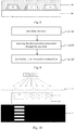
- FIG. 1 is a partial flowchart of a method for manufacturing a color filter substrate in accordance with an embodiment of the present disclosure.
- a substrate is provided; in step S108, a photosensitive composition for forming a color resist is applied on the substrate; and in step S110, the photosensitive composition is patterned to form at least two color resists having different colors.
- FIG. 2 is a schematic cross-sectional view of a color filter substrate after applying a photosensitive composition in accordance with a method of an embodiment of the present disclosure.
- FIG. 3 is a schematic cross-sectional view of a color filter substrate after forming a first color resist, a second color resist, and a third color resist in accordance with a method of an embodiment of the present disclosure.
- the photosensitive composition 100 is applied on the substrate 200.
- the photosensitive composition 100 is patterned to form the first, second, and third color resists 111, 121, and 131.
- the photosensitive composition 100 has been described in detail above and will not be described again.
- the first, second, and third color resists 111, 121, and 131 are red, green, and blue color resists, respectively.
- the patterning in step S110 may include: providing at least two masks having different pattern configurations; exposing the photosensitive composition by using light of different wavelengths, respectively, through corresponding one of the at least two masks, wherein the wavelengths of the light used for each exposure are different from each other; and developing the photosensitive composition to form the at least two color resists.
- FIG. 4 is a flowchart of a method for patterning a photosensitive composition in accordance with a method of an embodiment of the present disclosure.
- step S110 in FIG. 1 may include: in step S1101, providing at least two masks; in step S1102, exposing the photosensitive composition through the at least two masks; and in step S1103, developing the photosensitive composition.
- FIGS. 5 to 7 are schematic views of exposing a photosensitive composition in accordance with a method of an embodiment of the present disclosure.
- a first mask 710 having a first pattern is provided.
- An opening pattern is only designed at a position, of the first mask 710, corresponding to a first region 110 where the first color resist 111 is to be formed.
- the photosensitive composition 100 within the first region 110 is irradiated with a first ultraviolet light.
- the first photoinitiator, in the photosensitive composition 100 within the first region 110 is decomposed under the irradiation of the first ultraviolet light to generate a first active species.
- the first active species initiates the polymerization of the first color resist precursor, such that the first color resist precursor is deposited, thereby the first color resist 111 is formed.
- a second mask 720 having a second pattern is provided.
- An opening pattern is only designed at a position, of the second mask 720, corresponding to a second region 120 where the second color resist 121 is to be formed.
- the photosensitive composition 100 within the second region 120 is irradiated with a second ultraviolet light.
- the second photoinitiator, in the photosensitive composition 100 within the second region 120 is decomposed under the irradiation of the second ultraviolet light to generate a second active species.
- the second active species initiates the polymerization of the second color resist precursor, such that the second color resist precursor is deposited, thereby the second color resist 121 is formed.
- a third mask 730 having a third pattern is provided.
- An opening pattern is only designed at a position, of the third mask 730, corresponding to a third region 130 where the third color resist 131 is to be formed.
- the photosensitive composition 100 within the third region 130 is irradiated with a third ultraviolet light.
- the third photoinitiator, in the photosensitive composition 100 within the third region 130 is decomposed under the irradiation of the third ultraviolet light to generate a third active species.
- the third active species initiates the polymerization of the third color resist precursor, such that the third color resist precursor is deposited, thereby the third color resist 131 is formed.
- the designed patterns of the first, second, and third masks may be the same or different, which is not specifically limited in this disclosure.
- the first ultraviolet light can only make the first photoinitiator corresponding to it decompose to generate the first active species.
- the second ultraviolet light can only make the second photoinitiator corresponding to it decompose to generate the second active species.
- the third ultraviolet light can only make the third photoinitiator corresponding to it decompose to generate the third active species.
- the first active species can only polymerize with its corresponding first color resist precursor.
- the second active species can only polymerize with its corresponding second color resist precursor.
- the third active species can only polymerize with its corresponding third color resist precursor.
- the first photoinitiator is isopropyl thioxanthone (as shown in the above formula (5))
- the first active species generated by the decomposing of isopropyl thioxanthone under the irradiation of the first ultraviolet light, having the wavelength from about 380 nm to about 400 nm is an isopropyl thioxanthone intermediate, the structural formula of which is as shown in the following formula (6).
- the second photoinitiator is Ar 3 SKCl
- the second active species generated by the decomposing of Ar 3 SKCl under the irradiation of the second ultraviolet light, having the wavelength from about 244 nm to about 264 nm is KCl-OH.
- the third photoinitiator is Ar 2 IBF 6 or Ar 2 ISbF 6
- Ar is the aryl.
- first, second, and third active species are only present during the polymerization process and are not present separately in the final product.
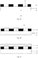
- FIG. 8 is a schematic cross-sectional view of a color filter substrate exposed in accordance with a method of an embodiment of the present disclosure. As shown in FIG. 8 , the first, second, and third color resist precursors in which the polymerization occurs are deposited to form the first, second, and third color resists 111, 121, and 131.
- step S1103 the unexposed portion of the photosensitive composition 100 in FIG. 8 is developed, thereby a structure as shown in FIG. 3 is formed.
- the patterning in step S110 may include: providing one mask; exposing the photosensitive composition N times through the one mask, wherein N is equal to the number of the at least two photoinitiators; and developing the photosensitive composition to form the at least two color resists.
- the wavelengths of light used for each exposure are different from each other.
- the one mask is moved in a given direction with a given step between two exposures.
- FIG. 9 is a flowchart of a method for patterning a photosensitive composition in accordance with a method of an embodiment of the present disclosure.
- step S110 in FIG. 1 may include: in step S1101', providing one mask; in step S1102', exposing the photosensitive composition through the one mask; and in step S1103', developing the photosensitive composition.
- the mask may have a lateral dimension larger than a lateral dimension of the color filter substrate to be manufactured.
- the pattern of the mask is suitable for the color resists having different colors.
- FIGS. 10 to 12 are schematic views of exposing a photosensitive composition in accordance with a method of an embodiment of the present disclosure.
- a fourth mask having a fourth pattern is provided.
- the photosensitive composition was exposed N times through the fourth mask, where N is equal to the number of the at least two photoinitiators.
- the photosensitive composition is exposed three times through the fourth mask.
- a fourth mask 740 having a fourth pattern is provided.
- An opening of the fourth mask 740 is aligned with the first region 110 where the first color resist 111 is to be formed.
- the photosensitive composition 100 within the first region 110 is irradiated with the first ultraviolet light.
- the first photoinitiator, in the photosensitive composition 100 within the first region 110 is decomposed under the irradiation of the first ultraviolet light to generate the first active species.
- the first active species then initiates the polymerization of the first color resist precursor, such that the first color resist precursor is deposited, thereby the first color resist 111 is formed.
- the opening of the fourth mask 740 is aligned with the second region 120 where the second color resist 121 is to be formed.
- the photosensitive composition 100 within the second region 120 is irradiated with the second ultraviolet light.
- the second photoinitiator, in the photosensitive composition 100 within the second region 120 is decomposed under the irradiation of the second ultraviolet light to generate the second active species.
- the second active species then initiates the polymerization of the second color resist precursor, such that the second color resist precursor is deposited, thereby the second color resist 121 is formed.
- the opening of the fourth mask 740 is aligned with the third region 130 where the third color resist 131 is to be formed.
- the photosensitive composition 100 in the third region 130 is irradiated with the third ultraviolet light.
- the third photoinitiator, in the photosensitive composition 100 within the third region 130 is decomposed under the irradiation of the third ultraviolet light to generate the third active species.
- the third active species then initiates the polymerization of the third color resist precursor, such that the third color resist precursor is deposited, thereby the third color resist 131 is formed.
- the structure as shown in FIG. 8 is obtained. That is, the first, second, and third color resist precursors in which the polymerization occurs are deposited to form the first, second, and third color resists 111, 121, and 131.
- step S1103' the unexposed portion of the photosensitive composition 100 in FIG. 8 is developed, thereby the structure shown in FIG. 3 is formed.
- the fourth mask is moved in a given direction with a given step length between two exposures.
- the present disclosure does not specifically limit the size of the step and the specific moving direction. The size of the step and the moving direction can be determined according to actual needs.
- FIG. 13 is a flowchart of a method for manufacturing a color filter substrate in accordance with an embodiment of the present disclosure. As shown in FIG. 13 , after step S101 and before step S108, the method further includes: in step S104, forming an ITO layer on a first side of the substrate; and in step S106, forming a black matrix on a second side of the substrate.
- FIG. 14 is a schematic cross-sectional view of a color filter substrate after forming an ITO layer in accordance with a method of an embodiment of the present disclosure.
- FIG. 15 is a schematic cross-sectional view of a color filter substrate after forming a black matrix in accordance with a method of an embodiment of the present disclosure.
- an ITO layer 300 is formed on a first side 2001 of the substrate 200.
- the first side 2001 is the opposite side of a side on which the photosensitive composition is to be applied.
- a patterned black matrix 400 is formed on a second side 2002 of the substrate 200.
- the second side 2002 is a side on which the photosensitive composition is to be applied.
- FIG. 16 is a schematic cross-sectional view of a color filter substrate after forming a first color resist, a second color resist, and a third color resist in accordance with a method of an embodiment of the present disclosure. Specifically, as shown in FIG. 16 , a first color resist 111, a second color resist 121, and a third color resist 131 are formed on the second side 2002 of the substrate 200 and on the black matrix 400.
- step S110 that is, after forming the at least two color resists
- the method further includes: in S112, forming a planarization layer on the at least two color resists and the black matrix; and in S114, forming a support pillar on the planarization layer.
- FIG. 17 is a schematic cross-sectional view of a color filter substrate after forming a planarization layer in accordance with a method of an embodiment of the present disclosure.
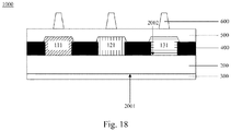
- FIG. 18 is a schematic cross-sectional view of a color filter substrate after forming a support pillar in accordance with a method of an embodiment of the present disclosure.
- a planarization layer 500 is formed on the first, second, and third color resists 111, 121, and 131 and on the black matrix 400.
- a patterned support pillar 600 is formed on the planarization layer 500.
- a color filter substrate is also provided.
- the color filter substrate is manufactured by the method for manufacturing a color filter substrate as described above.
- the color filter substrate 1000 includes: a substrate 200; an ITO layer 300 on a first side 2001 of the substrate 200; a black matrix 400 on the second side 2002 of the substrate 200; a first color resist 111, a second color resist 121, and a third color resist 131 on the second side of the substrate 200 and on the black matrix 400; a planarization layer 500 on the black matrix 400 and the first, second, and third color resists 111, 121, and 131; and a support pillar 600 on the planarization layer 500.
- a photosensitive composition for forming a color resist is provided.
- the photosensitive composition is used for manufacturing the color resist, it is only necessary to apply a color resist material once, and the color resists having different colors can be obtained by one-time developing how many times being exposed.
- a method for manufacturing a color filter substrate which utilizes the above-described photosensitive composition to form color resists having different colors, thereby simplifying the process of manufacturing a color filter substrate and saving manufacturing costs.
Landscapes
- Physics & Mathematics (AREA)
- General Physics & Mathematics (AREA)
- Nonlinear Science (AREA)
- Engineering & Computer Science (AREA)
- Optics & Photonics (AREA)
- Chemical & Material Sciences (AREA)
- Architecture (AREA)
- Structural Engineering (AREA)
- Spectroscopy & Molecular Physics (AREA)
- Crystallography & Structural Chemistry (AREA)
- Mathematical Physics (AREA)
- Manufacturing & Machinery (AREA)
- Electromagnetism (AREA)
- Inorganic Chemistry (AREA)
- Materials For Photolithography (AREA)
- Optical Filters (AREA)
Abstract
Description
- This application claims priority of China Patent Application No.
201711341225.3, filed on December 14, 2017 - Embodiments of the present disclosure relate to the field of display technologies, and in particular, to a photosensitive composition for forming color resist, a method for manufacturing a color filter substrate, and a color filter substrate.
- Thin film transistor liquid crystal display (TFT-LCD) is an important planner display device. With the development of the manufacturing technology of displays, the liquid crystal display has developed rapidly, has gradually replaced the traditional kinescope display, and becomes the mainstream of future planner display. Due to the advantages of light weight, small size, no radiation, good energy saving effect, high resolution, etc., liquid crystal displays are widely used in televisions, computers, mobile phones and other fields.
- Embodiments of the present disclosure provide a photosensitive composition for forming a color resist, a method for manufacturing a color filter substrate, and a color filter substrate.
- According to a first aspect of an embodiment of the present disclosure, there is provided a photosensitive composition for forming a color resist, including: at least two color resist precursors; and at least two photoinitiators. Each of the at least two photoinitiators is used to initiate polymerization of a corresponding one color resist precursor, of the at least two color resist precursors, to form the color resist.
- In an embodiment of the present disclosure, sensitive wavelengths of the at least two photoinitiators are different from each other.
- In an embodiment of the present disclosure, the sensitive wavelengths of the at least two photoinitiators are in an ultraviolet range.
- In an embodiment of the present disclosure, the at least two color resist precursors comprise a monomer material.
- In an embodiment of the present disclosure, the at least two color resist precursors comprise a first color resist precursor, a second color resist precursor, and a third color resist precursor, and the at least two photoinitiators comprise a first photoinitiator corresponding to the first color resist precursor, a second photoinitiator corresponding to the second color resist precursor, and a third photoinitiator corresponding to the third color resist precursor.
- In an embodiment of the present disclosure, the first color resist precursor is formed by binding a first base monomer material with a first pigment, the first base monomer material comprising CH2=CHCOOR1, R1 of which is a first group for binding a molecule of the first pigment, and wherein the second color resist precursor is formed by binding a second base monomer material with a second pigment, the second base monomer material comprising CR'R2=C(CN)2, R2 of which is a second group for binding a molecule of the second pigment, and wherein the third color resist precursor is formed by binding a third base monomer material with a third pigment, the third base monomer material comprising CR'R3=CH2, R3 of which is a third group for binding a molecule of the third pigment. R' is a phenyl. The first photoinitiator comprises a thioxanthone molecule, the second photoinitiator comprises a triarylsulfonium salt, and the third photoinitiator comprises a diaryl iodonium salt.
- In an embodiment of the present disclosure, the first photoinitiator comprises isopropyl thioxanthone, the second photoinitiator comprises Ar3SKCl, and the third photoinitiator comprises Ar2IBF6 or Ar2ISbF6, wherein Ar is an aryl.
- In an embodiment of the present disclosure, the first group is MgBr, and the first pigment comprises a pigment R254; the second group is R"OZn, and the second pigment comprises a pigment G58; and the third group is R"OCu, and the third pigment comprises a pigment B 15:6, wherein R" is an alkyl.
- According to a second aspect of an embodiment of the present disclosure, there is provided a method for manufacturing a color filter substrate, including: providing a substrate; applying a photosensitive composition for forming a color resist on the substrate; and patterning the photosensitive composition to form at least two color resists. The photosensitive composition comprises at least two color resist precursors and at least two photoinitiators. Each of the at least two photoinitiators is used to initiate polymerization of a corresponding one color resist precursor, of the at least two color resist precursors, to form the color resist.
- In an embodiment of the present disclosure, sensitive wavelengths of the at least two photoinitiators are different from each other.
- In an embodiment of the present disclosure, the sensitive wavelengths of the at least two photoinitiators are in an ultraviolet range.
- In an embodiment of the present disclosure, the patterning comprises: providing at least two masks having different pattern configurations; exposing the photosensitive composition by using light of different wavelengths, respectively, through corresponding one of the at least two masks, wherein the wavelengths of the light used for each exposure are different from each other; and developing the photosensitive composition to form the at least two color resists.
- In an embodiment of the present disclosure, the patterning comprises: providing one mask; exposing the photosensitive composition N times through the one mask, wherein N is equal to a number of the at least two photoinitiators; and developing the photosensitive composition to form the at least two color resists. The wavelengths of the light used for each exposure are different from each other. The one mask is moved in a given direction with a given step between two exposures.
- In an embodiment of the present disclosure, the at least two color resist precursors comprise a monomer material.
- In an embodiment of the present disclosure, the at least two color resist precursors comprise a first color resist precursor, a second color resist precursor, and a third color resist precursor, and the at least two photoinitiators comprise a first photoinitiator corresponding to the first color resist precursor, a second photoinitiator corresponding to the second color resist precursor, and a third photoinitiator corresponding to the third color resist precursor.
- In an embodiment of the present disclosure, the first color resist precursor is formed by binding a first base monomer material with a first pigment, the first base monomer material comprising CH2=CHCOOR1, R1 of which is a first group for binding a molecule of the first pigment, and wherein the second color resist precursor is formed by binding a second base monomer material with a second pigment, the second base monomer material comprising CR'R2=C(CN)2, R2 of which is a second group for binding a molecule of the second pigment, and wherein the third color resist precursor is formed by binding a third base monomer material with a third pigment, the third base monomer material comprising CR'R3=CH2, R3 of which is a third group for binding a molecule of the third pigment. R' is a phenyl. The first photoinitiator comprises a thioxanthone molecule, the second photoinitiator comprises a triarylsulfonium salt, and the third photoinitiator comprises a diaryl iodonium salt.
- In an embodiment of the present disclosure, the first group is MgBr, and the first pigment comprises a pigment R254; the second group is R"OZn, and the second pigment comprises a pigment G58; and the third group is R"OCu, and the third pigment comprises a pigment B 15:6, wherein R" is an alkyl.
- In an embodiment of the present disclosure, the method further includes: before applying the photosensitive composition, forming an ITO layer on an opposite side of a side, on which the photosensitive composition is to be applied, of the substrate; and forming a patterned black matrix on the side of the substrate.
- In an embodiment of the present disclosure, the method further includes: after forming the at least two color resists, forming a planarization layer on a top surface of a structure as formed; and forming a support pillar on the planarization layer.
- According to a third aspect of an embodiment of the present disclosure, a color filter substrate is provided. The color filter substrate is manufactured by a method for manufacturing a color filter substrate according to the second aspect of the embodiments of the present disclosure.
- In an embodiment of the present disclosure, a photosensitive composition for forming a color resist is provided. Further aspects and regions of applicability will become apparent from the description provided herein. It should be understood that various aspects of this disclosure may be implemented individually or in combination with one or more other aspects. It should also be understood that the description and specific examples herein are intended for purposes of view only and are not intended to limit the scope of the present disclosure.
- The drawings described herein are for illustrative purposes only of selected embodiments and not all possible implementations, and are not intended to limit the scope of the present disclosure.
-
FIG. 1 is a partial flowchart of a method for manufacturing a color filter substrate in accordance with an embodiment of the present disclosure; -
FIG. 2 is a schematic cross-sectional view of a color filter substrate after applying a photosensitive composition in accordance with a method of an embodiment of the present disclosure; -
FIG. 3 is a schematic cross-sectional view of a color filter substrate after forming a first color resist, a second color resist, and a third color resist in accordance with a method of an embodiment of the present disclosure; -
FIG. 4 is a flowchart of a method for patterning a photosensitive composition in accordance with a method of an embodiment of the present disclosure; -
FIG. 5 is a schematic view of exposing a photosensitive composition in accordance with a method of an embodiment of the present disclosure; -
FIG. 6 is a schematic view of exposing a photosensitive composition in accordance with a method of an embodiment of the present disclosure; -
FIG. 7 is a schematic view of exposing a photosensitive composition in accordance with a method of an embodiment of the present disclosure; -
FIG. 8 is a schematic cross-sectional view of a color filter substrate exposed in accordance with a method of an embodiment of the present disclosure; -
FIG. 9 is a flowchart of a method for patterning a photosensitive composition in accordance with a method of an embodiment of the present disclosure; -
FIG. 10 is a schematic view of exposing a photosensitive composition in accordance with a method of an embodiment of the present disclosure; -
FIG. 11 is a schematic view of exposing a photosensitive composition in accordance with a method of an embodiment of the present disclosure; -
FIG. 12 is a schematic view of exposing a photosensitive composition in accordance with a method of an embodiment of the present disclosure; -
FIG. 13 is a flowchart of a method for manufacturing a color filter substrate in accordance with an embodiment of the present disclosure; -
FIG. 14 is a schematic cross-sectional view of a color filter substrate after forming an ITO layer in accordance with a method of an embodiment of the present disclosure; -
FIG. 15 is a schematic cross-sectional view of a color filter substrate after forming a black matrix in accordance with a method of an embodiment of the present disclosure; -
FIG. 16 is a schematic cross-sectional view of a color filter substrate after forming a first color resist, a second color resist, and a third color resist in accordance with a method of an embodiment of the present disclosure; -
FIG. 17 is a schematic cross-sectional view of a color filter substrate after forming a planarization layer in accordance with a method of an embodiment of the present disclosure; and -
FIG. 18 is a schematic cross-sectional view of a color filter substrate after forming a support pillar in accordance with a method of an embodiment of the present disclosure. - Corresponding reference numerals indicate corresponding parts or features throughout the several views of the drawings.
- As used herein and in the appended claims, the singular form of a word includes the plural, and vice versa, unless the context clearly dictates otherwise. Thus, the references "a", "an", and "the" are generally inclusive of the plurals of the respective terms. Similarly, the words "comprise", "comprises", and "comprising" are to be interpreted inclusively rather than exclusively. Likewise, the terms "include", "including" and "or" should all be construed to be inclusive, unless such a construction is clearly prohibited from the context. Where used herein the term "examples," particularly when followed by a listing of terms is merely exemplary and illustrative, and should not be deemed to be exclusive or comprehensive.
- In addition, it should be noted that, in the description of the present disclosure, the orientations or positions relationship indicated by the terms "upper", "above", "lower", "under", "top", "bottom", "between", etc. are the orientations or positions relationship based on the orientations or positions relationship shown in the drawings, which is merely for the convenience of describing the present disclosure and the simplifing the description, and does not indicate or imply that the referred device or element has to have a specific orientation and is constructed and operated in a specific orientation, therefore, it can not be understood as a limitation to the disclosure. In addition, when an element or a layer is referred to as being "on" another element or layer, the element or the layer can be directly on the another element or layer, or an intermediate element or layer can be present; likewise, when an element or a layer is referred to as being "under" another element or layer, the element or the layer can be directly under another element or layer, or at least one intermediate element or layer can be present; when an element or a layer is referred to as being between two elements or two layers, the element or the layer can be an unique element or layer between the two elements or the two layers, or more than one intermediate element or layer can be present.
- The flowchart depicted herein are just one example. There may be many variations to this view or the steps described therein without departing from the spirit of the invention. For instance, the steps may be performed in a differing order or steps may be added, deleted or modified. All of these variations are considered a part of the claimed invention.
- Example embodiments will now be described more fully with reference to the accompanying drawings.
- At present, when manufacturing a color resist of a color filter substrate, it is necessary to deposit the color resist material multiple times and develop multiple times to finally obtain the color resist, and the process is complicate.
- In an embodiment of the present disclosure, a photosensitive composition for forming a color resist is provided. When the photosensitive composition is used for manufacturing a color resist, it is only necessary to apply the color resist material once, and the color resist having different colors can be obtained by one-time developing regardless of how many times being exposed. Thus, the process for manufacturing the color resist can be simplified. Thereby, the process for manufacturing the color filter substrate can be simplified, and the manufacturing cost can be saved.
- The photosensitive composition according to an embodiment of the present disclosure may include at least two color resist precursors and at least two photoinitiators. As used herein, the color resist precursor refers to a material capable of forming the color resist by polymerization. Each of the at least two photoinitiators is used to initiate polymerization of a corresponding one color resist precursor, of the at least two color resist precursors, to form the color resist. That is, the photoinitiator is in one-to-one correspondence with the color resist precursor. One photoinitiator can only initiates polymerization of one corresponding color resist precursor.
- Specifically, in an embodiment of the present disclosure, the at least two color resist precursors may include a first color resist precursor, a second color resist precursor, and a third color resist precursor. The at least two photoinitiators may include a first photoinitiator corresponding to the first color resist precursor, a second photoinitiator corresponding to the second color resist precursor, and a third photoinitiator corresponding to the third color resist precursor. It should be understood that the number of types of the color resist precursors disclosed in the embodiments of the present disclosure is merely exemplary and should not be construed as a limit to the disclosure. That is, the number of types of the color resist precursors may be two, three or more.
- In an embodiment of the present disclosure, the photosensitive composition includes: a first color resist precursor; a first photoinitiator corresponding to the first color resist precursor; a second color resist precursor; a second photoinitiator corresponding to the second color resist precursor; a third color resist precursor; and a third photoinitiator corresponding to the third color resist precursor. It is understood that the ratio of the color resist precursor to the photoinitiator in the photosensitive composition of the present disclosure can be determined according to actual needs, for example, according to the thickness of the color filter or the like. In an embodiment of the present disclosure, the first, second, and third color resist precursors and the first, second, and third photoinitiators are uniformly mixed to obtain the photosensitive composition. Further, the photosensitive composition of the present disclosure may further include a appropriate organic solvent. The color resist precursors, the photoinitiators, and the appropriate organic solvent are soluble with each other and are uniformly mixed to obtain the photosensitive composition.
- In an exemplary embodiment of the present disclosure, the first, second, and third color resist precursors may include a monomer material. The first color resist precursor is formed by binding a first base monomer material with a first pigment. In an exemplary embodiment of the present disclosure, the first base monomer material may be an acrylic monomer having a chemical formula of CH2=CHCOOR1, wherein R1 is a first group for binding a molecule of the first pigment. The second color resist precursor is formed by binding a second base monomer material with a second pigment. In an exemplary embodiment of the present disclosure, the second base monomer material may be a vinylidene cyanide monomer having a chemical formula of CR'R2=C(CN)2, wherein R2 is a second group for binding a molecule of the second pigment. The third color resist precursor is formed by binding a third base monomer material with a third pigment. In an exemplary embodiment of the present disclosure, the third base monomer material may be an α-olefin monomer having a chemical formula of CR'R3=CH2, wherein R3 is a third group for binding a molecule of the third pigment. It is to be noted that R' in the above chemical formula is a phenyl.
- It should be noted that, in an exemplary embodiment of the present disclosure, the first, second, and third pigments are, for example, red, green, and blue pigments, respectively.
- In an exemplary embodiment of the present disclosure, the first group R1 may be MgBr; the first pigment may include a pigment R254, i.e., 3,6-Bis(4-chlorophenyl)-2,5-dihydro-pyrrolo[3,4-c]pyrrole-1,4-dione having a molecular formula of C18H10O2N2Cl2, the structural formula of which is as shown in the following formula (1);

- The second group R2 may be R"OZn, wherein R" is an organic group, and specifically, R" may be an alkyl; the second pigment may include G58 having a molecular formula of C32N8Cl4Br12Zn, the structural formula of which is as shown in the following formula (2) ;

- The third group R3 may be R"OCu, wherein, as described above, R" is the organic group, and specifically, R" may be the alkyl; the third pigment may include B15:6 having a molecular formula of C32H16N8Cu, the structural formula of which is as shown in the following formula (3).

- It should be noted that, the first color resist precursor is obtained by binding the first base monomer material with the first pigment, the second color resist precursor is obtained by binding the second base monomer material with the second pigment, and the third color resist precursor is obtained by binding the third base monomer material with the third pigment. Specifically, the first color resist precursor is obtained by binding the first group R1 in CH2=CHCOOR1 with the molecule of the first pigment, that is, obtained by an addition reaction of MgBr with a carbonyl in the pigment R254 (as shown in the above formula (1)). The second color resist precursor is obtained by binding the second group R2 in CR'R2=C(CN)2 with the molecule of the second pigment, that is, obtained by a Zn-Zn metallic bond formed by R"OZn with complex metal Zn atoms in the pigment G58 (as shown in the above formula (2)). The third color resist precursor is obtained by binding the third group R3 in CR'R3=CH2 with the molecule of the third pigment, that is, obtained by a Cu-Cu metallic bond formed by R"OCu with complex Cu atoms in the pigment B15:6 (as shown in the above formula (3)).
- In an exemplary embodiment of the present disclosure, the first photoinitiator capable of initiating polymerization of the above-described first color resist precursor is a thioxanthone molecule, the structural formula of which is as shown in the following formula (4).

- As an example, the second photoinitiator may be Ar3SKCl or Ar3SMgBr. The third photoinitiator may be Ar3SPF6, Ar3SClO4, Ar2IBF6 or Ar2ISbF6.
- As a specific example, the first photoinitiator is an isopropyl thioxanthone, the structural formula of which is as shown in the following formula (5).

- The second photoinitiator is Ar3SKCl. When Ar is a benzene ring, the second photoinitiator is C18H15SKCl, the name of which is Triphenylsulfonium potassium chloride. The third photoinitiator is Ar2IBF6 or Ar2ISbF6. When Ar is a benzene ring, the third photoinitiator is C12H10IBF6, the name of which is diphenyliodonium fluoroborate, or C12H10ISbF6, the name of which is diphenyliodonium hexafluoroantion.
- It should be noted that the sensitive wavelengths of the first, second and third photoinitiators are different from each other. It should be understood that herein, the sensitive wavelength refers to the wavelength of light that is capable of initiating a chemical reaction of the photoinitiator. For example, a photoinitiator undergoes a decomposing reaction under excitation of light having a sensitive wavelength, to generate a decomposed product such as a free radical, a cation or an anion. As an example, the sensitive wavelengths of the first, second and third photoinitiators are in the ultraviolet range. It should be understood that herein, the ultraviolet range refers to the range of ultraviolet light having a wavelength of light of from about 10 nm to about 400 nm.
- In an exemplary embodiment of the present disclosure, a method for manufacturing a color filter substrate is also provided. The method can simplify the process of manufacturing the color filter substrate and save manufacturing cost.
- A method for manufacturing a color filter substrate according to an embodiment of the present disclosure will be described in detail below with reference to
FIGS. 1 to 18 . -
FIG. 1 is a partial flowchart of a method for manufacturing a color filter substrate in accordance with an embodiment of the present disclosure. As shown inFIG. 1 , in step S101, a substrate is provided; in step S108, a photosensitive composition for forming a color resist is applied on the substrate; and in step S110, the photosensitive composition is patterned to form at least two color resists having different colors. -
FIG. 2 is a schematic cross-sectional view of a color filter substrate after applying a photosensitive composition in accordance with a method of an embodiment of the present disclosure.FIG. 3 is a schematic cross-sectional view of a color filter substrate after forming a first color resist, a second color resist, and a third color resist in accordance with a method of an embodiment of the present disclosure. Specifically, as shown inFIG. 2 , thephotosensitive composition 100 is applied on thesubstrate 200. As shown inFIG. 3 , thephotosensitive composition 100 is patterned to form the first, second, and third color resists 111, 121, and 131. It should be noted that, thephotosensitive composition 100 has been described in detail above and will not be described again. It should be noted that, in an exemplary embodiment of the present disclosure, the first, second, and third color resists 111, 121, and 131 are red, green, and blue color resists, respectively. - On one hand, the patterning in step S110 may include: providing at least two masks having different pattern configurations; exposing the photosensitive composition by using light of different wavelengths, respectively, through corresponding one of the at least two masks, wherein the wavelengths of the light used for each exposure are different from each other; and developing the photosensitive composition to form the at least two color resists.
- Next, a specific process of patterning the photosensitive composition will be described.
-
FIG. 4 is a flowchart of a method for patterning a photosensitive composition in accordance with a method of an embodiment of the present disclosure. As shown inFIG. 4 , step S110 inFIG. 1 may include: in step S1101, providing at least two masks; in step S1102, exposing the photosensitive composition through the at least two masks; and in step S1103, developing the photosensitive composition. -
FIGS. 5 to 7 are schematic views of exposing a photosensitive composition in accordance with a method of an embodiment of the present disclosure. Specifically, inFIG. 5 , afirst mask 710 having a first pattern is provided. An opening pattern is only designed at a position, of thefirst mask 710, corresponding to afirst region 110 where the first color resist 111 is to be formed. At the time of exposing, thephotosensitive composition 100 within thefirst region 110 is irradiated with a first ultraviolet light. Thus, the first photoinitiator, in thephotosensitive composition 100 within thefirst region 110, is decomposed under the irradiation of the first ultraviolet light to generate a first active species. The first active species initiates the polymerization of the first color resist precursor, such that the first color resist precursor is deposited, thereby the first color resist 111 is formed. - In
FIG. 6 , asecond mask 720 having a second pattern is provided. An opening pattern is only designed at a position, of thesecond mask 720, corresponding to asecond region 120 where the second color resist 121 is to be formed. At the time of exposing, thephotosensitive composition 100 within thesecond region 120 is irradiated with a second ultraviolet light. Thus, the second photoinitiator, in thephotosensitive composition 100 within thesecond region 120, is decomposed under the irradiation of the second ultraviolet light to generate a second active species. The second active species initiates the polymerization of the second color resist precursor, such that the second color resist precursor is deposited, thereby the second color resist 121 is formed. - In
FIG. 7 , athird mask 730 having a third pattern is provided. An opening pattern is only designed at a position, of thethird mask 730, corresponding to athird region 130 where the third color resist 131 is to be formed. At the time of exposing, thephotosensitive composition 100 within thethird region 130 is irradiated with a third ultraviolet light. Thus, the third photoinitiator, in thephotosensitive composition 100 within thethird region 130, is decomposed under the irradiation of the third ultraviolet light to generate a third active species. The third active species initiates the polymerization of the third color resist precursor, such that the third color resist precursor is deposited, thereby the third color resist 131 is formed. - It should be noted that the designed patterns of the first, second, and third masks may be the same or different, which is not specifically limited in this disclosure.
- It should be noted that the wavelengths of the first, second, and third ultraviolet lights are different from each other. The first ultraviolet light can only make the first photoinitiator corresponding to it decompose to generate the first active species. The second ultraviolet light can only make the second photoinitiator corresponding to it decompose to generate the second active species. The third ultraviolet light can only make the third photoinitiator corresponding to it decompose to generate the third active species. In addition, the first active species can only polymerize with its corresponding first color resist precursor. The second active species can only polymerize with its corresponding second color resist precursor. The third active species can only polymerize with its corresponding third color resist precursor.
- According to the foregoing, in an exemplary embodiment of the present disclosure, when the first photoinitiator is isopropyl thioxanthone (as shown in the above formula (5)), the first active species generated by the decomposing of isopropyl thioxanthone under the irradiation of the first ultraviolet light, having the wavelength from about 380 nm to about 400 nm, is an isopropyl thioxanthone intermediate, the structural formula of which is as shown in the following formula (6).

- When the second photoinitiator is Ar3SKCl, the second active species generated by the decomposing of Ar3SKCl under the irradiation of the second ultraviolet light, having the wavelength from about 244 nm to about 264 nm, is KCl-OH. When the third photoinitiator is Ar2IBF6 or Ar2ISbF6, the third active species generated by the decomposing of Ar2IBF6 or Ar2ISbF6 under the irradiation of the third ultraviolet light, having the wavelength from about 217 nm to about 237 nm, is HBF6 or HSbF6. As described above, Ar is the aryl.
- It should be noted that the above first, second, and third active species are only present during the polymerization process and are not present separately in the final product.
-
FIG. 8 is a schematic cross-sectional view of a color filter substrate exposed in accordance with a method of an embodiment of the present disclosure. As shown inFIG. 8 , the first, second, and third color resist precursors in which the polymerization occurs are deposited to form the first, second, and third color resists 111, 121, and 131. - Then, as described in step S1103, the unexposed portion of the
photosensitive composition 100 inFIG. 8 is developed, thereby a structure as shown inFIG. 3 is formed. - On the other hand, in the case where the patterns of the color resists having different colors to be manufactured are the same, the patterning in step S110 may include: providing one mask; exposing the photosensitive composition N times through the one mask, wherein N is equal to the number of the at least two photoinitiators; and developing the photosensitive composition to form the at least two color resists. The wavelengths of light used for each exposure are different from each other. The one mask is moved in a given direction with a given step between two exposures.
- Next, a specific process of patterning the photosensitive composition will be described.
-
FIG. 9 is a flowchart of a method for patterning a photosensitive composition in accordance with a method of an embodiment of the present disclosure. As shown inFIG. 9 , step S110 inFIG. 1 may include: in step S1101', providing one mask; in step S1102', exposing the photosensitive composition through the one mask; and in step S1103', developing the photosensitive composition. - It should be noted that only one mask is used in this embodiment, and the mask may have a lateral dimension larger than a lateral dimension of the color filter substrate to be manufactured. The pattern of the mask is suitable for the color resists having different colors.
-
FIGS. 10 to 12 are schematic views of exposing a photosensitive composition in accordance with a method of an embodiment of the present disclosure. In an exemplary embodiment of the present disclosure, a fourth mask having a fourth pattern is provided. The photosensitive composition was exposed N times through the fourth mask, where N is equal to the number of the at least two photoinitiators. As an example, the photosensitive composition is exposed three times through the fourth mask. - Specifically, in
FIG. 10 , afourth mask 740 having a fourth pattern is provided. An opening of thefourth mask 740 is aligned with thefirst region 110 where the first color resist 111 is to be formed. Thephotosensitive composition 100 within thefirst region 110 is irradiated with the first ultraviolet light. Thus, the first photoinitiator, in thephotosensitive composition 100 within thefirst region 110, is decomposed under the irradiation of the first ultraviolet light to generate the first active species. The first active species then initiates the polymerization of the first color resist precursor, such that the first color resist precursor is deposited, thereby the first color resist 111 is formed. - In
FIG. 11 , the opening of thefourth mask 740 is aligned with thesecond region 120 where the second color resist 121 is to be formed. Thephotosensitive composition 100 within thesecond region 120 is irradiated with the second ultraviolet light. Thus, the second photoinitiator, in thephotosensitive composition 100 within thesecond region 120, is decomposed under the irradiation of the second ultraviolet light to generate the second active species. The second active species then initiates the polymerization of the second color resist precursor, such that the second color resist precursor is deposited, thereby the second color resist 121 is formed. - In
FIG. 12 , the opening of thefourth mask 740 is aligned with thethird region 130 where the third color resist 131 is to be formed. Thephotosensitive composition 100 in thethird region 130 is irradiated with the third ultraviolet light. Thus, the third photoinitiator, in thephotosensitive composition 100 within thethird region 130, is decomposed under the irradiation of the third ultraviolet light to generate the third active species. The third active species then initiates the polymerization of the third color resist precursor, such that the third color resist precursor is deposited, thereby the third color resist 131 is formed. - Thereby, the structure as shown in
FIG. 8 is obtained. That is, the first, second, and third color resist precursors in which the polymerization occurs are deposited to form the first, second, and third color resists 111, 121, and 131. - Then, as described in step S1103', the unexposed portion of the
photosensitive composition 100 inFIG. 8 is developed, thereby the structure shown inFIG. 3 is formed. - It should be noted that the fourth mask is moved in a given direction with a given step length between two exposures. The present disclosure does not specifically limit the size of the step and the specific moving direction. The size of the step and the moving direction can be determined according to actual needs.
- It should be noted that the process of exposing has been described in detail in the text above and will not be described here.
-
FIG. 13 is a flowchart of a method for manufacturing a color filter substrate in accordance with an embodiment of the present disclosure. As shown inFIG. 13 , after step S101 and before step S108, the method further includes: in step S104, forming an ITO layer on a first side of the substrate; and in step S106, forming a black matrix on a second side of the substrate. -
FIG. 14 is a schematic cross-sectional view of a color filter substrate after forming an ITO layer in accordance with a method of an embodiment of the present disclosure.FIG. 15 is a schematic cross-sectional view of a color filter substrate after forming a black matrix in accordance with a method of an embodiment of the present disclosure. As shown inFIG. 14 , anITO layer 300 is formed on afirst side 2001 of thesubstrate 200. Thefirst side 2001 is the opposite side of a side on which the photosensitive composition is to be applied. As shown inFIG. 15 , a patternedblack matrix 400 is formed on asecond side 2002 of thesubstrate 200. Thesecond side 2002 is a side on which the photosensitive composition is to be applied. - Next, as described above, the patterned at least two color resists are formed on the
substrate 200.FIG. 16 is a schematic cross-sectional view of a color filter substrate after forming a first color resist, a second color resist, and a third color resist in accordance with a method of an embodiment of the present disclosure. Specifically, as shown inFIG. 16 , a first color resist 111, a second color resist 121, and a third color resist 131 are formed on thesecond side 2002 of thesubstrate 200 and on theblack matrix 400. - Next, as shown in
FIG. 13 , after step S110, that is, after forming the at least two color resists, the method further includes: in S112, forming a planarization layer on the at least two color resists and the black matrix; and in S114, forming a support pillar on the planarization layer. -
FIG. 17 is a schematic cross-sectional view of a color filter substrate after forming a planarization layer in accordance with a method of an embodiment of the present disclosure.FIG. 18 is a schematic cross-sectional view of a color filter substrate after forming a support pillar in accordance with a method of an embodiment of the present disclosure. As shown inFIG. 17 , aplanarization layer 500 is formed on the first, second, and third color resists 111, 121, and 131 and on theblack matrix 400. As shown inFIG. 18 , a patternedsupport pillar 600 is formed on theplanarization layer 500. - In an exemplary embodiment of the present disclosure, a color filter substrate is also provided. The color filter substrate is manufactured by the method for manufacturing a color filter substrate as described above. As shown in
FIG. 18 , thecolor filter substrate 1000 includes: asubstrate 200; anITO layer 300 on afirst side 2001 of thesubstrate 200; ablack matrix 400 on thesecond side 2002 of thesubstrate 200; a first color resist 111, a second color resist 121, and a third color resist 131 on the second side of thesubstrate 200 and on theblack matrix 400; aplanarization layer 500 on theblack matrix 400 and the first, second, and third color resists 111, 121, and 131; and asupport pillar 600 on theplanarization layer 500. - In an embodiment of the present disclosure, a photosensitive composition for forming a color resist is provided. When the photosensitive composition is used for manufacturing the color resist, it is only necessary to apply a color resist material once, and the color resists having different colors can be obtained by one-time developing how many times being exposed. In an embodiment of the present disclosure, there is also provided a method for manufacturing a color filter substrate, which utilizes the above-described photosensitive composition to form color resists having different colors, thereby simplifying the process of manufacturing a color filter substrate and saving manufacturing costs.
- The foregoing description of the embodiments has been provided for purpose of view and description. It is not intended to be exhaustive or to limit the disclosure. Individual elements or features of a particular embodiment are generally not limited to that particular embodiment, but, where applicable, are interchangeable and can be used in a selected embodiment, even if not specifically shown or described. The same may also be varied in many ways. Such variations are not to be regarded as a departure from the disclosure, and all such modifications are included within the scope of the disclosure.
Claims (20)
- A photosensitive composition for forming a color resist, comprising:at least two color resist precursors; andat least two photoinitiators, each of the at least two photoinitiators being used to initiate polymerization of a corresponding one color resist precursor, of the at least two color resist precursors, to form the color resist.
- The photosensitive composition according to claim 1, wherein sensitive wavelengths of the at least two photoinitiators are different from each other.
- The photosensitive composition according to claim 2, wherein the sensitive wavelengths of the at least two photoinitiators are in an ultraviolet range.
- The photosensitive composition according to claim 1, wherein the at least two color resist precursors comprise a monomer material.
- The photosensitive composition according to claim 4, wherein the at least two color resist precursors comprise a first color resist precursor, a second color resist precursor, and a third color resist precursor, and the at least two photoinitiators comprise a first photoinitiator corresponding to the first color resist precursor, a second photoinitiator corresponding to the second color resist precursor, and a third photoinitiator corresponding to the third color resist precursor.
- The photosensitive composition according to claim 5, wherein the first color resist precursor is formed by binding a first base monomer material with a first pigment, the first base monomer material comprising CH2=CHCOOR1, R1 of which is a first group for binding a molecule of the first pigment, and wherein the second color resist precursor is formed by binding a second base monomer material with a second pigment, the second base monomer material comprising CR'R2=C(CN)2, R2 of which is a second group for binding a molecule of the second pigment, and wherein the third color resist precursor is formed by binding a third base monomer material with a third pigment, the third base monomer material comprising CR'R3=CH2, R3 of which is a third group for binding a molecule of the third pigment, and wherein R' is a phenyl,
wherein the first photoinitiator comprises a thioxanthone molecule, the second photoinitiator comprises a triarylsulfonium salt, and the third photoinitiator comprises a diaryl iodonium salt. - The photosensitive composition according to claim 6, wherein the first photoinitiator comprises isopropyl thioxanthone, the second photoinitiator comprises Ar3SKCl, and the third photoinitiator comprises Ar2IBF6 or Ar2ISbF6, wherein Ar is an aryl.
- The photosensitive composition according to claim 7, wherein the first group is MgBr, and the first pigment comprises a pigment R254; the second group is R"OZn, and the second pigment comprises a pigment G58; and the third group is R"OCu, and the third pigment comprises a pigment B 15:6, wherein R" is an alkyl.
- A method for manufacturing a color filter substrate, comprising:providing a substrate;applying a photosensitive composition for forming a color resist on the substrate, wherein the photosensitive composition comprises at least two color resist precursors and at least two photoinitiators, each of the at least two photoinitiators being used to initiate polymerization of a corresponding one color resist precursor, of the at least two color resist precursors, to form the color resist; andpatterning the photosensitive composition to form at least two color resists having different colors.
- The method according to claim 9, wherein sensitive wavelengths of the at least two photoinitiators are different from each other.
- The method according to claim 10, wherein the sensitive wavelengths of the at least two photoinitiators are in an ultraviolet range.
- The method according to claim 10, wherein the patterning comprises:providing at least two masks having different pattern configurations;exposing the photosensitive composition by using light of different wavelengths, respectively, through corresponding one of the at least two masks, wherein the wavelengths of the light used for each exposure are different from each other; anddeveloping the photosensitive composition to form the at least two color resists.
- The method according to claim 10, wherein the patterning comprises:providing one mask;exposing the photosensitive composition N times through the one mask, wherein N is equal to a number of the at least two photoinitiators, and wherein the wavelengths of the light used for each exposure are different from each other, and wherein the one mask is moved in a given direction with a given step between two exposures; anddeveloping the photosensitive composition to form the at least two color resists.
- The method according to claim 9, wherein the at least two color resist precursors comprise a monomer material.
- The method according to claim 14, wherein the at least two color resist precursors comprise a first color resist precursor, a second color resist precursor, and a third color resist precursor, and the at least two photoinitiators comprise a first photoinitiator corresponding to the first color resist precursor, a second photoinitiator corresponding to the second color resist precursor, and a third photoinitiator corresponding to the third color resist precursor.
- The method according to claim 15, wherein the first color resist precursor is formed by binding a first base monomer material with a first pigment, the first base monomer material comprising CH2=CHCOOR1, R1 of which is a first group for binding a molecule of the first pigment, and wherein the second color resist precursor is formed by binding a second base monomer material with a second pigment, the second base monomer material comprising CR'R2=C(CN)2, R2 of which is a second group for binding a molecule of the second pigment, and wherein the third color resist precursor is formed by binding a third base monomer material with a third pigment, the third base monomer material comprising CR'R3=CH2, R3 of which is a third group for binding a molecule of the third pigment, and wherein R' is a phenyl,
wherein the first photoinitiator comprises a thioxanthone molecule, the second photoinitiator comprises a triarylsulfonium salt, and the third photoinitiator comprises a diaryl iodonium salt. - The method according to claim 16, wherein the first group is MgBr, and the first pigment comprises a pigment R254; the second group is R"OZn, and the second pigment comprises a pigment G58; and the third group is R"OCu, and the third pigment comprises a pigment B 15:6, wherein R" is an alkyl.
- The method according to claim 9, further comprising: before applying the photosensitive composition, forming an ITO layer on an opposite side of a side, on which the photosensitive composition is to be applied, of the substrate; and
forming a patterned black matrix on the side of the substrate. - The method according to claim 18, further comprising: after forming the at least two color resists, forming a planarization layer on a top surface of a structure as formed; and
forming a support pillar on the planarization layer. - A color filter substrate manufactured by the method for manufacturing a color filter substrate according to any one of claims 9 to 19.
Applications Claiming Priority (2)
| Application Number | Priority Date | Filing Date | Title |
|---|---|---|---|
| CN201711341225.3A CN109960107B (en) | 2017-12-14 | 2017-12-14 | Photosensitive composition for forming color resist and method for preparing color filter substrate, color filter substrate |
| PCT/CN2018/099212 WO2019114293A1 (en) | 2017-12-14 | 2018-08-07 | Photosensitive composition for forming color resist, method for manufacturing color filter substrate, and color filter substrate |
Publications (2)
| Publication Number | Publication Date |
|---|---|
| EP3739380A1 true EP3739380A1 (en) | 2020-11-18 |
| EP3739380A4 EP3739380A4 (en) | 2021-12-15 |
Family
ID=66820744
Family Applications (1)
| Application Number | Title | Priority Date | Filing Date |
|---|---|---|---|
| EP18852730.3A Withdrawn EP3739380A4 (en) | 2017-12-14 | 2018-08-07 | Photosensitive composition for forming color resist, method for manufacturing color filter substrate, and color filter substrate |
Country Status (4)
| Country | Link |
|---|---|
| US (1) | US20190258159A1 (en) |
| EP (1) | EP3739380A4 (en) |
| CN (1) | CN109960107B (en) |
| WO (1) | WO2019114293A1 (en) |
Family Cites Families (20)
| Publication number | Priority date | Publication date | Assignee | Title |
|---|---|---|---|---|
| CN1082672C (en) * | 1993-11-24 | 2002-04-10 | 佳能株式会社 | Color filter and its method and liquid crystal panel |
| JPH1039126A (en) * | 1996-04-09 | 1998-02-13 | Mitsubishi Chem Corp | Manufacturing method of color filter |
| KR100772940B1 (en) * | 2001-12-05 | 2007-11-02 | 엘지.필립스 엘시디 주식회사 | Color filter substrate for liquid crystal display device and manufacturing method thereof |
| KR101055187B1 (en) * | 2003-12-18 | 2011-08-08 | 엘지디스플레이 주식회사 | Manufacturing Method of Color Filter Array Substrate |
| JP4996870B2 (en) * | 2006-03-28 | 2012-08-08 | 富士フイルム株式会社 | Photopolymerization initiator, photosensitive composition, photosensitive film, photosensitive laminate, permanent pattern forming method, and printed circuit board |
| US7190526B1 (en) * | 2006-05-02 | 2007-03-13 | Sharp Laboratories Of America, Inc. | Step-over lithography to produce parabolic photoresist profiles for microlens formation |
| JP2008003413A (en) * | 2006-06-23 | 2008-01-10 | Fujifilm Corp | Color filter, method for manufacturing the same, and display device |
| JP2008276130A (en) * | 2007-05-07 | 2008-11-13 | Fujifilm Corp | Curable composition for color filter, color filter and method for producing the same |
| JP5176473B2 (en) * | 2007-10-17 | 2013-04-03 | 凸版印刷株式会社 | Photosensitive resin composition, substrate for liquid crystal display device using the same, and liquid crystal display device |
| US8673272B2 (en) * | 2009-07-27 | 2014-03-18 | Isp Investments Inc. | Ultraviolet-absorbing compounds |
| JP2010146021A (en) * | 2010-01-25 | 2010-07-01 | Dainippon Printing Co Ltd | Colored resist material set and method for manufacturing color filter using the same |
| TWI466987B (en) * | 2011-06-09 | 2015-01-01 | Chunghwa Picture Tubes Ltd | Photopolymerizable liquid crystal mixture and manufacturing method thereof |
| HK1205174A1 (en) * | 2013-09-04 | 2015-12-11 | Ppg涂料(天津)有限公司 | Uv-curable coating compositions and methods for using the same |
| JP2015232694A (en) * | 2014-05-13 | 2015-12-24 | Jsr株式会社 | Color filter, display element, red pixel and green pixel |
| CN104194399B (en) * | 2014-07-31 | 2016-01-20 | 京东方科技集团股份有限公司 | Polymeric dye, light resistance composition and its preparation method and application |
| CN104212201B (en) * | 2014-08-06 | 2017-04-05 | 京东方科技集团股份有限公司 | Polymeric dye and preparation method thereof, light resistance composition and display device |
| CN104536196B (en) * | 2015-01-19 | 2017-03-01 | 京东方科技集团股份有限公司 | A kind of preparation method of color membrane substrates, color membrane substrates and display floater |
| KR102423679B1 (en) * | 2015-09-21 | 2022-07-21 | 삼성디스플레이 주식회사 | Method of manufacturing display device |
| CN106773276B (en) * | 2017-03-28 | 2019-08-09 | 青岛海信电器股份有限公司 | Quantum dot color filter and preparation method, liquid crystal panel, liquid crystal display device |
| CN106977665A (en) * | 2017-03-30 | 2017-07-25 | 中北大学 | A kind of 3D printing photosensitive resin and preparation method thereof |
-
2017
- 2017-12-14 CN CN201711341225.3A patent/CN109960107B/en not_active Expired - Fee Related
-
2018
- 2018-08-07 EP EP18852730.3A patent/EP3739380A4/en not_active Withdrawn
- 2018-08-07 WO PCT/CN2018/099212 patent/WO2019114293A1/en not_active Ceased
- 2018-08-07 US US16/333,514 patent/US20190258159A1/en not_active Abandoned
Also Published As
| Publication number | Publication date |
|---|---|
| EP3739380A4 (en) | 2021-12-15 |
| CN109960107B (en) | 2021-01-22 |
| WO2019114293A1 (en) | 2019-06-20 |
| US20190258159A1 (en) | 2019-08-22 |
| CN109960107A (en) | 2019-07-02 |
Similar Documents
| Publication | Publication Date | Title |
|---|---|---|
| TW514759B (en) | Color liquid crystal display | |
| EP3404733B1 (en) | Cross-linkable quantum dot and preparation method therefor, and array substrate and preparation method therefor | |
| CN105633123B (en) | Method for manufacturing display of organic electroluminescence | |
| KR101981579B1 (en) | Photosensitive Composition for Display Device, Black Matrix Having the Composition, and Process for forming Patterns of Black Matrix Using the Composition | |
| CN108172603A (en) | A kind of light emitting diode with quantum dots substrate and preparation method thereof, display panel | |
| TW201738589A (en) | Manufacturing method for color hardening film and forming method of pixel pattern of color filter free from color shift even after low-temperature post-baking | |
| CN114792713B (en) | Display panel, preparation method thereof and display device | |
| KR100789088B1 (en) | Formation method of color filter | |
| US9553110B2 (en) | Array substrate, display device and method of manufacturing the array substrate | |
| WO2017018392A1 (en) | Resin composition, film, wavelength conversion member and method for forming film | |
| CN110620134B (en) | Light conversion device, method for producing the same, and display device having the same | |
| Banasz et al. | Photolithographic patterning of viologens containing styrene groups | |
| KR100672645B1 (en) | Manufacturing Method of Color Filter Substrate | |
| US20190258159A1 (en) | Photosensitive composition for forming color resist, method for manufacturing color filter substrate, and color filter substrate | |
| JP5162965B2 (en) | Manufacturing method of color filter | |
| US11309374B2 (en) | Mask component | |
| TWI271554B (en) | A method for forming color filters in flat panel displays by inkjetting | |
| JPS6022346B2 (en) | How to modify photomask patterns | |
| CN108594607A (en) | a kind of photoresist and exposure method | |
| CN114122276B (en) | A method for preparing a quantum dot layer and a method for preparing a light-emitting device | |
| KR100582830B1 (en) | High resolution photoresist structuring for multilayer structures deposited on substrates | |
| JP2004325735A (en) | Color filter and method of manufacturing the same | |
| KR20040104799A (en) | Liquid crystal display device for improving manufacture process of color filter substrate and method of fabricating the same | |
| KR101409696B1 (en) | Liquid crystal display device and manufacturing method thereof | |
| US20230043183A1 (en) | Flexible photo-patterned mask for organic light emitting display with high resolution and method for manufacturing the same |
Legal Events
| Date | Code | Title | Description |
|---|---|---|---|
| STAA | Information on the status of an ep patent application or granted ep patent |
Free format text: STATUS: UNKNOWN |
|
| STAA | Information on the status of an ep patent application or granted ep patent |
Free format text: STATUS: THE INTERNATIONAL PUBLICATION HAS BEEN MADE |
|
| PUAI | Public reference made under article 153(3) epc to a published international application that has entered the european phase |
Free format text: ORIGINAL CODE: 0009012 |
|
| STAA | Information on the status of an ep patent application or granted ep patent |
Free format text: STATUS: REQUEST FOR EXAMINATION WAS MADE |
|
| 17P | Request for examination filed |
Effective date: 20190312 |
|
| AK | Designated contracting states |
Kind code of ref document: A1 Designated state(s): AL AT BE BG CH CY CZ DE DK EE ES FI FR GB GR HR HU IE IS IT LI LT LU LV MC MK MT NL NO PL PT RO RS SE SI SK SM TR |
|
| AX | Request for extension of the european patent |
Extension state: BA ME |
|
| DAV | Request for validation of the european patent (deleted) | ||
| DAX | Request for extension of the european patent (deleted) | ||
| REG | Reference to a national code |
Ref country code: DE Ref legal event code: R079 Free format text: PREVIOUS MAIN CLASS: G02F0001133500 Ipc: G03F0007000000 |
|
| A4 | Supplementary search report drawn up and despatched |
Effective date: 20211116 |
|
| RIC1 | Information provided on ipc code assigned before grant |
Ipc: G02F 1/1335 20060101ALI20211110BHEP Ipc: G03F 7/027 20060101ALI20211110BHEP Ipc: G03F 7/20 20060101ALI20211110BHEP Ipc: G03F 7/095 20060101ALI20211110BHEP Ipc: G03F 7/105 20060101ALI20211110BHEP Ipc: G03F 7/00 20060101AFI20211110BHEP |
|
| STAA | Information on the status of an ep patent application or granted ep patent |
Free format text: STATUS: THE APPLICATION HAS BEEN WITHDRAWN |
|
| 18W | Application withdrawn |
Effective date: 20240516 |