EP3739349B1 - Fault tolerant fail-safe link comprising parallel branches - Google Patents
Fault tolerant fail-safe link comprising parallel branches Download PDFInfo
- Publication number
- EP3739349B1 EP3739349B1 EP20184384.4A EP20184384A EP3739349B1 EP 3739349 B1 EP3739349 B1 EP 3739349B1 EP 20184384 A EP20184384 A EP 20184384A EP 3739349 B1 EP3739349 B1 EP 3739349B1
- Authority
- EP
- European Patent Office
- Prior art keywords
- solid state
- load
- switches
- voltage
- state switches
- Prior art date
- Legal status (The legal status is an assumption and is not a legal conclusion. Google has not performed a legal analysis and makes no representation as to the accuracy of the status listed.)
- Active
Links
Images

Classifications
-
- H—ELECTRICITY
- H03—ELECTRONIC CIRCUITRY
- H03K—PULSE TECHNIQUE
- H03K17/00—Electronic switching or gating, i.e. not by contact-making and –breaking
- H03K17/18—Modifications for indicating state of switch
-
- G—PHYSICS
- G01—MEASURING; TESTING
- G01R—MEASURING ELECTRIC VARIABLES; MEASURING MAGNETIC VARIABLES
- G01R31/00—Arrangements for testing electric properties; Arrangements for locating electric faults; Arrangements for electrical testing characterised by what is being tested not provided for elsewhere
- G01R31/327—Testing of circuit interrupters, switches or circuit-breakers
- G01R31/3277—Testing of circuit interrupters, switches or circuit-breakers of low voltage devices, e.g. domestic or industrial devices, such as motor protections, relays, rotation switches
-
- H—ELECTRICITY
- H03—ELECTRONIC CIRCUITRY
- H03K—PULSE TECHNIQUE
- H03K17/00—Electronic switching or gating, i.e. not by contact-making and –breaking
- H03K17/08—Modifications for protecting switching circuit against overcurrent or overvoltage
- H03K17/081—Modifications for protecting switching circuit against overcurrent or overvoltage without feedback from the output circuit to the control circuit
- H03K17/0812—Modifications for protecting switching circuit against overcurrent or overvoltage without feedback from the output circuit to the control circuit by measures taken in the control circuit
- H03K17/08122—Modifications for protecting switching circuit against overcurrent or overvoltage without feedback from the output circuit to the control circuit by measures taken in the control circuit in field-effect transistor switches
-
- G—PHYSICS
- G01—MEASURING; TESTING
- G01R—MEASURING ELECTRIC VARIABLES; MEASURING MAGNETIC VARIABLES
- G01R31/00—Arrangements for testing electric properties; Arrangements for locating electric faults; Arrangements for electrical testing characterised by what is being tested not provided for elsewhere
- G01R31/40—Testing power supplies
-
- H—ELECTRICITY
- H02—GENERATION; CONVERSION OR DISTRIBUTION OF ELECTRIC POWER
- H02H—EMERGENCY PROTECTIVE CIRCUIT ARRANGEMENTS
- H02H11/00—Emergency protective circuit arrangements for preventing the switching-on in case an undesired electric working condition might result
- H02H11/005—Emergency protective circuit arrangements for preventing the switching-on in case an undesired electric working condition might result in case of too low isolation resistance, too high load, short-circuit; earth fault
-
- H—ELECTRICITY
- H02—GENERATION; CONVERSION OR DISTRIBUTION OF ELECTRIC POWER
- H02H—EMERGENCY PROTECTIVE CIRCUIT ARRANGEMENTS
- H02H3/00—Emergency protective circuit arrangements for automatic disconnection directly responsive to an undesired change from normal electric working condition with or without subsequent reconnection ; integrated protection
- H02H3/02—Details
- H02H3/04—Details with warning or supervision in addition to disconnection, e.g. for indicating that protective apparatus has functioned
-
- H—ELECTRICITY
- H02—GENERATION; CONVERSION OR DISTRIBUTION OF ELECTRIC POWER
- H02H—EMERGENCY PROTECTIVE CIRCUIT ARRANGEMENTS
- H02H3/00—Emergency protective circuit arrangements for automatic disconnection directly responsive to an undesired change from normal electric working condition with or without subsequent reconnection ; integrated protection
- H02H3/02—Details
- H02H3/05—Details with means for increasing reliability, e.g. redundancy arrangements
-
- H—ELECTRICITY
- H02—GENERATION; CONVERSION OR DISTRIBUTION OF ELECTRIC POWER
- H02H—EMERGENCY PROTECTIVE CIRCUIT ARRANGEMENTS
- H02H3/00—Emergency protective circuit arrangements for automatic disconnection directly responsive to an undesired change from normal electric working condition with or without subsequent reconnection ; integrated protection
- H02H3/08—Emergency protective circuit arrangements for automatic disconnection directly responsive to an undesired change from normal electric working condition with or without subsequent reconnection ; integrated protection responsive to excess current
-
- H—ELECTRICITY
- H02—GENERATION; CONVERSION OR DISTRIBUTION OF ELECTRIC POWER
- H02H—EMERGENCY PROTECTIVE CIRCUIT ARRANGEMENTS
- H02H3/00—Emergency protective circuit arrangements for automatic disconnection directly responsive to an undesired change from normal electric working condition with or without subsequent reconnection ; integrated protection
- H02H3/20—Emergency protective circuit arrangements for automatic disconnection directly responsive to an undesired change from normal electric working condition with or without subsequent reconnection ; integrated protection responsive to excess voltage
- H02H3/202—Emergency protective circuit arrangements for automatic disconnection directly responsive to an undesired change from normal electric working condition with or without subsequent reconnection ; integrated protection responsive to excess voltage for DC systems
-
- H—ELECTRICITY
- H02—GENERATION; CONVERSION OR DISTRIBUTION OF ELECTRIC POWER
- H02H—EMERGENCY PROTECTIVE CIRCUIT ARRANGEMENTS
- H02H7/00—Emergency protective circuit arrangements specially adapted for specific types of electric machines or apparatus or for sectionalised protection of cable or line systems, and effecting automatic switching in the event of an undesired change from normal working conditions
- H02H7/10—Emergency protective circuit arrangements specially adapted for specific types of electric machines or apparatus or for sectionalised protection of cable or line systems, and effecting automatic switching in the event of an undesired change from normal working conditions for converters; for rectifiers
- H02H7/12—Emergency protective circuit arrangements specially adapted for specific types of electric machines or apparatus or for sectionalised protection of cable or line systems, and effecting automatic switching in the event of an undesired change from normal working conditions for converters; for rectifiers for static converters or rectifiers
- H02H7/122—Emergency protective circuit arrangements specially adapted for specific types of electric machines or apparatus or for sectionalised protection of cable or line systems, and effecting automatic switching in the event of an undesired change from normal working conditions for converters; for rectifiers for static converters or rectifiers for inverters, i.e. DC/AC converters
- H02H7/1225—Emergency protective circuit arrangements specially adapted for specific types of electric machines or apparatus or for sectionalised protection of cable or line systems, and effecting automatic switching in the event of an undesired change from normal working conditions for converters; for rectifiers for static converters or rectifiers for inverters, i.e. DC/AC converters responsive to internal faults, e.g. shoot-through
-
- H—ELECTRICITY
- H02—GENERATION; CONVERSION OR DISTRIBUTION OF ELECTRIC POWER
- H02H—EMERGENCY PROTECTIVE CIRCUIT ARRANGEMENTS
- H02H7/00—Emergency protective circuit arrangements specially adapted for specific types of electric machines or apparatus or for sectionalised protection of cable or line systems, and effecting automatic switching in the event of an undesired change from normal working conditions
- H02H7/22—Emergency protective circuit arrangements specially adapted for specific types of electric machines or apparatus or for sectionalised protection of cable or line systems, and effecting automatic switching in the event of an undesired change from normal working conditions for distribution gear, e.g. bus-bar systems; for switching devices
- H02H7/222—Emergency protective circuit arrangements specially adapted for specific types of electric machines or apparatus or for sectionalised protection of cable or line systems, and effecting automatic switching in the event of an undesired change from normal working conditions for distribution gear, e.g. bus-bar systems; for switching devices for switches
-
- H—ELECTRICITY
- H02—GENERATION; CONVERSION OR DISTRIBUTION OF ELECTRIC POWER
- H02J—ELECTRIC POWER NETWORKS; CIRCUIT ARRANGEMENTS OR SYSTEMS FOR SUPPLYING OR DISTRIBUTING ELECTRIC POWER; SYSTEMS FOR STORING ELECTRIC ENERGY
- H02J1/00—Circuit arrangements for DC mains or DC distribution networks
- H02J1/06—Two-wire DC power distribution systems
-
- H—ELECTRICITY
- H02—GENERATION; CONVERSION OR DISTRIBUTION OF ELECTRIC POWER
- H02J—ELECTRIC POWER NETWORKS; CIRCUIT ARRANGEMENTS OR SYSTEMS FOR SUPPLYING OR DISTRIBUTING ELECTRIC POWER; SYSTEMS FOR STORING ELECTRIC ENERGY
- H02J2105/00—Networks for supplying or distributing electric power characterised by their spatial reach or by the load
- H02J2105/30—Networks for supplying or distributing electric power characterised by their spatial reach or by the load the load networks being external to vehicles, i.e. exchanging power with vehicles
- H02J2105/33—Networks for supplying or distributing electric power characterised by their spatial reach or by the load the load networks being external to vehicles, i.e. exchanging power with vehicles exchanging power with road vehicles
-
- H—ELECTRICITY
- H03—ELECTRONIC CIRCUITRY
- H03K—PULSE TECHNIQUE
- H03K2217/00—Indexing scheme related to electronic switching or gating, i.e. not by contact-making or -breaking covered by H03K17/00
- H03K2217/0027—Measuring means of, e.g. currents through or voltages across the switch
Definitions
- the field of the embodiments presented herein is directed toward a solid state power controller designed to operate in a failsafe or fault tolerant state.
- the fusible link circuit breaker was developed in the early eighties to obtain wire separation relief on vehicle electronics systems. The original intent was to prevent propagation of wire damage to adjacent wires if a circuit breaker was to malfunction in a closed position and fail to open on a fault. A failure mode in older circuit breakers with silver cadmium or silver tungsten contacts was to weld together or be jammed from opening on a heavy fault current. Additionally, in a solid state power controller (SSPC), these failsafe fuses can only serve one thermal rating that causes wire integration issues by limiting the choice as to which connector or pin a load wire will come from.
- SSPC solid state power controller
- a switching and fault detection circuit comprises two controllable switches capable of coupling a power source to a load.
- a controller can control the switches and test them for faults, and a voltage sensor can read the output voltage going to the load.
- Dual-redundant switches and fault detection circuitry can provide correct operation if one should fail.
- Control and feedback logic can determine if each of the solid-state switches is operating correctly during the power-on and power-off cycles and can also check for a fail-open condition during normal operations. If it is determined that a solid switch has failed open or closed, a fault can be generated.
- Document US 6 320 405 B1 states that an apparatus for switching loads, based on a starting signal, has a first MOSFET output stage and a second downstream MOSFET output stage, each of the MOSFET output stages being controllable by a logic circuit, with a power supply voltage of the downstream MOSFET output stage being supplied over the first MOSFET output stage.
- the apparatus includes a line that is adapted to connect each logic circuit of the MOSFET output stages and to provide an input voltage to a logic circuit of the downstream MOSFET output stage.
- the apparatus also includes a monitoring arrangement, which is activated by the starting signal, that is adapted to monitor the power supply voltage of the downstream MOSFET output stage and prevent activation of the first MOSFET output stage when the power supply voltage is below a predetermined value. Also included in this apparatus is a varying arrangement that is adapted to vary the input voltage when the first MOSFET output stage is activated based on the starting signal, and an activating arrangement that is adapted to activate the downstream MOSFET output stage.
- the activating arrangement includes a controlling arrangement, which is connected to the line and to another line connecting the MOSFET output stages, that is adapted to control activation of the downstream MOSFET output stage and prevent activation when the power supply voltage exceeds a threshold potential and the starting signal is not detected.
- a solid state switching device (SSSD) for AC and DC high power solid state power controller includes, for DC applications, a MOSFET and an IGBT connected in parallel and an optional zener diode connecting a collector and a gate of the IGBT.
- the SSSD includes a "back to back" pair of MOSFETs connected in parallel with a pair of counterparallel IGBTs, each in series with a diode, and, optionally, zener diodes "back to back” with conventional diodes connecting a collector and a gate of each of the IGBT.
- a method of switching establishes a sequence of turning on/off the MOSFET(s) and the IGBT(s) wherein the IGBT(s) turn on before and turn off after the MOSFET(s).
- a negative feedback prevents a voltage of SSSD rising above predetermined level.
- a fail-safe link includes a plurality of branches connected in parallel between a power source and a load, where each of the plurality of branches contain a plurality of solid state switches of varying periphery sizes, e.g., gate, drain, or source periphery dimensionality, e.g., 5 um gate periphery, 1 mm gate periphery, 100 mm gate periphery, 10,000 mm gate periphery, ..., of the solid state switches, including field effect transistors (FETS), that are related to current or voltage handling capability, connected in series between the power source and the load, and a built-in test circuit that senses an overvoltage condition across one or more of the solid state switches having varying periphery sizes and opens or closes the one or more of the solid state switches having varying periphery sizes in accordance with a measured voltage across at least one solid state switch of the plurality of solid state switches, wherein the plurality of solid state switches comprises a plurality of Field Effect Transistors
- the built-in test circuit comprises a Field Effect Transistor that supplies a load to a solid state power controller, and a voltage sensor between a load and at least one solid state switch, wherein the voltage sensor comprises a first voltage sense line and a second voltage sense line.
- Each branch of the plurality of branches contains two solid state switches which are a first solid state switch and a second solid state switch. Load side terminals of the first solid state switches of each branch are connected in parallel to the first voltage sense line. Load side terminals of the second solid state switches of each branch are connected in parallel to the second voltage sense line.
- a method of operating a fail-safe link includes providing a plurality of branches connected in parallel between a power source and a load, wherein each of the plurality of branches contains a plurality of solid state switches connected in series between the power source and the load and having one or more varying periphery sizes , e.g., gate, drain, or source dimensionality, e e.g., 5 um gate periphery, 1 mm gate periphery, 100 mm gate periphery, 10,000 mm gate periphery, ...
- periphery sizes e.g., gate, drain, or source dimensionality, e.g., 5 um gate periphery, 1 mm gate periphery, 100 mm gate periphery, 10,000 mm gate periphery, ...
- the solid state switches including field effect transistors (FETS), that are related to current or voltage handling capability, connected in series between a power source and a load, and providing a built-in test circuit that senses an overvoltage condition across one or more of the solid state switches having varying periphery sizes and opens or closes the solid state switches having one or more of the varying periphery sizes in accordance with a measured voltage across at least one solid state switch of the plurality of solid state switches.
- the plurality of solid state switches comprises a plurality of Field Effect Transistors.
- the built-in test circuit comprises a Field Effect Transistor that supplies a load to a solid state power controller, and a voltage sensor between a load and at least one solid state switch, wherein the voltage sensor comprises a first voltage sense line and a second voltage sense line.
- Each branch of the plurality of branches contains two solid state switches which are a first solid state switch and a second solid state switch. Load side terminals of the first solid state switches of each branch are connected in parallel to the first voltage sense line, wherein load side terminals of the second solid state switches of each branch are connected in parallel to the second voltage sense line.
- a first one of the plurality of solid state switches is opened when a second one of the plurality of solid state switches fails in a closed state.
- a signal is sent to each gate of the plurality of solid state switches to be in an open state, and a load is applied to the solid state power controller by a built-in test circuit.
- the method then senses if a voltage is present across at least one of the plurality of solid state switches to confirm that at least one of the plurality of solid state switches has failed in a closed state.
- one or more of the fail-safe link(s) described may be utilized for a mobile vehicle application to provide variable thermal protection switchability for protection of one or more components, e.g., low noise amplifiers, high gain amplifiers, receivers, transceivers, antennas, power amplifiers, and the like as well as integrated electronics modules containing one or more components.
- Fail-safe links including solid state power controllers are semiconductor devices that control power (voltage and/or current) being supplied to a load. They perform supervisory and diagnostic functions in order to identify overload conditions and prevent short circuits.
- SSPC solid state power controllers
- AC controllers designed to switch alternating current (AC) voltages
- DC controllers designed to switch direct current (DC) voltages
- AC/DC controllers designed to switch both AC and DC voltages.
- Analog controllers use variable voltage, current, or some other method of analog control.
- Microcontrollers require programming from external devices and are complete computer systems on a chip that typically combine an arithmetic logic unit (ALU), memory, timer/counters, serial port, input/output (I/O) ports, and a clock oscillator.
- ALU arithmetic logic unit
- memory volatile and non-volatile memory
- timer/counters timer/counters
- serial port serial port
- I/O input/output ports
- SSPCs can be programmed by a computer, or by a specialized or proprietary programming method.
- SSPC solid state power controllers
- Dropout voltage (must-release voltage, turn-off voltage) is the voltage applied to the input at or below which the output enters the OFF state.
- Input voltage (must operate voltage, pickup voltage, turn-on voltage) is the range of voltages which, when applied across the input terminals, maintains the ON condition across the output terminal.
- Load voltage (maximum switching voltage, line voltage) is the range of output supply voltages over which the SSPC normally operates.
- Maximum load current (maximum switching voltage range, maximum switching current) is the maximum continuous current allowed across SSPC output terminals under specified heat dissipation and ambient-temperature conditions.
- Other specifications for solid state power controllers include the number of input channels and the input current range.
- Each SSPC can be programmed for different thermal ratings.
- the SSPC is programmed to the load on the pin that the wire designer designates to overcome wire integration problems.
- the two failure modes of an SSPC that require failsafe protection are: 1) the failure of the control circuitry to remove power from the gate of the FET, and 2) the failure of the FET itself in a shorted condition.
- a FET gate signal In the field of avionic electrical systems, a FET gate signal has a failure rate of 5.28 X 10 -15 per hour and the FET failure rate of 3.08 X 10 -8 per hour.
- the probability of a hard fault on an avionic electrical wire is 2.0 X 10 -7 per hour. Therefore, the probability of both events concurrently occurring is 6.16 X 10 -15 per hour for a failed FET with a fault, and 1.056 X 10 -21 per hour for a failed gate control signal circuit with a fault.
- a shorted FET may have a high enough resistance to protect the wire until the bond wires in the SSPC fuse open.
- Sizing bond wires to the thermal rating of the SSPC limits the programmability of the devices and adds cost and complexity. Any physical fusing device will limit the advantage of programmability or wire weight reduction.
- One of the embodiments present herein arranges solid state switches in series to form a power "AND" gate. If one FET fails closed, the second FET can open the circuit and clear a fault. This design also embodies a BITE circuit since failures must be detected so maintenance can be performed.
- Each SSPC can be programmed for several thermal ratings.
- the fault tolerant design eliminates the need for failsafe fuses which can only serve one thermal rating.
- each EPC FET can withstand 33A at 150°C.
- the circuit handles twice the voltage but doubles the on resistance, (see Fig. 1 ).
- the same on resistance is achieved as a single part in Fig. 1 , but now twice the load is able to e carried.
- De-rating the second series of FETs to 50A provides a safety margin, where this configuration may be programmable from 2.5 amps to 50 amps. This concept may carry as many parallel FETs as required for current requirements or for overload capability.
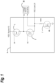
- Fig. 1 illustrates a fault tolerant solid state power controller A with two solid state switch (or FET) design where two solid state switches, solid state switch 1 and solid state switch 2 are used in series between the VDC Source 10 and the VDC Load 20.
- solid state switch 1 fails short, or closed, solid state switch 2 will block current flow when off, or open.
- solid state switch 2 fails short, solid state switch 1 may still block current flow.
- the Built-In-Tester Equipment (BITE) circuit 50 detects whether either solid state switch 1 or solid state switch 2 has failed by first activating a test gate 60 (e.g., a FET) on a small test solid state switch T to apply a small load to the Solid State Power Controller A. With all other primary state gate drives 30 and 40 in an off state, or in an open state, a voltage is applied to the input 10 and is measured at voltage sense line Va. If voltage is present, solid state switch 1 may be shorted. With solid state switch 1 on, or in a closed state, and solid state switches 2 off, or in an open state, a voltage is sensed at line Vb. If a voltage is present, solid state switch 2 may be shorted.
- a test gate 60 e.g., a FET
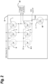
- Fig. 2 illustrates a fault tolerant Solid State Power Controller B having a four solid state switch (or FET) design in a similar configuration to the two solid state switch design of SSPC A of Fig. 1 , except that each series of two solid state switches are used in a parallel configuration. If solid state switch 1 or solid state switch 3 (similar to switches 1 and 3 in Fig. 1 ), fails short, solid state switch 2 and solid state switch 4 will block the power when off. If solid state switch 2 or solid state switch 4 fails short, solid state switch 1 and solid state switch 3 can still block current flow.
- Fig. 2 also illustrates that multiple branches of solid state switches in series, e.g., solid state switch N and solid state switch N+1, may be added in parallel between the VDC Source 10' and the VDC Load 20'.
- the Built-In-Tester Equipment (BITE) circuit 50' detects whether either solid state switches 1-4 have failed by first activating a test gate 60' on a test solid state switch T to apply a small load to the Solid State Power Controller B. With all other primary stage gate drives 20' and 30' off, i.e., open, and a voltage applied to the input, the voltage is sensed at sense line Va. If voltage is present, either solid state switch 1 or solid state switch 3 is shorted. With solid state switch 1 and solid state switch 3 on, or closed, and solid state switch 2 and solid state switch 4 off, or open, a voltage is sensed at sense line Vb. If voltage is present on Vb, one of the solid state switches 2 and 4 is shorted.
- BITE Built-In-Tester Equipment
- the controller circuit is allowed to keep functioning even though there may be a shorted solid state switch, wherein a BITE will report the shorted solid state switch failure condition to a maintenance computer or system (not shown) upon the next power up.
- MEL Minimum Equipment List
- the built-in test circuit 50/50' includes a voltage sensor between a load and at least one solid state switch.
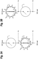
- Figs. 3A and 3B illustrates a schematic diagram of a series of solid states switches 1, 2, where one switch fails in a closed position.
- Fig. 3A illustrates a first solid state switch 1 of the plurality of solid state switches being configured to remain in an open position when a second solid state switch 2 of the plurality of solid state switches fails in a closed position.
- Fig. 3B illustrates a second solid state switch 2 of the plurality of solid state switches being configured to remain in an open position when a first solid state switch 1 of the plurality of solid state switches fails in a closed position.
- the first solid state 1 switch may be configured at its gate 20/20' (see Figs.
- the built-in test circuit further includes a solid state switch T that supplies a load to the solid state power controller A/B, and a voltage sensor Va/Vb at 50/50'between a load and at least one solid state switch.
- Fig. 4 illustrates a method of one embodiment for operating a solid state power controller where a plurality of solid state switches are provided 100 connected in series between a power source and a load, and a built-in test circuit is provided 102 that senses a voltage between at least one solid state switch of the plurality of solid state switches having one or more varying periphery sizes.
- a signal is sent 104 to each gate of the plurality of solid state switches to be in an open state. Thereafter, a load is applied 106 to the solid state power controller by a built-in test circuit.
- the method then senses 108 if an overvoltage condition across the one or more of the varying periphery sizes and opens or closes the one or more of the varying periphery sizes in accordance with a measured is present across at least one of the plurality of solid state switches to confirm that at least one of the plurality of solid states switches has failed in a closed state. Finally, a first one of the plurality of solid state switches is opened 110 when a second one of the plurality of solid state switches fails in a closed state.
- a fail-safe link including solid state switches of varying periphery sizes, e.g., gate, drain, and/or source periphery dimensionality of the solid state switches, e.g., 5 ⁇ m gate periphery, 1 mm gate periphery, 100 mm gate periphery, 10,000 mm gate periphery.
- solid state switches of varying periphery sizes, e.g., gate, drain, and/or source periphery dimensionality of the solid state switches, e.g., 5 ⁇ m gate periphery, 1 mm gate periphery, 100 mm gate periphery, 10,000 mm gate periphery.
- the fail-safe link uses a built-in test circuit that senses an overvoltage condition across one or more of the varying periphery sizes and opens or closes the one or more of the varying periphery sizes in accordance with a measured voltage across at least one solid state switch of the plurality of solid state switches.
- the fail-safe link provides a tunable, variable, and selectable thermal protection circuit, for example, that detects, for example, over voltage and over current conditions, for instance, on a mobile platform or vehicle, e.g., aircraft, so as to prevent shortening an expected usable life of a component, unlike a single, one current rating, thermal circuit breaker or the like, e.g., a 5 amp rated fuse.
Landscapes
- Physics & Mathematics (AREA)
- General Physics & Mathematics (AREA)
- Electronic Switches (AREA)
- Protection Of Static Devices (AREA)
- Power Sources (AREA)
- Logic Circuits (AREA)
- Emergency Protection Circuit Devices (AREA)
- Semiconductor Integrated Circuits (AREA)
Description
- The field of the embodiments presented herein is directed toward a solid state power controller designed to operate in a failsafe or fault tolerant state.
- The fusible link circuit breaker was developed in the early eighties to obtain wire separation relief on vehicle electronics systems. The original intent was to prevent propagation of wire damage to adjacent wires if a circuit breaker was to malfunction in a closed position and fail to open on a fault. A failure mode in older circuit breakers with silver cadmium or silver tungsten contacts was to weld together or be jammed from opening on a heavy fault current. Additionally, in a solid state power controller (SSPC), these failsafe fuses can only serve one thermal rating that causes wire integration issues by limiting the choice as to which connector or pin a load wire will come from.
- In order to gain the most wire weight savings from the application of Solid State Power Controller (SSPC) technology, a new approach to failsafe design must be devised that does not depend on a physical fusing device. Current solutions use fuses as failsafe protection for a shorted Field Effect Transistor (FET) condition. Some SSPCs do not have backup protection (the Secondary Power Distribution Assembly (SPDA) on the MMA (Multi Mission Airplane)). There exists a need to allow a circuit to keep functioning even though there may be a shorted FET, where a Built-In-Tester (BIT) will report the shorted FET failure to a maintenance computer upon the next power up. It is with respect to these and other considerations that the disclosure herein is presented.
- Document
US 2009/212975 A1 , according to its abstract, states that a switching and fault detection circuit comprises two controllable switches capable of coupling a power source to a load. A controller can control the switches and test them for faults, and a voltage sensor can read the output voltage going to the load. Dual-redundant switches and fault detection circuitry can provide correct operation if one should fail. Control and feedback logic can determine if each of the solid-state switches is operating correctly during the power-on and power-off cycles and can also check for a fail-open condition during normal operations. If it is determined that a solid switch has failed open or closed, a fault can be generated. - Document
US 6 320 405 B1 , according to its abstract, states that an apparatus for switching loads, based on a starting signal, has a first MOSFET output stage and a second downstream MOSFET output stage, each of the MOSFET output stages being controllable by a logic circuit, with a power supply voltage of the downstream MOSFET output stage being supplied over the first MOSFET output stage. The apparatus includes a line that is adapted to connect each logic circuit of the MOSFET output stages and to provide an input voltage to a logic circuit of the downstream MOSFET output stage. The apparatus also includes a monitoring arrangement, which is activated by the starting signal, that is adapted to monitor the power supply voltage of the downstream MOSFET output stage and prevent activation of the first MOSFET output stage when the power supply voltage is below a predetermined value. Also included in this apparatus is a varying arrangement that is adapted to vary the input voltage when the first MOSFET output stage is activated based on the starting signal, and an activating arrangement that is adapted to activate the downstream MOSFET output stage. The activating arrangement includes a controlling arrangement, which is connected to the line and to another line connecting the MOSFET output stages, that is adapted to control activation of the downstream MOSFET output stage and prevent activation when the power supply voltage exceeds a threshold potential and the starting signal is not detected. -
Document EP 2 124 340 A2 , according to its abstract, states that a solid state switching device (SSSD) for AC and DC high power solid state power controller includes, for DC applications, a MOSFET and an IGBT connected in parallel and an optional zener diode connecting a collector and a gate of the IGBT. For AC applications, the SSSD includes a "back to back" pair of MOSFETs connected in parallel with a pair of counterparallel IGBTs, each in series with a diode, and, optionally, zener diodes "back to back" with conventional diodes connecting a collector and a gate of each of the IGBT. A method of switching establishes a sequence of turning on/off the MOSFET(s) and the IGBT(s) wherein the IGBT(s) turn on before and turn off after the MOSFET(s). A negative feedback prevents a voltage of SSSD rising above predetermined level. - In an embodiment, a fail-safe link includes a plurality of branches connected in parallel between a power source and a load, where each of the plurality of branches contain a plurality of solid state switches of varying periphery sizes, e.g., gate, drain, or source periphery dimensionality, e.g., 5 um gate periphery, 1 mm gate periphery, 100 mm gate periphery, 10,000 mm gate periphery, ..., of the solid state switches, including field effect transistors (FETS), that are related to current or voltage handling capability, connected in series between the power source and the load, and a built-in test circuit that senses an overvoltage condition across one or more of the solid state switches having varying periphery sizes and opens or closes the one or more of the solid state switches having varying periphery sizes in accordance with a measured voltage across at least one solid state switch of the plurality of solid state switches, wherein the plurality of solid state switches comprises a plurality of Field Effect Transistors. The built-in test circuit comprises a Field Effect Transistor that supplies a load to a solid state power controller, and a voltage sensor between a load and at least one solid state switch, wherein the voltage sensor comprises a first voltage sense line and a second voltage sense line. Each branch of the plurality of branches contains two solid state switches which are a first solid state switch and a second solid state switch. Load side terminals of the first solid state switches of each branch are connected in parallel to the first voltage sense line. Load side terminals of the second solid state switches of each branch are connected in parallel to the second voltage sense line.
- In another embodiment disclosed herein, a method of operating a fail-safe link includes providing a plurality of branches connected in parallel between a power source and a load, wherein each of the plurality of branches contains a plurality of solid state switches connected in series between the power source and the load and having one or more varying periphery sizes , e.g., gate, drain, or source dimensionality, e e.g., 5 um gate periphery, 1 mm gate periphery, 100 mm gate periphery, 10,000 mm gate periphery, ... , of the solid state switches,, including field effect transistors (FETS), that are related to current or voltage handling capability, connected in series between a power source and a load, and providing a built-in test circuit that senses an overvoltage condition across one or more of the solid state switches having varying periphery sizes and opens or closes the solid state switches having one or more of the varying periphery sizes in accordance with a measured voltage across at least one solid state switch of the plurality of solid state switches. The plurality of solid state switches comprises a plurality of Field Effect Transistors. The built-in test circuit comprises a Field Effect Transistor that supplies a load to a solid state power controller, and a voltage sensor between a load and at least one solid state switch, wherein the voltage sensor comprises a first voltage sense line and a second voltage sense line. Each branch of the plurality of branches contains two solid state switches which are a first solid state switch and a second solid state switch. Load side terminals of the first solid state switches of each branch are connected in parallel to the first voltage sense line, wherein load side terminals of the second solid state switches of each branch are connected in parallel to the second voltage sense line. A first one of the plurality of solid state switches is opened when a second one of the plurality of solid state switches fails in a closed state. Thereafter, a signal is sent to each gate of the plurality of solid state switches to be in an open state, and a load is applied to the solid state power controller by a built-in test circuit. The method then senses if a voltage is present across at least one of the plurality of solid state switches to confirm that at least one of the plurality of solid state switches has failed in a closed state. For example, one or more of the fail-safe link(s) described may be utilized for a mobile vehicle application to provide variable thermal protection switchability for protection of one or more components, e.g., low noise amplifiers, high gain amplifiers, receivers, transceivers, antennas, power amplifiers, and the like as well as integrated electronics modules containing one or more components.
- The features, functions, and advantages that have been discussed can be achieved independently in various embodiments of the present disclosure or may be combined in yet other embodiments, further details of which can be seen with reference to the following description and drawings.
- The embodiments presented herein will become more fully understood from the detailed description and the accompanying drawings, wherein:
-
Fig. 1 illustrates a schematic diagram of one example not supported by the claims of a fail-safe link disclosed herein; -
Fig. 2 illustrates a schematic diagram of another embodiment of a fail-safe link disclosed herein; -
Fig. 3A illustrates a schematic diagram of a first solid state switch configured to remain in an open position when a second solid state switch fails in a closed position; -
Fig. 3B illustrates a schematic diagram of a second solid state switch configured to remain in an open position when a first solid state switch fails in a closed position; and -
Fig. 4 illustrates a method of one example for operating a fail-safe link. - Fail-safe links including solid state power controllers (SSPC) are semiconductor devices that control power (voltage and/or current) being supplied to a load. They perform supervisory and diagnostic functions in order to identify overload conditions and prevent short circuits. There are several basic types of SSPC, namely: AC controllers designed to switch alternating current (AC) voltages; DC controllers designed to switch direct current (DC) voltages; and AC/DC controllers designed to switch both AC and DC voltages. Analog controllers use variable voltage, current, or some other method of analog control. Microcontrollers require programming from external devices and are complete computer systems on a chip that typically combine an arithmetic logic unit (ALU), memory, timer/counters, serial port, input/output (I/O) ports, and a clock oscillator. SSPCs can be programmed by a computer, or by a specialized or proprietary programming method.
- Specifications for SSPC include dropout voltage, input voltage, load voltage, and maximum load current. Dropout voltage (must-release voltage, turn-off voltage) is the voltage applied to the input at or below which the output enters the OFF state. Input voltage (must operate voltage, pickup voltage, turn-on voltage) is the range of voltages which, when applied across the input terminals, maintains the ON condition across the output terminal. Load voltage (maximum switching voltage, line voltage) is the range of output supply voltages over which the SSPC normally operates. Maximum load current (maximum switching voltage range, maximum switching current) is the maximum continuous current allowed across SSPC output terminals under specified heat dissipation and ambient-temperature conditions. Other specifications for solid state power controllers (SSPC) include the number of input channels and the input current range.
- With the advance of new wide band gap semiconductors, programmability of SSPCs is now possible. Each SSPC can be programmed for different thermal ratings. As a result, the SSPC is programmed to the load on the pin that the wire designer designates to overcome wire integration problems.
- Regarding failsafe protection designs in SSPC technology, the two failure modes of an SSPC that require failsafe protection are: 1) the failure of the control circuitry to remove power from the gate of the FET, and 2) the failure of the FET itself in a shorted condition.
- In the field of avionic electrical systems, a FET gate signal has a failure rate of 5.28 X 10⁻¹⁵ per hour and the FET failure rate of 3.08 X 10⁻⁸ per hour. The probability of a hard fault on an avionic electrical wire is 2.0 X 10⁻⁷ per hour. Therefore, the probability of both events concurrently occurring is 6.16 X 10⁻¹⁵ per hour for a failed FET with a fault, and 1.056 X 10⁻²¹ per hour for a failed gate control signal circuit with a fault.
- In some cases, a shorted FET may have a high enough resistance to protect the wire until the bond wires in the SSPC fuse open. However, there is no guarantee that this occurrence will always take place. Sizing bond wires to the thermal rating of the SSPC limits the programmability of the devices and adds cost and complexity. Any physical fusing device will limit the advantage of programmability or wire weight reduction.
- Higher load ratings use multiple FETs in parallel to carry the current. If one FET shorts and the device receives an off (or open) command, all of the current of the load will be carried through the failed FET. With no fault, the load may draw current for some time through the shorted FET before burning through the bond wire. When commanded on (or close), the remaining FETs will carry more load and will decrease the Mean Time Before (MTBF) of the circuit. In this case, a Built-In Test Equipment (BITE) circuitry needs to report the failure of the FET so the circuit can be replaced at the next opportunity. If a fault occurs and a FET has failed, the burn through will be faster but is too unreliable to be counted on for failsafe operation. Lower current loads on a programmable SSPC could draw current for some time before the bond wire fuses, if ever. Another failure mode that must be considered with SSPC technology is a shorted FET that cannot be commanded off (or opened). If certain loads are commanded off, and continue to run, they may pose a safety threat. The embodiments presented herein allow the circuit to keep functioning even though there may be a shorted FET. The BITE will report the shorted FET upon the next power up.
- One of the embodiments present herein arranges solid state switches in series to form a power "AND" gate. If one FET fails closed, the second FET can open the circuit and clear a fault. This design also embodies a BITE circuit since failures must be detected so maintenance can be performed.
- Additionally, with wide band gap semiconductors, programmability is now possible. Each SSPC can be programmed for several thermal ratings. The fault tolerant design eliminates the need for failsafe fuses which can only serve one thermal rating.
- The two designs shown below are based on EPC(TM) GaN MOSFET (part number EPC2015), although any other MOSFET or solid state switch may be used. For example, each EPC FET can withstand 33A at 150°C. By putting two FETs in series, the circuit handles twice the voltage but doubles the on resistance, (see
Fig. 1 ). By adding a second series of FETs in parallel, (seeFig. 2 ), the same on resistance is achieved as a single part inFig. 1 , but now twice the load is able to e carried. De-rating the second series of FETs to 50A provides a safety margin, where this configuration may be programmable from 2.5 amps to 50 amps. This concept may carry as many parallel FETs as required for current requirements or for overload capability. - A two FET solution in parallel would be possible as the Rds (Resistance between the Drain and the Source.) for this FET is about 4 milliohms. Two FETs in series will be able to be programmed up to 25A with an Rds of 8 milliohms.
-
Fig. 1 illustrates a fault tolerant solid state power controller A with two solid state switch (or FET) design where two solid state switches,solid state switch 1 andsolid state switch 2 are used in series between theVDC Source 10 and theVDC Load 20. Whensolid state switch 1 fails short, or closed,solid state switch 2 will block current flow when off, or open. Whensolid state switch 2 fails short,solid state switch 1 may still block current flow. - The Built-In-Tester Equipment (BITE)
circuit 50 detects whether eithersolid state switch 1 orsolid state switch 2 has failed by first activating a test gate 60 (e.g., a FET) on a small test solid state switch T to apply a small load to the Solid State Power Controller A. With all other primary state gate drives 30 and 40 in an off state, or in an open state, a voltage is applied to theinput 10 and is measured at voltage sense line Va. If voltage is present,solid state switch 1 may be shorted. Withsolid state switch 1 on, or in a closed state, andsolid state switches 2 off, or in an open state, a voltage is sensed at line Vb. If a voltage is present,solid state switch 2 may be shorted. -
Fig. 2 illustrates a fault tolerant Solid State Power Controller B having a four solid state switch (or FET) design in a similar configuration to the two solid state switch design of SSPC A ofFig. 1 , except that each series of two solid state switches are used in a parallel configuration. Ifsolid state switch 1 or solid state switch 3 (similar toswitches Fig. 1 ), fails short,solid state switch 2 and solid state switch 4 will block the power when off. Ifsolid state switch 2 or solid state switch 4 fails short,solid state switch 1 andsolid state switch 3 can still block current flow.Fig. 2 also illustrates that multiple branches of solid state switches in series, e.g., solid state switch N and solid state switch N+1, may be added in parallel between the VDC Source 10' and the VDC Load 20'. - The Built-In-Tester Equipment (BITE) circuit 50' detects whether either solid state switches 1-4 have failed by first activating a test gate 60' on a test solid state switch T to apply a small load to the Solid State Power Controller B. With all other primary stage gate drives 20' and 30' off, i.e., open, and a voltage applied to the input, the voltage is sensed at sense line Va. If voltage is present, either
solid state switch 1 orsolid state switch 3 is shorted. Withsolid state switch 1 andsolid state switch 3 on, or closed, andsolid state switch 2 and solid state switch 4 off, or open, a voltage is sensed at sense line Vb. If voltage is present on Vb, one of thesolid state switches 2 and 4 is shorted. If the test shows that the SSPC B has a failed solid state switch, it can be locked out until repaired. If not on the Minimum Equipment List (MEL, the minimum equipment that must be functioning for dispatch on a revenue flight), a non-essential load may not delay dispatch. Thus, the controller circuit is allowed to keep functioning even though there may be a shorted solid state switch, wherein a BITE will report the shorted solid state switch failure condition to a maintenance computer or system (not shown) upon the next power up. - In summary, the built-in
test circuit 50/50' includes a voltage sensor between a load and at least one solid state switch.Figs. 3A and 3B illustrates a schematic diagram of a series of solid states switches 1, 2, where one switch fails in a closed position.Fig. 3A illustrates a firstsolid state switch 1 of the plurality of solid state switches being configured to remain in an open position when a secondsolid state switch 2 of the plurality of solid state switches fails in a closed position.Fig. 3B illustrates a secondsolid state switch 2 of the plurality of solid state switches being configured to remain in an open position when a firstsolid state switch 1 of the plurality of solid state switches fails in a closed position. The firstsolid state 1 switch may be configured at itsgate 20/20' (seeFigs. 1-2 ) to be in an on or closed configuration, and the secondsolid state switch 2 may be configured at itsgate 30/30' (seeFigs. 1-2 ) to be in an off or open configuration. The built-in test circuit further includes a solid state switch T that supplies a load to the solid state power controller A/B, and a voltage sensor Va/Vb at 50/50'between a load and at least one solid state switch. -
Fig. 4 illustrates a method of one embodiment for operating a solid state power controller where a plurality of solid state switches are provided 100 connected in series between a power source and a load, and a built-in test circuit is provided 102 that senses a voltage between at least one solid state switch of the plurality of solid state switches having one or more varying periphery sizes. A signal is sent 104 to each gate of the plurality of solid state switches to be in an open state. Thereafter, a load is applied 106 to the solid state power controller by a built-in test circuit. The method then senses 108 if an overvoltage condition across the one or more of the varying periphery sizes and opens or closes the one or more of the varying periphery sizes in accordance with a measured is present across at least one of the plurality of solid state switches to confirm that at least one of the plurality of solid states switches has failed in a closed state. Finally, a first one of the plurality of solid state switches is opened 110 when a second one of the plurality of solid state switches fails in a closed state. - Advantageously, a fail-safe link is disclosed including solid state switches of varying periphery sizes, e.g., gate, drain, and/or source periphery dimensionality of the solid state switches, e.g., 5 µm gate periphery, 1 mm gate periphery, 100 mm gate periphery, 10,000 mm gate periphery. These various periphery size FETS, e.g., FETS disclosed in
Figure 1 and2 , when connected in series between a power source and a load, provide improved current or voltage handling capability. The fail-safe link uses a built-in test circuit that senses an overvoltage condition across one or more of the varying periphery sizes and opens or closes the one or more of the varying periphery sizes in accordance with a measured voltage across at least one solid state switch of the plurality of solid state switches. - Advantageously, by switching in and out one or more of the varying periphery FETS, the fail-safe link provides a tunable, variable, and selectable thermal protection circuit, for example, that detects, for example, over voltage and over current conditions, for instance, on a mobile platform or vehicle, e.g., aircraft, so as to prevent shortening an expected usable life of a component, unlike a single, one current rating, thermal circuit breaker or the like, e.g., a 5 amp rated fuse.
- The subject matter described above is provided by way of illustration only and should not be construed as limiting. Various modifications and changes may be made to the subject matter described herein without following the example embodiments and applications illustrated and described, and without departing from the true scope of the present disclosure, which is set forth in the following claims.
Claims (8)
- A fail-safe link for a mobile vehicle, the fail-safe link comprising:a plurality of branches connected in parallel between a power source (10) and a load (20), where each of the plurality of branches contains a plurality of solid state switches (1, 2, 3, 4) having one or more varying periphery sizes connected in series between the power source (10) and the load (20); anda built-in test circuit (50) that is configured to sense an overvoltage condition across the one or more of the solid state switches having varying periphery sizes and to open or close the one or more of the solid state switches having varying periphery sizes in accordance with a measured voltage across at least one solid state switch of the plurality of solid state switches (1, 2, 3, 4), wherein the built-in test circuit comprises a Field Effect Transistor that is configured to supply a load to a solid state power controller, and a voltage sensor between a load and at least one solid state switch, wherein the voltage sensor comprises a first voltage sense line (Va) and a second voltage sense line (Vb),wherein the plurality of solid state switches (1, 2, 3, 4) comprises a plurality of Field Effect Transistors,wherein each branch of the plurality of branches contains two solid state switches (1, 2, 3, 4) which are a first solid state switch (1, 3) and a second solid state switch (2, 4),wherein load side terminals of the first solid state switches (1, 3) of each branch are connected in parallel to the first voltage sense line (Va), and wherein load side terminals of the second solid state switches (2, 4) of each branch are connected in parallel to the second voltage sense line (Vb).
- The fail-safe link according to claim 1, wherein the first solid state switch of the plurality of solid state switches is configured to remain in an open position when a second solid state switch of the plurality of solid state switches fails in a closed position.
- The fail-safe link according to claim 1 or 2, wherein the first and second solid state switches are configured at their gates to be in an off or open configuration.
- The fail-safe link according to any of claims 1 to 3, wherein the built-in test circuit is configured to supply a load to a solid state power controller and determine if a voltage is present across the failed second solid state switch.
- The fail-safe link according to any of claims 1 to 4, wherein the second solid state switch of the plurality of solid state switches is configured to remain in an open position when a first solid state switch of the plurality of solid state switches fails in a closed position.
- The fail-safe link according to any of claims 1 to 5, wherein, the first solid state switch being configured at its gate to be in an on or closed configuration, and the second solid state switch being configured at its gate to be in an off or open configuration.
- The fail-safe link according to any of claims 1 to 6, wherein the built-in test circuit is configured to supply a load to a solid state power controller and determine a voltage is present across the failed second solid state switch.
- A method of operating a fail-safe link for a mobile vehicle, the method comprising:providing a plurality of branches connected in parallel between a power source (10) and a load (20), where each of the plurality of branches contains a plurality of solid state switches (1, 2, 3, 4) having one or more varying periphery sizes connected in series between the power source (10) and the load (20);providing a built-in test circuit (50) that senses a voltage across at least one solid state switch of the plurality of solid state switches (1, 2, 3) having one or more varying periphery sizes, wherein the built-in test circuit comprises a Field Effect Transistor that supplies a load to a solid state power controller, and a voltage sensor between a load and at least one solid state switch, wherein the voltage sensor comprises a first voltage sense line (Va) and a second voltage sense line (Vb), wherein each branch of the plurality of branches contains two solid state switches (1, 2, 3, 4) which are a first solid state switch (1, 3) and a second solid state switch (2, 4), wherein load side terminals of the first solid state switches (1, 3) of each branch are connected in parallel to the first voltage sense line (Va), and wherein load side terminals of the second solid state switches (2, 4) of each branch are connected in parallel to the second voltage sense line (Vb);sending a signal to each gate (30, 40, 60) of the plurality of solid state switches (1, 2, 3) to be in an open state;applying a load (20) to a solid state power controller (A, B) by the built-in test circuit (50); andsensing an overvoltage condition across the one or more of the solid state switches having varying periphery sizes and opening or closing the one or more of the solid state switches having varying periphery sizes in accordance with a measured voltage across at least one of the plurality of solid state switches (1, 2, 3) to confirm that at least one of the plurality of solid states switches (1, 2, 3) has failed in a closed state; andopening a first one of the plurality of solid state switches (1, 2, 3) when a second one of the plurality of solid state switches (1, 2, 3) fails in a closed state,wherein the plurality of solid state switches (1, 2, 3, 4) comprises a plurality of Field Effect Transistors.
Applications Claiming Priority (2)
| Application Number | Priority Date | Filing Date | Title |
|---|---|---|---|
| US13/650,285 US8891218B2 (en) | 2012-10-12 | 2012-10-12 | Fault tolerant fail-safe link |
| EP13187535.3A EP2720053B1 (en) | 2012-10-12 | 2013-10-07 | Fault tolerant fail-safe link |
Related Parent Applications (2)
| Application Number | Title | Priority Date | Filing Date |
|---|---|---|---|
| EP13187535.3A Division-Into EP2720053B1 (en) | 2012-10-12 | 2013-10-07 | Fault tolerant fail-safe link |
| EP13187535.3A Division EP2720053B1 (en) | 2012-10-12 | 2013-10-07 | Fault tolerant fail-safe link |
Publications (2)
| Publication Number | Publication Date |
|---|---|
| EP3739349A1 EP3739349A1 (en) | 2020-11-18 |
| EP3739349B1 true EP3739349B1 (en) | 2023-08-16 |
Family
ID=49447926
Family Applications (2)
| Application Number | Title | Priority Date | Filing Date |
|---|---|---|---|
| EP20184384.4A Active EP3739349B1 (en) | 2012-10-12 | 2013-10-07 | Fault tolerant fail-safe link comprising parallel branches |
| EP13187535.3A Active EP2720053B1 (en) | 2012-10-12 | 2013-10-07 | Fault tolerant fail-safe link |
Family Applications After (1)
| Application Number | Title | Priority Date | Filing Date |
|---|---|---|---|
| EP13187535.3A Active EP2720053B1 (en) | 2012-10-12 | 2013-10-07 | Fault tolerant fail-safe link |
Country Status (5)
| Country | Link |
|---|---|
| US (1) | US8891218B2 (en) |
| EP (2) | EP3739349B1 (en) |
| JP (1) | JP6342135B2 (en) |
| CN (1) | CN103731121B (en) |
| BR (1) | BR102013026254B1 (en) |
Families Citing this family (21)
| Publication number | Priority date | Publication date | Assignee | Title |
|---|---|---|---|---|
| US10753979B2 (en) | 2013-04-04 | 2020-08-25 | The Boeing Company | In-situ battery monitoring system |
| JP5797809B1 (en) * | 2014-05-09 | 2015-10-21 | 三菱電機株式会社 | Electric load feeding control device |
| US9716385B2 (en) | 2014-06-16 | 2017-07-25 | Hamilton Sundstrand Corporation | Solid STTE power controller with parallel MOSFET load sharing |
| EP3176903B1 (en) * | 2015-12-04 | 2023-09-20 | HS Elektronik Systeme GmbH | Power distribution system |
| EP3176896B1 (en) * | 2015-12-04 | 2019-10-30 | HS Elektronik Systeme GmbH | Power management and distribution system |
| LU93345B1 (en) | 2016-12-08 | 2018-06-08 | Phoenix Contact Gmbh & Co Kg Intellectual Property Licenses & Standards | Protection arrangement of electrical loads and their connection lines against overcurrent |
| US10845425B2 (en) * | 2017-01-30 | 2020-11-24 | Wirepath Home Systems, Llc | Systems and methods for detecting switching circuitry failure |
| US10666042B2 (en) * | 2017-06-14 | 2020-05-26 | Hamilton Sunstrand Corporation | Elimination of secondary fuses in high power solid state power controllers |
| EP3629039B1 (en) | 2018-09-26 | 2023-04-05 | Aptiv Technologies Limited | Solid state power switch device |
| US11391805B2 (en) * | 2019-05-10 | 2022-07-19 | Hamilton Sundstrand Corporation | Systems and methods for current sense resistor built-in-test |
| US11340296B2 (en) * | 2019-06-25 | 2022-05-24 | Motorola Mobility Llc | Electronic device with solid state switch monitoring |
| US11563433B2 (en) * | 2019-10-10 | 2023-01-24 | C&C Power, Inc. | Direct current circuit switch |
| US11710960B2 (en) | 2020-09-30 | 2023-07-25 | Pony Ai Inc. | Control and operation of power distribution system |
| FR3119715B1 (en) * | 2021-02-05 | 2023-04-14 | Hager Controls | KNX or analog bus management electronic device, with electronic component protection |
| GB202215852D0 (en) * | 2022-10-26 | 2022-12-07 | Nicoventures Trading Ltd | Computing device |
| EP4609508A1 (en) * | 2022-10-26 | 2025-09-03 | Nicoventures Trading Limited | Application specific integrated circuit package and method of operating the same |
| WO2024229522A1 (en) * | 2023-05-10 | 2024-11-14 | David Stuckey Investments Pty Ltd | Time delay relay |
| DE102023117731A1 (en) * | 2023-07-05 | 2025-01-09 | WAGO Verwaltungsgesellschaft mit beschränkter Haftung | READING THE SWITCHING STATES OF TWO SWITCHES BY A MICROCONTROLLER |
| US12515812B2 (en) | 2023-09-12 | 2026-01-06 | Hamilton Sundstrand Corporation | Minimum equipment list systems for aircraft |
| GB2643375A (en) * | 2024-06-05 | 2026-02-18 | Rolls Royce Deutschland Ltd & Co Kg | A method for detecting the health of a first switching unit of a power system and power system |
| DE102025143136A1 (en) | 2024-10-22 | 2026-04-23 | Volkswagen Aktiengesellschaft | Discreetly constructed overcurrent protection device, corresponding control unit and motor vehicle with it |
Family Cites Families (33)
| Publication number | Priority date | Publication date | Assignee | Title |
|---|---|---|---|---|
| US4009420A (en) | 1975-05-02 | 1977-02-22 | The United States Of America As Represented By The Secretary Of The Navy | Solid state power controller |
| US4110809A (en) | 1976-12-30 | 1978-08-29 | Lockheed Aircraft Corporation | Solid state power controller with low level signal control |
| US4174496A (en) | 1978-08-02 | 1979-11-13 | Rockwell International Corporation | Monolithic solid state power controller |
| US4336568A (en) | 1980-07-24 | 1982-06-22 | Westinghouse Electric Corp. | Packaged solid state power controller with separable mounting for a power switching device, and method of assembly |
| US4626954A (en) | 1984-09-06 | 1986-12-02 | Eaton Corporation | Solid state power controller with overload protection |
| US4656365A (en) | 1985-07-12 | 1987-04-07 | Westinghouse Electric Corp. | Solid state power controller leakage current shunt circuit |
| US4713601A (en) | 1985-09-26 | 1987-12-15 | The Dow Chemical Company | Power proportioning controller for solid state relays |
| US4740883A (en) | 1986-08-04 | 1988-04-26 | Rockwell International Corporation | Universal solid state power controller |
| US4665355A (en) | 1986-09-15 | 1987-05-12 | Rockwell International Corporation | Off line capacitor-divider power supply for solid state power controller |
| US4724374A (en) | 1987-02-09 | 1988-02-09 | Westinghouse Electric Corp. | Solid state current limited power controller for DC circuits |
| US4864214A (en) | 1988-07-06 | 1989-09-05 | Westinghouse Electric Corp. | Solid state power controller |
| IT1227104B (en) * | 1988-09-27 | 1991-03-15 | Sgs Thomson Microelectronics | SELF-PROTECTED INTEGRATED CIRCUIT FROM POLARITY INVERSIONS OF THE POWER BATTERY |
| JPH0697793A (en) * | 1992-09-10 | 1994-04-08 | Mitsubishi Electric Corp | Circuit breaker operation control circuit |
| US5444590A (en) | 1992-12-04 | 1995-08-22 | Texas Instruments Incorporated | Solid state power controller with power switch protection apparatus |
| US5723915A (en) | 1992-12-04 | 1998-03-03 | Texas Instruments Incorporated | Solid state power controller |
| US6125024A (en) | 1993-06-03 | 2000-09-26 | Texas Instruments Incorporated | Externally programmable solid state power controller with power switch protection apparatus and method for making |
| US5752047A (en) | 1995-08-11 | 1998-05-12 | Mcdonnell Douglas Corporation | Modular solid state power controller with microcontroller |
| DE19735543A1 (en) * | 1997-08-16 | 1999-02-18 | Bosch Gmbh Robert | Load switching circuit according to input signal in car systems |
| US6108182A (en) * | 1998-10-30 | 2000-08-22 | Intersil Corporation | Overcurrent sensing circuit and self adjusting blanking |
| CA2406500C (en) * | 2001-10-01 | 2008-04-01 | Research In Motion Limited | An over-voltage protection circuit for use in a charging circuit |
| US6768350B1 (en) | 2002-04-10 | 2004-07-27 | Hamilton Sundstrand Corporation | Microprocessor based solid state DC power controller |
| US7193337B2 (en) | 2003-09-09 | 2007-03-20 | Honeywell International Inc. | System and method utilizing a solid state power controller (SSPC) for controlling an electrical load of a variable frequency three-phase power source |
| US7064448B2 (en) | 2004-09-01 | 2006-06-20 | Hamilton Sundstrand Corporation | Power controller with bond wire fuse |
| US7190124B2 (en) * | 2005-05-16 | 2007-03-13 | Lutron Electronics Co., Inc. | Two-wire dimmer with power supply and load protection circuit in the event of switch failure |
| US7505820B2 (en) | 2006-03-30 | 2009-03-17 | Honeywell International Inc. | Backup control for solid state power controller (SSPC) |
| US7626797B2 (en) | 2006-07-24 | 2009-12-01 | Hamilton Sundstrand Corporation | Solid state power controller with lightning protection |
| US7903382B2 (en) * | 2007-06-19 | 2011-03-08 | General Electric Company | MEMS micro-switch array based on current limiting enabled circuit interrupting apparatus |
| JP5123655B2 (en) | 2007-12-26 | 2013-01-23 | パナソニック株式会社 | Solid-state imaging device |
| US8148848B2 (en) | 2008-01-24 | 2012-04-03 | Honeywell International, Inc. | Solid state power controller (SSPC) used as bus tie breaker in electrical power distribution systems |
| US7973533B2 (en) * | 2008-02-27 | 2011-07-05 | Vertical Power, Inc. | In-circuit testing for integrity of solid-state switches |
| US7741883B2 (en) * | 2008-05-21 | 2010-06-22 | Honeywell International Inc. | Method of switching and switching device for solid state power controller applications |
| JP2011130077A (en) * | 2009-12-16 | 2011-06-30 | Yokogawa Electric Corp | Digital signal output circuit |
| GB2486493B (en) * | 2010-12-17 | 2016-06-15 | Ge Aviat Systems Ltd | Switching circuits and methods of testing |
-
2012
- 2012-10-12 US US13/650,285 patent/US8891218B2/en active Active
-
2013
- 2013-10-07 EP EP20184384.4A patent/EP3739349B1/en active Active
- 2013-10-07 EP EP13187535.3A patent/EP2720053B1/en active Active
- 2013-10-11 BR BR102013026254-4A patent/BR102013026254B1/en active IP Right Grant
- 2013-10-11 JP JP2013214144A patent/JP6342135B2/en active Active
- 2013-10-12 CN CN201310475609.XA patent/CN103731121B/en active Active
Also Published As
| Publication number | Publication date |
|---|---|
| JP6342135B2 (en) | 2018-06-13 |
| BR102013026254B1 (en) | 2021-10-13 |
| US8891218B2 (en) | 2014-11-18 |
| EP2720053A2 (en) | 2014-04-16 |
| EP2720053B1 (en) | 2020-08-12 |
| EP2720053A3 (en) | 2016-07-20 |
| EP3739349A1 (en) | 2020-11-18 |
| US20140103990A1 (en) | 2014-04-17 |
| BR102013026254A2 (en) | 2014-10-29 |
| JP2014112823A (en) | 2014-06-19 |
| CN103731121B (en) | 2018-04-10 |
| CN103731121A (en) | 2014-04-16 |
Similar Documents
| Publication | Publication Date | Title |
|---|---|---|
| EP3739349B1 (en) | Fault tolerant fail-safe link comprising parallel branches | |
| US11967842B2 (en) | Smart battery disconnect and protection architecture for airborne high-power modular multi-string battery pack | |
| US9197056B2 (en) | Solid state power control system for aircraft high voltage DC power distribution | |
| US8344544B2 (en) | Bus-tie SSPCS for DC power distribution system | |
| US4659942A (en) | Fault-tolerant power distribution system | |
| US7586725B2 (en) | Method of providing a secondary means of overload protection and leakage current protection in applications using solid state power controllers | |
| CN109075553B (en) | The insurance system of at least one electrical appliance for vehicle | |
| CN109314024B (en) | Distributor and safety system for a vehicle | |
| US6316956B1 (en) | Multiple redundant reliability enhancement method for integrated circuits and transistors | |
| US20170187179A1 (en) | Junction box | |
| CN111130206B (en) | Electronic circuits that provide redundant power to electrical loads | |
| EP2545626A1 (en) | Surge protection | |
| US9912226B2 (en) | Method for monitoring a battery, evaluation device, and measuring system | |
| US10686312B2 (en) | Monitoring unit for monitoring a circuit breaker comprising an electrical power supply management system and circuit breaker comprising such a unit | |
| US12597765B2 (en) | Circuit breaker unit | |
| US20250047090A1 (en) | Fuse Circuit Assembly for An Energy System and Energy System | |
| EP4601141A1 (en) | Systems and methods for protecting electrical circuits | |
| US7719809B2 (en) | Method and apparatus for distributing electrical power | |
| US20260088614A1 (en) | Power distribution system and method of using the same | |
| US20250167548A1 (en) | Aircraft electric power supply system, aircraft comprising an electric power supply system, and method of switching off the supply of electric power in an aircraft electric power supply system | |
| US20240291262A1 (en) | Overvoltage Protection Circuitry for an Electrical Device | |
| US20260088602A1 (en) | System and method for solid state power control with high reverse current | |
| US20250141202A1 (en) | Aircraft electric power supply system and aircraft comprising an electric power supply system | |
| CN121307789A (en) | End-to-end fault isolation control method and device for eVTOL low-voltage distribution boxes |
Legal Events
| Date | Code | Title | Description |
|---|---|---|---|
| PUAI | Public reference made under article 153(3) epc to a published international application that has entered the european phase |
Free format text: ORIGINAL CODE: 0009012 |
|
| STAA | Information on the status of an ep patent application or granted ep patent |
Free format text: STATUS: THE APPLICATION HAS BEEN PUBLISHED |
|
| AC | Divisional application: reference to earlier application |
Ref document number: 2720053 Country of ref document: EP Kind code of ref document: P |
|
| AK | Designated contracting states |
Kind code of ref document: A1 Designated state(s): AL AT BE BG CH CY CZ DE DK EE ES FI FR GB GR HR HU IE IS IT LI LT LU LV MC MK MT NL NO PL PT RO RS SE SI SK SM TR |
|
| STAA | Information on the status of an ep patent application or granted ep patent |
Free format text: STATUS: REQUEST FOR EXAMINATION WAS MADE |
|
| 17P | Request for examination filed |
Effective date: 20210511 |
|
| RBV | Designated contracting states (corrected) |
Designated state(s): AL AT BE BG CH CY CZ DE DK EE ES FI FR GB GR HR HU IE IS IT LI LT LU LV MC MK MT NL NO PL PT RO RS SE SI SK SM TR |
|
| STAA | Information on the status of an ep patent application or granted ep patent |
Free format text: STATUS: EXAMINATION IS IN PROGRESS |
|
| 17Q | First examination report despatched |
Effective date: 20220426 |
|
| GRAP | Despatch of communication of intention to grant a patent |
Free format text: ORIGINAL CODE: EPIDOSNIGR1 |
|
| STAA | Information on the status of an ep patent application or granted ep patent |
Free format text: STATUS: GRANT OF PATENT IS INTENDED |
|
| RAP3 | Party data changed (applicant data changed or rights of an application transferred) |
Owner name: THE BOEING COMPANY |
|
| INTG | Intention to grant announced |
Effective date: 20230317 |
|
| P01 | Opt-out of the competence of the unified patent court (upc) registered |
Effective date: 20230508 |
|
| GRAS | Grant fee paid |
Free format text: ORIGINAL CODE: EPIDOSNIGR3 |
|
| GRAA | (expected) grant |
Free format text: ORIGINAL CODE: 0009210 |
|
| STAA | Information on the status of an ep patent application or granted ep patent |
Free format text: STATUS: THE PATENT HAS BEEN GRANTED |
|
| AC | Divisional application: reference to earlier application |
Ref document number: 2720053 Country of ref document: EP Kind code of ref document: P |
|
| AK | Designated contracting states |
Kind code of ref document: B1 Designated state(s): AL AT BE BG CH CY CZ DE DK EE ES FI FR GB GR HR HU IE IS IT LI LT LU LV MC MK MT NL NO PL PT RO RS SE SI SK SM TR |
|
| REG | Reference to a national code |
Ref country code: CH Ref legal event code: EP |
|
| REG | Reference to a national code |
Ref country code: DE Ref legal event code: R096 Ref document number: 602013084475 Country of ref document: DE |
|
| REG | Reference to a national code |
Ref country code: IE Ref legal event code: FG4D |
|
| REG | Reference to a national code |
Ref country code: LT Ref legal event code: MG9D |
|
| REG | Reference to a national code |
Ref country code: NL Ref legal event code: MP Effective date: 20230816 |
|
| REG | Reference to a national code |
Ref country code: AT Ref legal event code: MK05 Ref document number: 1600570 Country of ref document: AT Kind code of ref document: T Effective date: 20230816 |
|
| PG25 | Lapsed in a contracting state [announced via postgrant information from national office to epo] |
Ref country code: GR Free format text: LAPSE BECAUSE OF FAILURE TO SUBMIT A TRANSLATION OF THE DESCRIPTION OR TO PAY THE FEE WITHIN THE PRESCRIBED TIME-LIMIT Effective date: 20231117 |
|
| PG25 | Lapsed in a contracting state [announced via postgrant information from national office to epo] |
Ref country code: IS Free format text: LAPSE BECAUSE OF FAILURE TO SUBMIT A TRANSLATION OF THE DESCRIPTION OR TO PAY THE FEE WITHIN THE PRESCRIBED TIME-LIMIT Effective date: 20231216 |
|
| PG25 | Lapsed in a contracting state [announced via postgrant information from national office to epo] |
Ref country code: SE Free format text: LAPSE BECAUSE OF FAILURE TO SUBMIT A TRANSLATION OF THE DESCRIPTION OR TO PAY THE FEE WITHIN THE PRESCRIBED TIME-LIMIT Effective date: 20230816 Ref country code: RS Free format text: LAPSE BECAUSE OF FAILURE TO SUBMIT A TRANSLATION OF THE DESCRIPTION OR TO PAY THE FEE WITHIN THE PRESCRIBED TIME-LIMIT Effective date: 20230816 Ref country code: PT Free format text: LAPSE BECAUSE OF FAILURE TO SUBMIT A TRANSLATION OF THE DESCRIPTION OR TO PAY THE FEE WITHIN THE PRESCRIBED TIME-LIMIT Effective date: 20231218 Ref country code: NO Free format text: LAPSE BECAUSE OF FAILURE TO SUBMIT A TRANSLATION OF THE DESCRIPTION OR TO PAY THE FEE WITHIN THE PRESCRIBED TIME-LIMIT Effective date: 20231116 Ref country code: NL Free format text: LAPSE BECAUSE OF FAILURE TO SUBMIT A TRANSLATION OF THE DESCRIPTION OR TO PAY THE FEE WITHIN THE PRESCRIBED TIME-LIMIT Effective date: 20230816 Ref country code: LV Free format text: LAPSE BECAUSE OF FAILURE TO SUBMIT A TRANSLATION OF THE DESCRIPTION OR TO PAY THE FEE WITHIN THE PRESCRIBED TIME-LIMIT Effective date: 20230816 Ref country code: LT Free format text: LAPSE BECAUSE OF FAILURE TO SUBMIT A TRANSLATION OF THE DESCRIPTION OR TO PAY THE FEE WITHIN THE PRESCRIBED TIME-LIMIT Effective date: 20230816 Ref country code: IS Free format text: LAPSE BECAUSE OF FAILURE TO SUBMIT A TRANSLATION OF THE DESCRIPTION OR TO PAY THE FEE WITHIN THE PRESCRIBED TIME-LIMIT Effective date: 20231216 Ref country code: HR Free format text: LAPSE BECAUSE OF FAILURE TO SUBMIT A TRANSLATION OF THE DESCRIPTION OR TO PAY THE FEE WITHIN THE PRESCRIBED TIME-LIMIT Effective date: 20230816 Ref country code: GR Free format text: LAPSE BECAUSE OF FAILURE TO SUBMIT A TRANSLATION OF THE DESCRIPTION OR TO PAY THE FEE WITHIN THE PRESCRIBED TIME-LIMIT Effective date: 20231117 Ref country code: FI Free format text: LAPSE BECAUSE OF FAILURE TO SUBMIT A TRANSLATION OF THE DESCRIPTION OR TO PAY THE FEE WITHIN THE PRESCRIBED TIME-LIMIT Effective date: 20230816 Ref country code: AT Free format text: LAPSE BECAUSE OF FAILURE TO SUBMIT A TRANSLATION OF THE DESCRIPTION OR TO PAY THE FEE WITHIN THE PRESCRIBED TIME-LIMIT Effective date: 20230816 |
|
| PG25 | Lapsed in a contracting state [announced via postgrant information from national office to epo] |
Ref country code: PL Free format text: LAPSE BECAUSE OF FAILURE TO SUBMIT A TRANSLATION OF THE DESCRIPTION OR TO PAY THE FEE WITHIN THE PRESCRIBED TIME-LIMIT Effective date: 20230816 |
|
| PG25 | Lapsed in a contracting state [announced via postgrant information from national office to epo] |
Ref country code: ES Free format text: LAPSE BECAUSE OF FAILURE TO SUBMIT A TRANSLATION OF THE DESCRIPTION OR TO PAY THE FEE WITHIN THE PRESCRIBED TIME-LIMIT Effective date: 20230816 |
|
| PG25 | Lapsed in a contracting state [announced via postgrant information from national office to epo] |
Ref country code: SM Free format text: LAPSE BECAUSE OF FAILURE TO SUBMIT A TRANSLATION OF THE DESCRIPTION OR TO PAY THE FEE WITHIN THE PRESCRIBED TIME-LIMIT Effective date: 20230816 Ref country code: RO Free format text: LAPSE BECAUSE OF FAILURE TO SUBMIT A TRANSLATION OF THE DESCRIPTION OR TO PAY THE FEE WITHIN THE PRESCRIBED TIME-LIMIT Effective date: 20230816 Ref country code: ES Free format text: LAPSE BECAUSE OF FAILURE TO SUBMIT A TRANSLATION OF THE DESCRIPTION OR TO PAY THE FEE WITHIN THE PRESCRIBED TIME-LIMIT Effective date: 20230816 Ref country code: EE Free format text: LAPSE BECAUSE OF FAILURE TO SUBMIT A TRANSLATION OF THE DESCRIPTION OR TO PAY THE FEE WITHIN THE PRESCRIBED TIME-LIMIT Effective date: 20230816 Ref country code: DK Free format text: LAPSE BECAUSE OF FAILURE TO SUBMIT A TRANSLATION OF THE DESCRIPTION OR TO PAY THE FEE WITHIN THE PRESCRIBED TIME-LIMIT Effective date: 20230816 Ref country code: CZ Free format text: LAPSE BECAUSE OF FAILURE TO SUBMIT A TRANSLATION OF THE DESCRIPTION OR TO PAY THE FEE WITHIN THE PRESCRIBED TIME-LIMIT Effective date: 20230816 Ref country code: SK Free format text: LAPSE BECAUSE OF FAILURE TO SUBMIT A TRANSLATION OF THE DESCRIPTION OR TO PAY THE FEE WITHIN THE PRESCRIBED TIME-LIMIT Effective date: 20230816 |
|
| REG | Reference to a national code |
Ref country code: DE Ref legal event code: R097 Ref document number: 602013084475 Country of ref document: DE |
|
| PG25 | Lapsed in a contracting state [announced via postgrant information from national office to epo] |
Ref country code: MC Free format text: LAPSE BECAUSE OF FAILURE TO SUBMIT A TRANSLATION OF THE DESCRIPTION OR TO PAY THE FEE WITHIN THE PRESCRIBED TIME-LIMIT Effective date: 20230816 |
|
| REG | Reference to a national code |
Ref country code: CH Ref legal event code: PL |
|
| REG | Reference to a national code |
Ref country code: BE Ref legal event code: MM Effective date: 20231031 |
|
| PG25 | Lapsed in a contracting state [announced via postgrant information from national office to epo] |
Ref country code: LU Free format text: LAPSE BECAUSE OF NON-PAYMENT OF DUE FEES Effective date: 20231007 |
|
| PLBE | No opposition filed within time limit |
Free format text: ORIGINAL CODE: 0009261 |
|
| STAA | Information on the status of an ep patent application or granted ep patent |
Free format text: STATUS: NO OPPOSITION FILED WITHIN TIME LIMIT |
|
| PG25 | Lapsed in a contracting state [announced via postgrant information from national office to epo] |
Ref country code: LU Free format text: LAPSE BECAUSE OF NON-PAYMENT OF DUE FEES Effective date: 20231007 |
|
| PG25 | Lapsed in a contracting state [announced via postgrant information from national office to epo] |
Ref country code: CH Free format text: LAPSE BECAUSE OF NON-PAYMENT OF DUE FEES Effective date: 20231031 |
|
| 26N | No opposition filed |
Effective date: 20240517 |
|
| PG25 | Lapsed in a contracting state [announced via postgrant information from national office to epo] |
Ref country code: IT Free format text: LAPSE BECAUSE OF FAILURE TO SUBMIT A TRANSLATION OF THE DESCRIPTION OR TO PAY THE FEE WITHIN THE PRESCRIBED TIME-LIMIT Effective date: 20230816 Ref country code: CH Free format text: LAPSE BECAUSE OF NON-PAYMENT OF DUE FEES Effective date: 20231031 Ref country code: SI Free format text: LAPSE BECAUSE OF FAILURE TO SUBMIT A TRANSLATION OF THE DESCRIPTION OR TO PAY THE FEE WITHIN THE PRESCRIBED TIME-LIMIT Effective date: 20230816 |
|
| PG25 | Lapsed in a contracting state [announced via postgrant information from national office to epo] |
Ref country code: BE Free format text: LAPSE BECAUSE OF NON-PAYMENT OF DUE FEES Effective date: 20231031 |
|
| PG25 | Lapsed in a contracting state [announced via postgrant information from national office to epo] |
Ref country code: IE Free format text: LAPSE BECAUSE OF NON-PAYMENT OF DUE FEES Effective date: 20231007 |
|
| PG25 | Lapsed in a contracting state [announced via postgrant information from national office to epo] |
Ref country code: IE Free format text: LAPSE BECAUSE OF NON-PAYMENT OF DUE FEES Effective date: 20231007 |
|
| PG25 | Lapsed in a contracting state [announced via postgrant information from national office to epo] |
Ref country code: BG Free format text: LAPSE BECAUSE OF FAILURE TO SUBMIT A TRANSLATION OF THE DESCRIPTION OR TO PAY THE FEE WITHIN THE PRESCRIBED TIME-LIMIT Effective date: 20230816 |
|
| PG25 | Lapsed in a contracting state [announced via postgrant information from national office to epo] |
Ref country code: BG Free format text: LAPSE BECAUSE OF FAILURE TO SUBMIT A TRANSLATION OF THE DESCRIPTION OR TO PAY THE FEE WITHIN THE PRESCRIBED TIME-LIMIT Effective date: 20230816 |
|
| PG25 | Lapsed in a contracting state [announced via postgrant information from national office to epo] |
Ref country code: CY Free format text: LAPSE BECAUSE OF FAILURE TO SUBMIT A TRANSLATION OF THE DESCRIPTION OR TO PAY THE FEE WITHIN THE PRESCRIBED TIME-LIMIT; INVALID AB INITIO Effective date: 20131007 |
|
| PG25 | Lapsed in a contracting state [announced via postgrant information from national office to epo] |
Ref country code: HU Free format text: LAPSE BECAUSE OF FAILURE TO SUBMIT A TRANSLATION OF THE DESCRIPTION OR TO PAY THE FEE WITHIN THE PRESCRIBED TIME-LIMIT; INVALID AB INITIO Effective date: 20131007 |
|
| PG25 | Lapsed in a contracting state [announced via postgrant information from national office to epo] |
Ref country code: TR Free format text: LAPSE BECAUSE OF FAILURE TO SUBMIT A TRANSLATION OF THE DESCRIPTION OR TO PAY THE FEE WITHIN THE PRESCRIBED TIME-LIMIT Effective date: 20230816 |
|
| PGFP | Annual fee paid to national office [announced via postgrant information from national office to epo] |
Ref country code: DE Payment date: 20251029 Year of fee payment: 13 |
|
| PGFP | Annual fee paid to national office [announced via postgrant information from national office to epo] |
Ref country code: GB Payment date: 20251027 Year of fee payment: 13 |
|
| PGFP | Annual fee paid to national office [announced via postgrant information from national office to epo] |
Ref country code: FR Payment date: 20251027 Year of fee payment: 13 |