EP3738762A1 - Radio wave-transmitting lustrous metal member, article using same, and method for producing same - Google Patents
Radio wave-transmitting lustrous metal member, article using same, and method for producing same Download PDFInfo
- Publication number
- EP3738762A1 EP3738762A1 EP19738662.6A EP19738662A EP3738762A1 EP 3738762 A1 EP3738762 A1 EP 3738762A1 EP 19738662 A EP19738662 A EP 19738662A EP 3738762 A1 EP3738762 A1 EP 3738762A1
- Authority
- EP
- European Patent Office
- Prior art keywords
- radio wave
- substrate
- recited
- continuous surface
- aluminum
- Prior art date
- Legal status (The legal status is an assumption and is not a legal conclusion. Google has not performed a legal analysis and makes no representation as to the accuracy of the status listed.)
- Withdrawn
Links
- 229910052751 metal Inorganic materials 0.000 title claims abstract description 125
- 239000002184 metal Substances 0.000 title claims abstract description 125
- 238000004519 manufacturing process Methods 0.000 title claims abstract description 24
- 239000000758 substrate Substances 0.000 claims abstract description 102
- 229910052782 aluminium Inorganic materials 0.000 claims abstract description 69
- XAGFODPZIPBFFR-UHFFFAOYSA-N aluminium Chemical compound [Al] XAGFODPZIPBFFR-UHFFFAOYSA-N 0.000 claims abstract description 68
- 239000000463 material Substances 0.000 claims abstract description 66
- 229910003437 indium oxide Inorganic materials 0.000 claims description 48
- PJXISJQVUVHSOJ-UHFFFAOYSA-N indium(iii) oxide Chemical compound [O-2].[O-2].[O-2].[In+3].[In+3] PJXISJQVUVHSOJ-UHFFFAOYSA-N 0.000 claims description 48
- 238000004544 sputter deposition Methods 0.000 claims description 46
- 230000005540 biological transmission Effects 0.000 claims description 42
- 239000011347 resin Substances 0.000 claims description 28
- 229920005989 resin Polymers 0.000 claims description 28
- 239000011521 glass Substances 0.000 claims description 19
- 239000004417 polycarbonate Substances 0.000 claims description 12
- 229920000515 polycarbonate Polymers 0.000 claims description 12
- 239000002932 luster Substances 0.000 claims description 10
- 229910045601 alloy Inorganic materials 0.000 claims description 8
- 239000000956 alloy Substances 0.000 claims description 7
- 238000004891 communication Methods 0.000 claims description 4
- NIXOWILDQLNWCW-UHFFFAOYSA-N acrylic acid group Chemical group C(C=C)(=O)O NIXOWILDQLNWCW-UHFFFAOYSA-N 0.000 claims description 3
- 229920000728 polyester Polymers 0.000 claims description 3
- 229920000642 polymer Polymers 0.000 claims description 3
- 229920000098 polyolefin Polymers 0.000 claims description 3
- 239000011651 chromium Substances 0.000 abstract description 25
- -1 aluminum (Al) Chemical class 0.000 abstract description 19
- VYZAMTAEIAYCRO-UHFFFAOYSA-N Chromium Chemical compound [Cr] VYZAMTAEIAYCRO-UHFFFAOYSA-N 0.000 abstract description 13
- 229910052804 chromium Inorganic materials 0.000 abstract description 13
- 229910052738 indium Inorganic materials 0.000 abstract description 13
- APFVFJFRJDLVQX-UHFFFAOYSA-N indium atom Chemical compound [In] APFVFJFRJDLVQX-UHFFFAOYSA-N 0.000 abstract description 13
- 150000002739 metals Chemical class 0.000 abstract description 10
- 239000010410 layer Substances 0.000 description 171
- 239000010408 film Substances 0.000 description 72
- 238000011156 evaluation Methods 0.000 description 35
- 230000000052 comparative effect Effects 0.000 description 22
- 239000000047 product Substances 0.000 description 21
- 229920000139 polyethylene terephthalate Polymers 0.000 description 18
- 239000005020 polyethylene terephthalate Substances 0.000 description 18
- 238000005259 measurement Methods 0.000 description 15
- XKRFYHLGVUSROY-UHFFFAOYSA-N Argon Chemical compound [Ar] XKRFYHLGVUSROY-UHFFFAOYSA-N 0.000 description 12
- 238000000034 method Methods 0.000 description 10
- XLOMVQKBTHCTTD-UHFFFAOYSA-N Zinc monoxide Chemical compound [Zn]=O XLOMVQKBTHCTTD-UHFFFAOYSA-N 0.000 description 7
- 229920003229 poly(methyl methacrylate) Polymers 0.000 description 7
- 239000004926 polymethyl methacrylate Substances 0.000 description 7
- 229910052786 argon Inorganic materials 0.000 description 6
- 239000010949 copper Substances 0.000 description 6
- 230000005684 electric field Effects 0.000 description 6
- 239000007789 gas Substances 0.000 description 6
- 238000001878 scanning electron micrograph Methods 0.000 description 6
- 239000010409 thin film Substances 0.000 description 6
- VYPSYNLAJGMNEJ-UHFFFAOYSA-N Silicium dioxide Chemical compound O=[Si]=O VYPSYNLAJGMNEJ-UHFFFAOYSA-N 0.000 description 5
- GWEVSGVZZGPLCZ-UHFFFAOYSA-N Titan oxide Chemical compound O=[Ti]=O GWEVSGVZZGPLCZ-UHFFFAOYSA-N 0.000 description 5
- 239000011248 coating agent Substances 0.000 description 5
- 238000000576 coating method Methods 0.000 description 5
- 229920000089 Cyclic olefin copolymer Polymers 0.000 description 4
- 239000004743 Polypropylene Substances 0.000 description 4
- 239000000853 adhesive Substances 0.000 description 4
- 230000001070 adhesive effect Effects 0.000 description 4
- 230000008018 melting Effects 0.000 description 4
- 238000002844 melting Methods 0.000 description 4
- 229920001155 polypropylene Polymers 0.000 description 4
- 230000008569 process Effects 0.000 description 4
- 238000001771 vacuum deposition Methods 0.000 description 4
- 229920002799 BoPET Polymers 0.000 description 3
- RYGMFSIKBFXOCR-UHFFFAOYSA-N Copper Chemical compound [Cu] RYGMFSIKBFXOCR-UHFFFAOYSA-N 0.000 description 3
- PXHVJJICTQNCMI-UHFFFAOYSA-N Nickel Chemical compound [Ni] PXHVJJICTQNCMI-UHFFFAOYSA-N 0.000 description 3
- 239000004698 Polyethylene Substances 0.000 description 3
- BQCADISMDOOEFD-UHFFFAOYSA-N Silver Chemical compound [Ag] BQCADISMDOOEFD-UHFFFAOYSA-N 0.000 description 3
- 229920000122 acrylonitrile butadiene styrene Polymers 0.000 description 3
- 239000004676 acrylonitrile butadiene styrene Substances 0.000 description 3
- 230000015572 biosynthetic process Effects 0.000 description 3
- 229910052802 copper Inorganic materials 0.000 description 3
- 238000005260 corrosion Methods 0.000 description 3
- 230000007797 corrosion Effects 0.000 description 3
- 238000000151 deposition Methods 0.000 description 3
- 238000010030 laminating Methods 0.000 description 3
- TWNQGVIAIRXVLR-UHFFFAOYSA-N oxo(oxoalumanyloxy)alumane Chemical compound O=[Al]O[Al]=O TWNQGVIAIRXVLR-UHFFFAOYSA-N 0.000 description 3
- 239000002245 particle Substances 0.000 description 3
- 229920001707 polybutylene terephthalate Polymers 0.000 description 3
- 229920000573 polyethylene Polymers 0.000 description 3
- 229910052709 silver Inorganic materials 0.000 description 3
- 239000004332 silver Substances 0.000 description 3
- JBQYATWDVHIOAR-UHFFFAOYSA-N tellanylidenegermanium Chemical compound [Te]=[Ge] JBQYATWDVHIOAR-UHFFFAOYSA-N 0.000 description 3
- 239000011787 zinc oxide Substances 0.000 description 3
- 229910000838 Al alloy Inorganic materials 0.000 description 2
- UQSXHKLRYXJYBZ-UHFFFAOYSA-N Iron oxide Chemical compound [Fe]=O UQSXHKLRYXJYBZ-UHFFFAOYSA-N 0.000 description 2
- 229930040373 Paraformaldehyde Natural products 0.000 description 2
- 239000004954 Polyphthalamide Substances 0.000 description 2
- 229910052581 Si3N4 Inorganic materials 0.000 description 2
- ATJFFYVFTNAWJD-UHFFFAOYSA-N Tin Chemical compound [Sn] ATJFFYVFTNAWJD-UHFFFAOYSA-N 0.000 description 2
- 239000005083 Zinc sulfide Substances 0.000 description 2
- 229910052681 coesite Inorganic materials 0.000 description 2
- 230000002596 correlated effect Effects 0.000 description 2
- 229910052906 cristobalite Inorganic materials 0.000 description 2
- 230000008021 deposition Effects 0.000 description 2
- 238000005516 engineering process Methods 0.000 description 2
- 239000012467 final product Substances 0.000 description 2
- AMGQUBHHOARCQH-UHFFFAOYSA-N indium;oxotin Chemical compound [In].[Sn]=O AMGQUBHHOARCQH-UHFFFAOYSA-N 0.000 description 2
- 230000007246 mechanism Effects 0.000 description 2
- 150000002736 metal compounds Chemical class 0.000 description 2
- 229920003023 plastic Polymers 0.000 description 2
- 239000004033 plastic Substances 0.000 description 2
- 239000011112 polyethylene naphthalate Substances 0.000 description 2
- 229920006324 polyoxymethylene Polymers 0.000 description 2
- 229920006375 polyphtalamide Polymers 0.000 description 2
- 229920002635 polyurethane Polymers 0.000 description 2
- 239000004814 polyurethane Substances 0.000 description 2
- 239000000377 silicon dioxide Substances 0.000 description 2
- 229910052682 stishovite Inorganic materials 0.000 description 2
- OGIDPMRJRNCKJF-UHFFFAOYSA-N titanium oxide Inorganic materials [Ti]=O OGIDPMRJRNCKJF-UHFFFAOYSA-N 0.000 description 2
- 229910052905 tridymite Inorganic materials 0.000 description 2
- 229910052984 zinc sulfide Inorganic materials 0.000 description 2
- 229910052845 zircon Inorganic materials 0.000 description 2
- 229910019714 Nb2O3 Inorganic materials 0.000 description 1
- 239000004677 Nylon Substances 0.000 description 1
- 239000004952 Polyamide Substances 0.000 description 1
- 239000004642 Polyimide Substances 0.000 description 1
- 239000004793 Polystyrene Substances 0.000 description 1
- 238000003917 TEM image Methods 0.000 description 1
- 229910009815 Ti3O5 Inorganic materials 0.000 description 1
- 229910007541 Zn O Inorganic materials 0.000 description 1
- 239000012790 adhesive layer Substances 0.000 description 1
- 239000005345 chemically strengthened glass Substances 0.000 description 1
- 230000001276 controlling effect Effects 0.000 description 1
- 229920001577 copolymer Polymers 0.000 description 1
- 230000000875 corresponding effect Effects 0.000 description 1
- 238000005034 decoration Methods 0.000 description 1
- 238000011161 development Methods 0.000 description 1
- 238000010586 diagram Methods 0.000 description 1
- 230000000694 effects Effects 0.000 description 1
- 238000010292 electrical insulation Methods 0.000 description 1
- 108010092028 endopolygalacturonase II Proteins 0.000 description 1
- 238000010438 heat treatment Methods 0.000 description 1
- 229920001519 homopolymer Polymers 0.000 description 1
- 150000002484 inorganic compounds Chemical class 0.000 description 1
- 229910010272 inorganic material Inorganic materials 0.000 description 1
- 230000003993 interaction Effects 0.000 description 1
- 238000007733 ion plating Methods 0.000 description 1
- 150000002506 iron compounds Chemical class 0.000 description 1
- JEIPFZHSYJVQDO-UHFFFAOYSA-N iron(III) oxide Inorganic materials O=[Fe]O[Fe]=O JEIPFZHSYJVQDO-UHFFFAOYSA-N 0.000 description 1
- 239000005001 laminate film Substances 0.000 description 1
- 238000001755 magnetron sputter deposition Methods 0.000 description 1
- 238000000691 measurement method Methods 0.000 description 1
- 239000007769 metal material Substances 0.000 description 1
- 229910044991 metal oxide Inorganic materials 0.000 description 1
- 150000004706 metal oxides Chemical class 0.000 description 1
- 239000000203 mixture Substances 0.000 description 1
- 238000012986 modification Methods 0.000 description 1
- 230000004048 modification Effects 0.000 description 1
- 229910052759 nickel Inorganic materials 0.000 description 1
- 150000004767 nitrides Chemical class 0.000 description 1
- 229920001778 nylon Polymers 0.000 description 1
- 230000035699 permeability Effects 0.000 description 1
- 238000005240 physical vapour deposition Methods 0.000 description 1
- 229920003207 poly(ethylene-2,6-naphthalate) Polymers 0.000 description 1
- 229920003050 poly-cycloolefin Polymers 0.000 description 1
- 229920002647 polyamide Polymers 0.000 description 1
- 229920001721 polyimide Polymers 0.000 description 1
- 229920002223 polystyrene Polymers 0.000 description 1
- 239000004800 polyvinyl chloride Substances 0.000 description 1
- 229920000915 polyvinyl chloride Polymers 0.000 description 1
- 238000012545 processing Methods 0.000 description 1
- 230000001681 protective effect Effects 0.000 description 1
- 229940065287 selenium compound Drugs 0.000 description 1
- 150000003343 selenium compounds Chemical class 0.000 description 1
- JPJALAQPGMAKDF-UHFFFAOYSA-N selenium dioxide Chemical compound O=[Se]=O JPJALAQPGMAKDF-UHFFFAOYSA-N 0.000 description 1
- 229910052710 silicon Inorganic materials 0.000 description 1
- 239000010703 silicon Substances 0.000 description 1
- 150000003377 silicon compounds Chemical class 0.000 description 1
- LIVNPJMFVYWSIS-UHFFFAOYSA-N silicon monoxide Chemical compound [Si-]#[O+] LIVNPJMFVYWSIS-UHFFFAOYSA-N 0.000 description 1
- HQVNEWCFYHHQES-UHFFFAOYSA-N silicon nitride Chemical compound N12[Si]34N5[Si]62N3[Si]51N64 HQVNEWCFYHHQES-UHFFFAOYSA-N 0.000 description 1
- 229910052814 silicon oxide Inorganic materials 0.000 description 1
- 239000002356 single layer Substances 0.000 description 1
- 239000005361 soda-lime glass Substances 0.000 description 1
- 230000003595 spectral effect Effects 0.000 description 1
- 239000000126 substance Substances 0.000 description 1
- 150000003609 titanium compounds Chemical class 0.000 description 1
- 238000007740 vapor deposition Methods 0.000 description 1
- 150000003752 zinc compounds Chemical class 0.000 description 1
- YVTHLONGBIQYBO-UHFFFAOYSA-N zinc indium(3+) oxygen(2-) Chemical compound [O--].[Zn++].[In+3] YVTHLONGBIQYBO-UHFFFAOYSA-N 0.000 description 1
- DRDVZXDWVBGGMH-UHFFFAOYSA-N zinc;sulfide Chemical compound [S-2].[Zn+2] DRDVZXDWVBGGMH-UHFFFAOYSA-N 0.000 description 1
- GFQYVLUOOAAOGM-UHFFFAOYSA-N zirconium(iv) silicate Chemical compound [Zr+4].[O-][Si]([O-])([O-])[O-] GFQYVLUOOAAOGM-UHFFFAOYSA-N 0.000 description 1
Images


Classifications
-
- B—PERFORMING OPERATIONS; TRANSPORTING
- B32—LAYERED PRODUCTS
- B32B—LAYERED PRODUCTS, i.e. PRODUCTS BUILT-UP OF STRATA OF FLAT OR NON-FLAT, e.g. CELLULAR OR HONEYCOMB, FORM
- B32B15/00—Layered products comprising a layer of metal
- B32B15/20—Layered products comprising a layer of metal comprising aluminium or copper
-
- C—CHEMISTRY; METALLURGY
- C03—GLASS; MINERAL OR SLAG WOOL
- C03C—CHEMICAL COMPOSITION OF GLASSES, GLAZES OR VITREOUS ENAMELS; SURFACE TREATMENT OF GLASS; SURFACE TREATMENT OF FIBRES OR FILAMENTS MADE FROM GLASS, MINERALS OR SLAGS; JOINING GLASS TO GLASS OR OTHER MATERIALS
- C03C17/00—Surface treatment of glass, not in the form of fibres or filaments, by coating
- C03C17/44—Lustring
-
- B—PERFORMING OPERATIONS; TRANSPORTING
- B32—LAYERED PRODUCTS
- B32B—LAYERED PRODUCTS, i.e. PRODUCTS BUILT-UP OF STRATA OF FLAT OR NON-FLAT, e.g. CELLULAR OR HONEYCOMB, FORM
- B32B15/00—Layered products comprising a layer of metal
- B32B15/04—Layered products comprising a layer of metal comprising metal as the main or only constituent of a layer, which is next to another layer of the same or of a different material
- B32B15/08—Layered products comprising a layer of metal comprising metal as the main or only constituent of a layer, which is next to another layer of the same or of a different material of synthetic resin
- B32B15/09—Layered products comprising a layer of metal comprising metal as the main or only constituent of a layer, which is next to another layer of the same or of a different material of synthetic resin comprising polyesters
-
- B—PERFORMING OPERATIONS; TRANSPORTING
- B32—LAYERED PRODUCTS
- B32B—LAYERED PRODUCTS, i.e. PRODUCTS BUILT-UP OF STRATA OF FLAT OR NON-FLAT, e.g. CELLULAR OR HONEYCOMB, FORM
- B32B17/00—Layered products essentially comprising sheet glass, or glass, slag, or like fibres
- B32B17/06—Layered products essentially comprising sheet glass, or glass, slag, or like fibres comprising glass as the main or only constituent of a layer, next to another layer of a specific material
-
- B—PERFORMING OPERATIONS; TRANSPORTING
- B32—LAYERED PRODUCTS
- B32B—LAYERED PRODUCTS, i.e. PRODUCTS BUILT-UP OF STRATA OF FLAT OR NON-FLAT, e.g. CELLULAR OR HONEYCOMB, FORM
- B32B17/00—Layered products essentially comprising sheet glass, or glass, slag, or like fibres
- B32B17/06—Layered products essentially comprising sheet glass, or glass, slag, or like fibres comprising glass as the main or only constituent of a layer, next to another layer of a specific material
- B32B17/061—Layered products essentially comprising sheet glass, or glass, slag, or like fibres comprising glass as the main or only constituent of a layer, next to another layer of a specific material of metal
-
- B—PERFORMING OPERATIONS; TRANSPORTING
- B32—LAYERED PRODUCTS
- B32B—LAYERED PRODUCTS, i.e. PRODUCTS BUILT-UP OF STRATA OF FLAT OR NON-FLAT, e.g. CELLULAR OR HONEYCOMB, FORM
- B32B27/00—Layered products comprising a layer of synthetic resin
- B32B27/06—Layered products comprising a layer of synthetic resin as the main or only constituent of a layer, which is next to another layer of the same or of a different material
-
- B—PERFORMING OPERATIONS; TRANSPORTING
- B32—LAYERED PRODUCTS
- B32B—LAYERED PRODUCTS, i.e. PRODUCTS BUILT-UP OF STRATA OF FLAT OR NON-FLAT, e.g. CELLULAR OR HONEYCOMB, FORM
- B32B27/00—Layered products comprising a layer of synthetic resin
- B32B27/18—Layered products comprising a layer of synthetic resin characterised by the use of special additives
-
- B—PERFORMING OPERATIONS; TRANSPORTING
- B32—LAYERED PRODUCTS
- B32B—LAYERED PRODUCTS, i.e. PRODUCTS BUILT-UP OF STRATA OF FLAT OR NON-FLAT, e.g. CELLULAR OR HONEYCOMB, FORM
- B32B27/00—Layered products comprising a layer of synthetic resin
- B32B27/30—Layered products comprising a layer of synthetic resin comprising vinyl (co)polymers; comprising acrylic (co)polymers
- B32B27/308—Layered products comprising a layer of synthetic resin comprising vinyl (co)polymers; comprising acrylic (co)polymers comprising acrylic (co)polymers
-
- B—PERFORMING OPERATIONS; TRANSPORTING
- B32—LAYERED PRODUCTS
- B32B—LAYERED PRODUCTS, i.e. PRODUCTS BUILT-UP OF STRATA OF FLAT OR NON-FLAT, e.g. CELLULAR OR HONEYCOMB, FORM
- B32B27/00—Layered products comprising a layer of synthetic resin
- B32B27/32—Layered products comprising a layer of synthetic resin comprising polyolefins
-
- B—PERFORMING OPERATIONS; TRANSPORTING
- B32—LAYERED PRODUCTS
- B32B—LAYERED PRODUCTS, i.e. PRODUCTS BUILT-UP OF STRATA OF FLAT OR NON-FLAT, e.g. CELLULAR OR HONEYCOMB, FORM
- B32B27/00—Layered products comprising a layer of synthetic resin
- B32B27/36—Layered products comprising a layer of synthetic resin comprising polyesters
- B32B27/365—Layered products comprising a layer of synthetic resin comprising polyesters comprising polycarbonates
-
- B—PERFORMING OPERATIONS; TRANSPORTING
- B32—LAYERED PRODUCTS
- B32B—LAYERED PRODUCTS, i.e. PRODUCTS BUILT-UP OF STRATA OF FLAT OR NON-FLAT, e.g. CELLULAR OR HONEYCOMB, FORM
- B32B3/00—Layered products comprising a layer with external or internal discontinuities or unevennesses, or a layer of non-planar shape; Layered products comprising a layer having particular features of form
- B32B3/10—Layered products comprising a layer with external or internal discontinuities or unevennesses, or a layer of non-planar shape; Layered products comprising a layer having particular features of form characterised by a discontinuous layer, i.e. formed of separate pieces of material
- B32B3/14—Layered products comprising a layer with external or internal discontinuities or unevennesses, or a layer of non-planar shape; Layered products comprising a layer having particular features of form characterised by a discontinuous layer, i.e. formed of separate pieces of material characterised by a face layer formed of separate pieces of material which are juxtaposed side-by-side
-
- B—PERFORMING OPERATIONS; TRANSPORTING
- B32—LAYERED PRODUCTS
- B32B—LAYERED PRODUCTS, i.e. PRODUCTS BUILT-UP OF STRATA OF FLAT OR NON-FLAT, e.g. CELLULAR OR HONEYCOMB, FORM
- B32B9/00—Layered products comprising a layer of a particular substance not covered by groups B32B11/00 - B32B29/00
- B32B9/005—Layered products comprising a layer of a particular substance not covered by groups B32B11/00 - B32B29/00 comprising one layer of ceramic material, e.g. porcelain, ceramic tile
-
- C—CHEMISTRY; METALLURGY
- C03—GLASS; MINERAL OR SLAG WOOL
- C03C—CHEMICAL COMPOSITION OF GLASSES, GLAZES OR VITREOUS ENAMELS; SURFACE TREATMENT OF GLASS; SURFACE TREATMENT OF FIBRES OR FILAMENTS MADE FROM GLASS, MINERALS OR SLAGS; JOINING GLASS TO GLASS OR OTHER MATERIALS
- C03C17/00—Surface treatment of glass, not in the form of fibres or filaments, by coating
- C03C17/06—Surface treatment of glass, not in the form of fibres or filaments, by coating with metals
- C03C17/09—Surface treatment of glass, not in the form of fibres or filaments, by coating with metals by deposition from the vapour phase
-
- C—CHEMISTRY; METALLURGY
- C03—GLASS; MINERAL OR SLAG WOOL
- C03C—CHEMICAL COMPOSITION OF GLASSES, GLAZES OR VITREOUS ENAMELS; SURFACE TREATMENT OF GLASS; SURFACE TREATMENT OF FIBRES OR FILAMENTS MADE FROM GLASS, MINERALS OR SLAGS; JOINING GLASS TO GLASS OR OTHER MATERIALS
- C03C17/00—Surface treatment of glass, not in the form of fibres or filaments, by coating
- C03C17/34—Surface treatment of glass, not in the form of fibres or filaments, by coating with at least two coatings having different compositions
- C03C17/36—Surface treatment of glass, not in the form of fibres or filaments, by coating with at least two coatings having different compositions at least one coating being a metal
-
- C—CHEMISTRY; METALLURGY
- C03—GLASS; MINERAL OR SLAG WOOL
- C03C—CHEMICAL COMPOSITION OF GLASSES, GLAZES OR VITREOUS ENAMELS; SURFACE TREATMENT OF GLASS; SURFACE TREATMENT OF FIBRES OR FILAMENTS MADE FROM GLASS, MINERALS OR SLAGS; JOINING GLASS TO GLASS OR OTHER MATERIALS
- C03C17/00—Surface treatment of glass, not in the form of fibres or filaments, by coating
- C03C17/34—Surface treatment of glass, not in the form of fibres or filaments, by coating with at least two coatings having different compositions
- C03C17/36—Surface treatment of glass, not in the form of fibres or filaments, by coating with at least two coatings having different compositions at least one coating being a metal
- C03C17/3602—Surface treatment of glass, not in the form of fibres or filaments, by coating with at least two coatings having different compositions at least one coating being a metal the metal being present as a layer
- C03C17/3649—Surface treatment of glass, not in the form of fibres or filaments, by coating with at least two coatings having different compositions at least one coating being a metal the metal being present as a layer made of metals other than silver
-
- C—CHEMISTRY; METALLURGY
- C03—GLASS; MINERAL OR SLAG WOOL
- C03C—CHEMICAL COMPOSITION OF GLASSES, GLAZES OR VITREOUS ENAMELS; SURFACE TREATMENT OF GLASS; SURFACE TREATMENT OF FIBRES OR FILAMENTS MADE FROM GLASS, MINERALS OR SLAGS; JOINING GLASS TO GLASS OR OTHER MATERIALS
- C03C17/00—Surface treatment of glass, not in the form of fibres or filaments, by coating
- C03C17/34—Surface treatment of glass, not in the form of fibres or filaments, by coating with at least two coatings having different compositions
- C03C17/36—Surface treatment of glass, not in the form of fibres or filaments, by coating with at least two coatings having different compositions at least one coating being a metal
- C03C17/3602—Surface treatment of glass, not in the form of fibres or filaments, by coating with at least two coatings having different compositions at least one coating being a metal the metal being present as a layer
- C03C17/3668—Surface treatment of glass, not in the form of fibres or filaments, by coating with at least two coatings having different compositions at least one coating being a metal the metal being present as a layer the multilayer coating having electrical properties
-
- C—CHEMISTRY; METALLURGY
- C23—COATING METALLIC MATERIAL; COATING MATERIAL WITH METALLIC MATERIAL; CHEMICAL SURFACE TREATMENT; DIFFUSION TREATMENT OF METALLIC MATERIAL; COATING BY VACUUM EVAPORATION, BY SPUTTERING, BY ION IMPLANTATION OR BY CHEMICAL VAPOUR DEPOSITION, IN GENERAL; INHIBITING CORROSION OF METALLIC MATERIAL OR INCRUSTATION IN GENERAL
- C23C—COATING METALLIC MATERIAL; COATING MATERIAL WITH METALLIC MATERIAL; SURFACE TREATMENT OF METALLIC MATERIAL BY DIFFUSION INTO THE SURFACE, BY CHEMICAL CONVERSION OR SUBSTITUTION; COATING BY VACUUM EVAPORATION, BY SPUTTERING, BY ION IMPLANTATION OR BY CHEMICAL VAPOUR DEPOSITION, IN GENERAL
- C23C14/00—Coating by vacuum evaporation, by sputtering or by ion implantation of the coating forming material
- C23C14/04—Coating on selected surface areas, e.g. using masks
-
- C—CHEMISTRY; METALLURGY
- C23—COATING METALLIC MATERIAL; COATING MATERIAL WITH METALLIC MATERIAL; CHEMICAL SURFACE TREATMENT; DIFFUSION TREATMENT OF METALLIC MATERIAL; COATING BY VACUUM EVAPORATION, BY SPUTTERING, BY ION IMPLANTATION OR BY CHEMICAL VAPOUR DEPOSITION, IN GENERAL; INHIBITING CORROSION OF METALLIC MATERIAL OR INCRUSTATION IN GENERAL
- C23C—COATING METALLIC MATERIAL; COATING MATERIAL WITH METALLIC MATERIAL; SURFACE TREATMENT OF METALLIC MATERIAL BY DIFFUSION INTO THE SURFACE, BY CHEMICAL CONVERSION OR SUBSTITUTION; COATING BY VACUUM EVAPORATION, BY SPUTTERING, BY ION IMPLANTATION OR BY CHEMICAL VAPOUR DEPOSITION, IN GENERAL
- C23C14/00—Coating by vacuum evaporation, by sputtering or by ion implantation of the coating forming material
- C23C14/06—Coating by vacuum evaporation, by sputtering or by ion implantation of the coating forming material characterised by the coating material
- C23C14/08—Oxides
-
- C—CHEMISTRY; METALLURGY
- C23—COATING METALLIC MATERIAL; COATING MATERIAL WITH METALLIC MATERIAL; CHEMICAL SURFACE TREATMENT; DIFFUSION TREATMENT OF METALLIC MATERIAL; COATING BY VACUUM EVAPORATION, BY SPUTTERING, BY ION IMPLANTATION OR BY CHEMICAL VAPOUR DEPOSITION, IN GENERAL; INHIBITING CORROSION OF METALLIC MATERIAL OR INCRUSTATION IN GENERAL
- C23C—COATING METALLIC MATERIAL; COATING MATERIAL WITH METALLIC MATERIAL; SURFACE TREATMENT OF METALLIC MATERIAL BY DIFFUSION INTO THE SURFACE, BY CHEMICAL CONVERSION OR SUBSTITUTION; COATING BY VACUUM EVAPORATION, BY SPUTTERING, BY ION IMPLANTATION OR BY CHEMICAL VAPOUR DEPOSITION, IN GENERAL
- C23C14/00—Coating by vacuum evaporation, by sputtering or by ion implantation of the coating forming material
- C23C14/06—Coating by vacuum evaporation, by sputtering or by ion implantation of the coating forming material characterised by the coating material
- C23C14/08—Oxides
- C23C14/086—Oxides of zinc, germanium, cadmium, indium, tin, thallium or bismuth
-
- C—CHEMISTRY; METALLURGY
- C23—COATING METALLIC MATERIAL; COATING MATERIAL WITH METALLIC MATERIAL; CHEMICAL SURFACE TREATMENT; DIFFUSION TREATMENT OF METALLIC MATERIAL; COATING BY VACUUM EVAPORATION, BY SPUTTERING, BY ION IMPLANTATION OR BY CHEMICAL VAPOUR DEPOSITION, IN GENERAL; INHIBITING CORROSION OF METALLIC MATERIAL OR INCRUSTATION IN GENERAL
- C23C—COATING METALLIC MATERIAL; COATING MATERIAL WITH METALLIC MATERIAL; SURFACE TREATMENT OF METALLIC MATERIAL BY DIFFUSION INTO THE SURFACE, BY CHEMICAL CONVERSION OR SUBSTITUTION; COATING BY VACUUM EVAPORATION, BY SPUTTERING, BY ION IMPLANTATION OR BY CHEMICAL VAPOUR DEPOSITION, IN GENERAL
- C23C14/00—Coating by vacuum evaporation, by sputtering or by ion implantation of the coating forming material
- C23C14/06—Coating by vacuum evaporation, by sputtering or by ion implantation of the coating forming material characterised by the coating material
- C23C14/14—Metallic material, boron or silicon
-
- B—PERFORMING OPERATIONS; TRANSPORTING
- B32—LAYERED PRODUCTS
- B32B—LAYERED PRODUCTS, i.e. PRODUCTS BUILT-UP OF STRATA OF FLAT OR NON-FLAT, e.g. CELLULAR OR HONEYCOMB, FORM
- B32B2250/00—Layers arrangement
- B32B2250/02—2 layers
-
- B—PERFORMING OPERATIONS; TRANSPORTING
- B32—LAYERED PRODUCTS
- B32B—LAYERED PRODUCTS, i.e. PRODUCTS BUILT-UP OF STRATA OF FLAT OR NON-FLAT, e.g. CELLULAR OR HONEYCOMB, FORM
- B32B2250/00—Layers arrangement
- B32B2250/03—3 layers
-
- B—PERFORMING OPERATIONS; TRANSPORTING
- B32—LAYERED PRODUCTS
- B32B—LAYERED PRODUCTS, i.e. PRODUCTS BUILT-UP OF STRATA OF FLAT OR NON-FLAT, e.g. CELLULAR OR HONEYCOMB, FORM
- B32B2250/00—Layers arrangement
- B32B2250/44—Number of layers variable across the laminate
-
- B—PERFORMING OPERATIONS; TRANSPORTING
- B32—LAYERED PRODUCTS
- B32B—LAYERED PRODUCTS, i.e. PRODUCTS BUILT-UP OF STRATA OF FLAT OR NON-FLAT, e.g. CELLULAR OR HONEYCOMB, FORM
- B32B2307/00—Properties of the layers or laminate
- B32B2307/70—Other properties
-
- B—PERFORMING OPERATIONS; TRANSPORTING
- B32—LAYERED PRODUCTS
- B32B—LAYERED PRODUCTS, i.e. PRODUCTS BUILT-UP OF STRATA OF FLAT OR NON-FLAT, e.g. CELLULAR OR HONEYCOMB, FORM
- B32B2311/00—Metals, their alloys or their compounds
- B32B2311/24—Aluminium
-
- B—PERFORMING OPERATIONS; TRANSPORTING
- B32—LAYERED PRODUCTS
- B32B—LAYERED PRODUCTS, i.e. PRODUCTS BUILT-UP OF STRATA OF FLAT OR NON-FLAT, e.g. CELLULAR OR HONEYCOMB, FORM
- B32B2315/00—Other materials containing non-metallic inorganic compounds not provided for in groups B32B2311/00 - B32B2313/04
- B32B2315/08—Glass
-
- B—PERFORMING OPERATIONS; TRANSPORTING
- B32—LAYERED PRODUCTS
- B32B—LAYERED PRODUCTS, i.e. PRODUCTS BUILT-UP OF STRATA OF FLAT OR NON-FLAT, e.g. CELLULAR OR HONEYCOMB, FORM
- B32B2323/00—Polyalkenes
-
- B—PERFORMING OPERATIONS; TRANSPORTING
- B32—LAYERED PRODUCTS
- B32B—LAYERED PRODUCTS, i.e. PRODUCTS BUILT-UP OF STRATA OF FLAT OR NON-FLAT, e.g. CELLULAR OR HONEYCOMB, FORM
- B32B2367/00—Polyesters, e.g. PET, i.e. polyethylene terephthalate
-
- B—PERFORMING OPERATIONS; TRANSPORTING
- B32—LAYERED PRODUCTS
- B32B—LAYERED PRODUCTS, i.e. PRODUCTS BUILT-UP OF STRATA OF FLAT OR NON-FLAT, e.g. CELLULAR OR HONEYCOMB, FORM
- B32B2369/00—Polycarbonates
-
- C—CHEMISTRY; METALLURGY
- C03—GLASS; MINERAL OR SLAG WOOL
- C03C—CHEMICAL COMPOSITION OF GLASSES, GLAZES OR VITREOUS ENAMELS; SURFACE TREATMENT OF GLASS; SURFACE TREATMENT OF FIBRES OR FILAMENTS MADE FROM GLASS, MINERALS OR SLAGS; JOINING GLASS TO GLASS OR OTHER MATERIALS
- C03C2217/00—Coatings on glass
- C03C2217/20—Materials for coating a single layer on glass
- C03C2217/25—Metals
- C03C2217/251—Al, Cu, Mg or noble metals
- C03C2217/252—Al
-
- C—CHEMISTRY; METALLURGY
- C03—GLASS; MINERAL OR SLAG WOOL
- C03C—CHEMICAL COMPOSITION OF GLASSES, GLAZES OR VITREOUS ENAMELS; SURFACE TREATMENT OF GLASS; SURFACE TREATMENT OF FIBRES OR FILAMENTS MADE FROM GLASS, MINERALS OR SLAGS; JOINING GLASS TO GLASS OR OTHER MATERIALS
- C03C2217/00—Coatings on glass
- C03C2217/20—Materials for coating a single layer on glass
- C03C2217/25—Metals
- C03C2217/27—Mixtures of metals, alloys
-
- C—CHEMISTRY; METALLURGY
- C03—GLASS; MINERAL OR SLAG WOOL
- C03C—CHEMICAL COMPOSITION OF GLASSES, GLAZES OR VITREOUS ENAMELS; SURFACE TREATMENT OF GLASS; SURFACE TREATMENT OF FIBRES OR FILAMENTS MADE FROM GLASS, MINERALS OR SLAGS; JOINING GLASS TO GLASS OR OTHER MATERIALS
- C03C2217/00—Coatings on glass
- C03C2217/90—Other aspects of coatings
- C03C2217/94—Transparent conductive oxide layers [TCO] being part of a multilayer coating
- C03C2217/948—Layers comprising indium tin oxide [ITO]
-
- C—CHEMISTRY; METALLURGY
- C03—GLASS; MINERAL OR SLAG WOOL
- C03C—CHEMICAL COMPOSITION OF GLASSES, GLAZES OR VITREOUS ENAMELS; SURFACE TREATMENT OF GLASS; SURFACE TREATMENT OF FIBRES OR FILAMENTS MADE FROM GLASS, MINERALS OR SLAGS; JOINING GLASS TO GLASS OR OTHER MATERIALS
- C03C2218/00—Methods for coating glass
- C03C2218/10—Deposition methods
- C03C2218/15—Deposition methods from the vapour phase
- C03C2218/154—Deposition methods from the vapour phase by sputtering
Definitions
- the present invention relates to a metallic lustrous member with radio wave transmissibility, an article using the member, and a production method for the member or the article.
- a metallic lustrous member having both lustrousness and radio wave transmissibility (permeability) is needed, for example, to decorate a cover member of a millimeter-wave radar mounted to a front component such as a front grille or an emblem at a front end of an automotive vehicle.
- the millimeter-wave radar is configured to transmit an electromagnetic wave having a millimeter waveband (frequency: about 77 GHz, wavelength: about 4 mm) forwardly with respect to the vehicle, and receive and analyze a reflected wave from a target so as to measure a distance or a direction with respect to the target, or the size of the target.
- a result of the measurement can be utilized for inter-vehicle distance measurement, automatic vehicle speed adjustment, automatic brake adjustment, etc.
- the front component of the vehicle to which the millimeter-wave radar is mounted is a portion constituting, so to say, the face of the vehicle, and giving a profound impression on a user. Thus, it is preferable to create a high-class appearance or the like by a metallic lustrous front decoration.
- the front component of the vehicle is made of a metal material, it will substantially preclude or hinder the millimeter-wave radar from emitting and receiving an electromagnetic wave. Therefore, in order to prevent hindering of the function of the millimeter-wave radar without spoiling an aesthetic appearance of the vehicle, there is a need for a metallic lustrous member having both lustrousness and radio wave transmissibility.
- this type of metallic lustrous member is expected to be applied to various other devices requiring signal transmitting-receiving, e.g., a door handle module of an automotive vehicle using a smart key system, in-vehicle communication devices, and electronic devices such as a mobile phone and a personal computer. Further, in recent years, along with development in IoT technologies, the metallic lustrous member is also expected to be applied to a wide range of fields, e.g., home or daily-life appliances such as a refrigerator, in which signal transmitting-receiving has heretofore not been performed.
- Patent Document 1 there is disclosed a resin product comprising a metal coating or film made of chromium (Cr) or indium (In).
- This resin product comprises: a resin substrate; an inorganic underlying film (inorganic undercoating) containing an inorganic compound and formed on the resin substrate; and the metal film made of chromium (Cr) or indium (In), wherein the metal film is formed on the inorganic underlying film by a physical vapor deposition process to have a lustrous and discontinuous structure.
- the inorganic underlying film is composed of (a) a thin film of a metal compound such as: a titanium compound including titanium oxide (TiO, TiO 2 , Ti 3 O 5 , etc.); a silicon compound including silicon oxide (SiO, SiO 2 , etc.) or silicon nitride (Si 3 N 4 , etc.); an aluminum compound including aluminum oxide (Al 2 O 3 ); an iron compound including iron oxide (Fe 2 O 3 ); a selenium compound including selenium oxide (CeO); a zircon compound including zircon oxide (ZrO); or a zinc compound including zinc sulfide (ZnS), or (b) a coating film made of an inorganic coating material, e.g., a coating film made of an inorganic coating material comprising a primary component consisting of silicon, amorphousTiO 2 or the like (additionally, any of the metal compounds exemplified above).
- a metal compound such as: a titanium compound
- this resin product is based on the assumption of using only chromium (Cr) or indium (In) as a material for the metal film.
- a metal superior to chromium and indium in terms of cost and lustrousness, such as aluminum (Al) cannot be used as a material for the metal film.
- Patent Document 2 there is disclosed a lustrous resin product with electromagnetic wave transmissibility, comprising a metal film which may be formed of not only chromium (Cr) or indium (In) but also aluminum (Al), silver (Ag) or nickel (Ni).
- a metal film which may be formed of not only chromium (Cr) or indium (In) but also aluminum (Al), silver (Ag) or nickel (Ni).
- an underlying film having a discontinuous structure is provided, and then the metal film is formed on each of a plurality of discontinuous portions of the underlying film.
- an inclination angle of a substrate during sputtering must be set to 0° or 70° to form the underlying film in a discontinuous layer, there is a problem of complexity in production process.
- it is impossible to form the metal film using zinc (Zn), lead (Pb) or copper (Cu), or an alloy thereof.
- the present invention has been made to solve the above conventional problems, and an object thereof is to provide a metallic lustrous member with radio wave transmissibility, which is capable of being easily produced, wherein not only chromium (Cr) or indium (In) but also any of some other metals such as aluminum (Al) is formed as a metal layer on a continuous surface of any of various materials, and an article using the member. It is another object of the present invention to provide a production method for a metallic lustrous member with radio wave transmissibility, or an article using the member, which is capable of easily forming, as a metal layer, not only chromium (Cr) or indium (In) but also any of some other metals such as aluminum (Al), on a continuous surface of any of various materials.
- the present inventors found that, by using AC (alternating current) sputtering, it becomes possible to cause a metal which normally has difficulty in being formed into a discontinuous structure, such as aluminum (Al), to develop a discontinuous structure on a continuous surface of any of various materials, and have reached accomplishment of the present invention.
- AC alternating current
- a metallic lustrous member with radio wave transmissibility which comprises: a substrate having radio wave transmissibility; and an aluminum layer formed directly on a continuous surface of the substrate, wherein the aluminum layer has a discontinuous region including a plurality of separated segments which are mutually discontinuous.
- the metallic lustrous member according to the first aspect of the present invention is capable of being easily produced, while ensuring a structure in which not only chromium (Cr) or indium (In) but also any of some other metals such as aluminum (Al) is formed as a metal layer on a continuous surface of any of various materials.
- the aluminum layer has a sheet resistance of 90 ⁇ / ⁇ or more.
- a metallic lustrous member with radio wave transmissibility which comprises: a substrate having radio wave transmissibility; and an aluminum layer formed directly on a continuous surface of the substrate, wherein the member has a sheet resistance of 90 ⁇ / ⁇ or more.
- the metallic lustrous member according to the second aspect of the present invention is capable of being easily produced, while ensuring a structure in which not only chromium (Cr) or indium (In) but also any of some other metals such as aluminum (Al) is formed as a metal layer on a continuous surface of any of various materials.
- the continuous surface may be formed of a dielectric resin material or a glass material.
- the dielectric resin material may be comprised of any one of polyester, polyolefin, acrylic-based polymer, and polycarbonate.
- the continuous surface may be formed using an indium oxide-containing material.
- the substrate may be one selected from the group consisting of a film, a resin molded product, a glass product, and an article itself to be imparted with metallic luster.
- the aluminum layer has a maximum thickness of 15 to 80 nm.
- the aluminum layer has a radio wave transmission attenuation amount of 10 dB or less.
- the aluminum layer may be one of aluminum (Al) and an aluminum (Al) alloy.
- a content ratio of aluminum to an entire metal component in the aluminum (Al) alloy is preferably 50% or more.
- the aluminum layer may be provided on an inner surface of a transparent housing formed using the continuous surface of the substrate.
- a production method for a metallic lustrous member with radio wave transmissibility, or an article using the member comprises the step of forming an aluminum layer directly on a substrate having radio wave transmissibility by means of AC sputtering, wherein the aluminum layer has a discontinuous region including a plurality of separated segments which are mutually discontinuous.
- a production method for a metallic lustrous member with radio wave transmissibility, or an article using the member comprises the step of forming an aluminum layer directly on a substrate having radio wave transmissibility by means of AC sputtering, such that the aluminum layer has a sheet resistance of 90 ⁇ / ⁇ or more
- the production method according to the third or fourth aspect of the present invention makes it possible to easily form, as a metal layer, not only chromium (Cr) or indium (In) but also any of some other metals such as aluminum (Al), on a continuous surface of any of various materials.
- the aluminum layer may be formed directly on a continuous surface of the substrate.
- the continuous surface may be formed of a dielectric resin material or a glass material, or may be formed using an indium oxide-containing material.
- the AC sputtering is performed under a pressure of 1.5 Pa or more.
- the substrate has a temperature of 20°C or more.
- the present invention provides: a metallic lustrous member with radio wave transmissibility, which is capable of being easily produced, wherein a surface on which a metal layer is to be formed may be a continuous surface, and not only chromium (Cr) or indium (In) but also any of some other metals such as aluminum (Al) is usable as the metal layer; an article using the member; and a production method therefor.
- a metallic lustrous member with radio wave transmissibility which is capable of being easily produced, wherein a surface on which a metal layer is to be formed may be a continuous surface, and not only chromium (Cr) or indium (In) but also any of some other metals such as aluminum (Al) is usable as the metal layer; an article using the member; and a production method therefor.
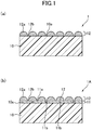
- FIGS. 1(a) and 1(b) are schematic sectional views each showing metallic lustrous member with radio wave transmissibility (hereinafter referred to as "metallic lustrous member") (1, 1A) according to a respective one of two embodiments of the present invention.
- metallic lustrous member with radio wave transmissibility
- Each of the metallic lustrous members 1, 1A comprises: a substrate 10 having radio wave transmissivity; and a metal layer 12 formed directly on a continuous surface (10a, 11a) of the substrate 10.
- a difference between the metallic lustrous member 1 and the metallic lustrous member 1A resides in that, in the metallic lustrous member 1A, an underlying layer 11 is provided on the substrate 10, which is different from the metallic lustrous member 1.
- the underlying layer 11 is provided to reduce a wettability between the metal layer 12 and the substrate 10, and, by providing the underlying layer 11, the metal layer 12 is more likely to become discontinuous.
- the underlying layer 11 is provided in the metallic lustrous member 1A, so that, differently from the continuous surface 10a in the metallic lustrous member 1, the continuous surface 11a in the metallic lustrous member 1A is not formed by the surface 10a of the substrate 10 itself, but instead formed, exactly, by the surface 11a of the underlying layer 11 provided on the substrate 10.
- This underlying layer 11 is a thin film-shaped layer, and therefore there is a possibility that a discontinuous portion 11b could be formed. However, even if such a discontinuous portion 11b is formed, the metal layer 12 never becomes discontinuous due to the discontinuous portion 11b, because the underlying layer 11 has a thickness as small as about 10 nm or less.
- the substrate 10 substantially forms the continuous surface 11a, although it includes such an underlying layer 11. Therefore, the wording "continuous surface of the substrate” in the specification encompasses not only the continuous surface 10a of the substrate itself but also the continuous surface 11a of the substrate including the underlying layer. As above, for both of the metallic lustrous members 1 and 1A, the metal layer 12 is directly formed on the continuous surface (10a, 11a) of the substrate 10, so that it is possible to significantly improve smoothness and corrosion resistance thereof, and facilitate disposing the metal layer 12 without any in-plane variation.
- the substrate 10 is required to have radio wave transmissivity, and may be, e.g., a film, a resin molded product, a glass product, or an article (body) itself to be imparted with metallic luster.
- the film is formed of a material including a homopolymer or copolymer of polyethylene terephthalate (PET), polyethylene naphthalate (PEN), polybutylene terephthalate, polyamide, polyimide, nylon, polyvinyl chloride, polycarbonate (PC), cycloolefin polymer (COP), polystyrene, polypropylene (PP), polyethylene (PE), polycycloolefin, polyurethane, polymethylmethacrylate (PMMA), or ABS.
- PET polyethylene terephthalate
- PEN polyethylene naphthalate
- PC polycarbonate
- COP cycloolefin polymer
- PP polypropylene
- PE polyethylene
- PMMA polycycloolefin
- ABS polymethylmethacrylate
- the film is transparent.
- the film is capable of withstanding high temperatures during sputtering.
- the above materials e.g., polyethylene terephthalate, polyethylene naphthalate, polycarbonate, cycloolefin polymer, polypropylene, polyurethane, polymethylmethacrylate, and ABS.
- polyethylene terephthalate, cycloolefin polymer, polycarbonate and polymethylmethacrylate are particularly preferable, because they have a good balance between heat resistance and cost.
- the substrate 10 may be a single-layer film or may be a laminate film. From a viewpoint of easy processing etc., the thickness thereof is preferably, e.g., from about 6 to 250 ⁇ m.
- the substrate 10 is a glass product
- a material for the glass product is not limited thereto.
- the substrate 10 is a resin molded product
- a material for the resin molded product is not limited thereto.
- a case where the substrate 10 is an article itself to be imparted with metallic luster is, for example, a case where the substrate 10 is used to form an emblem of an automotive vehicle, a body of a door knob of an automotive vehicle using a smart key system, a housing (outer casing) of a communication device such as a mobile phone or a personal computer, or a housing of refrigerator.
- the metal layer 12 may be provided on an outer surface of the housing, or may be provided on an inner surface of the housing.
- an article (body) to be imparted with metallic luster preferably has a similar material to that of or satisfies similar requirements to those of the above film, glass product or resin molded product.
- the continuous surface 10a of the substrate 10 may be formed of, e.g., a dielectric resin material, or a glass material.
- the continuous surface 10b of the substrate 10 may be formed of, e.g., one of a dielectric resin material, a glass material, and an indium oxide-containing material.
- the continuous surface 10a or 11a needs not necessarily be entirely formed of one of the above materials, but a specific part and the remaining part thereof may be formed of different ones of the above materials, respectively. Further, the continuous surface 10a or 11a may be only partly formed of one of the above materials.
- the dielectric resin material it is possible to use, e.g., polyester, polyolefin, acrylic-based polymer, and polycarbonate.
- the dielectric resin material includes a material obtained by forming a dielectric metal oxide material such as Al 2 O 3 , SiO 2 , Nb 2 O 3 , or TiO 2 , or a dielectric metal nitride material such as AlN or SiN, on a resin molded product such as a film.
- a dielectric metal oxide material such as Al 2 O 3 , SiO 2 , Nb 2 O 3 , or TiO 2
- a dielectric metal nitride material such as AlN or SiN
- the continuous surface 10a of the substrate 10 may be formed of a material of the resin molded product.
- the continuous surface 10a can be formed by the article itself to be imparted with metallic luster.
- the metal layer 12 can be formed directly on the substrate 10.
- the glass material it is possible to use, e.g., alkali-free glass.
- the continuous surface 10a of the substrate 10 may be formed of a material of the glass product.
- the continuous surface 10a can be formed by the article itself to be imparted with metallic luster.
- the metal layer 12 can be formed directly on the substrate 10.
- the indium oxide-containing material it is possible to use, e.g., indium oxide (In 2 O 3 ) itself, or a metal-containing material such as indium tin oxide (IOT) or indium zinc oxide (IZO).
- IOT indium tin oxide
- IZO indium zinc oxide
- ITO or IZO containing a second metal is more preferable, from a viewpoint of higher discharge stability in a sputtering process.
- the content rate by weight of tin (Sn) with respect to In 2 O 3 in ITO is, e.g., but not particularly limited to, from 2.5 wt% to 30 wt%, preferably from 3 wt% to 10 wt%.
- the content rate by weight of zinc oxide (ZnO) with respect to In 2 O 3 in IZO is, e.g., from 2 wt% to 20 wt%.
- the indium oxide-containing material is provided as the underlying layer 11 to reduce a wettability between the metal layer 12 and the substrate 10, as shown in FIG. 1(b) .
- the indium oxide-containing material substantially can form the continuous surface 11a of the substrate 10.
- the continuous surface 11a of the substrate 10 is formed of the dielectric resin material, the continuous surface 11a cannot be formed by the article itself to be imparted with metallic luster.
- the indium oxide-containing material 11 as the underlying layer may be provided directly on the surface of the substrate 10, or may be provided in an indirect manner through a protective film provided on the surface of the substrate 10.
- the thickness of the indium oxide-containing layer 11 is generally preferably 100 nm or less, more preferably 50 nm or less, still more preferably 20 nm or less.
- the thickness of the indium oxide-containing layer 11 is preferably 1 nm or more, and, from a viewpoint of reliably obtaining the discontinuous state, it is more preferably 2 nm or more, still more preferably 5 nm or more.
- the metal layer 12 is provided on the continuous surface 10a or 11a of the substrate 10 by means of AC sputtering such as MF-AC sputtering using an intermediate frequency range of, e.g., 40 KHz.
- AC sputtering such as MF-AC sputtering using an intermediate frequency range of, e.g., 40 KHz.
- each of the separated segments 12a is an aggregate of sputtered particles formed by subjecting a metal to the AC sputtering.
- easiness in forming a discontinuous structure of the metal layer 12 is relevant to surface diffusibility of the metal layer 12 on a to-be-covered member (in this embodiment, the continuous surface 11a or 11a) to be covered with the metal layer 12.
- the discontinuous structure is more likely to be formed under the condition that: the temperature of the to-be-covered member is higher; the wettability of the metal layer with respect to the to-be-covered member is smaller; and the melting point of the metal layer is lower.
- discontinuous state means a state in which the separated segments 12a are separated from each other by the interspaces 12b, and thereby electrically insulated from each other. As a result of the electrical insulation, the sheet resistance is increased, so that it becomes possible to obtain a desirable radio wave transmissibility.
- the configuration of the discontinuity is not particularly limited. For example, it may include an island-shaped configuration and a cracked configuration.
- island shape means a structure in which particles each as an aggregate of sputtered particles are independent of each other, and laid on the continuous surface 11a in slightly spaced-apart relation to each other or in partially contact relation with each other, as shown in FIG. 1(b) .
- the metal layer 12 is essentially capable of bringing out sufficient lustrousness. Further, it is desirable that the melting point thereof is relatively low. This is because the metal layer 12 is created through thin-film growth using sputtering. For this reason, a metal having a melting point of about 1000°C or less is suitable as a material for the metal layer 12.
- the metal layer 12 is preferably made of at least one metal selected from the group consisting of aluminum (Al), zinc (Zn), lead (Pb), copper (Cu) and silver (Ag), or any alloy comprising a primary component consisting of two or more of these metals. Particularly, Al and Al alloys are preferable for reason of lustrousness, stability, cost, etc., of a material. With regard to the aluminum alloy, the content rate of aluminum in the entire metal components of the alloy is preferably 50% or more, more preferably 60% or more, further preferably 75% or more.
- the thickness of the metal layer 12 is generally preferably 15 nm or more, so as to allow the metal layer 12 to bring out sufficient lustrousness, and generally preferably 80 nm or less, from a viewpoint of the sheet resistance and the radio wave transmissibility.
- the thickness of the metal layer 12 is preferably from 20 nm to 75 nm, more preferably from 25 nm to 70 nm. This thickness is suited to forming a uniform film with good productivity, and provides good external appearance of a resin molded product as a final product.
- the sheet resistance of the metal layer 12 is preferably from 100 to 100,000 ⁇ / ⁇ , so as to allow the metal layer 12 to bring out sufficient radio wave transmissibility.
- the radio wave transmissibility at a wavelength of 1 GHz is from about 10 to 0.01 [- dB]. More preferably, the sheet resistance is from 1,000 to 50,000 ⁇ / ⁇ .
- the thickness of the metal layer 12 is generally preferably 20 nm or more, so as to allow the metal layer 12 to bring out sufficient lustrousness, and generally preferably 100 nm or less, from the viewpoint of the sheet resistance and the radio wave transmissibility.
- the thickness of the metal layer 12 is preferably from 20 nm to 100 nm, more preferably from 30 nm to 70 nm.
- the preferable value is set to be larger than that in the sub-sub-section 3-2-1.
- the underlying layer 11 is a thin film-shaped layer, so that it exerts substantially no influence on the lustrousness, the sheet resistance, etc. This thickness is suited to forming a uniform film with good productivity, and provides good external appearance of a resin molded product as a final product.
- the ratio of the thickness of the metal layer to the thickness of the indium oxide-containing layer is preferably from 0.1 to 100, preferably from 0.3 to 35.
- a laminate of the metal layer 12 and the underlying layer 11 preferably has a sheet resistance of 100 to 100,000 ⁇ / ⁇ .
- the radio wave transmission attenuation amount of the laminate at a wavelength of 1 GHz is from about 10 to 0.01 [- dB]. More preferably, the radio wave transmission attenuation amount is from 1,000 to 50,000 ⁇ / ⁇ .
- the metal layer 12 is laminated directly onto the continuous surface 10a by means of the AC sputtering, without going through a step of forming the continuous surface 10a.
- the indium oxide-containing layer 11 is formed onto the substrate 10.
- the indium oxide-containing layer 11 can be formed by vacuum deposition (vacuum vapor deposition), sputtering, ion plating or the like. Among them, sputtering is preferable, from a viewpoint of being capable of strictly controlling the thickness of the indium oxide-containing layer 11 even when it has a relatively large area.
- the metal later 12 is laminated directly onto the continuous surface 11a formed by the indium oxide-containing layer 11.
- the AC sputtering is used for laminating the metal layer 12.
- the metal layer 12 is laminated such that it comes into direct contact with the indium oxide-containing layer 11 without interposing any additional layer therebetween.
- an additional layer may be interposed therebetween.
- Inventive and Comparative Examples various samples were prepared by using a film as the substrate 10. Each of the prepared samples was evaluated in terms of sheet resistance, radio wave transmission attenuation amount, and gloss value.
- the sheet resistance and the radio wave transmission attenuation amount are evaluation indexes of the radio wave transmissibility, and the gloss value is an evaluation index of the lustrousness. A larger value of each of the gloss value and the sheet resistance is more desirable, and a smaller value of the radio wave transmission attenuation amount is more desirable.
- the sheet resistance of the metal layer was measured by an eddy-current measurement method in accordance with JIS-Z2316, using a non-contact type resistance measuring device NC-80MAP manufactured by Napson Corporation.
- This sheet resistance needs to be equal to or greater than 90 ⁇ / ⁇ (ohms per square), wherein it is preferably equal to or greater than 200 ⁇ / ⁇ , more preferably equal to or greater than 250 ⁇ / ⁇ , further preferably equal to or greater than 600 ⁇ / ⁇ . If the sheet resistance is less than 90 ⁇ / ⁇ , there is a problem that a sufficient radio wave transmissibility cannot be obtained.
- a radio wave transmission attenuation amount at 1 GHz was evaluated using a KEC method measurement and evaluation jig, and a spectral analyzer CXA signal Analyzer NA9000A manufactured by Agilent technologies Inc.
- An electromagnetic wave transmissibility in a frequency band (76 to 80 GHz) of a millimeter-wave radar is correlated with an electromagnetic wave transmissibility in a microwave band (1 GHz), and thus they exhibit relatively close values.
- the radio wave transmissibility in the microwave band (1 GHz) i.e., microwave electric field transmission attenuation amount, was used as an index.
- This microwave electric field transmission attenuation amount be equal to or less than 10 [- dB], wherein it is preferably equal to or less than 5 [- dB], more preferably equal to or less than 2 [- dB]. If the microwave electric field transmission attenuation amount is greater than 10 [- dB], there is a problem that 90% or more of a radio wave is shielded.
- a 20-degree specular gloss value (degree of luster) of the metal layer was measured in accordance with JIS-Z8741, using a glossmeter PG-II M manufactured by Nippon Denshoku Industries Co.
- the gloss value has a correlation with a visible light reflectance used in the following sub-section 5-2, and thus they can be deemed to be substantially the same evaluation index.
- the gloss value which is excellent in quantitative representation of metallic luster, was used.
- the gloss value needs to be equal to or greater than 500, wherein it is preferably equal to or greater than 750, more preferably, equal to or greater than 1000. If the gloss value is less than 500, there is a problem that the lustrousness significantly deteriorates, resulting in failing to ensure excellent external appearance.
- an average of the thicknesses of the separated segments 12a is defined as the thickness of the metal layer. This average will hereinafter be referred to as "maximum thickness", for the sake of simplicity.
- the thickness of each of the separated segments 12a is defined as the largest thickness thereof as measured perpendicularly from a base (which corresponds to the continuous surface 10a or 11a in FIGS. 1(a) and 1(b) ).
- FIGS. 2(a) and 2(b) are electron microscope photographs (SEM images) each showing a surface of a metallic lustrous member with radio wave transmissibility.
- an image size of the SEM image in FIG. 2(a) is 1.16 ⁇ m ⁇ 0.85 ⁇ m
- an image size of the SEM image in FIG. 2(b) is 1.16 ⁇ m ⁇ 0.85 ⁇ m.
- a 5 cm-square region 3 as shown in FIG. 3 was appropriately extracted from the metal layer appearing on the surface of the metallic lustrous member as shown in each of FIGS. 2(a) and 2(b) , and then total five points "a” to "e” which are obtainable by dividing each of two center lines A, B of horizontal sides and the vertical sides of the square region 3 equally into four parts, are selected as measurement points.
- TEM image transmission electron microscopic photogram
- respective thicknesses of the about five separated segments 12a in each of the five measurement points i.e., about twenty-five (five segments ⁇ five points) separated segments 12a, are determined, and an average of the thicknesses of them was used as the "maximum thickness".
- a PET film manufactured by Mitsubishi Plastics, Inc. was used as a film serving as the substrate 10 (hereinafter referred to as "substrate film”). Further, an aluminum layer was used as the metal layer.
- An aluminum (Al) layer having a maximum thickness of 20 nm was formed directly on a continuous surface of the substrate film, by means of AC sputtering (MF-AC sputtering using an intermediate frequency range of 40 kHz), to obtain a metallic lustrous member (hereinafter referred to as "metal film”).
- the temperature of the substrate film during formation of the Al layer was set at 130°C, and the pressure of argon (Ar) gas in a chamber for receiving therein the substrate film was set to 2 Pa.
- the continuous surface of the substrate film exhibits high smoothness and corrosion resistance
- the aluminum layer on this continuous surface includes a plurality of separated segments 12a formed in a discontinuous state.
- the sheet resistance of the aluminum layer had a large value, and, in terms of the radio wave transmission attenuation amount, a relatively good result was shown.
- Inventive Examples 2 to 6 the maximum thickness of the aluminum layer formed on the continuous surface of the substrate film was increased in a stepwise manner, such that it becomes greater than that in Inventive Example 1. Further, in Inventive Examples 4 to 6, the pressure of the argon gas was set to a larger value than that in Inventive Example 1. The remaining conditions were the same as those in Inventive Example 1.
- FIG. 2(a) shows an SEM image of the surface of the metallic lustrous member (metal film) obtained in Inventive Example 6.
- the maximum thickness of the aluminum layer formed on the continuous surface was set to be equal to that in Inventive Example 2, and sputtering conditions, except for the temperature of the substrate film, were set in the same manner as those in Inventive Example 2. Specifically, the temperature of the substrate film was set to be lower than that in Inventive Example 2. Among Inventive Examples 7 to 11, a material for the substrate film was changed.
- polyethylene terephthalate (a PET film manufactured by Mitsubishi Chemical Co., thickness: 125 ⁇ m) was used in Inventive Example 7; polymethylmethacrylate (PMMA manufactured by Mitsubishi Chemical Corporation., thickness: 125 ⁇ m) was used in Inventive Example 8; polycarbonate (PC manufactured by Sumitomo Chemical Co., Ltd., thickness: 125 ⁇ m) was used in Inventive Example 9; alkali-free glass (manufactured by Corning Inc., thickness: 400 ⁇ m) was used in Inventive Example 10; and ITO/PET (in which the content rate by weight of tin (Sn) with respect to In 2 O 3 in ITO is 10 wt%, and the film thickness is 5 nm) was used in Inventive Example 11.
- PMMA polymethylmethacrylate
- PC PC manufactured by Sumitomo Chemical Co., Ltd., thickness: 125 ⁇ m
- alkali-free glass manufactured by Corning Inc., thickness: 400 ⁇ m
- Comparative Example 1 the maximum thickness of the aluminum layer formed on the continuous layer of the substrate film was reduced to a smaller value than those in Inventive Examples 1 to 11. On the other hand, in Comparative Example 2, the maximum thickness was increased to a larger value than those in Inventive Examples 1 to 11. Further, in Comparative Examples 1 and 2, the pressure of the argon gas was set to a lower value than those in Inventive Examples 1 to 11. The remaining conditions were the same as those in Inventive Examples 1 to 6.
- Comparative Example 1 a good result was obtained in terms of the sheet resistance and the radio wave transmissibility because of the relatively small thickness of the aluminum layer, but an insufficient result was obtained in terms of the lustrous character.
- Comparative Example 2 a sufficient result was obtained in terms of the lustrous character because of the relatively large thickness of the aluminum layer, but values of the sheet resistance and the radio wave transmissibility became worse and could not reach a level ensuring practicality.
- Vacuum deposition was used here as the film forming method. More specifically, a high-vacuum deposition apparatus EX-550 manufactured by ULVAC, Inc., was used, and a substrate was set inside a chamber thereof. After evacuating the chamber to a pressure of 10 -4 Pa, an aluminum film was formed by a resistance heating deposition method at a deposition rate of 1 nm/sec to have a thickness of 30 nm. As a result of the measurement, in terms of each of the radio wave transmissibility and the lustrousness, an insufficient result was obtained.
- Inventive and Comparative Examples various samples were prepared by using a film as the substrate 10.
- Each of the prepared samples was evaluated in terms of the sheet resistance, the radio wave transmission attenuation amount, and visible light reflectance.
- the sheet resistance and the radio wave transmission attenuation amount are evaluation indexes of the radio wave transmissibility
- the visible light reflectance is an evaluation index of the lustrousness. A larger value of each of the visible light reflectance and the sheet resistance is more desirable, and a smaller value of the radio wave transmission attenuation amount is more desirable.
- the sheet resistance was measured in a similar manner to that in the sub-sub-section 5-1-(1).
- This sheet resistance needs to be equal to or greater than 90 ⁇ / ⁇ , wherein it is preferably equal to or greater than 200 ⁇ / ⁇ , more preferably equal to or greater than 250 ⁇ / ⁇ , further preferably equal to or greater than 600 ⁇ / ⁇ . If the sheet resistance is less than 90 ⁇ / ⁇ , there is a problem that a sufficient radio wave transmissibility cannot be obtained.
- the radio wave transmission attenuation amount was measured and evaluated in a similar manner to that in the sub-sub-section 5-1-(2). More specifically, an electromagnetic wave transmissibility in a frequency band (76 to 80 GHz) of a millimeter-wave radar is correlated with an electromagnetic wave transmissibility in a microwave band (1 GHz), and thus they exhibit relatively close values. Thus, in this evaluation, the radio wave transmissibility in the microwave band (1 GHz), i.e., microwave electric field transmission attenuation amount, was used as an index.
- This microwave electric field transmission attenuation amount needs to be equal to or less than 10 [- dB], wherein it is preferably equal to or less than 5 [- dB], more preferably equal to or less than 2 [- dB]. If the microwave electric field transmission attenuation amount is greater than 10 [- dB], there is a problem that 90% or more of a radio wave is shielded.
- a reflectance at a measurement wavelength of 550 nm was measured using a spectrophotometer U4100 manufactured by Hitachi High Technologies Co., Ltd.
- the reflectance of an Al-deposited mirror was defined as a reflectance of 100%.
- the visible light reflectance need to be equal to or greater than 20%, wherein it is preferably equal to or greater than 40%, more preferably equal to or greater than 50%. If the visible light reflectance is less than 20%, there is a problem that the lustrousness significantly deteriorates, resulting in failing to ensure excellent external appearance.
- the thickness of the metal layer was measured as "maximum thickness" in a similar manner to that in the sub-sub-section 5-1-(4).
- a 50 nm-thick ITO layer was formed directly on a surface of the substrate film to extend along the surface of the substrate film.
- the temperature of the substrate film during formation of the ITO layer was set at 130°C.
- the ITO is a composition obtained by adding Sn to In 2 O 3 in an amount of 10 wt%.
- an aluminum (Al) layer having a maximum thickness of 50 nm was formed on the ITO layer to obtain a metallic lustrous member (metal film).
- the temperature of the substrate film during formation of the Al layer was set at 130°C, and the pressure of argon (Ar) gas in a chamber for receiving therein the substrate film was set to 0.22 Pa.
- FIG. 2(b) is an SEM image of the surface of the metallic lustrous member (metal film) obtained as a result of the above process
- FIG. 4 is an image of a cut surface in a partial region of FIG. 2(b) .
- An image size of the SEM image in FIG. 2(b) is 1.16 ⁇ m ⁇ 0.85 ⁇ m. It can be considered that a similar cut surface to that in FIG. 4 is obtained in each of Inventive Examples 1 to 11.
- the ITO layer is provided along the surface of the substrate film in a continuous state, it exhibits high smoothness and corrosion resistance, and, on the other hand, the aluminum layer laminated on the ITO layer includes a plurality of separated segments 12a formed in a discontinuous state, so that the sheet resistance was 260 ⁇ / ⁇ , and the radio wave transmission attenuation amount at a wavelength of 1GHz was 4.5 [- dB], i.e., in terms of the radio wave transmissibility, a good result could be obtained.
- the visible light reflectance of this metallic lustrous member was 56%, i.e., in terms of the visible light reflectance, a good result could be obtained.
- Table 1 for the sake of simplicity, with regard to a result of "evaluation" of the visible light reflectance, when a sample has a visible light reflectance of greater than 50%, the sample was evaluated as " ⁇ ", and, when a sample had a visible light reflectance of greater than 40% to 50%, the sample was evaluated as "O”. Further, when a sample had a visible light reflectance of greater than 20% to 40%, the sample was evaluated as " ⁇ ", and, when a sample had a visible light reflectance of 20% or less, the sample was evaluated as " ⁇ ".
- the thickness of the ITO layer was set to a smaller value than that in Inventive Example 12.
- the remaining conditions were the same as those in Inventive Example 12.
- the content rate of Sn in the ITO layer was changed to a larger value than that in Inventive Example 12.
- the content rate was changed to a smaller value than that in Inventive Example 12.
- the content rate of Sn in the ITO layer is set to zero.
- this layer is not an ITO layer but an indium oxide (In 2 O 3 ) layer.
- the thickness of the aluminum layer was set to 40 nm. The remaining conditions were the same as those in Inventive Example 12.
- IZO As a material for the indium oxide-containing layer, IZO obtained by adding ZnO to indium oxide was used, instead of ITO. ZnO is added to In 2 O 3 in an amount of 11 wt%. The remaining conditions were the same as those in Inventive Example 12.
- the maximum thickness of the aluminum layer laminated on the ITO layer was changed to a larger value than that in Inventive Example 12.
- the remaining conditions were the same as those in Inventive Example 12.
- the aluminum layer was formed directly on the substrate film without providing any ITO layer.
- the remaining conditions were the same as those in Inventive Example 12.
- the metal layer 12 formed in the metallic lustrous member 1A has a small thickness of about 20 to 100 nm, and can be used by itself as a metal thin film.
- the metal layer 12 may be formed by sputtering on the indium oxide-containing layer 11 laminated on a substrate such as the substrate 10, to obtain a film. Further, separately from this, an adhesive is applied onto a substrate to produce an adhesive layer-attached substrate. Then, the film is laminated to the adhesive layer-attached substrate, such that the metal layer 12 comes in contact with the adhesive layer.
- the metal layer (metal thin film) 12 which has been located on the outermost surface side of the film can be transferred to the outermost surface side of the adhesive layer-attached substrate, by separating the film and the substrate from each other, after fully having contacted them.
- the metal film or the metallic lustrous member according to the present invention can be suitably used, e.g., to decorate a cover member of a millimeter-wave radar mounted to a front component such as a front grille or an emblem at a front end of an automotive vehicle.
- the present invention may also be applied to various other articles requiring both an aesthetic quality and radio wave transmissibility, such as a mobile phone, a smart phone, a tablet PC, a notebook PC, and a refrigerator.
Landscapes
- Chemical & Material Sciences (AREA)
- Engineering & Computer Science (AREA)
- Chemical Kinetics & Catalysis (AREA)
- Materials Engineering (AREA)
- Organic Chemistry (AREA)
- Mechanical Engineering (AREA)
- Metallurgy (AREA)
- General Chemical & Material Sciences (AREA)
- Life Sciences & Earth Sciences (AREA)
- Geochemistry & Mineralogy (AREA)
- Ceramic Engineering (AREA)
- Physical Vapour Deposition (AREA)
- Laminated Bodies (AREA)
- Surface Treatment Of Glass (AREA)
- Details Of Aerials (AREA)
- Radar Systems Or Details Thereof (AREA)
Abstract
Description
- Metallic lustrous member with radio wave transmissibility, article using same, and production method therefor
- The present invention relates to a metallic lustrous member with radio wave transmissibility, an article using the member, and a production method for the member or the article.
- A metallic lustrous member having both lustrousness and radio wave transmissibility (permeability) is needed, for example, to decorate a cover member of a millimeter-wave radar mounted to a front component such as a front grille or an emblem at a front end of an automotive vehicle.
- The millimeter-wave radar is configured to transmit an electromagnetic wave having a millimeter waveband (frequency: about 77 GHz, wavelength: about 4 mm) forwardly with respect to the vehicle, and receive and analyze a reflected wave from a target so as to measure a distance or a direction with respect to the target, or the size of the target. A result of the measurement can be utilized for inter-vehicle distance measurement, automatic vehicle speed adjustment, automatic brake adjustment, etc. The front component of the vehicle to which the millimeter-wave radar is mounted is a portion constituting, so to say, the face of the vehicle, and giving a profound impression on a user. Thus, it is preferable to create a high-class appearance or the like by a metallic lustrous front decoration. However, if the front component of the vehicle is made of a metal material, it will substantially preclude or hinder the millimeter-wave radar from emitting and receiving an electromagnetic wave. Therefore, in order to prevent hindering of the function of the millimeter-wave radar without spoiling an aesthetic appearance of the vehicle, there is a need for a metallic lustrous member having both lustrousness and radio wave transmissibility.
- In addition to application to millimeter-wave radars, this type of metallic lustrous member is expected to be applied to various other devices requiring signal transmitting-receiving, e.g., a door handle module of an automotive vehicle using a smart key system, in-vehicle communication devices, and electronic devices such as a mobile phone and a personal computer. Further, in recent years, along with development in IoT technologies, the metallic lustrous member is also expected to be applied to a wide range of fields, e.g., home or daily-life appliances such as a refrigerator, in which signal transmitting-receiving has heretofore not been performed.
- With regard to the metallic lustrous member, in
JP 2007-144988A Patent Document 1, the inorganic underlying film is composed of (a) a thin film of a metal compound such as: a titanium compound including titanium oxide (TiO, TiO2, Ti3O5, etc.); a silicon compound including silicon oxide (SiO, SiO2, etc.) or silicon nitride (Si3N4, etc.); an aluminum compound including aluminum oxide (Al2O3); an iron compound including iron oxide (Fe2O3); a selenium compound including selenium oxide (CeO); a zircon compound including zircon oxide (ZrO); or a zinc compound including zinc sulfide (ZnS), or (b) a coating film made of an inorganic coating material, e.g., a coating film made of an inorganic coating material comprising a primary component consisting of silicon, amorphousTiO2 or the like (additionally, any of the metal compounds exemplified above). However, this resin product is based on the assumption of using only chromium (Cr) or indium (In) as a material for the metal film. In other words, a metal superior to chromium and indium in terms of cost and lustrousness, such as aluminum (Al), cannot be used as a material for the metal film. - Further, in
JP 2009-298006A -
- Patent Document 1:
JP 2007-144988A - Patent Document 2:
JP2009-298006A - The present invention has been made to solve the above conventional problems, and an object thereof is to provide a metallic lustrous member with radio wave transmissibility, which is capable of being easily produced, wherein not only chromium (Cr) or indium (In) but also any of some other metals such as aluminum (Al) is formed as a metal layer on a continuous surface of any of various materials, and an article using the member. It is another object of the present invention to provide a production method for a metallic lustrous member with radio wave transmissibility, or an article using the member, which is capable of easily forming, as a metal layer, not only chromium (Cr) or indium (In) but also any of some other metals such as aluminum (Al), on a continuous surface of any of various materials.
- As a result of diligent studies for solving the above problems, the present inventors found that, by using AC (alternating current) sputtering, it becomes possible to cause a metal which normally has difficulty in being formed into a discontinuous structure, such as aluminum (Al), to develop a discontinuous structure on a continuous surface of any of various materials, and have reached accomplishment of the present invention.
- In order to solve the above problems, according to a first aspect of the present invention, there is provided a metallic lustrous member with radio wave transmissibility, which comprises: a substrate having radio wave transmissibility; and an aluminum layer formed directly on a continuous surface of the substrate, wherein the aluminum layer has a discontinuous region including a plurality of separated segments which are mutually discontinuous.
- The metallic lustrous member according to the first aspect of the present invention is capable of being easily produced, while ensuring a structure in which not only chromium (Cr) or indium (In) but also any of some other metals such as aluminum (Al) is formed as a metal layer on a continuous surface of any of various materials.
- Preferably, in the metallic lustrous member according to the first aspect of the present invention, the aluminum layer has a sheet resistance of 90 Ω/□ or more.
- In order to solve the above problems, according to a second aspect of the present invention, there is provided a metallic lustrous member with radio wave transmissibility, which comprises: a substrate having radio wave transmissibility; and an aluminum layer formed directly on a continuous surface of the substrate, wherein the member has a sheet resistance of 90 Ω/□ or more.
- The metallic lustrous member according to the second aspect of the present invention is capable of being easily produced, while ensuring a structure in which not only chromium (Cr) or indium (In) but also any of some other metals such as aluminum (Al) is formed as a metal layer on a continuous surface of any of various materials.
- In the metallic lustrous member according to the first or second aspect of the present invention, the continuous surface may be formed of a dielectric resin material or a glass material. Here, the dielectric resin material may be comprised of any one of polyester, polyolefin, acrylic-based polymer, and polycarbonate.
- In the metallic lustrous member according to the first or second aspect of the present invention, the continuous surface may be formed using an indium oxide-containing material.
- In the metallic lustrous member according to the first or second aspect of the present invention, the substrate may be one selected from the group consisting of a film, a resin molded product, a glass product, and an article itself to be imparted with metallic luster.
- Preferably, in the metallic lustrous member according to the first or second aspect of the present invention, the aluminum layer has a maximum thickness of 15 to 80 nm.
- Preferably, in the metallic lustrous member according to the first or second aspect of the present invention, the aluminum layer has a radio wave transmission attenuation amount of 10 dB or less.
- In the metallic lustrous member according to the first or second aspect of the present invention, the aluminum layer may be one of aluminum (Al) and an aluminum (Al) alloy. Here, a content ratio of aluminum to an entire metal component in the aluminum (Al) alloy is preferably 50% or more.
- In the metallic lustrous member according to the first or second aspect of the present invention, the aluminum layer may be provided on an inner surface of a transparent housing formed using the continuous surface of the substrate.
- According to a third aspect of the present invention, there is provided a production method for a metallic lustrous member with radio wave transmissibility, or an article using the member. The production method comprises the step of forming an aluminum layer directly on a substrate having radio wave transmissibility by means of AC sputtering, wherein the aluminum layer has a discontinuous region including a plurality of separated segments which are mutually discontinuous.
- According to a fourth aspect of the present invention, there is provided a production method for a metallic lustrous member with radio wave transmissibility, or an article using the member. The production method comprises the step of forming an aluminum layer directly on a substrate having radio wave transmissibility by means of AC sputtering, such that the aluminum layer has a sheet resistance of 90 Ω/□ or more
- The production method according to the third or fourth aspect of the present invention makes it possible to easily form, as a metal layer, not only chromium (Cr) or indium (In) but also any of some other metals such as aluminum (Al), on a continuous surface of any of various materials.
- In the production method according to the third or fourth aspect of the present invention, the aluminum layer may be formed directly on a continuous surface of the substrate. Here, the continuous surface may be formed of a dielectric resin material or a glass material, or may be formed using an indium oxide-containing material.
- Preferably, in the production method according to the third or fourth aspect of the present invention, the AC sputtering is performed under a pressure of 1.5 Pa or more.
- Preferably, in the production method according to the third or fourth aspect of the present invention, during the AC sputtering, the substrate has a temperature of 20°C or more.
- The present invention provides: a metallic lustrous member with radio wave transmissibility, which is capable of being easily produced, wherein a surface on which a metal layer is to be formed may be a continuous surface, and not only chromium (Cr) or indium (In) but also any of some other metals such as aluminum (Al) is usable as the metal layer; an article using the member; and a production method therefor.
-
-
FIGS. 1(a) and 1(b) are schematic sectional views each showing a metallic lustrous member with radio wave transmissibility according to a respective one of two embodiments of the present invention. -
FIGS. 2(a) and 2(b) are electron microscope photographs each showing a surface of a metallic lustrous member with radio wave transmissibility according to one embodiment of the present invention. -
FIG. 3 is a diagram for explaining a method of measuring the thickness of a metal layer in each of Inventive and Comparative Examples. -
FIG. 4 is an image of a cut surface in a partial region ofFIG. 2(b) . - With reference to the accompanying drawings, a preferred embodiment of the present invention will now be described. Although only the preferred embodiment of the present invention will be shown in the following for the sake of convenience of explanation, it should be understood that the present invention is not limited thereto.
-
FIGS. 1(a) and 1(b) are schematic sectional views each showing metallic lustrous member with radio wave transmissibility (hereinafter referred to as "metallic lustrous member") (1, 1A) according to a respective one of two embodiments of the present invention. In these figures and other figures, the same or corresponding elements or members are assigned with the same reference sign. - Each of the metallic
lustrous members substrate 10 having radio wave transmissivity; and ametal layer 12 formed directly on a continuous surface (10a, 11a) of thesubstrate 10. A difference between the metalliclustrous member 1 and the metalliclustrous member 1A resides in that, in the metalliclustrous member 1A, an underlying layer 11 is provided on thesubstrate 10, which is different from the metalliclustrous member 1. The underlying layer 11 is provided to reduce a wettability between themetal layer 12 and thesubstrate 10, and, by providing the underlying layer 11, themetal layer 12 is more likely to become discontinuous. The underlying layer 11 is provided in the metalliclustrous member 1A, so that, differently from thecontinuous surface 10a in the metalliclustrous member 1, thecontinuous surface 11a in the metalliclustrous member 1A is not formed by thesurface 10a of thesubstrate 10 itself, but instead formed, exactly, by thesurface 11a of the underlying layer 11 provided on thesubstrate 10. This underlying layer 11 is a thin film-shaped layer, and therefore there is a possibility that adiscontinuous portion 11b could be formed. However, even if such adiscontinuous portion 11b is formed, themetal layer 12 never becomes discontinuous due to thediscontinuous portion 11b, because the underlying layer 11 has a thickness as small as about 10 nm or less. In other words, even supposing that there is thediscontinuous portion 11b in the underlying layer 11, it can be understood that, with regard to a relationship with themetal layer 12, thesubstrate 10 substantially forms thecontinuous surface 11a, although it includes such an underlying layer 11. Therefore, the wording "continuous surface of the substrate" in the specification encompasses not only thecontinuous surface 10a of the substrate itself but also thecontinuous surface 11a of the substrate including the underlying layer. As above, for both of the metalliclustrous members metal layer 12 is directly formed on the continuous surface (10a, 11a) of thesubstrate 10, so that it is possible to significantly improve smoothness and corrosion resistance thereof, and facilitate disposing themetal layer 12 without any in-plane variation. - The
substrate 10 is required to have radio wave transmissivity, and may be, e.g., a film, a resin molded product, a glass product, or an article (body) itself to be imparted with metallic luster. - In a case where the
substrate 10 is a film, the film is formed of a material including a homopolymer or copolymer of polyethylene terephthalate (PET), polyethylene naphthalate (PEN), polybutylene terephthalate, polyamide, polyimide, nylon, polyvinyl chloride, polycarbonate (PC), cycloolefin polymer (COP), polystyrene, polypropylene (PP), polyethylene (PE), polycycloolefin, polyurethane, polymethylmethacrylate (PMMA), or ABS. These materials have no influence on lustrousness and radio wave transmissibility. Preferably, the film is transparent. Further, from a viewpoint of subsequently forming themetal layer 12 thereon, it is desirable that the film is capable of withstanding high temperatures during sputtering. Thus, among the above materials, e.g., polyethylene terephthalate, polyethylene naphthalate, polycarbonate, cycloolefin polymer, polypropylene, polyurethane, polymethylmethacrylate, and ABS, are preferable. Among them, polyethylene terephthalate, cycloolefin polymer, polycarbonate and polymethylmethacrylate are particularly preferable, because they have a good balance between heat resistance and cost. Thesubstrate 10 may be a single-layer film or may be a laminate film. From a viewpoint of easy processing etc., the thickness thereof is preferably, e.g., from about 6 to 250 µm. - In a case where the
substrate 10 is a glass product, it is possible to use, e.g., a soda-lime glass, an alkali-free glass, and a chemically strengthened glass. However, a material for the glass product is not limited thereto. - In a case where the
substrate 10 is a resin molded product, it is possible to use, e.g., ABS, PC, PMMA, PP, PE, polyphthalamide (PPA), polyoxymethylene (POM), and polybutylene terephthalate (PBT). However, a material for the resin molded product is not limited thereto. - A case where the
substrate 10 is an article itself to be imparted with metallic luster, is, for example, a case where thesubstrate 10 is used to form an emblem of an automotive vehicle, a body of a door knob of an automotive vehicle using a smart key system, a housing (outer casing) of a communication device such as a mobile phone or a personal computer, or a housing of refrigerator. In a case where the housing of a communication device or the like is transparent, themetal layer 12 may be provided on an outer surface of the housing, or may be provided on an inner surface of the housing. However, an article (body) to be imparted with metallic luster preferably has a similar material to that of or satisfies similar requirements to those of the above film, glass product or resin molded product. - The
continuous surface 10a of thesubstrate 10 may be formed of, e.g., a dielectric resin material, or a glass material. On the other hand, the continuous surface 10b of thesubstrate 10 may be formed of, e.g., one of a dielectric resin material, a glass material, and an indium oxide-containing material. Thecontinuous surface continuous surface - As the dielectric resin material, it is possible to use, e.g., polyester, polyolefin, acrylic-based polymer, and polycarbonate. The dielectric resin material includes a material obtained by forming a dielectric metal oxide material such as Al2O3, SiO2, Nb2O3, or TiO2, or a dielectric metal nitride material such as AlN or SiN, on a resin molded product such as a film. For example, as shown in
FIG. 1(a) , when thesubstrate 10 is the resin molded product, thecontinuous surface 10a of thesubstrate 10 may be formed of a material of the resin molded product. In this case, thecontinuous surface 10a can be formed by the article itself to be imparted with metallic luster. In other words, themetal layer 12 can be formed directly on thesubstrate 10. - As the glass material, it is possible to use, e.g., alkali-free glass. For example, as shown in
FIG. 1(a) , when thesubstrate 10 is the glass product, thecontinuous surface 10a of thesubstrate 10 may be formed of a material of the glass product. In this case, thecontinuous surface 10a can be formed by the article itself to be imparted with metallic luster. In other words, themetal layer 12 can be formed directly on thesubstrate 10. - As the indium oxide-containing material, it is possible to use, e.g., indium oxide (In2O3) itself, or a metal-containing material such as indium tin oxide (IOT) or indium zinc oxide (IZO). However, ITO or IZO containing a second metal is more preferable, from a viewpoint of higher discharge stability in a sputtering process. The content rate by weight of tin (Sn) with respect to In2O3 in ITO is, e.g., but not particularly limited to, from 2.5 wt% to 30 wt%, preferably from 3 wt% to 10 wt%. Further, the content rate by weight of zinc oxide (ZnO) with respect to In2O3 in IZO is, e.g., from 2 wt% to 20 wt%. The indium oxide-containing material is provided as the underlying layer 11 to reduce a wettability between the
metal layer 12 and thesubstrate 10, as shown inFIG. 1(b) . Thus, the indium oxide-containing material substantially can form thecontinuous surface 11a of thesubstrate 10. However, in the case where thecontinuous surface 11a of thesubstrate 10 is formed of the dielectric resin material, thecontinuous surface 11a cannot be formed by the article itself to be imparted with metallic luster. The indium oxide-containing material 11 as the underlying layer may be provided directly on the surface of thesubstrate 10, or may be provided in an indirect manner through a protective film provided on the surface of thesubstrate 10. From a viewpoint of sheet resistance, radio wave transmissibility and productivity, the thickness of the indium oxide-containing layer 11 is generally preferably 100 nm or less, more preferably 50 nm or less, still more preferably 20 nm or less. On the other hand, from a viewpoint of laminating themetal layer 12 in a discontinuous state, the thickness of the indium oxide-containing layer 11 is preferably 1 nm or more, and, from a viewpoint of reliably obtaining the discontinuous state, it is more preferably 2 nm or more, still more preferably 5 nm or more. - The
metal layer 12 is provided on thecontinuous surface substrate 10 by means of AC sputtering such as MF-AC sputtering using an intermediate frequency range of, e.g., 40 KHz. By using the AC sputtering to provide themetal layer 12, it becomes possible to allow themetal layer 12 to be formed such that it has, on at least a part of thecontinuous surface segments 12a which are mutually discontinuous, and, more specifically, separated from each other byinterspaces 12b. Since the separatedsegments 12a are separated from each other by theinterspaces 12b, a sheet resistance in the separatedsegments 12a is increased, and a radio wave transmission attenuation amount in the separatedsegments 12a is reduced, so that an interaction of the separatedsegments 12a with electromagnetic waves is weakened to allow electromagnetic waves to be transmitted through themetal layer 12. Each of the separatedsegments 12a is an aggregate of sputtered particles formed by subjecting a metal to the AC sputtering. Although details of a mechanism causing themetal layer 12 to become a discontinuous state on thecontinuous surface metal layer 12, easiness in forming a discontinuous structure of themetal layer 12 is relevant to surface diffusibility of themetal layer 12 on a to-be-covered member (in this embodiment, thecontinuous surface metal layer 12. Specifically, the discontinuous structure is more likely to be formed under the condition that: the temperature of the to-be-covered member is higher; the wettability of the metal layer with respect to the to-be-covered member is smaller; and the melting point of the metal layer is lower. Therefore, with regard to some metals other than aluminum (Al) used particularly in the following Examples, such as zinc (Zn), lead (Pb), copper (Cu) and silver (Ag) each having a relatively low melting point, the discontinuous structure is considered to be able to be formed in a similar manner. It should be noted here that the term "discontinuous state" as used in this specification means a state in which the separatedsegments 12a are separated from each other by theinterspaces 12b, and thereby electrically insulated from each other. As a result of the electrical insulation, the sheet resistance is increased, so that it becomes possible to obtain a desirable radio wave transmissibility. The configuration of the discontinuity is not particularly limited. For example, it may include an island-shaped configuration and a cracked configuration. Here, the term "island shape" means a structure in which particles each as an aggregate of sputtered particles are independent of each other, and laid on thecontinuous surface 11a in slightly spaced-apart relation to each other or in partially contact relation with each other, as shown inFIG. 1(b) . - The
metal layer 12 is essentially capable of bringing out sufficient lustrousness. Further, it is desirable that the melting point thereof is relatively low. This is because themetal layer 12 is created through thin-film growth using sputtering. For this reason, a metal having a melting point of about 1000°C or less is suitable as a material for themetal layer 12. For example, themetal layer 12 is preferably made of at least one metal selected from the group consisting of aluminum (Al), zinc (Zn), lead (Pb), copper (Cu) and silver (Ag), or any alloy comprising a primary component consisting of two or more of these metals. Particularly, Al and Al alloys are preferable for reason of lustrousness, stability, cost, etc., of a material. With regard to the aluminum alloy, the content rate of aluminum in the entire metal components of the alloy is preferably 50% or more, more preferably 60% or more, further preferably 75% or more. - In the case where the continuous surface is formed by the
surface 10a of thesubstrate 10 itself, and themetal layer 12 is formed directly on thiscontinuous surface 10a, as shown inFIG. 1(a) , the thickness of themetal layer 12 is generally preferably 15 nm or more, so as to allow themetal layer 12 to bring out sufficient lustrousness, and generally preferably 80 nm or less, from a viewpoint of the sheet resistance and the radio wave transmissibility. For example, the thickness of themetal layer 12 is preferably from 20 nm to 75 nm, more preferably from 25 nm to 70 nm. This thickness is suited to forming a uniform film with good productivity, and provides good external appearance of a resin molded product as a final product. - Further, the sheet resistance of the
metal layer 12 is preferably from 100 to 100,000 Ω/□, so as to allow themetal layer 12 to bring out sufficient radio wave transmissibility. In this case, the radio wave transmissibility at a wavelength of 1 GHz is from about 10 to 0.01 [- dB]. More preferably, the sheet resistance is from 1,000 to 50,000 Ω/□. - In the case where the
continuous surface 11a is formed by the surface of the underlying layer 11, and themetal layer 12 is formed directly on thiscontinuous surface 11a of thesubstrate 10, as shown inFIG. 1(b) , the thickness of themetal layer 12 is generally preferably 20 nm or more, so as to allow themetal layer 12 to bring out sufficient lustrousness, and generally preferably 100 nm or less, from the viewpoint of the sheet resistance and the radio wave transmissibility. For example, the thickness of themetal layer 12 is preferably from 20 nm to 100 nm, more preferably from 30 nm to 70 nm. As above, the preferable value is set to be larger than that in the sub-sub-section 3-2-1. This is because, as a result of providing the underlying layer 11, the wettability between themetal layer 12 and thesubstrate 10 is reduced, and thereby themetal layer 12 becomes more likely to be formed as a discontinuous layer, so that it is possible to increase the thickness of themetal layer 12. Here, the underlying layer 11 is a thin film-shaped layer, so that it exerts substantially no influence on the lustrousness, the sheet resistance, etc. This thickness is suited to forming a uniform film with good productivity, and provides good external appearance of a resin molded product as a final product. - Further, for the similar reasons, in a case where the underlying layer 11 is, e.g., an indium oxide-containing layer, the ratio of the thickness of the metal layer to the thickness of the indium oxide-containing layer (the thickness of the metal layer / the thickness of the indium oxide-containing layer) is preferably from 0.1 to 100, preferably from 0.3 to 35.
- Further, a laminate of the
metal layer 12 and the underlying layer 11 preferably has a sheet resistance of 100 to 100,000 Ω/□. In this case, the radio wave transmission attenuation amount of the laminate at a wavelength of 1 GHz is from about 10 to 0.01 [- dB]. More preferably, the radio wave transmission attenuation amount is from 1,000 to 50,000 Ω/□. - One example of a production method for each of the metallic
lustrous members - In the case where the
continuous surface 10a is formed by the surface of thesubstrate 10 itself, and themetal layer 12 is formed directly on thiscontinuous surface 10a, as shown inFIG. 1(a) , themetal layer 12 is laminated directly onto thecontinuous surface 10a by means of the AC sputtering, without going through a step of forming thecontinuous surface 10a. - In the case where the
continuous surface 11a is formed by the surface of the underlying layer 11, and themetal layer 12 is formed directly on thiscontinuous surface 11a, as shown inFIG. 1(b) , at least two steps are needed. - The indium oxide-containing layer 11 is formed onto the
substrate 10. The indium oxide-containing layer 11 can be formed by vacuum deposition (vacuum vapor deposition), sputtering, ion plating or the like. Among them, sputtering is preferable, from a viewpoint of being capable of strictly controlling the thickness of the indium oxide-containing layer 11 even when it has a relatively large area. - Subsequently, the metal later 12 is laminated directly onto the
continuous surface 11a formed by the indium oxide-containing layer 11. The AC sputtering is used for laminating themetal layer 12. Preferably, themetal layer 12 is laminated such that it comes into direct contact with the indium oxide-containing layer 11 without interposing any additional layer therebetween. However, as long as the above mechanism based on surface diffusibility of themetal layer 12 on the indium oxide-containing layer 11 effectively functions, an additional layer may be interposed therebetween. - In Inventive and Comparative Examples, various samples were prepared by using a film as the
substrate 10. Each of the prepared samples was evaluated in terms of sheet resistance, radio wave transmission attenuation amount, and gloss value. The sheet resistance and the radio wave transmission attenuation amount are evaluation indexes of the radio wave transmissibility, and the gloss value is an evaluation index of the lustrousness. A larger value of each of the gloss value and the sheet resistance is more desirable, and a smaller value of the radio wave transmission attenuation amount is more desirable. - Details of evaluation methods are as follows.
- The sheet resistance of the metal layer was measured by an eddy-current measurement method in accordance with JIS-Z2316, using a non-contact type resistance measuring device NC-80MAP manufactured by Napson Corporation.
- This sheet resistance needs to be equal to or greater than 90 Ω/□ (ohms per square), wherein it is preferably equal to or greater than 200 Ω/□, more preferably equal to or greater than 250 Ω/□, further preferably equal to or greater than 600 Ω/□. If the sheet resistance is less than 90 Ω/□, there is a problem that a sufficient radio wave transmissibility cannot be obtained.
- A radio wave transmission attenuation amount at 1 GHz was evaluated using a KEC method measurement and evaluation jig, and a spectral analyzer CXA signal Analyzer NA9000A manufactured by Agilent technologies Inc. An electromagnetic wave transmissibility in a frequency band (76 to 80 GHz) of a millimeter-wave radar is correlated with an electromagnetic wave transmissibility in a microwave band (1 GHz), and thus they exhibit relatively close values. Thus, in this evaluation, the radio wave transmissibility in the microwave band (1 GHz), i.e., microwave electric field transmission attenuation amount, was used as an index.
- This microwave electric field transmission attenuation amount be equal to or less than 10 [- dB], wherein it is preferably equal to or less than 5 [- dB], more preferably equal to or less than 2 [- dB]. If the microwave electric field transmission attenuation amount is greater than 10 [- dB], there is a problem that 90% or more of a radio wave is shielded.
- A 20-degree specular gloss value (degree of luster) of the metal layer was measured in accordance with JIS-Z8741, using a glossmeter PG-II M manufactured by Nippon Denshoku Industries Co. The gloss value has a correlation with a visible light reflectance used in the following sub-section 5-2, and thus they can be deemed to be substantially the same evaluation index. However, the gloss value, which is excellent in quantitative representation of metallic luster, was used.
- In order to have sufficient lustrousness, the gloss value needs to be equal to or greater than 500, wherein it is preferably equal to or greater than 750, more preferably, equal to or greater than 1000. If the gloss value is less than 500, there is a problem that the lustrousness significantly deteriorates, resulting in failing to ensure excellent external appearance.
- In Inventive and Comparative Examples, considering variation in thickness of the metal layer, more specifically, variation in thickness between the separated
segments 12a illustrated inFIG. 1 , an average of the thicknesses of the separatedsegments 12a is defined as the thickness of the metal layer. This average will hereinafter be referred to as "maximum thickness", for the sake of simplicity. Here, the thickness of each of the separatedsegments 12a is defined as the largest thickness thereof as measured perpendicularly from a base (which corresponds to thecontinuous surface FIGS. 1(a) and 1(b) ). -
FIGS. 2(a) and 2(b) are electron microscope photographs (SEM images) each showing a surface of a metallic lustrous member with radio wave transmissibility. Here, an image size of the SEM image inFIG. 2(a) is 1.16 µm × 0.85 µm, and an image size of the SEM image inFIG. 2(b) is 1.16 µm × 0.85 µm. When determining the maximum thickness, a 5 cm-square region 3 as shown inFIG. 3 was appropriately extracted from the metal layer appearing on the surface of the metallic lustrous member as shown in each ofFIGS. 2(a) and 2(b) , and then total five points "a" to "e" which are obtainable by dividing each of two center lines A, B of horizontal sides and the vertical sides of thesquare region 3 equally into four parts, are selected as measurement points. - Subsequently, in a cross-sectional image (transmission electron microscopic photogram (TEM image)) as shown in
FIG. 4 , at each of the selected measurement points, a view-angle region including about five separatedsegments 12a was extracted. - Subsequently, respective thicknesses of the about five separated
segments 12a in each of the five measurement points, i.e., about twenty-five (five segments × five points) separatedsegments 12a, are determined, and an average of the thicknesses of them was used as the "maximum thickness". - Results of the evaluations are shown in the following Table 1.
TABLE 1 Metal Layer Sputtering Conditions Subst rate Film Radio Wave Transmissibility Lustrousness Compre hensive Evaluati on Sheet Resistance Radio Wave Transmission Attenuation Amount @ 1GHz Evalua tion Gloss Value GS20° Evalua tion Mater ial Maximum Thickness (nm) Film Forming Method Substrate Temperature (° C) Ar Gas Pressure (Pa) Mater ial [Ω /□] [- dB] [-] Inventive Example 1 Al 20 MF-AC sputtering 130 2 PET > 3K 0.02 ⊚ 601 Δ ○ Inventive Example 2 Al 30 MF-AC sputtering 130 2 PET > 3K 0.02 ⊚ 750 Δ ○ Inventive Example 3 Al 40 MF-AC sputtering 130 2 PET > 3K 0.03 ⊚ 825 ○ ○ Inventive Example 4 Al 50 MF-AC sputtering 130 3 PET > 3K 0.05 ⊚ 915 ○ ○ Inventive Example 5 Al 60 MF-AC sputtering 130 3 PET 320 3.7 ○ 1020 ⊚ ○ Inventive Example 6 Al 70 MF-AC sputtering 130 3 PET 180 5.4 Δ 1130 ⊚ ○ Inventive Example 7 Al 30 MF-AC sputtering 25 2 PET > 3K 0.3 ⊚ 920 ○ ○ Inventive Example 8 Al 30 MF-AC sputtering 25 2 PMM A > 3K 0.2 ⊚ 892 ○ ○ Inventive Example 9 Al 30 MF-AC sputtering 25 2 PC > 3K 0.3 ⊚ 930 ○ ○ Inventive Example 10 Al 30 MF-AC sputtering 25 2 Glass > 3K 0.3 ⊚ 1104 ⊚ ○ Inventive Example 11 Al 30 MF-AC sputtering 25 2 ITO/ PET > 3K 0.03 ⊚ 763 ○ ○ Comparat ive Example 1 Al 10 MF-AC sputtering 130 1 PET > 3K 0.02 ⊚ 307 × × Comparat ive Example 2 Al 100 MF-AC sputtering 130 1 PET 0.6 45.1 × 1850 ⊚ × Comparat ive Example 3 Al 30 DC sputtering 130 1 PET 1.3 40.2 × 1632 ⊚ × Comparat ive Example 4 Al 30 Vacuum deposition 25 0.0001 PET 2.4 35.6 × 1570 ⊚ × - A PET film manufactured by Mitsubishi Plastics, Inc. (thickness: 125 µm) was used as a film serving as the substrate 10 (hereinafter referred to as "substrate film"). Further, an aluminum layer was used as the metal layer. An aluminum (Al) layer having a maximum thickness of 20 nm was formed directly on a continuous surface of the substrate film, by means of AC sputtering (MF-AC sputtering using an intermediate frequency range of 40 kHz), to obtain a metallic lustrous member (hereinafter referred to as "metal film"). The temperature of the substrate film during formation of the Al layer was set at 130°C, and the pressure of argon (Ar) gas in a chamber for receiving therein the substrate film was set to 2 Pa.
- In the metal film of Inventive Example 1, the continuous surface of the substrate film exhibits high smoothness and corrosion resistance, and, on the other hand, the aluminum layer on this continuous surface includes a plurality of separated
segments 12a formed in a discontinuous state. Thus, the sheet resistance of the aluminum layer had a large value, and, in terms of the radio wave transmission attenuation amount, a relatively good result was shown. In Table 1, for the sake of simplicity, with regard to a result of "evaluation" of the radio wave transmission attenuation amount, when a sample had a radio wave transmission attenuation amount of less than 2 [- dB], the sample was evaluated as "⊚", and, when a sample had a radio wave transmission attenuation amount of 2 [- dB] to less than 5 [- dB], the sample was evaluated as "O". Further, when a sample had a radio wave transmission attenuation amount of 5 [- dB] to less than 10 [- dB], the sample was evaluated as "Δ", and, when a sample had a radio wave transmission attenuation amount of 10 [- dB] or more, the sample was evaluated as " ×". - Further, in the metal film of Inventive Example 1, in terms of the lustrousness, a result ensuring sufficient practicality was also obtained. In Table 1, for the sake of simplicity, with regard to a result of "evaluation" of the gloss value, when a sample has a gloss value of 1000 or more, the sample was evaluated as "⊚", and, when a sample had a lustrousness of 750 to less than 1000, the sample was evaluated as "O". Further, when a sample had a lustrousness of 500 to less than 750, the sample was evaluated as " Δ", and, when a sample had a lustrousness of less than 500, the sample was evaluated as "×". Further, with regard to "comprehensive evaluation" of the radio wave transmissibility and the lustrousness, when a sample was evaluated as "×" in any of the evaluations, the sample was comprehensively evaluated as "×", and, in any other case, a sample was comprehensively evaluated as "○". As a result, in Inventive Example 1, the comprehensive evaluation was "○", i.e., a good metallic lustrous member or metal film having both the radio wave transmissibility and the lustrousness could be obtained.
- In Inventive Examples 2 to 6, the maximum thickness of the aluminum layer formed on the continuous surface of the substrate film was increased in a stepwise manner, such that it becomes greater than that in Inventive Example 1. Further, in Inventive Examples 4 to 6, the pressure of the argon gas was set to a larger value than that in Inventive Example 1. The remaining conditions were the same as those in Inventive Example 1.
- With regard to the sheet resistance, in Inventive Examples 2 to 4, a large value of greater than 3 kQ was obtained, as with Inventive Example 1. On the other hand, in Inventive Examples 5 and 6, a practically sufficiently large value was obtained although it is not as high as those in Inventive Examples 2 to 4. The reason why the sheet resistance in Inventive Examples 5 and 6 becomes lower than that in Inventive Example 1 is considered that the amount of deposition of aluminum is excessively increased, thereby causing a decrease in the discontinuous region. With regard to the radio wave transmissibility, in all of Inventive Examples 2 to 6, results equivalent to or better than that in Inventive Example 1 were obtained. Further, with regard to the gloss value, in all of Inventive Examples 2 to 6, results better than that in Inventive Example 1 were of course obtained.
-
FIG. 2(a) shows an SEM image of the surface of the metallic lustrous member (metal film) obtained in Inventive Example 6. - In all of Inventive Examples 7 to 11, the maximum thickness of the aluminum layer formed on the continuous surface was set to be equal to that in Inventive Example 2, and sputtering conditions, except for the temperature of the substrate film, were set in the same manner as those in Inventive Example 2. Specifically, the temperature of the substrate film was set to be lower than that in Inventive Example 2. Among Inventive Examples 7 to 11, a material for the substrate film was changed. Specifically, polyethylene terephthalate (a PET film manufactured by Mitsubishi Chemical Co., thickness: 125 µm) was used in Inventive Example 7; polymethylmethacrylate (PMMA manufactured by Mitsubishi Chemical Corporation., thickness: 125 µm) was used in Inventive Example 8; polycarbonate (PC manufactured by Sumitomo Chemical Co., Ltd., thickness: 125 µm) was used in Inventive Example 9; alkali-free glass (manufactured by Corning Inc., thickness: 400 µm) was used in Inventive Example 10; and ITO/PET (in which the content rate by weight of tin (Sn) with respect to In2O3 in ITO is 10 wt%, and the film thickness is 5 nm) was used in Inventive Example 11. Although a material for the substrate film was changed among Inventive Examples 7 to 11 in this manner, both the radio wave transmissibility and the lustrousness in all of them were equivalent to or better than those in Inventive Examples 1 to 6. From the results of Inventive Examples 7 to 11, it is evident that a metallic lustrous member or metal film having both the radio wave transmissibility and the lustrousness can be obtained, irrespective of a material for the substrate film.
- In Comparative Example 1, the maximum thickness of the aluminum layer formed on the continuous layer of the substrate film was reduced to a smaller value than those in Inventive Examples 1 to 11. On the other hand, in Comparative Example 2, the maximum thickness was increased to a larger value than those in Inventive Examples 1 to 11. Further, In Comparative Examples 1 and 2, the pressure of the argon gas was set to a lower value than those in Inventive Examples 1 to 11. The remaining conditions were the same as those in Inventive Examples 1 to 6.
- In Comparative Example 1, a good result was obtained in terms of the sheet resistance and the radio wave transmissibility because of the relatively small thickness of the aluminum layer, but an insufficient result was obtained in terms of the lustrous character. On the other hand, in Comparative Example 2, a sufficient result was obtained in terms of the lustrous character because of the relatively large thickness of the aluminum layer, but values of the sheet resistance and the radio wave transmissibility became worse and could not reach a level ensuring practicality.
- Conditions, except for the method for sputtering and the pressure of the argon gas, were the same as those in Inventive Example 2. Specifically, the pressure of the argon gas was set to a lower value than those in Inventive Examples 1 to 11, as with Comparative Examples 1 and 2. Further, DC sputtering was used here as the method for sputtering. A DC sputtering apparatus was prepared by using the same apparatus as that in Inventive Example 1, and changing only a power supply to a DC system. As a result of the measurement, in terms of each of the radio wave transmissibility and the lustrousness, a sufficient result was obtained.
- Vacuum deposition was used here as the film forming method. More specifically, a high-vacuum deposition apparatus EX-550 manufactured by ULVAC, Inc., was used, and a substrate was set inside a chamber thereof. After evacuating the chamber to a pressure of 10-4 Pa, an aluminum film was formed by a resistance heating deposition method at a deposition rate of 1 nm/sec to have a thickness of 30 nm. As a result of the measurement, in terms of each of the radio wave transmissibility and the lustrousness, an insufficient result was obtained.
- In Inventive and Comparative Examples, various samples were prepared by using a film as the
substrate 10. Each of the prepared samples was evaluated in terms of the sheet resistance, the radio wave transmission attenuation amount, and visible light reflectance. Here, the sheet resistance and the radio wave transmission attenuation amount are evaluation indexes of the radio wave transmissibility, and the visible light reflectance is an evaluation index of the lustrousness. A larger value of each of the visible light reflectance and the sheet resistance is more desirable, and a smaller value of the radio wave transmission attenuation amount is more desirable. - Details of evaluation methods are as follows.
- The sheet resistance was measured in a similar manner to that in the sub-sub-section 5-1-(1).
- This sheet resistance needs to be equal to or greater than 90 Ω/□, wherein it is preferably equal to or greater than 200 Ω/□, more preferably equal to or greater than 250 Ω/□, further preferably equal to or greater than 600 Ω/□. If the sheet resistance is less than 90 Ω/□, there is a problem that a sufficient radio wave transmissibility cannot be obtained.
- The radio wave transmission attenuation amount was measured and evaluated in a similar manner to that in the sub-sub-section 5-1-(2). More specifically, an electromagnetic wave transmissibility in a frequency band (76 to 80 GHz) of a millimeter-wave radar is correlated with an electromagnetic wave transmissibility in a microwave band (1 GHz), and thus they exhibit relatively close values. Thus, in this evaluation, the radio wave transmissibility in the microwave band (1 GHz), i.e., microwave electric field transmission attenuation amount, was used as an index.
- This microwave electric field transmission attenuation amount needs to be equal to or less than 10 [- dB], wherein it is preferably equal to or less than 5 [- dB], more preferably equal to or less than 2 [- dB]. If the microwave electric field transmission attenuation amount is greater than 10 [- dB], there is a problem that 90% or more of a radio wave is shielded.
- A reflectance at a measurement wavelength of 550 nm was measured using a spectrophotometer U4100 manufactured by Hitachi High Technologies Co., Ltd. As a reference value, the reflectance of an Al-deposited mirror was defined as a reflectance of 100%. In order to have a sufficient lustrousness, the visible light reflectance need to be equal to or greater than 20%, wherein it is preferably equal to or greater than 40%, more preferably equal to or greater than 50%. If the visible light reflectance is less than 20%, there is a problem that the lustrousness significantly deteriorates, resulting in failing to ensure excellent external appearance.
- The thickness of the metal layer was measured as "maximum thickness" in a similar manner to that in the sub-sub-section 5-1-(4).
- Results of the evaluations are shown in the following Table 2.
TABLE 2 Metal Layer Underlying Layer Radio Wave Transmissibility Lustrousness Compre hensive Evaluati on Sheet Resistance Radio Wave Transmission Attenuation Amount @ 1GHz Evaluation Visible Light Reflectance @ 550n Evaluation Mater ial Thick ness (nm) Material Thickness (nm) [Ω/□] [- dB] [%] Inventive Example 12 Al 50 ITO(Sn+In2O3) Sn10% 50 260 4.5 ○ 56 ⊚ ○ Inventive Example 13 Al 30 ITO(Sn+In2O3) Sn10% 50 257 4.5 ○ 38 Δ Δ Inventive Example 14 Al 40 ITO(Sn+In2O3) Sn10% 50 258 4.5 ○ 48 ○ ○ Inventive Al 65 ITO(Sn+In2O3) 50 250 4.6 ○ 71 ⊚ ○ Example 15 Sn10% Inventive Example 16 Al 50 ITO(Sn+In2O3) Sn10% 30 613 2.1 ○ 55 ⊚ ○ Inventive Example 17 Al 50 ITO(Sn+In2O3) Sn10% 20 1303 1.1 ⊚ 56 ⊚ ⊚ Inventive Example 18 Al 50 ITO(Sn+In2O3) Sn10% 10 2450 0.3 ⊚ 56 ⊚ ⊚ Inventive Example 19 Al 50 ITO(Sn+In2O3) Sn10% 5 4830 0.02 ⊚ 55 ⊚ ⊚ Inventive Example 20 Al 50 ITO(Sn+In2O3) Sn30% 50 320 3.8 ○ 56 ⊚ ○ Inventive Al 50 ITO(Sn+In2O3) 50 300 4.0 ○ 56 ⊚ ○ Example 21 Sn7.5% Inventive Example 22 Al 50 ITO(Sn+In2O3) Sn2.5% 50 245 4.8 ○ 56 ⊚ ○ Inventive Example 23 Al 40 In2O3 50 170 6.0 Δ 47 ○ Δ Inventive Example 24 Al 50 IZO(In2O3+Zn O) 50 92 9.6 Δ 55 ⊚ Δ Comparati ve Example 5 Al 110 ITO(Sn+In2O3) Sn10% 50 0.6 45.1 × 78 ⊚ × Comparati ve Example 6 Al 50 None - 2.2 36.8 × 73 ⊚ × - A PET film (thickness: 125 µm) manufactured by Mitsubishi Plastics, Inc. was used as the substrate film
- First of all, using DC magnetron sputtering, a 50 nm-thick ITO layer was formed directly on a surface of the substrate film to extend along the surface of the substrate film. The temperature of the substrate film during formation of the ITO layer was set at 130°C. The ITO is a composition obtained by adding Sn to In2O3 in an amount of 10 wt%.
- Subsequently, using AC sputtering (MF-AC sputtering using an intermediate frequency range of 40 kHz), an aluminum (Al) layer having a maximum thickness of 50 nm was formed on the ITO layer to obtain a metallic lustrous member (metal film). The temperature of the substrate film during formation of the Al layer was set at 130°C, and the pressure of argon (Ar) gas in a chamber for receiving therein the substrate film was set to 0.22 Pa.
-
FIG. 2(b) is an SEM image of the surface of the metallic lustrous member (metal film) obtained as a result of the above process, andFIG. 4 is an image of a cut surface in a partial region ofFIG. 2(b) . An image size of the SEM image inFIG. 2(b) is 1.16 µm × 0.85 µm. It can be considered that a similar cut surface to that inFIG. 4 is obtained in each of Inventive Examples 1 to 11. - As is evident from these figures, in Inventive Example 12, since the ITO layer is provided along the surface of the substrate film in a continuous state, it exhibits high smoothness and corrosion resistance, and, on the other hand, the aluminum layer laminated on the ITO layer includes a plurality of separated
segments 12a formed in a discontinuous state, so that the sheet resistance was 260 Ω/□, and the radio wave transmission attenuation amount at a wavelength of 1GHz was 4.5 [- dB], i.e., in terms of the radio wave transmissibility, a good result could be obtained. In Table 1, for the sake of simplicity, with regard to a result of "evaluation" of the radio wave transmission attenuation amount, when a sample had a radio wave transmission attenuation amount of less than 2 [- dB], the sample was evaluated as "⊚", and, when a sample had a radio wave transmission attenuation amount of 2 [- dB] to less than 5 [- dB], the sample was evaluated as "O". Further, when a sample had a radio wave transmission attenuation amount of 5 [- dB] to less than 10 [- dB], the sample was evaluated as "Δ", and, when a sample had a radio wave transmission attenuation amount of 10 [- dB] or more, the sample was evaluated as " × ". - Further, the visible light reflectance of this metallic lustrous member was 56%, i.e., in terms of the visible light reflectance, a good result could be obtained. In Table 1, for the sake of simplicity, with regard to a result of "evaluation" of the visible light reflectance, when a sample has a visible light reflectance of greater than 50%, the sample was evaluated as "⊚", and, when a sample had a visible light reflectance of greater than 40% to 50%, the sample was evaluated as "O". Further, when a sample had a visible light reflectance of greater than 20% to 40%, the sample was evaluated as "Δ", and, when a sample had a visible light reflectance of 20% or less, the sample was evaluated as "×". Further, with regard to "comprehensive evaluation" of the radio wave transmissibility and the lustrousness, when the two properties have the same evaluation, the same evaluation is indicated in the field, and, when the evaluation of one of the properties is worse than that of the other property, the worse evaluation is indicated in the field. As a result, in Inventive Example 11, the comprehensive evaluation was "O", i.e., a good metallic lustrous member or metal film having both the radio wave transmissibility and the lustrousness could be obtained.
- In Inventive Examples 13 and 14, the maximum thickness of the aluminum layer laminated on the ITO layer was changed to a smaller value than that in Inventive Example 12. On the other hand, in Inventive Example 15, the thickness was changed to a larger value than that in Inventive Example 12. The remaining conditions were the same as those in Inventive Example 12.
- As a result of the measurements, with regard to the sheet resistance and the radio wave transmission attenuation amount, similar values and evaluations to those in Inventive Example 12 could be obtained in each of Inventive Examples 13 to 15. On the other hand, with regard to the visible light reflectance, in each of Inventive Examples 13 and 14 in which the maximum thickness of the aluminum layer is smaller than that in Inventive Example 12, a slightly inferior result was obtained, whereas, in Inventive Example 15, a better result than that in Inventive Example 12 could be obtained. However, even in Inventive Examples 13 and 14, it is possible to ensure sufficient practicality.
- The thickness of the ITO layer was set to a smaller value than that in Inventive Example 12. The remaining conditions were the same as those in Inventive Example 12.
- As a result of the measurements, with regard to the sheet resistance and the radio wave transmission attenuation amount, better results than those in Inventive Example 12 could be obtained in each of Inventive Examples 16 to 19. Further, with regard to the visible light reflectance, a similar value and evaluation to those in Inventive Example 12 could be obtained in each of Inventive Examples 16 to 19. From these Inventive Examples, it has become evident that the thickness of the ITO layer may be reduced, i.e., that a material cost can be reduced by reducing the thickness of the ITO layer.
- In Inventive Example 20, the content rate of Sn in the ITO layer was changed to a larger value than that in Inventive Example 12. On the other hand, in Inventive Examples 21 to 23, the content rate was changed to a smaller value than that in Inventive Example 12. Here, in Inventive Example 23, the content rate of Sn in the ITO layer is set to zero. Thus, to be exact, this layer is not an ITO layer but an indium oxide (In2O3) layer. Further, in Inventive Example 23, the thickness of the aluminum layer was set to 40 nm. The remaining conditions were the same as those in Inventive Example 12.
- As a result of the measurements, with regard to the sheet resistance and the radio wave transmission attenuation amount, similar results to those in Inventive Example 12 could be obtained in each of Inventive Examples 20 to 22, and results in Inventive Example 23 were slightly inferior to those in Inventive Example 12. On the other hand, with regard to the visible light reflectance, in each of Inventive Examples 20 to 22, a similar value and evaluation to those in Inventive Example 12 could be obtained, whereas a result in Inventive Example 23 was slightly inferior to that in Inventive Example 12. From these results, it has become evident that the ITO layer preferable contains Sn.
- As a material for the indium oxide-containing layer, IZO obtained by adding ZnO to indium oxide was used, instead of ITO. ZnO is added to In2O3 in an amount of 11 wt%. The remaining conditions were the same as those in Inventive Example 12.
- As a result of the measurements, with regard to the sheet resistance and the radio wave transmission attenuation amount, results in Inventive Example 24 were slightly inferior to those in Inventive Example 12. On the other hand, with regard to the visible light reflectance, a similar value and evaluation to those in Inventive Example 12 could be obtained. It has become evident that, even using IZO to which ZnO is added, sufficient practicality can be ensured, although the comprehensive evaluation in Inventive Example 24 is inferior to that in Inventive Example 12.
- The maximum thickness of the aluminum layer laminated on the ITO layer was changed to a larger value than that in Inventive Example 12. The remaining conditions were the same as those in Inventive Example 12.
- As a result of the measurements, with regard to the visible light reflectance, due to the increase in thickness, a better result than that in Inventive Example 11 could be obtained. On the other hand, with regard to the sheet resistance and the radio wave transmission attenuation amount, results in Comparative Example 5 were significantly inferior to those in Inventive Example 12, and evaluated as impractical.
- The aluminum layer was formed directly on the substrate film without providing any ITO layer. The remaining conditions were the same as those in Inventive Example 12.
- As a result of the measurements, with regard to the visible light reflectance, a similar value and evaluation to those in Inventive Example 12 could be obtained. On the other hand, with regard to the sheet resistance and the radio wave transmission attenuation amount, results in Comparative Example 6 were significantly inferior to those in Inventive Example 12, and evaluated as impractical.
- The
metal layer 12 formed in the metalliclustrous member 1A has a small thickness of about 20 to 100 nm, and can be used by itself as a metal thin film. For example, themetal layer 12 may be formed by sputtering on the indium oxide-containing layer 11 laminated on a substrate such as thesubstrate 10, to obtain a film. Further, separately from this, an adhesive is applied onto a substrate to produce an adhesive layer-attached substrate. Then, the film is laminated to the adhesive layer-attached substrate, such that themetal layer 12 comes in contact with the adhesive layer. In this way, the metal layer (metal thin film) 12 which has been located on the outermost surface side of the film can be transferred to the outermost surface side of the adhesive layer-attached substrate, by separating the film and the substrate from each other, after fully having contacted them. - It is to be understood that the present invention is not limited to the above embodiment and the examples, but various changes and modifications may be made therein without departing from the spirit and scope thereof as set forth in appended claims.
- The metal film or the metallic lustrous member according to the present invention can be suitably used, e.g., to decorate a cover member of a millimeter-wave radar mounted to a front component such as a front grille or an emblem at a front end of an automotive vehicle. Further, the present invention may also be applied to various other articles requiring both an aesthetic quality and radio wave transmissibility, such as a mobile phone, a smart phone, a tablet PC, a notebook PC, and a refrigerator.
-
- 1:
- metallic lustrous member
- 3:
- metal film
- 10:
- substrate film
- 10a:
- continuous surface
- 11:
- underlying layer (indium oxide-containing layer)
- 1a:
- continuous surface
- 12:
- metal layer
Claims (21)
- A metallic lustrous member with radio wave transmissibility, comprising:a substrate having radio wave transmissibility, andan aluminum layer formed directly on a continuous surface of the substrate, wherein the aluminum layer has a discontinuous region including a plurality of separated segments which are mutually discontinuous.
- The member as recited in claim 1, wherein the aluminum layer has a sheet resistance of 90 Ω/□ or more.
- A metallic lustrous member with radio wave transmissibility, comprising:a substrate having radio wave transmissibility; andan aluminum layer formed directly on a continuous surface of the substrate,wherein the member has a sheet resistance of 90 Ω/□ or more.
- The member as recited in any one of claims 1 to 3, wherein the continuous surface is formed of a dielectric resin material or a glass material.
- The member as recited in claim 4, wherein the dielectric resin material is comprised of any one of polyester, polyolefin, acrylic-based polymer, and polycarbonate.
- The member as recited in any one of claims 1 to 3, wherein the continuous surface is formed using an indium oxide-containing material.
- The member as recited in any one of claims 1 to 6, wherein the substrate is one selected from the group consisting of a film, a resin molded product, a glass product, and an article itself to be imparted with metallic luster.
- The member as recited in any one of claims 1 to 7, wherein the aluminum layer has a maximum thickness of 15 to 80 nm.
- The member as recited in any one of claims 1 to 8, wherein the aluminum layer has a radio wave transmission attenuation amount of 10 dB or less.
- The member as recited in any one of claims 1 to 9, wherein the aluminum layer is one of aluminum (Al) and an aluminum (Al) alloy.
- The member as recited in claim 10, wherein a content ratio of aluminum to an entire metal component in the aluminum (Al) alloy is 50% or more.
- The member as recited in any one of claims 1 to 11, wherein the aluminum layer is provided on an inner surface of a transparent housing formed using the continuous surface of the substrate.
- An article using the member as recited in any one of claims 1 to 12.
- The article as recited in claim 13, which is a communication device.
- A production method for a metallic lustrous member with radio wave transmissibility, or an article using the member, comprising the step of forming an aluminum layer directly on a substrate having radio wave transmissibility by means of AC sputtering, wherein the aluminum layer has a discontinuous region including a plurality of separated segments which are mutually discontinuous.
- A production method for a metallic lustrous member with radio wave transmissibility, or an article using the member, comprising the step of forming an aluminum layer directly on a substrate having radio wave transmissibility by means of AC sputtering, such that the aluminum layer has a sheet resistance of 90 Ω/□ or more.
- The production method as recited in claim 15 or 16, wherein the aluminum layer is formed directly on a continuous surface of the substrate.
- The production method as recited in claim 17, wherein the continuous surface is formed of a dielectric resin material or a glass material.
- The production method as recited in claim 17, wherein the continuous surface is formed using an indium oxide-containing material.
- The production method as recited in any one of claims 15 to 19, wherein the AC sputtering is performed under a pressure of 1.5 Pa or more.
- The production method as recited in any one of claims 15 to 20, wherein, during the AC sputtering, the substrate has a temperature of 20°C or more.
Applications Claiming Priority (3)
| Application Number | Priority Date | Filing Date | Title |
|---|---|---|---|
| JP2018003620 | 2018-01-12 | ||
| JP2019002727A JP7516707B2 (en) | 2018-01-12 | 2019-01-10 | Radio wave-transmitting metallic glossy member, article using same, and method for manufacturing same |
| PCT/JP2019/000694 WO2019139122A1 (en) | 2018-01-12 | 2019-01-11 | Radio wave-transmitting lustrous metal member, article using same, and method for producing same |
Publications (2)
| Publication Number | Publication Date |
|---|---|
| EP3738762A1 true EP3738762A1 (en) | 2020-11-18 |
| EP3738762A4 EP3738762A4 (en) | 2021-10-27 |
Family
ID=67397747
Family Applications (1)
| Application Number | Title | Priority Date | Filing Date |
|---|---|---|---|
| EP19738662.6A Withdrawn EP3738762A4 (en) | 2018-01-12 | 2019-01-11 | Radio wave-transmitting lustrous metal member, article using same, and method for producing same |
Country Status (6)
| Country | Link |
|---|---|
| US (1) | US11577491B2 (en) |
| EP (1) | EP3738762A4 (en) |
| JP (1) | JP7516707B2 (en) |
| KR (1) | KR20200108853A (en) |
| CN (1) | CN111587179B (en) |
| TW (1) | TW201934782A (en) |
Families Citing this family (6)
| Publication number | Priority date | Publication date | Assignee | Title |
|---|---|---|---|---|
| JP6736105B1 (en) * | 2019-08-27 | 2020-08-05 | 柿原工業株式会社 | Radio-wave transparent film forming method by insulating chrome sputtering and smart entry unlocking/locking structure resin molded product |
| JP6736104B1 (en) * | 2019-08-27 | 2020-08-05 | 柿原工業株式会社 | Radio-wave transparent film forming method by insulating chrome sputtering and smart entry unlocking/locking structure resin molded product |
| WO2021182380A1 (en) * | 2020-03-09 | 2021-09-16 | 日東電工株式会社 | Electromagnetic-wave-transmissive laminated member and method for manufacturing same |
| US11339495B2 (en) * | 2020-05-20 | 2022-05-24 | Toyota Motor Engineering & Manufacturing North America, Inc. | Coated discrete metallic particles and multilayer structures comprising reflective core layers |
| JP7192019B2 (en) * | 2021-03-26 | 2022-12-19 | 本田技研工業株式会社 | fixture |
| FR3154363A1 (en) * | 2024-03-11 | 2025-04-25 | Valeo Vision | Reflective module for a motor vehicle part |
Family Cites Families (16)
| Publication number | Priority date | Publication date | Assignee | Title |
|---|---|---|---|---|
| JP4706596B2 (en) | 2005-10-31 | 2011-06-22 | 豊田合成株式会社 | Resin product, method for producing the same, and method for forming metal film |
| JP4732147B2 (en) * | 2005-11-21 | 2011-07-27 | 豊田合成株式会社 | Resin product, method for producing the same, and method for forming metal film |
| WO2009038116A1 (en) * | 2007-09-18 | 2009-03-26 | Shin-Etsu Polymer Co., Ltd. | Radio-wave-transmitting decorative member |
| US9187820B2 (en) | 2007-09-18 | 2015-11-17 | Shin-Etsu Polymer Co., Ltd. | Radio wave transmitting decorative member |
| JP2009286082A (en) * | 2008-05-30 | 2009-12-10 | Toyoda Gosei Co Ltd | Electromagnetic wave transmitting lustrous resin product and its manufacturing method |
| JP2009298006A (en) * | 2008-06-12 | 2009-12-24 | Toyoda Gosei Co Ltd | Electromagnetic wave permeable glittering resin product and manufacturing method |
| JP5400454B2 (en) | 2009-04-13 | 2014-01-29 | 三恵技研工業株式会社 | Method for producing electromagnetically permeable metal composite material |
| JP5692602B2 (en) * | 2010-01-25 | 2015-04-01 | 東レフィルム加工株式会社 | Metal thin film transfer material and method for producing the same |
| JP5465030B2 (en) | 2010-02-09 | 2014-04-09 | 関東化成工業株式会社 | Electromagnetic wave transmitting metal film, method of forming electromagnetic wave transmitting metal film, and on-vehicle radar device |
| JP2011180562A (en) * | 2010-03-04 | 2011-09-15 | Konica Minolta Holdings Inc | Base material for shielding heat ray |
| US20150293025A1 (en) * | 2012-12-18 | 2015-10-15 | Toray Industries Inc. | Metal dot substrate and method of manufacturing metal dot substrate |
| JPWO2015025963A1 (en) * | 2013-08-23 | 2017-03-02 | 王子ホールディングス株式会社 | Heat ray shielding material |
| JP6671718B2 (en) * | 2015-11-04 | 2020-03-25 | 上原ネームプレート工業株式会社 | Method for producing millimeter-wave permeable resin member having metal film formed on resin substrate and millimeter wave permeable resin member |
| JP6872336B2 (en) * | 2016-09-27 | 2021-05-19 | 株式会社ファルテック | Radar cover |
| JP6400062B2 (en) | 2016-10-24 | 2018-10-03 | 日東電工株式会社 | Electromagnetic wave transmitting metallic luster member, article using the same, and metallic thin film |
| JP6944425B2 (en) * | 2016-10-24 | 2021-10-06 | 日東電工株式会社 | Electromagnetic wave transmissive metallic luster member, articles using this, and metal thin film |
-
2019
- 2019-01-10 JP JP2019002727A patent/JP7516707B2/en active Active
- 2019-01-11 US US16/961,741 patent/US11577491B2/en active Active
- 2019-01-11 CN CN201980007970.5A patent/CN111587179B/en active Active
- 2019-01-11 TW TW108101139A patent/TW201934782A/en unknown
- 2019-01-11 EP EP19738662.6A patent/EP3738762A4/en not_active Withdrawn
- 2019-01-11 KR KR1020207021246A patent/KR20200108853A/en not_active Withdrawn
Also Published As
| Publication number | Publication date |
|---|---|
| KR20200108853A (en) | 2020-09-21 |
| EP3738762A4 (en) | 2021-10-27 |
| US11577491B2 (en) | 2023-02-14 |
| TW201934782A (en) | 2019-09-01 |
| JP7516707B2 (en) | 2024-07-17 |
| JP2019123238A (en) | 2019-07-25 |
| US20210060904A1 (en) | 2021-03-04 |
| CN111587179B (en) | 2023-12-15 |
| CN111587179A (en) | 2020-08-25 |
Similar Documents
| Publication | Publication Date | Title |
|---|---|---|
| EP3536495B1 (en) | Electromagnetic wave-permeable shiny metal member, article using same, and metal thin film | |
| EP3738762A1 (en) | Radio wave-transmitting lustrous metal member, article using same, and method for producing same | |
| JP7319077B2 (en) | Electromagnetic wave transparent metallic luster article and metal thin film | |
| WO2019208504A1 (en) | Electromagnetic wave transparent metallic luster article, and metal thin film | |
| JP6944425B2 (en) | Electromagnetic wave transmissive metallic luster member, articles using this, and metal thin film | |
| WO2019208499A1 (en) | Electromagnetically permeable article with metallic gloss | |
| JP7319081B2 (en) | Electromagnetic wave permeable metallic luster article | |
| WO2021182380A1 (en) | Electromagnetic-wave-transmissive laminated member and method for manufacturing same | |
| JP7319080B2 (en) | Electromagnetic wave transparent metallic luster article and metal thin film | |
| TW202003217A (en) | Electromagnetic wave transmissive metal luster article | |
| WO2019208488A1 (en) | Electromagnetic wave transmissive metal luster article | |
| WO2019139122A1 (en) | Radio wave-transmitting lustrous metal member, article using same, and method for producing same | |
| JP7319078B2 (en) | Electromagnetic wave permeable metallic luster article | |
| WO2019208494A1 (en) | Electromagnetic wave transmissive metallic luster product and metal thin film | |
| WO2019208490A1 (en) | Electromagnetic wave-permeable metal glossy article and method for manufacturing same |
Legal Events
| Date | Code | Title | Description |
|---|---|---|---|
| STAA | Information on the status of an ep patent application or granted ep patent |
Free format text: STATUS: THE INTERNATIONAL PUBLICATION HAS BEEN MADE |
|
| PUAI | Public reference made under article 153(3) epc to a published international application that has entered the european phase |
Free format text: ORIGINAL CODE: 0009012 |
|
| STAA | Information on the status of an ep patent application or granted ep patent |
Free format text: STATUS: REQUEST FOR EXAMINATION WAS MADE |
|
| 17P | Request for examination filed |
Effective date: 20200710 |
|
| AK | Designated contracting states |
Kind code of ref document: A1 Designated state(s): AL AT BE BG CH CY CZ DE DK EE ES FI FR GB GR HR HU IE IS IT LI LT LU LV MC MK MT NL NO PL PT RO RS SE SI SK SM TR |
|
| AX | Request for extension of the european patent |
Extension state: BA ME |
|
| DAV | Request for validation of the european patent (deleted) | ||
| DAX | Request for extension of the european patent (deleted) | ||
| A4 | Supplementary search report drawn up and despatched |
Effective date: 20210923 |
|
| RIC1 | Information provided on ipc code assigned before grant |
Ipc: C23C 14/04 20060101ALI20210917BHEP Ipc: C03C 17/44 20060101ALI20210917BHEP Ipc: C03C 17/36 20060101ALI20210917BHEP Ipc: C03C 17/09 20060101ALI20210917BHEP Ipc: C23C 14/14 20060101ALI20210917BHEP Ipc: C23C 14/08 20060101ALI20210917BHEP Ipc: B32B 15/20 20060101ALI20210917BHEP Ipc: B32B 3/14 20060101AFI20210917BHEP |
|
| STAA | Information on the status of an ep patent application or granted ep patent |
Free format text: STATUS: THE APPLICATION IS DEEMED TO BE WITHDRAWN |
|
| 18D | Application deemed to be withdrawn |
Effective date: 20220423 |