EP3737889B1 - Thin oled lighting module - Google Patents
Thin oled lighting module Download PDFInfo
- Publication number
- EP3737889B1 EP3737889B1 EP19700273.6A EP19700273A EP3737889B1 EP 3737889 B1 EP3737889 B1 EP 3737889B1 EP 19700273 A EP19700273 A EP 19700273A EP 3737889 B1 EP3737889 B1 EP 3737889B1
- Authority
- EP
- European Patent Office
- Prior art keywords
- oled
- panel
- module
- bezel
- support
- Prior art date
- Legal status (The legal status is an assumption and is not a legal conclusion. Google has not performed a legal analysis and makes no representation as to the accuracy of the status listed.)
- Active
Links
- 239000000758 substrate Substances 0.000 claims description 113
- 230000000717 retained effect Effects 0.000 claims description 2
- 239000010410 layer Substances 0.000 description 22
- 230000001070 adhesive effect Effects 0.000 description 20
- 239000000463 material Substances 0.000 description 20
- 239000000853 adhesive Substances 0.000 description 19
- 229910052751 metal Inorganic materials 0.000 description 14
- 239000002184 metal Substances 0.000 description 14
- 238000005538 encapsulation Methods 0.000 description 13
- 239000010408 film Substances 0.000 description 13
- 239000012790 adhesive layer Substances 0.000 description 10
- 239000012044 organic layer Substances 0.000 description 7
- 150000002739 metals Chemical class 0.000 description 6
- 238000000034 method Methods 0.000 description 6
- 239000011241 protective layer Substances 0.000 description 6
- 239000004033 plastic Substances 0.000 description 5
- 229910052782 aluminium Inorganic materials 0.000 description 4
- 230000008901 benefit Effects 0.000 description 4
- 239000011888 foil Substances 0.000 description 4
- 239000011521 glass Substances 0.000 description 4
- 230000003014 reinforcing effect Effects 0.000 description 4
- 239000011347 resin Substances 0.000 description 4
- 229920005989 resin Polymers 0.000 description 4
- XLYOFNOQVPJJNP-UHFFFAOYSA-N water Substances O XLYOFNOQVPJJNP-UHFFFAOYSA-N 0.000 description 4
- 238000005452 bending Methods 0.000 description 3
- 239000011368 organic material Substances 0.000 description 3
- 230000001681 protective effect Effects 0.000 description 3
- 230000008719 thickening Effects 0.000 description 3
- 239000010409 thin film Substances 0.000 description 3
- 238000000149 argon plasma sintering Methods 0.000 description 2
- 230000004888 barrier function Effects 0.000 description 2
- 230000008859 change Effects 0.000 description 2
- 238000009472 formulation Methods 0.000 description 2
- 239000003292 glue Substances 0.000 description 2
- 229910052749 magnesium Inorganic materials 0.000 description 2
- 238000004519 manufacturing process Methods 0.000 description 2
- 229910044991 metal oxide Inorganic materials 0.000 description 2
- 150000004706 metal oxides Chemical class 0.000 description 2
- 239000000203 mixture Substances 0.000 description 2
- 230000035939 shock Effects 0.000 description 2
- 238000005507 spraying Methods 0.000 description 2
- XUIMIQQOPSSXEZ-UHFFFAOYSA-N Silicon Chemical compound [Si] XUIMIQQOPSSXEZ-UHFFFAOYSA-N 0.000 description 1
- 238000010521 absorption reaction Methods 0.000 description 1
- 239000002390 adhesive tape Substances 0.000 description 1
- 229910045601 alloy Inorganic materials 0.000 description 1
- 239000000956 alloy Substances 0.000 description 1
- XAGFODPZIPBFFR-UHFFFAOYSA-N aluminium Chemical compound [Al] XAGFODPZIPBFFR-UHFFFAOYSA-N 0.000 description 1
- 230000001680 brushing effect Effects 0.000 description 1
- 230000015556 catabolic process Effects 0.000 description 1
- 239000011248 coating agent Substances 0.000 description 1
- 238000000576 coating method Methods 0.000 description 1
- 238000007906 compression Methods 0.000 description 1
- 230000006835 compression Effects 0.000 description 1
- 239000012141 concentrate Substances 0.000 description 1
- 239000004020 conductor Substances 0.000 description 1
- 230000008602 contraction Effects 0.000 description 1
- 238000001816 cooling Methods 0.000 description 1
- 229910052802 copper Inorganic materials 0.000 description 1
- 238000005336 cracking Methods 0.000 description 1
- 238000006731 degradation reaction Methods 0.000 description 1
- 230000001419 dependent effect Effects 0.000 description 1
- 238000009792 diffusion process Methods 0.000 description 1
- 238000009826 distribution Methods 0.000 description 1
- 238000005516 engineering process Methods 0.000 description 1
- 239000002360 explosive Substances 0.000 description 1
- 239000011147 inorganic material Substances 0.000 description 1
- 239000011810 insulating material Substances 0.000 description 1
- 230000001788 irregular Effects 0.000 description 1
- 238000003475 lamination Methods 0.000 description 1
- 239000007788 liquid Substances 0.000 description 1
- 230000007246 mechanism Effects 0.000 description 1
- 229910001092 metal group alloy Inorganic materials 0.000 description 1
- 239000002991 molded plastic Substances 0.000 description 1
- 239000004745 nonwoven fabric Substances 0.000 description 1
- 239000002245 particle Substances 0.000 description 1
- 230000010287 polarization Effects 0.000 description 1
- 229920003223 poly(pyromellitimide-1,4-diphenyl ether) Polymers 0.000 description 1
- 239000002096 quantum dot Substances 0.000 description 1
- 238000002310 reflectometry Methods 0.000 description 1
- 238000005096 rolling process Methods 0.000 description 1
- 239000000565 sealant Substances 0.000 description 1
- 229910001285 shape-memory alloy Inorganic materials 0.000 description 1
- 229910052710 silicon Inorganic materials 0.000 description 1
- 239000010703 silicon Substances 0.000 description 1
- 229910052709 silver Inorganic materials 0.000 description 1
- 150000003384 small molecules Chemical class 0.000 description 1
- 229910000679 solder Inorganic materials 0.000 description 1
- 238000005476 soldering Methods 0.000 description 1
- 239000007787 solid Substances 0.000 description 1
- 238000001228 spectrum Methods 0.000 description 1
- 239000012815 thermoplastic material Substances 0.000 description 1
- 229910052718 tin Inorganic materials 0.000 description 1
- 230000007704 transition Effects 0.000 description 1
- 238000002834 transmittance Methods 0.000 description 1
- 229910052720 vanadium Inorganic materials 0.000 description 1
- 238000007740 vapor deposition Methods 0.000 description 1
- 239000002759 woven fabric Substances 0.000 description 1
Images


Classifications
-
- F—MECHANICAL ENGINEERING; LIGHTING; HEATING; WEAPONS; BLASTING
- F21—LIGHTING
- F21V—FUNCTIONAL FEATURES OR DETAILS OF LIGHTING DEVICES OR SYSTEMS THEREOF; STRUCTURAL COMBINATIONS OF LIGHTING DEVICES WITH OTHER ARTICLES, NOT OTHERWISE PROVIDED FOR
- F21V15/00—Protecting lighting devices from damage
- F21V15/01—Housings, e.g. material or assembling of housing parts
-
- F—MECHANICAL ENGINEERING; LIGHTING; HEATING; WEAPONS; BLASTING
- F21—LIGHTING
- F21V—FUNCTIONAL FEATURES OR DETAILS OF LIGHTING DEVICES OR SYSTEMS THEREOF; STRUCTURAL COMBINATIONS OF LIGHTING DEVICES WITH OTHER ARTICLES, NOT OTHERWISE PROVIDED FOR
- F21V19/00—Fastening of light sources or lamp holders
- F21V19/001—Fastening of light sources or lamp holders the light sources being semiconductors devices, e.g. LEDs
- F21V19/003—Fastening of light source holders, e.g. of circuit boards or substrates holding light sources
-
- H—ELECTRICITY
- H10—SEMICONDUCTOR DEVICES; ELECTRIC SOLID-STATE DEVICES NOT OTHERWISE PROVIDED FOR
- H10K—ORGANIC ELECTRIC SOLID-STATE DEVICES
- H10K50/00—Organic light-emitting devices
- H10K50/80—Constructional details
- H10K50/805—Electrodes
-
- F—MECHANICAL ENGINEERING; LIGHTING; HEATING; WEAPONS; BLASTING
- F21—LIGHTING
- F21Y—INDEXING SCHEME ASSOCIATED WITH SUBCLASSES F21K, F21L, F21S and F21V, RELATING TO THE FORM OR THE KIND OF THE LIGHT SOURCES OR OF THE COLOUR OF THE LIGHT EMITTED
- F21Y2115/00—Light-generating elements of semiconductor light sources
- F21Y2115/10—Light-emitting diodes [LED]
- F21Y2115/15—Organic light-emitting diodes [OLED]
-
- H—ELECTRICITY
- H05—ELECTRIC TECHNIQUES NOT OTHERWISE PROVIDED FOR
- H05K—PRINTED CIRCUITS; CASINGS OR CONSTRUCTIONAL DETAILS OF ELECTRIC APPARATUS; MANUFACTURE OF ASSEMBLAGES OF ELECTRICAL COMPONENTS
- H05K2201/00—Indexing scheme relating to printed circuits covered by H05K1/00
- H05K2201/05—Flexible printed circuits [FPCs]
-
- H—ELECTRICITY
- H10—SEMICONDUCTOR DEVICES; ELECTRIC SOLID-STATE DEVICES NOT OTHERWISE PROVIDED FOR
- H10K—ORGANIC ELECTRIC SOLID-STATE DEVICES
- H10K2102/00—Constructional details relating to the organic devices covered by this subclass
- H10K2102/301—Details of OLEDs
- H10K2102/311—Flexible OLED
-
- Y—GENERAL TAGGING OF NEW TECHNOLOGICAL DEVELOPMENTS; GENERAL TAGGING OF CROSS-SECTIONAL TECHNOLOGIES SPANNING OVER SEVERAL SECTIONS OF THE IPC; TECHNICAL SUBJECTS COVERED BY FORMER USPC CROSS-REFERENCE ART COLLECTIONS [XRACs] AND DIGESTS
- Y02—TECHNOLOGIES OR APPLICATIONS FOR MITIGATION OR ADAPTATION AGAINST CLIMATE CHANGE
- Y02B—CLIMATE CHANGE MITIGATION TECHNOLOGIES RELATED TO BUILDINGS, e.g. HOUSING, HOUSE APPLIANCES OR RELATED END-USER APPLICATIONS
- Y02B20/00—Energy efficient lighting technologies, e.g. halogen lamps or gas discharge lamps
- Y02B20/30—Semiconductor lamps, e.g. solid state lamps [SSL] light emitting diodes [LED] or organic LED [OLED]
Definitions
- OLED technology offers many advantages for general lighting purposes. OLED devices are efficient in terms of light output for power consumed. They are low voltage which helps avoid potential electrical shocks, less prone to sparking in potentially explosive environments, and they reduce loads in the supporting electrical system. The spectrum of emitted light can be varied using appropriate internal designs. They produce little or no UV or IR light. They are instant on; that is, they emit light immediately whenever electrical power is supplied. OLED light sources are inherently flat area light sources. They offer several advantages over LED light sources. OLED devices can be made even thinner (for example, less than 1 mm thick) and they produce less heat under normal operating conditions. However, OLED lifetimes can be an issue. Both LED and OLED devices can be made on flexible or curved supports although OLED is preferred for these types of applications.
- an OLED device used for lighting purposes would include an OLED lighting panel as the light source.
- An OLED panel would have at least three parts: a substrate, an OLED light-emitting unit upon the substrate, and electrical connections which provide power to the internal OLED electrodes from an external source.
- An OLED light-emitting unit would have at least one organic electroluminescent layer between two electrodes and would be encapsulated to protect the electroluminescent layer(s) from air and/or water.
- the OLED panel would have emissive areas surrounded by non-emitting borders.
- Electrode contact pads which are connected to the internal electrodes, are often located in these non-emitting border areas on the same face of the substrate as the electroluminescent layers or on the non-emitting areas on the backside.
- OLED light-emitting units can be prepared on either rigid or flexible substrates. While both can be very thin, flexible substrates are advantaged since they can be used in curved or bent designs as well as in rigid (flat or bent) applications when further supported by an inflexible or rigid housing or mounting.
- OLED lighting panels can be used as a light source in a luminaire or lamp.
- Luminaires are used in many ways; for example, overhead lighting such as chandeliers, wall lighting such as sconces or table lighting such as desk lamps.
- OLED lighting panel In order to minimize production costs, it would be desirable to incorporate the OLED lighting panel in a single modular design that can be used in many different styles of luminaires.
- An OLED lighting module would be a set of standardized parts or independent units that can be used to construct a more complex structure using an OLED lighting panel as the light source.
- an OLED module would have at least three parts: a bottom housing or support, an OLED lighting panel in the middle and a top housing or bezel with an opening for light emission.
- the bottom housing may also have an opening for light emission as well if using an OLED panel that emits light from two sides or if two OLED light panels are used back-to-back.
- the external electrical connections are usually hidden within the module and external electrical connections are through a standardized non-permanent connection point such as an electrical jack or plug. This is consistent with a modular design.
- the lighting module should also have some allowance for mechanical support and/or attachment to the body of the luminaire.
- the module could be flexible.
- the module could be rigid and flat and still emphasize the thinness of the OLED panel.
- the lighting module could be rigid and curved in order to emphasize the flexibility of the OLED lighting panel as well. Such designs would have aesthetic appeal in many applications.
- an OLED panel In a luminaire with a modular design, an OLED panel needs to be permanently mounted on the housing or support within the module. Since the OLED panels create some degree of heat, they must be mounted in a way that prevents thermal buckling. For example, attaching the OLED panel only on both ends (without any attachment in the middle of the panel) would be desirable for ease of mounting, but could allow for buckling during extended operation. Moreover, any end-only attachment means would have to be fairly thick in order to provide the degree of robustness required so that the panel doesn't become loose.
- a bezel that covers the ends and sides of the OLED lighting panel.
- a bezel is generally a grooved ring or partial cover that holds the lighting panel in position. It would fit over the surface of the panel and be attached to either the lighting panel or support or both.
- the use of such bezels is known; for example, see US7961456 , US7960913 , US8885116 , US7786559 , US8471462 , and EP2661778 .
- these bezels are designed in part to provide shock protection to the panels, they are robust and do not allow for a module that is as thin as possible.
- the support and/or bezel can act to some degree as a heat sink, they may not provide enough thermal protection to prevent thermal buckling or degradation of the OLED panel. This problem can be solved by adding an additional heat sink structure, but this will only add additional thickness to the module.
- OLED lighting panels typically have electrical contact pads along the non-emitting sides of the emissive area of the panel on the same side of the OLED substrate or on its backside. For some applications, it would be desirable for aesthetic reasons to have the electrical connections made in the center of the backside of the module (if curved, ideally at the midpoint of the curvature). In such modules using only a single OLED lighting panel or an odd number of panels, it can be difficult to maintain the thinness of the module(s) since the electrical connections from at least one of the OLED panels within the module must run from the external contact pads of the OLED light-emitting unit to the middle of the backside of the module. For such modules using two OLED panels or an even number of panels, the electrical connections can be made along one of the edges of the panels, although the electrical connection still needs to run through the module to the backside.
- the front housing / bezel should not cover any of the emitting portions of the OLED lighting panel. While the bezel could cover all of the non-emitting portions of the OLED lighting panel, having the bezel cover the panel directly could add thickness to the overall module and leads to a situation where the surface of the OLED lighting panel is significantly below the top surface of the bezel, giving a noticeable indented or set-back appearance that may not be desirable. Moreover, having the bezel cover all of the non-emitting portions of the OLED panel might lead to impression of having a relative wide frame which would distract from a thin and slick appearance.
- US 2010/327737 A1 concerns an electro-optical device that includes a display panel having an electro-optical layer, a first resin film stacked on the display panel to cover a first surface on the side of a display area of the display panel, and a second resin film stacked on the display panel to cover a second surface opposite the first surface, and at least one reinforcing member disposed on at least one of the first resin film and the second resin film.
- the KR 2009 0093058 A concerns an organic light emitting display device and an electronic device having the same.
- the organic light emitting display device includes a panel assembly, a buffer member, and an elastic frame.
- a panel assembly has a display region and a pad region.
- the plurality of organic light emitting devices are formed in a display region.
- the buffer member is combined in the panel assembly.
- the buffer member has a buffer layer and an adhesive layer.
- the adhesive layer is formed in an upper side and a lower side of the buffer layer.
- An elastic frame is arranged between the panel assembly and the buffer member.
- US 2009/207560 A1 concerns an electronic device having an impact resistance property.
- the electronic device includes an OLED display device and a housing receiving the OLED display device.
- the OLED display device includes a panel assembly on which a plurality of OLEDs are formed and a printed circuit board electrically connected to the panel assembly.
- the housing includes a reinforcing housing having an impact absorption ability and defining first and second spaces, an upper housing disposed within the first space and physically coupled to the reinforcing housing, and a lower housing disposed within the second space and physically coupled to the reinforcing housing.
- US 9727080 B2 concerns a display apparatus having a display modulee.
- the display apparatus has a display module that includes a bendable display panel configured to display images, a first frame provided at a front of the display panel, and a second frame provided at a back of the display panel.
- the second frame includes a first bracket positioned at a back of the display panel, and a second bracket provided to be slidable with respect to the first bracket.
- WO 2017/147373 A1 concerns a flat and detachable electrical connection system between a flat lighting module and a lampholder.
- the flat lighting module comprises a lighting panel, control circuitry for controlling the lighting panel, and electrical contact pads connected to the control circuitry, all supported at least in part by a mechanical support plate; the mechanical support plate being at least partially enclosed in a housing with a provision or opening so that light can be emitted from the lighting panel; and where the mechanical support plate includes a male mechanical support connector section that extends out from the mechanical support plate in the same plane as the thickness of the lighting module; and where the male mechanical support connector section includes means for non-permanent locking or latching of the lighting module to the lampholder.
- US 2014/247584 A1 concerns a light-emitting device including a planar light-emitting unit having a light-emitting surface and a non-light-emitting surface, a planar solar power generator having a light-receiving surface and a non-light-receiving surface, and a rechargeable battery.
- the light-emitting unit and the solar power generator are arranged so that the non-light-emitting surface and the non-light-receiving surface face each other, thereby forming a light-electricity converter.
- the present invention concerns an OLED lighting module according to claim 1. Further aspects of the present invention are defined in the dependent claims.
- a very thin OLED lighting module is enabled by attaching an OLED lighting panel to a support using a bezel located over a portion of an opaque liner on the emitting side of the OLED lighting panel that overlaps the edges of the OLED substrate.
- the bezel can be made much thinner and yet still affix the panel to the module support.
- an OLED lighting module comprising: a support; one or more OLED lighting panel(s) on the support, wherein each OLED panel has an emissive side with emissive and non-emissive areas and an opposite side, and comprises an OLED substrate, an encapsulated OLED light-generating unit on the OLED substrate and a circuit board containing flat electrical connectors, the circuit board being located between the OLED light-generating unit and the support; an opaque liner on the emissive side of the OLED panel, the opaque liner having two sections: a first section that covers at least part of the non-emitting areas over the OLED substrate and a second section that extends past the edges of the OLED substrate; and an opaque bezel in contact with the support, the opaque bezel covering at least part of the second section of the opaque liner but not the first section of the opaque liner.
- the support (metal or plastic) is rigid and curved and the opaque bezel can either be rigid and curved or flexible.
- the bezel lies along and hides the thin vertical edges of the OLED panel.
- the OLED lighting panel and its components can be flexible.
- the OLED panel can be bottom-emitting.
- the opposite side of the OLED panel can be non-emitting or emitting with emissive and non-emissive areas.
- the transmissive covering can be flexible, over the emissive areas of the OLED panel.
- the transmissive covering is a light-management film with portions that extend past the edges of the OLED substrate; wherein the light-management film is covered in part by the first section of the opaque liner, and where the extended portions of the light-management film are covered at least in part by the second section of the opaque liner and at least in part by the bezel.
- the outside edges of the opaque liner correspond to or exceed the outside edges of the transmissive covering. In other embodiments, the outside edges of the opaque liner are entirely within the outside edges of the transmissive covering.
- a portion of the circuit board extends past the edges of the OLED substrate.
- the bezel may additionally cover the extending portions of the transmissive covering, the circuit board and backing plate individually or in any combination.
- the bezel covers the extending portions of the opaque liner and backing plate.
- the bezel covers the extending portions of the opaque liner, the transmissive covering, the circuit board and backing plate.
- the flat electrical connectors of the circuit board are in electrical contact with the internal electrodes of the OLED.
- the flat connectors are located on the surface of the circuit board facing the OLED.
- the flat electrical connectors on the circuit board of the OLED panel connect to electrical contact pads for the panel, which are located in non-emitting areas on either the front or back of the panel.
- OLED lighting modules can be prepared that are very thin but yet are robust. This allows for a stylish and sophisticated appearance different from other types of lighting panels (i.e. LED) or from known lighting modules.
- the lighting modules can be used in flexible, rigid and flat, or rigid and curved applications. If the opaque liner is made of a flexible material, it can absorb some of the external forces put on the OLED panel. Moreover, using a flexible opaque liner minimizes problems due to differences in thermal expansion between the materials of the lighting module. Luminaires using OLED lighting modules can be manufactured with reduced cost and complexity.
- the example module and panel structures are all shown as being rectangular in shape and length and so, references are made to length and width.
- the modules and panels are not limited to any particular shape and so, may be square, circular, oval, triangular or an irregular shape.
- the module, panel and certain internal features will all have outside edges and so, for shapes other than square or rectangular, corresponding dimensions (for example, radius for circular panels) should be applied. Rectangular or square panels are preferred.
- the examples refer to using an OLED as a specific example of a light-emitting unit, any kind of light-emitting unit containing organic material would be generally useful.
- covering or “covers” another structure, it is meant that one lies over (relative to the bottom) either entirely or partially.
- An OLED module of the invention comprises at a minimum, a support, an OLED lighting panel, and a bezel.
- the OLED lighting panel used in the OLED module comprises at a minimum, an OLED substrate, an encapsulated OLED light-generating unit on the OLED substrate and a circuit board.
- the OLED panel is retained to the support by a bezel which covers at least an overlapping or free-hanging portion of an opaque liner which also covers a non-emissive (also called non-emitting) portion of the OLED panel.
- the overall thickness of the OLED module should be no more than 5 mm, preferably less than 3 mm and most desirably less than 2 mm.
- Fig. 1A is a view of the emissive side of one embodiment of the OLED module 100 of the invention.
- a rigid and curved support 2 on which there is a flexible OLED lighting panel 3 which conforms to the shape of the support.
- the curve of the support 2 forms a regular arc where the emissive surface of the OLED lighting panel 3 is on the outside side of the arc.
- an opaque liner 4 Surrounding the emissive area of the OLED lighting panel 3 and covering the non-emissive area is an opaque liner 4, which has two connected sections. A first portion 41 of the opaque liner 4 lies over at least part of the non-emitting border of the OLED panel which is supported by the OLED substrate.
- Fig. 1B is an exploded view of OLED module 100 as shown in Fig. 1A .
- a backing plate 10 between the non-emissive side of the OLED panel 3 and the rigid and curved support 2.
- the ends of the internal wire connectors 12 can be seen.
- an opening or wiring port 8 is located in the center (the midpoint of the length and width) of the module on its back.
- Fig 1C is a view of the non-emissive side of the OLED module 100. This view is of the inside curve of the arc. Shown is the rigid and curved support 2 with external wires 7 extending from the opening 8. The external wires 7 supply power from an external source via the flat electrical connectors 12 to the contact pads 14 of the OLED lighting panel within the module.
- Fig. 1D is an exploded view of OLED module 100 as shown in Fig. 1C .
- panel contact pads 14, located on the back (non-emitting side) of OLED panel 3, can be seen.
- the panel contact pads 14 are electrically connected to the wire connectors 12.
- the wire connectors 12 run from the contact pads 14 to the external wires 7 at the opening 8 and run between the circuit board, which in this embodiment is on the non-emissive side of OLED panel 3, and the front of the support between cut-outs in the backing plate 10.
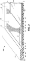
- Fig. 2 is a cross-sectional view of another inventive OLED module 110 using the flexible OLED panel 3 as the light source.
- OLED module 100 as shown in Figs. 1A-1D and OLED module 110 is that in this embodiment, the support 20 is rigid and flat as opposed to rigid and curved. Otherwise, all parts are the same.
- the backing plate 10 On the rigid and flat support 20 is the backing plate 10.
- OLED panel 3 Over the backing plate is located OLED panel 3 which has an OLED substrate 31 with an emissive area 32 surrounded by a non-emissive area 38. Note that the backing plate 10 extends past the end of the OLED substrate 31 of OLED panel 3 and is covered by the bezel 6.
- the first section (portion) 41 of the opaque liner Over the non-emissive area 38 of the OLED panel 3 is the first section (portion) 41 of the opaque liner.
- opaque liner 4 is arranged so that section 41, which is over the OLED substrate 31, does not significantly cover the emissive area 32 and extends over the non-emissive area 38 of the OLED panel 3 and which also is over the OLED substrate 31.
- a second section 42 of the opaque liner 4 extends past the edge of the OLED substrate 31 to come in contact with the backing plate 10 and is covered by the bezel 6. Note that portion 42 of the opaque liner is not over the OLED substrate 31.
- the bezel 6 covers only the second portion 42 of opaque liner 4 and the backing plate 10.
- the OLED substrate 31 is not located under the bezel 6.
- the bezel 6 is bonded to the flat and rigid support 20 with an adhesive at adhesive area 62. There is also an adhesive overflow area 63 within the bezel 6. Circuit board 34, covering 35, and optional adhesive layer 37 will be discussed in further figures.
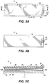
- Fig. 3A is a top view of the emissive side of one embodiment for a flexible bottom emitting (light is emitted through a transparent substrate) OLED lighting panel 3 useful for the OLED lighting module.
- On the surface of the emissive side there is an (optional) transmissive covering 35 through which light from the OLED light-generating unit is transmitted. Beneath the covering 35 is the OLED substrate 31, which is transparent.
- On the side of the OLED substrate 31 opposite from the covering 35 is the OLED light-emitting unit, which has an emissive area 32 surrounded by a non-emissive area 38.
- a circuit board 34 On the non-emitting side of the OLED light-emitting unit, there is a circuit board 34.
- the transmissive covering 35, OLED substrate 31, the light-generating OLED unit 32 / 38 and circuit board 34 all have approximately the same length and width dimensions.
- Circuit board 34 has two flat electrical connectors 141 and 142 (which together form a contact pad 14 for the OLED panel) that are separately connected to the two internal electrodes within the OLED light-generating unit and extend out from the emissive area 32 on an extension tab 36.
- the flat electrical connectors 141 and 142 of the circuit board 34 are located on the side of the circuit board 34 facing the non-emitting side of the OLED light-generating unit.
- the flat electrical connectors 141 and 142 on the extension tab 36 may be covered by an insulating material and not visible from the emissive side.
- Fig. 3B is a top view of the non-emissive side of the same OLED lighting panel 3 shown in Fig. 3A .
- the OLED panel contact pad 14 consisting of flat electrical connectors 141 and 142 on the extension tab 36 which is folded back so that the backside (the side opposite the flat electrical connectors) of the extension tab 36 is in contact with the backside of the circuit board 34.
- Fig. 3C is a cross-sectional view of OLED lighting panel 3 .
- Above the OLED substrate is the OLED light-emitting unit emissive area 32 (comprising a first electrode, intermediate organic layer(s) for light emission and a second electrode).
- the emitting portion 32 of the OLED light-emitting unit does not extend to the edge of the OLED substrate 31, thus creating surrounding non-emissive area 38.
- Above the OLED light-emitting unit emissive area is encapsulation 33.
- an optional adhesive layer 37 whose purpose, whenever present, is to affix the OLED light-emitting unit 32 and OLED substrate 31 to the overlying circuit board 34.
- electrical leads 143 and 144 that extend from the electrodes within the OLED light-emitting unit 32/38 through the encapsulation 33 to make contact with the flat connectors 141 and 142 of the circuit board 34.
- Flat electrical connectors 141 and 142 (which together form a contact pad 14 for the OLED panel) extend along the bottom side (i.e. the side facing the OLED light-emitting unit 32 ) of the circuit board 34 on extension tab 36 which is folded back upon itself.
- the area of the transmissive covering 35, the OLED substrate 31 and circuit board 34 are all the same and their outside edges correspond to each other (except for the extension tab 36 of the circuit board 34 ).
- Fig. 4 is a cross-sectional view of an OLED module 120 , similar to module 110 as shown in Fig. 2 , using the OLED lighting panel 3 , as shown in Figs. 3A-3D .
- a backing plate 10 located between the backside of the circuit board 34 and the support 20. In this embodiment, it has approximately the same area as the transmissive covering 35, the OLED substrate 31 and circuit board 34 (excluding the extension tab 36 ) except for any cut-outs.
- the outside edge of 10 generally corresponds to the others except where it is cut out to allow space for folded-over extension tab 36 on the back of the circuit board 34.
- Flat electrical connectors 12 run (within channels or cut-outs in backing plate 10 ; not visible in this view) from the panel contact pad 14 to the external wires 7 located in the center of the module.
- the extending portion 42 of the opaque liner 4 meets the support 20.
- the bezel 6 is located over the opaque liner section 42 and directly contacts the support 20.
- the OLED panel 3 is affixed to the support only by the extending portion of the second portion 42 of the opaque liner 4 that lies beneath the bezel 6. Note that the bezel does not cover any part of the OLED substrate 31.
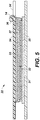
- Fig. 5 is a cross-sectional view of another embodiment of an OLED lighting panel 30 suitable for use in the OLED module of the invention.
- OLED lighting panel 30 is different from OLED lighting panel 3 is that both the transmissive covering 35 and circuit board 34 are longer in both length and width dimensions than the OLED substrate 31.
- the circuit board 34 has a cut-out for the extension tab 36 and contact pads 14 so that they remain in the same relative position to the emitting portion of the OLED. This creates overhanging portions of 35 below the OLED substrate 31 as well as overhanging portions of 34 above the OLED substrate 31.
- FIG. 5 shows these overhanging portions of 34 and 35 as extending in the same plane as the portions directly in contact with the OLED substrate 31 (for 35 ) or adhesive layer 37 /encapsulation 33 (for 34 ). If desired, the space between the overhanging portions may be filled with adhesive or other materials to protect the vertical edge of OLED substrate 31.
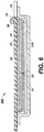
- Fig. 6 shows a cross-sectional view of an OLED lighting panel 300 which is another embodiment similar to 30 but where the transmissive covering 335 is sufficiently flexible that the overhanging portions comes into contact with circuit board 34 in the non-emitting areas of the OLED panel. If desired, any remaining space between the overhanging portions may be filled with adhesive or other materials to protect the vertical edge of OLED substrate 31.
- the circuit board 34 is shown as extending in the same plane as the portions directly in contact with the OLED substrate 31 while the extension of covering 335 is shown as bending to meet the circuit board 34.
- the covering 335 extends in the same plane while the circuit board 34 bends or the covering 335 and the circuit board 34 both bend to meet each other.
- Fig. 7 is a cross-sectional view of an OLED module 150 , similar to that shown in Figs. 2 and 4 , using the OLED lighting panel 300 , as shown in Fig. 6 .
- Flat electrical connectors 12 run from the panel contact pads 14 to the external wires 7 located in the center of the module.
- the bezel 6 is located over portions of the opaque liner 4, the covering 35, the circuit board 34 and the cover plate 10, all within the non-emitting area 38 of the OLED lighting panel 300 . All four of these structures extend past the edge of the OLED substrate 31. Only these extending portions are located under the bezel 6.
- the bezel does not cover any part of the OLED substrate 31.
- the bezel is in direct contact with the support 20.
- the module may contain more than two or more adjacent OLED lighting panel that all emit light in the same direction.
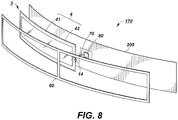
- One example 170 is shown in Fig. 8 .
- On the emissive side of the OLED panel 3 there is an opaque liner 4 with two portions 41 and 42.
- First portion 41 of the opaque liner is located over the OLED substrate of the OLED lighting panel 3 .
- Second portion 42 extends past the edges of the OLED substrate and therefore past the edges of OLED lighting panel 3.
- Second portion 42 of the opaque liner 4 is covered by bezel 60 and when assembled, the bezel 60 holds the OLED panel 3 to the support through section 42 of the opaque liner.
- the edge of the OLED panel contact pad 14 (on the non-emitting side of the panel) can be seen along with external wires 70 which extend through opening 80 in support 200.
- the two OLED panels would be arranged so that their contact pads would be orientated towards each other but not directly touching.
- the bezel 60 has a crossing section that covers and hides the adjoining edges of the two OLED panels.
- the OLED lighting module have external electrical connections accessible through an opening located in the middle of the backside of the module.
- OLED panels will have electrical contact pads located along one edge of the panel.
- at least one of the OLED panels will have electrical connections that extend from the panel contact pad on the edge of the panel to the center of the backside of the panel. For example, see Fig. 4 .
- this is not necessary since the contact pads located on the edge of at least one of the OLED panels will be located near the opening in the middle of the backside of the module. For example, see Fig. 8 .
- the support of the OLED module can be either rigid and flat or rigid and curved. It may be made of metal or plastic or other materials so long as it has sufficient mechanical strength. If metal, it can serve as a heat sink. It is preferred that the support is opaque, although in some designs it may have translucent or transparent sections. Typically, the support will be greater in both length and width than the OLED light panel.
- the support may be continuous without any openings under the OLED panel, or may have cut-outs or openings as desired. While the support will typically conform to the overall shape of the OLED lighting panel, this is not necessary and the support may have extensions or portions that do not conform to the shape of the OLED panel.
- the support may be part of the module surface or the support may be contained within another housing which serves as the outside surface of the module.
- the support may have provisions for attaching the module to a luminaire.
- the support should be no more than 1 mm thick and more desirably in the range of 0.05-0.75 mm thick. While the support would typically have constant thickness throughout, it may have sections that are thinner than others. While the support would typically form a single plane (either flat or curved), it may have sections that are out-of-plane (i.e. raised or indented) relative to others.
- the curve can be a simple regular curve or arc with no straight portions. However, it can also form more complex curves such as S-shaped or sine curves. It may have one or more straight portions joined by a curved section such as an inverted V or W shape.
- the emissive side of the OLED panel can be orientated along the outside or exterior side of the curve (away from the center point) or orientated along the inside or interior side of the curve (towards the center point).
- the curved support can be made of, for example, molded plastic, stamped metals or metals that retain their shape after bending such as annealed aluminum.
- the OLED panel lies upon and conforms to the shape of the support, whether planar or curved.
- a bezel covers the vertical sides and at least a portion of the front surface along the top edge. If the support is rigid, the bezel may be rigid or flexible. If the support is curved, the bezel should match the curvature of the support.
- the bezel may be made of the same material as the support or be made from a different material. It is desirable that the bezel match the support in appearance and material, although this is not necessary. While the bezel would typically have constant thickness throughout, it may have sections that are thinner or thicker than others.
- the bezel should not cover any part of the OLED substrate, but rather only by those portions of the opaque liner or parts of the OLED panel that extend past the outside edges of the OLED substrate. If there is only one extending portion under the bezel, it should be the second section of the opaque liner which is located on the emissive side of the OLED substrate. There can be more than one other extending portions under the bezel. In the case of two or more extending portions being under the bezel, there should be desirably at least one extended or overhanging portion that lies on one side of the OLED substrate and at least one extended portion that lies on the opposite side of the OLED substrate.
- the bezel should be relatively thin in width over the front surface of the module in order to provide a slick appearance.
- the bezel should be less than 10 mm wide (as measured from the interior edge of the bezel over the opaque liner to the outer edge) and more desirably 5 mm or less.
- the opaque liner located on the emissive side of the panel, extends past the outside edge of the OLED substrate and under the bezel.
- the bezel does not extend over the OLED substrate; it extends only over that portion of the opaque liner that extends past the edges of the OLED substrate.
- the backing plate located on the opposite side of the substrate from the opaque liner, can also extend past the outside edge of the OLED substrate and under the bezel, as shown in Fig. 7 .
- the OLED panel is held against the support by the bezel by the two extending portions of the opaque liner and the backing plate, each located on different sides of the OLED substrate. In this way, the module can be made very thin since the bezel does not have to cover the OLED substrate, which is one of the thickest parts of the OLED panel.
- the bezel may cover any of the following combinations of parts that extend past the outside edges of the OLED substrate: the opaque liner alone, the opaque liner + transmissive covering, the opaque liner + transmissive covering + circuit board, the opaque liner + transmissive covering + circuit board + backing plate, the opaque liner + circuit board, the opaque liner + circuit board + backing plate and the opaque liner + backing plate.
- the bezel is a separate part from the support.
- the module is assembled by attaching the bezel around the outside edges of the support so that part of the bezel covers at least that part of the opaque liner not over the OLED substrate to affix the OLED panel within the module.
- the bezel may be attached to the support by adhesives or by mechanical means (i.e. screws, pins, interlocking features such as snaps, etc.).
- the bezel is an integral part of the support and there is a slot between the upper surface of the support and the bottom of a retaining edge of the bezel.
- the module is then assembled by sliding the extensions of the OLED lighting panel along the length of the slot. After the OLED panel is inserted and in the desired position, the slot is then closed to complete the assembly.
- the OLED panel is only held against the support by the bezel, which does not hold the OLED substrate directly, but rather by the extending portions of the opaque liner (and, in some embodiments, along with other extending portions).
- the panel is additionally held against the support by adhesives as well as the bezel. There may be one point of attachment, multiple points of attachment or continuous attachment. Desirably, the OLED lighting panel is only contained and held in place by compression or pinning between the support and the bezel so that the OLED is free to move due to thermal expansion or contraction.
- the bezel runs along the outside edges of the module, in some designs the bezel may also have cross-pieces that run over the emitting surface. These may be purely decorative, hide non-emitting joints or may serve to stiffen the module or provide physical protection to the front surface.
- a curved support, bezel or module (with or without the OLED panel) could also be prepared from a thermoplastic material which is initially flat, heated and molded to into the desired curved shape, and which retains the desired shape upon cooling.
- they could be formed from a shape-memory alloy which is an alloy that "remembers" its original shape and that when deformed returns to its pre-deformed shape when heated.
- two OLED panels may be assembled back-to-back so that there is two-sided emission.
- the support can either be at least partly transparent or have openings to allow emission in both top and bottom directions.
- an OLED panel with two-sided emission (that is, the opposite side of the panel is also light emissive) can also be employed.
- the OLED panel with two-sided emission may be transparent or translucent.
- the opaque liner Since the opaque liner is located on the emitting side of the OLED lighting panel, the opaque liner should have an open area roughly corresponding to the emitting area of the OLED panel for light emission.
- the opaque liner should cover the non-emitting areas on the emitting surface of the OLED lighting panel which generally surrounds the light-emitting area.
- the opaque liner is attached to the surface of the OLED panel by adhesives.
- the visible width (that is, the part not under the bezel) of the opaque liner should be less than 15 mm and more desirably less than 10 mm.
- the opaque liner should be flexible.
- the opaque liner should be thin; desirably, the opaque liner should be no more than 0.5 mm thick and more desirably in the range of 0.01-0.2 mm thick, which includes any adhesive layer if present.
- the opaque liner is formed of one continuous piece, there are at least two sections of the opaque liner: a first section that covers (located over) the OLED substrate of the OLED panel and a second section that extends or overhangs past the outside edges of the OLED substrate so that there is no OLED substrate below the second section.
- Some suitable materials for the opaque liner would be plastic or polymeric films, glass or metal foils, or woven or non-woven fabrics. It may be made of multiple layers.
- the backing plate can be flexible, between the circuit board of the OLED lighting panel and the support.
- the backing plate extends past the edges of the OLED substrate and under the bezel.
- the outside edges of the backing plate correspond to or exceed the outside edges of the circuit board.
- the outside edges of the backing plate are entirely within the outside edges of the circuit board.
- the backing plate may be one solid and continuous piece or may have cut-outs to allow space for the extension tab, wiring that runs along the back of the panel or for the contact pads of the OLED panel.
- the backing plate may have channels or inserts to allow space for the wiring.
- the backing plate may be non-conductive. One suitable material would be Kapton.
- the backing plate may be metallic and serve as a heat sink. Desirably, the backing plate should be no more than 0.5 mm thick and more desirably in the range of 0.001-0.2 mm thick.
- the backing plate may be attached to either the circuit board of the OLED panel or the support of the module or both by adhesives. Desirably, the backing plate is opaque although it may be translucent or transparent to allow for two-sided emission.
- the OLED lighting panel for use in the module will typically have its electrical contact pads for supplying power to the internal electrodes in the non-emitting areas of the panel.
- the contact pads are generally either located on the front side along the side of the emitting areas or along the edge of the back side of the panel. Both types are suitable for use in the module.
- External electricals wires will supply power to the contact pads of the OLED panel within the module. These wires can be attached to the contact pads by any known method such as soldering, conductive glue, ACF (Anisotropic Conductive Film), etc. Because it is desired that the module be as thin as possible, flat wires should be used within the module.
- the external wires may pass through an opening anywhere in the module. For example, the opening may be along one edge (for example, between the bezel and support or directly through the side of the bezel), along the front edge (for example, through the top of the bezel, through the opaque liner or both) or anywhere on the back of the module through the support. Most desirably, the opening is located in the geometric center of the backside of the support.
- the flat wires within the module made be connected to a separate pass-through circuit board at the opening so that round wires can be used outside the module.
- the opening may be sealed after assembly; for example, by silicon sealant.
- the OLED module may have provisions or structures that enable mechanical attachment to a luminaire. Such attachment points may be anywhere on or across the device. There can be one attachment point or multiple attachment points. Ideally, the attachment point may be at a balance point of the module although this is not necessary.
- the mechanical attachment feature may also provide electrical connection or may be separate from the electrical connection.
- the mechanical attachment feature may be permanent (for example, a solder joint between the module and a supporting structure), flexible or adjustable (for example, a ball and socket joint) or temporary and removable (for example, a detachable tab and socket mechanism).
- Suitable OLED lighting panels are any that can be used for general lighting applications. However, the panel may be modified for use in specific applications. For example, it may be fitted with a lens to concentrate the emitted light in order to act as highlighting or it may be fitted with filters to adjust the color temperature of the emitted light.
- the OLED panel desirably has a flexible transmissive cover on its emitting surface. It may have the same area as the emissive area of the OLED, or the same area as the OLED substrate and cover both the emitting and non-emitting areas. It may be larger than the OLED substrate.
- the transmissive cover may be a flexible optically clear protective film or provide light management functions such as diffusion or light scatter, color filter or a polarization filter.
- the flexible transmissive cover may be a light management film or unit that serves a number of purposes and may be composed of multiple layers. Its primary purpose is to increase the amount of light scatter of the light being transmitted through the OLED substrate, thus improving light distribution from the device and improving overall efficiency.
- the flexible light management unit will have a light scattering medium located either on the surface or within a flexible polymeric or glass substrate or the flexible substrate will contain physical structures (for examples, bumps or projections of various shapes) that cause light scattering.
- the flexible light management unit may be part of the same OLED substrate as the OLED unit. In other cases, it may be a separate unit that is applied to the light-emitting surface of the OLED unit / substrate using an optically clear adhesive. In addition to its light management function, it will also help to protect the surface of the device from damage. In embodiments where the light management unit is larger in area than the OLED substrate so there is a portion that overhangs the OLED substrate, the overhanging portions may extend under the bezel and help to hold the OLED lighting panel within the module.
- the OLED substrate is flexible and can be made of flexible glass, polymeric materials or metals. Flexible glass is most desired. Generally speaking, it will be flat with a uniform thickness. For bottom emitting OLEDs, the substrate should be transparent. For top emitting OLEDs, the substrate may be opaque or transparent (allowing for two-sided emission) as desired. The top surface of the OLED substrate is that facing the OLED light-generating unit. Since the substrate will be part of the overall encapsulation for the OLED, it should be sufficiently impervious to air and water so that the OLED will have desired lifetime.
- the OLED substrate may have various types of subbing layers which may be patterned or unpatterned and can be either on the top or bottom surfaces.
- an OLED light-emitting unit with a first electrode, electroluminescent layer(s), and second electrode, all fully covered by encapsulation to prevent contact with air and water.
- a first electrode that covers the top surface of the substrate and desirably completely covers the top surface of the substrate.
- the first electrode can be an anode or a cathode and can be transparent, opaque or semitransparent. Desirably, the first electrode is a transparent anode and the OLED device is a bottom emitter.
- the transparent first electrode should transmit as much light as possible, preferably having a transmittance of at least 70% or more desirably at least 80%. However, in some applications (i.e.
- the transparent first electrode may only be semitransparent and have partial reflectivity. While the first transparent electrode may be made of any conductive materials, metal oxides such as ITO or AZO or thin layers of metals such as Ag are preferable. In some cases, there may be an auxiliary electrode to help distribute charge more uniformly across the full plane of the transparent electrode.
- the electroluminescent layer of the OLED light-generating unit is located between the electrodes.
- the electroluminescent layer may include multiple layers where at least one organic layer will be electroluminescent. Formulations and layers appropriate for OLED type light emission are well known and can be used as desired.
- the organic layers may be small molecule or polymeric.
- the organic layers may be deposited by any known method including vapor deposition, solution coating, ink-jet techniques, spraying and the like.
- the organic layers may be patterned.
- Inorganic electroluminescent materials such as quantum dots could also be used for light emission. Because such formulations also include organic materials, the use of inorganic electroluminescent materials can be considered as an OLED for the purpose of the invention.
- a second electrode Over the electroluminescent layer, there is a second electrode. It may be an anode or a cathode; preferably a cathode.
- the second electrode may be transparent or opaque, preferably opaque. If transparent, it is desirably composed of conductive transparent metal oxides such as ITO or thin layers of metals such as Ag. If opaque, it is desirably composed of a thicker layer of metal or metal alloy such as Al, Ag, Mg/Al, Mg/Ag and the like.
- the second electrode may be deposited by any known technique.
- a protective organic layer Over the second electrode, there may optionally be a protective organic layer, protective inorganic layer, or a combination of both. This is to prevent damage to the second electrode and underlying organic layers during encapsulation.
- the OLED light-emitting unit is fully encapsulated.
- the encapsulation is provided on one surface by the OLED substrate.
- the sides and top of the OLED unit can be encapsulated by a flexible impervious cover that is affixed to the substrate to seal the OLED unit.
- the encapsulation of the sides and top of the OLED unit is provided by thin-film encapsulation.
- Thin-film encapsulation typically includes multiple (for example, 3 or more) alternating layers of inorganic and organic materials.
- thin-film encapsulation may also comprise a two-layer barrier system of an adhesive layer with water adsorbing getter particles covered with an impermeable layer or film such as a thin metal foil or a plastic barrier film.
- There are electrically conductive extensions of the first and second electrodes that will extend through and beyond the encapsulation and form contact pads in the non-encapsulated regions for external electrical connection.
- adhesive materials and/or protective layers to fasten the OLED unit / substrate to an overlying circuit board.
- adhesive materials should be flexible.
- suitable adhesive materials would be double sided adhesive tape or liquid adhesive, which may be applied by spraying, brushing, rolling, lamination or similar methods.
- metal foil present to help serve as a heat sink as well to prevent damage to the OLED unit during manufacture.
- Inorganic or polymeric layers may also be used as protective layers. The metal foil or other protective layers may be present between adhesive layers. If the adhesive or protective layers are electrically conductive, they must be arranged not to come into contact with either the contact pads of the OLED unit or the flat electrical connectors of the circuit board or any connectors between the two.
- the circuit board is on the opposite side of the OLED unit from the OLED substrate.
- the main body of the circuit board desirably has the same or greater area than the emissive area of the OLED unit, even though it may be located on the opposite side of the emissive side of the OLED substrate.
- the circuit board can provide protection against damage to the underlying OLED unit as well as acting as a heat sink.
- the circuit board can completely overlap and could have an area the same as or greater than that of the OLED substrate.
- the overhanging portions may be used to attach the panel to a mounting or surface.
- the circuit board can have non-printed electrical connections.
- the circuit board is smaller in area than the emissive area of the OLED and can be located along the side of the OLED substrate or can form a frame around the outside edge of the OLED substrate, which may or may not overhang the OLED substrate.
- the flexible printed circuit board is made of non-electrically conductive plastic or polymeric materials. It may be composed of two or more layers and these layers can be made of different materials. At a minimum, it has at least two flat electrical connectors on one surface of the circuit board and the extension tab. There may be other electrical control (such as transistors) or power (such as resistors) related features on either surface of the circuit board or on the extension tab. Desirably, it is opaque but may be translucent or transparent for two-sided emission.
- the flat electrical connections on the flexible printed circuit board are made of electrically conductive metals such as Al, Cu, Sn. They should have sufficient flexibility to be able to bend without breaking.
- the surface of the circuit board with the flat electrical connectors faces the adhesive materials and/or protective layers (if present) and the OLED unit. Since the flat electrical connectors may be bent in some embodiments, the flat electrical connectors may contain stress-relieving features that allow the bending without cracking or breaking.
- the electrical contact between the flat electrical connectors of the circuit board to the contact pads on the OLED substrate may be direct when the OLED substrate and circuit board are placed face-to-face.
- electrically conductive glue or adhesive or appropriately sized and shaped ACF may be used to make electrical contact between them.
- other methods for making electrical contact can be used.
- the flat electrical connectors on the circuit board of the OLED panel connect to electrical contact pads for the panel, which are typically located in non-emitting areas on either the front or back of the panel. This allows for a modular approach where external wires may be connected to the panel in various ways as needed.
Description
- This application claims the benefit of
U.S. Provisional Application No. 62/615,129, filed January 9, 2018 PCT/EP2019/050407 - OLED technology offers many advantages for general lighting purposes. OLED devices are efficient in terms of light output for power consumed. They are low voltage which helps avoid potential electrical shocks, less prone to sparking in potentially explosive environments, and they reduce loads in the supporting electrical system. The spectrum of emitted light can be varied using appropriate internal designs. They produce little or no UV or IR light. They are instant on; that is, they emit light immediately whenever electrical power is supplied. OLED light sources are inherently flat area light sources. They offer several advantages over LED light sources. OLED devices can be made even thinner (for example, less than 1 mm thick) and they produce less heat under normal operating conditions. However, OLED lifetimes can be an issue. Both LED and OLED devices can be made on flexible or curved supports although OLED is preferred for these types of applications.
- Generally speaking, an OLED device used for lighting purposes would include an OLED lighting panel as the light source. An OLED panel would have at least three parts: a substrate, an OLED light-emitting unit upon the substrate, and electrical connections which provide power to the internal OLED electrodes from an external source. An OLED light-emitting unit would have at least one organic electroluminescent layer between two electrodes and would be encapsulated to protect the electroluminescent layer(s) from air and/or water. Typically, the OLED panel would have emissive areas surrounded by non-emitting borders. Electrode contact pads, which are connected to the internal electrodes, are often located in these non-emitting border areas on the same face of the substrate as the electroluminescent layers or on the non-emitting areas on the backside. OLED light-emitting units can be prepared on either rigid or flexible substrates. While both can be very thin, flexible substrates are advantaged since they can be used in curved or bent designs as well as in rigid (flat or bent) applications when further supported by an inflexible or rigid housing or mounting.
- OLED lighting panels can be used as a light source in a luminaire or lamp. Luminaires are used in many ways; for example, overhead lighting such as chandeliers, wall lighting such as sconces or table lighting such as desk lamps. In order to minimize production costs, it would be desirable to incorporate the OLED lighting panel in a single modular design that can be used in many different styles of luminaires. An OLED lighting module would be a set of standardized parts or independent units that can be used to construct a more complex structure using an OLED lighting panel as the light source.
- Generally speaking, an OLED module would have at least three parts: a bottom housing or support, an OLED lighting panel in the middle and a top housing or bezel with an opening for light emission. The bottom housing may also have an opening for light emission as well if using an OLED panel that emits light from two sides or if two OLED light panels are used back-to-back. To maintain a slick and neat appearance, the external electrical connections are usually hidden within the module and external electrical connections are through a standardized non-permanent connection point such as an electrical jack or plug. This is consistent with a modular design. The lighting module should also have some allowance for mechanical support and/or attachment to the body of the luminaire.
- It would be desirable to design a module using an OLED lighting panel where the module takes full advantage of the thinness and flexibility of the OLED lighting panel. Thus, the module could be flexible. However, since in some applications a flexible module is not desirable, the module could be rigid and flat and still emphasize the thinness of the OLED panel. In other applications, the lighting module could be rigid and curved in order to emphasize the flexibility of the OLED lighting panel as well. Such designs would have aesthetic appeal in many applications.
- The use of rigid curved lighting modules in a luminaire is known, including the use of flexible OLED lighting panels mounted on a rigid and curved support. For example,
US9723686 US2016/0320027 ,US20160061422 andJP2016225209 JP2007-005226 - In a luminaire with a modular design, an OLED panel needs to be permanently mounted on the housing or support within the module. Since the OLED panels create some degree of heat, they must be mounted in a way that prevents thermal buckling. For example, attaching the OLED panel only on both ends (without any attachment in the middle of the panel) would be desirable for ease of mounting, but could allow for buckling during extended operation. Moreover, any end-only attachment means would have to be fairly thick in order to provide the degree of robustness required so that the panel doesn't become loose.
- Another way to attach an OLED lighting panel to a housing is to use a bezel that covers the ends and sides of the OLED lighting panel. A bezel is generally a grooved ring or partial cover that holds the lighting panel in position. It would fit over the surface of the panel and be attached to either the lighting panel or support or both. The use of such bezels is known; for example, see
US7961456 ,US7960913 ,US8885116 ,US7786559 ,US8471462 , andEP2661778 . However, since these bezels are designed in part to provide shock protection to the panels, they are robust and do not allow for a module that is as thin as possible. - While the support and/or bezel can act to some degree as a heat sink, they may not provide enough thermal protection to prevent thermal buckling or degradation of the OLED panel. This problem can be solved by adding an additional heat sink structure, but this will only add additional thickness to the module.
- Electrical power needs to be delivered to the OLED panel within the module. OLED lighting panels typically have electrical contact pads along the non-emitting sides of the emissive area of the panel on the same side of the OLED substrate or on its backside. For some applications, it would be desirable for aesthetic reasons to have the electrical connections made in the center of the backside of the module (if curved, ideally at the midpoint of the curvature). In such modules using only a single OLED lighting panel or an odd number of panels, it can be difficult to maintain the thinness of the module(s) since the electrical connections from at least one of the OLED panels within the module must run from the external contact pads of the OLED light-emitting unit to the middle of the backside of the module. For such modules using two OLED panels or an even number of panels, the electrical connections can be made along one of the edges of the panels, although the electrical connection still needs to run through the module to the backside.
- There is a desire for a lighting module for use in a luminaire or other general lighting fixtures where the lighting module uses an OLED lighting panel while maintaining as thin a profile as possible. In addition, it would be desirable that in order to maximize the amount of emitted light from the module, the front housing / bezel should not cover any of the emitting portions of the OLED lighting panel. While the bezel could cover all of the non-emitting portions of the OLED lighting panel, having the bezel cover the panel directly could add thickness to the overall module and leads to a situation where the surface of the OLED lighting panel is significantly below the top surface of the bezel, giving a noticeable indented or set-back appearance that may not be desirable. Moreover, having the bezel cover all of the non-emitting portions of the OLED panel might lead to impression of having a relative wide frame which would distract from a thin and slick appearance.
-
US 2010/327737 A1 concerns an electro-optical device that includes a display panel having an electro-optical layer, a first resin film stacked on the display panel to cover a first surface on the side of a display area of the display panel, and a second resin film stacked on the display panel to cover a second surface opposite the first surface, and at least one reinforcing member disposed on at least one of the first resin film and the second resin film. -
KR 2009 0093058 A -
US 2009/207560 A1 concerns an electronic device having an impact resistance property. The electronic device includes an OLED display device and a housing receiving the OLED display device. The OLED display device includes a panel assembly on which a plurality of OLEDs are formed and a printed circuit board electrically connected to the panel assembly. The housing includes a reinforcing housing having an impact absorption ability and defining first and second spaces, an upper housing disposed within the first space and physically coupled to the reinforcing housing, and a lower housing disposed within the second space and physically coupled to the reinforcing housing. -
US 9727080 B2 -
WO 2017/147373 A1 concerns a flat and detachable electrical connection system between a flat lighting module and a lampholder. The flat lighting module comprises a lighting panel, control circuitry for controlling the lighting panel, and electrical contact pads connected to the control circuitry, all supported at least in part by a mechanical support plate; the mechanical support plate being at least partially enclosed in a housing with a provision or opening so that light can be emitted from the lighting panel; and where the mechanical support plate includes a male mechanical support connector section that extends out from the mechanical support plate in the same plane as the thickness of the lighting module; and where the male mechanical support connector section includes means for non-permanent locking or latching of the lighting module to the lampholder. -
US 2014/247584 A1 concerns a light-emitting device including a planar light-emitting unit having a light-emitting surface and a non-light-emitting surface, a planar solar power generator having a light-receiving surface and a non-light-receiving surface, and a rechargeable battery. The light-emitting unit and the solar power generator are arranged so that the non-light-emitting surface and the non-light-receiving surface face each other, thereby forming a light-electricity converter. - The present invention concerns an OLED lighting module according to
claim 1. Further aspects of the present invention are defined in the dependent claims. - A very thin OLED lighting module is enabled by attaching an OLED lighting panel to a support using a bezel located over a portion of an opaque liner on the emitting side of the OLED lighting panel that overlaps the edges of the OLED substrate. By covering only those portions of an opaque liner that extend past the edges of the OLED substrate and not the OLED substrate itself, the bezel can be made much thinner and yet still affix the panel to the module support.
- This can be accomplished by an OLED lighting module comprising: a support; one or more OLED lighting panel(s) on the support, wherein each OLED panel has an emissive side with emissive and non-emissive areas and an opposite side, and comprises an OLED substrate, an encapsulated OLED light-generating unit on the OLED substrate and a circuit board containing flat electrical connectors, the circuit board being located between the OLED light-generating unit and the support; an opaque liner on the emissive side of the OLED panel, the opaque liner having two sections: a first section that covers at least part of the non-emitting areas over the OLED substrate and a second section that extends past the edges of the OLED substrate; and an opaque bezel in contact with the support, the opaque bezel covering at least part of the second section of the opaque liner but not the first section of the opaque liner.
- In some embodiments, the support (metal or plastic) is rigid and curved and the opaque bezel can either be rigid and curved or flexible. The bezel lies along and hides the thin vertical edges of the OLED panel. The OLED lighting panel and its components can be flexible. The OLED panel can be bottom-emitting. The opposite side of the OLED panel can be non-emitting or emitting with emissive and non-emissive areas.
- There can be a transmissive covering, which can be flexible, over the emissive areas of the OLED panel. In some embodiments, the transmissive covering is a light-management film with portions that extend past the edges of the OLED substrate; wherein the light-management film is covered in part by the first section of the opaque liner, and where the extended portions of the light-management film are covered at least in part by the second section of the opaque liner and at least in part by the bezel. In some embodiments, the outside edges of the opaque liner correspond to or exceed the outside edges of the transmissive covering. In other embodiments, the outside edges of the opaque liner are entirely within the outside edges of the transmissive covering.
- In some embodiments, a portion of the circuit board extends past the edges of the OLED substrate.
- In some embodiments, there is a backing plate located between the circuit board and the support. In some cases, a portion of the backing plate extends past the edges of the OLED substrate.
- In addition to the opaque liner, the bezel may additionally cover the extending portions of the transmissive covering, the circuit board and backing plate individually or in any combination. In one preferred embodiment, the bezel covers the extending portions of the opaque liner and backing plate. In another preferred embodiment, the bezel covers the extending portions of the opaque liner, the transmissive covering, the circuit board and backing plate.
- The flat electrical connectors of the circuit board are in electrical contact with the internal electrodes of the OLED. The flat connectors are located on the surface of the circuit board facing the OLED. The flat electrical connectors on the circuit board of the OLED panel connect to electrical contact pads for the panel, which are located in non-emitting areas on either the front or back of the panel.
- OLED lighting modules can be prepared that are very thin but yet are robust. This allows for a stylish and sophisticated appearance different from other types of lighting panels (i.e. LED) or from known lighting modules. The lighting modules can be used in flexible, rigid and flat, or rigid and curved applications. If the opaque liner is made of a flexible material, it can absorb some of the external forces put on the OLED panel. Moreover, using a flexible opaque liner minimizes problems due to differences in thermal expansion between the materials of the lighting module. Luminaires using OLED lighting modules can be manufactured with reduced cost and complexity.
-
-
Fig. 1A is a top view of one side of a curved OLED module.Fig. 1B is an exploded view of the same OLED module in the same direction.Fig. 1C is a top view of the other side of the same OLED module as inFigs. 1A and 1B .Fig. 1D is an exploded view of the same OLED module in the same direction asFig. 1C . -
Fig. 2 is a cross-sectional view of a flat OLED module showing the details of the bezel, the OLED lighting panel and module support. -
Fig. 3A is a top view of the emissive side of an OLED lighting panel.Fig. 3B is a top view of the non-emissive side.Fig. 3C is a cross-section view of the same OLED lighting panel. -
Fig. 4 is a cross-sectional view of an OLED lighting module using the OLED lighting panel shown inFigs. 3A-3C . -
Fig. 5 is a cross-sectional view of another embodiment of an OLED lighting panel. -
Fig. 6 is a cross-sectional view of a variation of the embodiment of the OLED lighting panel shown inFig. 5 . -
Fig. 7 is a cross-sectional view of an OLED lighting module using the OLED panel shown inFig. 6 . -
Fig. 8 is an exploded view of the emissive side of an OLED module that uses two adjacent OLED lighting panels. - The Figures are not drawn to scale.
- In the following, the example module and panel structures are all shown as being rectangular in shape and length and so, references are made to length and width. However, the modules and panels are not limited to any particular shape and so, may be square, circular, oval, triangular or an irregular shape. In any case, the module, panel and certain internal features will all have outside edges and so, for shapes other than square or rectangular, corresponding dimensions (for example, radius for circular panels) should be applied. Rectangular or square panels are preferred. In addition, although the examples refer to using an OLED as a specific example of a light-emitting unit, any kind of light-emitting unit containing organic material would be generally useful. By one structure "covering" or "covers" another structure, it is meant that one lies over (relative to the bottom) either entirely or partially.
- An OLED module of the invention comprises at a minimum, a support, an OLED lighting panel, and a bezel. The OLED lighting panel used in the OLED module comprises at a minimum, an OLED substrate, an encapsulated OLED light-generating unit on the OLED substrate and a circuit board. The OLED panel is retained to the support by a bezel which covers at least an overlapping or free-hanging portion of an opaque liner which also covers a non-emissive (also called non-emitting) portion of the OLED panel.
- It is desirable that the overall thickness of the OLED module should be no more than 5 mm, preferably less than 3 mm and most desirably less than 2 mm.
-
Fig. 1A is a view of the emissive side of one embodiment of theOLED module 100 of the invention. In this embodiment, there is a rigid andcurved support 2 on which there is a flexibleOLED lighting panel 3 which conforms to the shape of the support. The curve of thesupport 2 forms a regular arc where the emissive surface of theOLED lighting panel 3 is on the outside side of the arc. Surrounding the emissive area of theOLED lighting panel 3 and covering the non-emissive area is anopaque liner 4, which has two connected sections. Afirst portion 41 of theopaque liner 4 lies over at least part of the non-emitting border of the OLED panel which is supported by the OLED substrate. There is asecond portion 42 of the opaque liner that extends past the outside edges of the OLED substrate. These two different portions or sections of theopaque liner 4 cover areas with different heights and so, there will be a visible change in height betweensections opaque liner 4 as indicated by 5. The outside edges of the opaque liner 4 (specifically thesecond portion 42 of the opaque liner that extends past the OLED substrate) are covered by abezel 6, which runs along the top edge of the module as well as along its side edges. The bezel does not cover any of the first portion of 41 of the opaque liner. There is a thickening 61 of the bezel in one area. This thickening can be part of or cover a point of attachment of the module. This view also showsexternal wires 7 that originate from the opposite side of themodule 100. -
Fig. 1B is an exploded view ofOLED module 100 as shown inFig. 1A . There is abacking plate 10 between the non-emissive side of theOLED panel 3 and the rigid andcurved support 2. On the non-emitting side of theOLED panel 3, the ends of theinternal wire connectors 12 can be seen. In this embodiment, an opening orwiring port 8 is located in the center (the midpoint of the length and width) of the module on its back. -
Fig 1C is a view of the non-emissive side of theOLED module 100. This view is of the inside curve of the arc. Shown is the rigid andcurved support 2 withexternal wires 7 extending from theopening 8. Theexternal wires 7 supply power from an external source via the flatelectrical connectors 12 to thecontact pads 14 of the OLED lighting panel within the module. -
Fig. 1D is an exploded view ofOLED module 100 as shown inFig. 1C . In this view,panel contact pads 14, located on the back (non-emitting side) ofOLED panel 3, can be seen. In the assembled module, thepanel contact pads 14 are electrically connected to thewire connectors 12. Thewire connectors 12 run from thecontact pads 14 to theexternal wires 7 at theopening 8 and run between the circuit board, which in this embodiment is on the non-emissive side ofOLED panel 3, and the front of the support between cut-outs in thebacking plate 10. -
Fig. 2 is a cross-sectional view of anotherinventive OLED module 110 using theflexible OLED panel 3 as the light source. The only difference betweenOLED module 100 as shown inFigs. 1A-1D andOLED module 110 is that in this embodiment, thesupport 20 is rigid and flat as opposed to rigid and curved. Otherwise, all parts are the same. On the rigid andflat support 20 is thebacking plate 10. Over the backing plate is locatedOLED panel 3 which has anOLED substrate 31 with anemissive area 32 surrounded by anon-emissive area 38. Note that thebacking plate 10 extends past the end of theOLED substrate 31 ofOLED panel 3 and is covered by thebezel 6. Over thenon-emissive area 38 of theOLED panel 3 is the first section (portion) 41 of the opaque liner. Note thatopaque liner 4 is arranged so thatsection 41, which is over theOLED substrate 31, does not significantly cover theemissive area 32 and extends over thenon-emissive area 38 of theOLED panel 3 and which also is over theOLED substrate 31. Asecond section 42 of theopaque liner 4 extends past the edge of theOLED substrate 31 to come in contact with thebacking plate 10 and is covered by thebezel 6. Note thatportion 42 of the opaque liner is not over theOLED substrate 31. There is a relative change in the overall thickness of the package past of the edge of theOLED substrate 31 where theopaque liner 42 meets thebacking plate 10. This is indicated by 5. Note that in this embodiment, thebezel 6 covers only thesecond portion 42 ofopaque liner 4 and thebacking plate 10. TheOLED substrate 31 is not located under thebezel 6. In this embodiment, thebezel 6 is bonded to the flat andrigid support 20 with an adhesive atadhesive area 62. There is also anadhesive overflow area 63 within thebezel 6.Circuit board 34, covering 35, and optionaladhesive layer 37 will be discussed in further figures. -
Fig. 3A is a top view of the emissive side of one embodiment for a flexible bottom emitting (light is emitted through a transparent substrate)OLED lighting panel 3 useful for the OLED lighting module. On the surface of the emissive side, there is an (optional) transmissive covering 35 through which light from the OLED light-generating unit is transmitted. Beneath the covering 35 is theOLED substrate 31, which is transparent. On the side of theOLED substrate 31 opposite from the covering 35 is the OLED light-emitting unit, which has anemissive area 32 surrounded by anon-emissive area 38. On the non-emitting side of the OLED light-emitting unit, there is acircuit board 34. In this example, the transmissive covering 35,OLED substrate 31, the light-generatingOLED unit 32 / 38 andcircuit board 34 all have approximately the same length and width dimensions.Circuit board 34 has two flatelectrical connectors 141 and 142 (which together form acontact pad 14 for the OLED panel) that are separately connected to the two internal electrodes within the OLED light-generating unit and extend out from theemissive area 32 on anextension tab 36. The flatelectrical connectors circuit board 34 are located on the side of thecircuit board 34 facing the non-emitting side of the OLED light-generating unit. In other embodiments, the flatelectrical connectors extension tab 36 may be covered by an insulating material and not visible from the emissive side. -
Fig. 3B is a top view of the non-emissive side of the sameOLED lighting panel 3 shown inFig. 3A . On the backside of thecircuit board 34 is located the OLEDpanel contact pad 14 consisting of flatelectrical connectors extension tab 36 which is folded back so that the backside (the side opposite the flat electrical connectors) of theextension tab 36 is in contact with the backside of thecircuit board 34. -
Fig. 3C is a cross-sectional view ofOLED lighting panel 3. On the surface from which light is emitted (as indicated by the arrow), there is atransmissive covering 35. Above this, there is theOLED substrate 31. Above the OLED substrate is the OLED light-emitting unit emissive area 32 (comprising a first electrode, intermediate organic layer(s) for light emission and a second electrode). The emittingportion 32 of the OLED light-emitting unit does not extend to the edge of theOLED substrate 31, thus creating surroundingnon-emissive area 38. Above the OLED light-emitting unit emissive area isencapsulation 33. Above that, there is anoptional adhesive layer 37 whose purpose, whenever present, is to affix the OLED light-emittingunit 32 andOLED substrate 31 to theoverlying circuit board 34. There areelectrical leads unit 32/38 through theencapsulation 33 to make contact with theflat connectors circuit board 34. Flatelectrical connectors 141 and 142 (which together form acontact pad 14 for the OLED panel) extend along the bottom side (i.e. the side facing the OLED light-emitting unit 32) of thecircuit board 34 onextension tab 36 which is folded back upon itself. This creates OLEDpanel contact pad 14 on the backside (non-emitting) of theOLED panel 3 . In this embodiment, the area of the transmissive covering 35, theOLED substrate 31 andcircuit board 34 are all the same and their outside edges correspond to each other (except for theextension tab 36 of the circuit board 34). -
Fig. 4 is a cross-sectional view of anOLED module 120, similar tomodule 110 as shown inFig. 2 , using theOLED lighting panel 3, as shown inFigs. 3A-3D . There is abacking plate 10 located between the backside of thecircuit board 34 and thesupport 20. In this embodiment, it has approximately the same area as the transmissive covering 35, theOLED substrate 31 and circuit board 34 (excluding the extension tab 36) except for any cut-outs. The outside edge of 10 generally corresponds to the others except where it is cut out to allow space for folded-overextension tab 36 on the back of thecircuit board 34. Flatelectrical connectors 12 run (within channels or cut-outs inbacking plate 10; not visible in this view) from thepanel contact pad 14 to theexternal wires 7 located in the center of the module. There is afirst portion 41 of theopaque liner 4 over thenon-emitting portions 38 of theOLED panel 3 on top of transmissive covering 35, and asecond portion 42 of theopaque liner 4 has that extends past the outside edges of theOLED substrate 31. In this embodiment, the extendingportion 42 of theopaque liner 4 meets thesupport 20. Thebezel 6 is located over theopaque liner section 42 and directly contacts thesupport 20. Thus, in this embodiment, theOLED panel 3 is affixed to the support only by the extending portion of thesecond portion 42 of theopaque liner 4 that lies beneath thebezel 6. Note that the bezel does not cover any part of theOLED substrate 31. -
Fig. 5 is a cross-sectional view of another embodiment of anOLED lighting panel 30 suitable for use in the OLED module of the invention.OLED lighting panel 30 is different fromOLED lighting panel 3 is that both the transmissive covering 35 andcircuit board 34 are longer in both length and width dimensions than theOLED substrate 31. Thecircuit board 34 has a cut-out for theextension tab 36 andcontact pads 14 so that they remain in the same relative position to the emitting portion of the OLED. This creates overhanging portions of 35 below theOLED substrate 31 as well as overhanging portions of 34 above theOLED substrate 31.Fig. 5 shows these overhanging portions of 34 and 35 as extending in the same plane as the portions directly in contact with the OLED substrate 31 (for 35) oradhesive layer 37/encapsulation 33 (for 34). If desired, the space between the overhanging portions may be filled with adhesive or other materials to protect the vertical edge ofOLED substrate 31. -
Fig. 6 shows a cross-sectional view of anOLED lighting panel 300 which is another embodiment similar to 30 but where the transmissive covering 335 is sufficiently flexible that the overhanging portions comes into contact withcircuit board 34 in the non-emitting areas of the OLED panel. If desired, any remaining space between the overhanging portions may be filled with adhesive or other materials to protect the vertical edge ofOLED substrate 31. In this illustration, thecircuit board 34 is shown as extending in the same plane as the portions directly in contact with theOLED substrate 31 while the extension of covering 335 is shown as bending to meet thecircuit board 34. However, it is also possible that the covering 335 extends in the same plane while thecircuit board 34 bends or the covering 335 and thecircuit board 34 both bend to meet each other. -
Fig. 7 is a cross-sectional view of anOLED module 150, similar to that shown inFigs. 2 and4 , using theOLED lighting panel 300, as shown inFig. 6 . There is abacking plate 10 located between the backside of thecircuit board 34 and thesupport 20. There is a portion ofbacking plate 10 that extends past theOLED substrate 31 so that the outside edges correspond to the outside edges of thecircuit board 34 andtransmissive cover 35. Flatelectrical connectors 12 run from thepanel contact pads 14 to theexternal wires 7 located in the center of the module. Note that in this embodiment, thebezel 6 is located over portions of theopaque liner 4, the covering 35, thecircuit board 34 and thecover plate 10, all within thenon-emitting area 38 of theOLED lighting panel 300. All four of these structures extend past the edge of theOLED substrate 31. Only these extending portions are located under thebezel 6. The bezel does not cover any part of theOLED substrate 31. The bezel is in direct contact with thesupport 20. - The module may contain more than two or more adjacent OLED lighting panel that all emit light in the same direction. One example 170 is shown in
Fig. 8 . There is acurved support 200 on which is located two OLED lighting panels 3 (as shown inFigs. 3A-3C ); however, only one panel is shown for clarity. On the emissive side of theOLED panel 3, there is anopaque liner 4 with twoportions First portion 41 of the opaque liner is located over the OLED substrate of theOLED lighting panel 3.Second portion 42 extends past the edges of the OLED substrate and therefore past the edges ofOLED lighting panel 3.Second portion 42 of theopaque liner 4 is covered bybezel 60 and when assembled, thebezel 60 holds theOLED panel 3 to the support throughsection 42 of the opaque liner. The edge of the OLED panel contact pad 14 (on the non-emitting side of the panel) can be seen along withexternal wires 70 which extend throughopening 80 insupport 200. The two OLED panels would be arranged so that their contact pads would be orientated towards each other but not directly touching. Note that thebezel 60 has a crossing section that covers and hides the adjoining edges of the two OLED panels. - It is desirable that the OLED lighting module have external electrical connections accessible through an opening located in the middle of the backside of the module. Typically, OLED panels will have electrical contact pads located along one edge of the panel. Thus, when there is one or an odd number of OLED panels in the module, at least one of the OLED panels will have electrical connections that extend from the panel contact pad on the edge of the panel to the center of the backside of the panel. For example, see
Fig. 4 . However, when there are two or an even number of OLED panels in the module, this is not necessary since the contact pads located on the edge of at least one of the OLED panels will be located near the opening in the middle of the backside of the module. For example, seeFig. 8 . - The support of the OLED module can be either rigid and flat or rigid and curved. It may be made of metal or plastic or other materials so long as it has sufficient mechanical strength. If metal, it can serve as a heat sink. It is preferred that the support is opaque, although in some designs it may have translucent or transparent sections. Typically, the support will be greater in both length and width than the OLED light panel. The support may be continuous without any openings under the OLED panel, or may have cut-outs or openings as desired. While the support will typically conform to the overall shape of the OLED lighting panel, this is not necessary and the support may have extensions or portions that do not conform to the shape of the OLED panel. The support may be part of the module surface or the support may be contained within another housing which serves as the outside surface of the module. The support may have provisions for attaching the module to a luminaire. Desirably, the support should be no more than 1 mm thick and more desirably in the range of 0.05-0.75 mm thick. While the support would typically have constant thickness throughout, it may have sections that are thinner than others. While the support would typically form a single plane (either flat or curved), it may have sections that are out-of-plane (i.e. raised or indented) relative to others.
- For curved supports, the curve can be a simple regular curve or arc with no straight portions. However, it can also form more complex curves such as S-shaped or sine curves. It may have one or more straight portions joined by a curved section such as an inverted V or W shape. The emissive side of the OLED panel can be orientated along the outside or exterior side of the curve (away from the center point) or orientated along the inside or interior side of the curve (towards the center point). The curved support can be made of, for example, molded plastic, stamped metals or metals that retain their shape after bending such as annealed aluminum.
- The OLED panel lies upon and conforms to the shape of the support, whether planar or curved. A bezel covers the vertical sides and at least a portion of the front surface along the top edge. If the support is rigid, the bezel may be rigid or flexible. If the support is curved, the bezel should match the curvature of the support. The bezel may be made of the same material as the support or be made from a different material. It is desirable that the bezel match the support in appearance and material, although this is not necessary. While the bezel would typically have constant thickness throughout, it may have sections that are thinner or thicker than others.
- In order to minimize the thickness of the module, the bezel should not cover any part of the OLED substrate, but rather only by those portions of the opaque liner or parts of the OLED panel that extend past the outside edges of the OLED substrate. If there is only one extending portion under the bezel, it should be the second section of the opaque liner which is located on the emissive side of the OLED substrate. There can be more than one other extending portions under the bezel. In the case of two or more extending portions being under the bezel, there should be desirably at least one extended or overhanging portion that lies on one side of the OLED substrate and at least one extended portion that lies on the opposite side of the OLED substrate. Desirably, the bezel should be relatively thin in width over the front surface of the module in order to provide a slick appearance. Desirably, the bezel should be less than 10 mm wide (as measured from the interior edge of the bezel over the opaque liner to the outer edge) and more desirably 5 mm or less.
- For example, in the embodiment shown in
Fig. 4 , the opaque liner, located on the emissive side of the panel, extends past the outside edge of the OLED substrate and under the bezel. The bezel does not extend over the OLED substrate; it extends only over that portion of the opaque liner that extends past the edges of the OLED substrate. The backing plate, located on the opposite side of the substrate from the opaque liner, can also extend past the outside edge of the OLED substrate and under the bezel, as shown inFig. 7 . Thus, in this embodiment, the OLED panel is held against the support by the bezel by the two extending portions of the opaque liner and the backing plate, each located on different sides of the OLED substrate. In this way, the module can be made very thin since the bezel does not have to cover the OLED substrate, which is one of the thickest parts of the OLED panel. - In particular, the bezel may cover any of the following combinations of parts that extend past the outside edges of the OLED substrate: the opaque liner alone, the opaque liner + transmissive covering, the opaque liner + transmissive covering + circuit board, the opaque liner + transmissive covering + circuit board + backing plate, the opaque liner + circuit board, the opaque liner + circuit board + backing plate and the opaque liner + backing plate. In some cases, there may be adhesive between the bezel and the extending parts of the OLED panel.
- In some embodiments, the bezel is a separate part from the support. The module is assembled by attaching the bezel around the outside edges of the support so that part of the bezel covers at least that part of the opaque liner not over the OLED substrate to affix the OLED panel within the module. The bezel may be attached to the support by adhesives or by mechanical means (i.e. screws, pins, interlocking features such as snaps, etc.).
- In some embodiments, the bezel is an integral part of the support and there is a slot between the upper surface of the support and the bottom of a retaining edge of the bezel. The module is then assembled by sliding the extensions of the OLED lighting panel along the length of the slot. After the OLED panel is inserted and in the desired position, the slot is then closed to complete the assembly.
- In some embodiments, the OLED panel is only held against the support by the bezel, which does not hold the OLED substrate directly, but rather by the extending portions of the opaque liner (and, in some embodiments, along with other extending portions). In other embodiments, the panel is additionally held against the support by adhesives as well as the bezel. There may be one point of attachment, multiple points of attachment or continuous attachment. Desirably, the OLED lighting panel is only contained and held in place by compression or pinning between the support and the bezel so that the OLED is free to move due to thermal expansion or contraction.
- Although the bezel runs along the outside edges of the module, in some designs the bezel may also have cross-pieces that run over the emitting surface. These may be purely decorative, hide non-emitting joints or may serve to stiffen the module or provide physical protection to the front surface.
- A curved support, bezel or module (with or without the OLED panel) could also be prepared from a thermoplastic material which is initially flat, heated and molded to into the desired curved shape, and which retains the desired shape upon cooling. Alternatively, they could be formed from a shape-memory alloy which is an alloy that "remembers" its original shape and that when deformed returns to its pre-deformed shape when heated.
- In some embodiments, two OLED panels may be assembled back-to-back so that there is two-sided emission. In such cases, the support can either be at least partly transparent or have openings to allow emission in both top and bottom directions. In this embodiment, there would be two bezels, one on each side of the bezel, where each bezel would affix one of the back-to-back OLED panels to the support through two opaque liners, one for each panel. There can be a backing plate between the backsides of the two OLED panels
- Alternatively, an OLED panel with two-sided emission (that is, the opposite side of the panel is also light emissive) can also be employed. The OLED panel with two-sided emission may be transparent or translucent. In such embodiments, there would be at least one bezel and at least one opaque liner for holding the panel within the module.
- Since the opaque liner is located on the emitting side of the OLED lighting panel, the opaque liner should have an open area roughly corresponding to the emitting area of the OLED panel for light emission. The opaque liner should cover the non-emitting areas on the emitting surface of the OLED lighting panel which generally surrounds the light-emitting area. Typically, the opaque liner is attached to the surface of the OLED panel by adhesives. Desirably, the visible width (that is, the part not under the bezel) of the opaque liner should be less than 15 mm and more desirably less than 10 mm. The opaque liner should be flexible. The opaque liner should be thin; desirably, the opaque liner should be no more than 0.5 mm thick and more desirably in the range of 0.01-0.2 mm thick, which includes any adhesive layer if present. Although the opaque liner is formed of one continuous piece, there are at least two sections of the opaque liner: a first section that covers (located over) the OLED substrate of the OLED panel and a second section that extends or overhangs past the outside edges of the OLED substrate so that there is no OLED substrate below the second section. Some suitable materials for the opaque liner would be plastic or polymeric films, glass or metal foils, or woven or non-woven fabrics. It may be made of multiple layers.
- There can be a backing plate, which can be flexible, between the circuit board of the OLED lighting panel and the support. In some embodiments, the backing plate extends past the edges of the OLED substrate and under the bezel. In some embodiments, the outside edges of the backing plate correspond to or exceed the outside edges of the circuit board. In other embodiments, the outside edges of the backing plate are entirely within the outside edges of the circuit board. The backing plate may be one solid and continuous piece or may have cut-outs to allow space for the extension tab, wiring that runs along the back of the panel or for the contact pads of the OLED panel. Alternatively, the backing plate may have channels or inserts to allow space for the wiring. The backing plate may be non-conductive. One suitable material would be Kapton. In some embodiments, the backing plate may be metallic and serve as a heat sink. Desirably, the backing plate should be no more than 0.5 mm thick and more desirably in the range of 0.001-0.2 mm thick. The backing plate may be attached to either the circuit board of the OLED panel or the support of the module or both by adhesives. Desirably, the backing plate is opaque although it may be translucent or transparent to allow for two-sided emission.
- The OLED lighting panel for use in the module will typically have its electrical contact pads for supplying power to the internal electrodes in the non-emitting areas of the panel. The contact pads are generally either located on the front side along the side of the emitting areas or along the edge of the back side of the panel. Both types are suitable for use in the module.
- External electricals wires will supply power to the contact pads of the OLED panel within the module. These wires can be attached to the contact pads by any known method such as soldering, conductive glue, ACF (Anisotropic Conductive Film), etc. Because it is desired that the module be as thin as possible, flat wires should be used within the module. The external wires may pass through an opening anywhere in the module. For example, the opening may be along one edge (for example, between the bezel and support or directly through the side of the bezel), along the front edge (for example, through the top of the bezel, through the opaque liner or both) or anywhere on the back of the module through the support. Most desirably, the opening is located in the geometric center of the backside of the support. In some cases, there may be more than one opening for different sets of external wires for independently supplying power to different OLED panels. The flat wires within the module made be connected to a separate pass-through circuit board at the opening so that round wires can be used outside the module. The opening may be sealed after assembly; for example, by silicon sealant.
- The OLED module may have provisions or structures that enable mechanical attachment to a luminaire. Such attachment points may be anywhere on or across the device. There can be one attachment point or multiple attachment points. Ideally, the attachment point may be at a balance point of the module although this is not necessary. The mechanical attachment feature may also provide electrical connection or may be separate from the electrical connection. The mechanical attachment feature may be permanent (for example, a solder joint between the module and a supporting structure), flexible or adjustable (for example, a ball and socket joint) or temporary and removable (for example, a detachable tab and socket mechanism).
- Suitable OLED lighting panels are any that can be used for general lighting applications. However, the panel may be modified for use in specific applications. For example, it may be fitted with a lens to concentrate the emitted light in order to act as highlighting or it may be fitted with filters to adjust the color temperature of the emitted light.
- The OLED panel desirably has a flexible transmissive cover on its emitting surface. It may have the same area as the emissive area of the OLED, or the same area as the OLED substrate and cover both the emitting and non-emitting areas. It may be larger than the OLED substrate. The transmissive cover may be a flexible optically clear protective film or provide light management functions such as diffusion or light scatter, color filter or a polarization filter. The flexible transmissive cover may be a light management film or unit that serves a number of purposes and may be composed of multiple layers. Its primary purpose is to increase the amount of light scatter of the light being transmitted through the OLED substrate, thus improving light distribution from the device and improving overall efficiency. Generally, the flexible light management unit will have a light scattering medium located either on the surface or within a flexible polymeric or glass substrate or the flexible substrate will contain physical structures (for examples, bumps or projections of various shapes) that cause light scattering. In some cases, the flexible light management unit may be part of the same OLED substrate as the OLED unit. In other cases, it may be a separate unit that is applied to the light-emitting surface of the OLED unit / substrate using an optically clear adhesive. In addition to its light management function, it will also help to protect the surface of the device from damage. In embodiments where the light management unit is larger in area than the OLED substrate so there is a portion that overhangs the OLED substrate, the overhanging portions may extend under the bezel and help to hold the OLED lighting panel within the module.
- Desirably, the OLED substrate is flexible and can be made of flexible glass, polymeric materials or metals. Flexible glass is most desired. Generally speaking, it will be flat with a uniform thickness. For bottom emitting OLEDs, the substrate should be transparent. For top emitting OLEDs, the substrate may be opaque or transparent (allowing for two-sided emission) as desired. The top surface of the OLED substrate is that facing the OLED light-generating unit. Since the substrate will be part of the overall encapsulation for the OLED, it should be sufficiently impervious to air and water so that the OLED will have desired lifetime. The OLED substrate may have various types of subbing layers which may be patterned or unpatterned and can be either on the top or bottom surfaces.
- On the OLED substrate, there is an OLED light-emitting unit with a first electrode, electroluminescent layer(s), and second electrode, all fully covered by encapsulation to prevent contact with air and water. In the OLED unit, there is a first electrode that covers the top surface of the substrate and desirably completely covers the top surface of the substrate. The first electrode can be an anode or a cathode and can be transparent, opaque or semitransparent. Desirably, the first electrode is a transparent anode and the OLED device is a bottom emitter. The transparent first electrode should transmit as much light as possible, preferably having a transmittance of at least 70% or more desirably at least 80%. However, in some applications (i.e. microcavity devices), the transparent first electrode may only be semitransparent and have partial reflectivity. While the first transparent electrode may be made of any conductive materials, metal oxides such as ITO or AZO or thin layers of metals such as Ag are preferable. In some cases, there may be an auxiliary electrode to help distribute charge more uniformly across the full plane of the transparent electrode.
- The electroluminescent layer of the OLED light-generating unit is located between the electrodes. The electroluminescent layer may include multiple layers where at least one organic layer will be electroluminescent. Formulations and layers appropriate for OLED type light emission are well known and can be used as desired. The organic layers may be small molecule or polymeric. The organic layers may be deposited by any known method including vapor deposition, solution coating, ink-jet techniques, spraying and the like. The organic layers may be patterned. Inorganic electroluminescent materials such as quantum dots could also be used for light emission. Because such formulations also include organic materials, the use of inorganic electroluminescent materials can be considered as an OLED for the purpose of the invention.
- Over the electroluminescent layer, there is a second electrode. It may be an anode or a cathode; preferably a cathode. The second electrode may be transparent or opaque, preferably opaque. If transparent, it is desirably composed of conductive transparent metal oxides such as ITO or thin layers of metals such as Ag. If opaque, it is desirably composed of a thicker layer of metal or metal alloy such as Al, Ag, Mg/Al, Mg/Ag and the like. The second electrode may be deposited by any known technique.
- Over the second electrode, there may optionally be a protective organic layer, protective inorganic layer, or a combination of both. This is to prevent damage to the second electrode and underlying organic layers during encapsulation.
- The OLED light-emitting unit is fully encapsulated. The encapsulation is provided on one surface by the OLED substrate. The sides and top of the OLED unit can be encapsulated by a flexible impervious cover that is affixed to the substrate to seal the OLED unit. Most desirably, the encapsulation of the sides and top of the OLED unit is provided by thin-film encapsulation. Thin-film encapsulation typically includes multiple (for example, 3 or more) alternating layers of inorganic and organic materials. Alternatively, thin-film encapsulation may also comprise a two-layer barrier system of an adhesive layer with water adsorbing getter particles covered with an impermeable layer or film such as a thin metal foil or a plastic barrier film. There are electrically conductive extensions of the first and second electrodes that will extend through and beyond the encapsulation and form contact pads in the non-encapsulated regions for external electrical connection.
- Over the light-generating unit / substrate, there can be optional adhesive materials and/or protective layers to fasten the OLED unit / substrate to an overlying circuit board. These materials should be flexible. Examples of suitable adhesive materials would be double sided adhesive tape or liquid adhesive, which may be applied by spraying, brushing, rolling, lamination or similar methods. There may also be metal foil present to help serve as a heat sink as well to prevent damage to the OLED unit during manufacture. Inorganic or polymeric layers may also be used as protective layers. The metal foil or other protective layers may be present between adhesive layers. If the adhesive or protective layers are electrically conductive, they must be arranged not to come into contact with either the contact pads of the OLED unit or the flat electrical connectors of the circuit board or any connectors between the two.
- Over the light-generating unit / substrate and optional adhesive materials and/or protective layers, there is a printed circuit board, which may be flexible. Thus, the circuit board is on the opposite side of the OLED unit from the OLED substrate. The main body of the circuit board desirably has the same or greater area than the emissive area of the OLED unit, even though it may be located on the opposite side of the emissive side of the OLED substrate. In this way, the circuit board can provide protection against damage to the underlying OLED unit as well as acting as a heat sink. Moreover, the circuit board can completely overlap and could have an area the same as or greater than that of the OLED substrate. In embodiments where the circuit board is larger in area than the OLED substrate so that there is a portion that overhangs the OLED substrate, the overhanging portions may be used to attach the panel to a mounting or surface. In other embodiments, the circuit board can have non-printed electrical connections. In yet other embodiments, the circuit board is smaller in area than the emissive area of the OLED and can be located along the side of the OLED substrate or can form a frame around the outside edge of the OLED substrate, which may or may not overhang the OLED substrate.
- The flexible printed circuit board is made of non-electrically conductive plastic or polymeric materials. It may be composed of two or more layers and these layers can be made of different materials. At a minimum, it has at least two flat electrical connectors on one surface of the circuit board and the extension tab. There may be other electrical control (such as transistors) or power (such as resistors) related features on either surface of the circuit board or on the extension tab. Desirably, it is opaque but may be translucent or transparent for two-sided emission.
- The flat electrical connections on the flexible printed circuit board are made of electrically conductive metals such as Al, Cu, Sn. They should have sufficient flexibility to be able to bend without breaking. The surface of the circuit board with the flat electrical connectors faces the adhesive materials and/or protective layers (if present) and the OLED unit. Since the flat electrical connectors may be bent in some embodiments, the flat electrical connectors may contain stress-relieving features that allow the bending without cracking or breaking.
- The electrical contact between the flat electrical connectors of the circuit board to the contact pads on the OLED substrate may be direct when the OLED substrate and circuit board are placed face-to-face. Alternatively, electrically conductive glue or adhesive or appropriately sized and shaped ACF may be used to make electrical contact between them. However, other methods for making electrical contact can be used. The flat electrical connectors on the circuit board of the OLED panel connect to electrical contact pads for the panel, which are typically located in non-emitting areas on either the front or back of the panel. This allows for a modular approach where external wires may be connected to the panel in various ways as needed.
- In the above description, reference is made to the accompanying drawings that form a part hereof, and in which are shown by way of illustration specific embodiments which may be practiced. These embodiments are described in detail to enable those skilled in the art to practice the invention.
-
- 2
- Rigid and curved module support
- 3
- Flexible OLED lighting panel
- 4
- Opaque Liner
- 5
- Transition between
first portion 41 andsecond portion 42 ofopaque liner 4 - 6
- Bezel
- 7
- External wires
- 8
- Opening in support
- 10
- Backing plate
- 12
- Internal wire connectors
- 14
- Contact pad for OLED panel
- 20
- Rigid and flat module support
- 30
- OLED lighting panel
- 31
- OLED substrate
- 32
- Emissive area of OLED panel / OLED light-emitting unit
- 33
- Encapsulation
- 34
- Circuit board
- 35
- Transmissive covering
- 36
- Extension tab of circuit board
- 37
- Adhesive layer
- 38
- Non-emissive area of OLED panel
- 41
- First portion of
opaque liner 4 - 42
- Second portion of
opaque liner 4 - 60
- Bezel
- 61
- Thickening in bezel
- 62
- Adhesive area
- 63
- Adhesive overflow area
- 70
- External wires
- 80
- Opening in support
- 100
- OLED Module
- 110
- OLED Module
- 120
- OLED Module
- 150
- OLED Module
- 141
- Flat electrical connector
- 142
- Flat electrical connector
- 143
- Electrical lead
- 144
- Electrical lead
- 170
- OLED Module
- 200
- Curved module support
- 300
- OLED lighting panel
- 335
- Flexible transmissive covering
Claims (15)
- An OLED lighting module (100, 110, 120, 150, 170) comprising:a support (2, 20);one or more OLED lighting panel(s) (3, 30, 300) on the support (2, 20), wherein each OLED panel (3, 30, 300) has an emissive side with emissive (32) and non-emissive areas (38) and an opposite side, and comprises an OLED substrate (31), an encapsulated (33) OLED light-generating unit (32) on the OLED substrate (31) and a circuit board (34) containing flat electrical connectors (141, 142) for external electrical connections, the circuit board (34) being located between the OLED light-generating unit (32) and the support (2, 20);an opaque liner (4) on the emissive side of the OLED panel (3, 30, 300), the opaque liner (4) having two sections: a first section (41) that covers at least part of the non-emissive areas (38) over the OLED substrate (31) and a second section (42) that extends past the edges of the OLED substrate (31) and where the two first (41) and second (42) sections of the opaque liner (4) cover areas with different heights (5); andan opaque bezel (6) in contact with the support (2, 20), the opaque bezel (6) covering at least part of the second section (42) of the opaque liner (4) but not the first section (41) of the opaque liner (4), characterised in thatthe OLED panel (3, 30, 300) is retained to the support (2, 20) by the bezel (6).
- The OLED lighting module (100, 110, 120, 150, 170) of claim 1 where the support (2, 20) is rigid and curved.
- The OLED lighting module (100, 110, 120, 150, 170) of claim 1 where the support (2, 20) is flexible.
- The OLED lighting module (100, 110, 120, 150, 170) of any of claims 1-3 wherein the OLED lighting (3, 30, 300) panel is flexible.
- The OLED lighting module (100, 110, 120, 150, 170) of claim 1 wherein the OLED lighting panel (3, 30, 300) has a flexible transmissive cover (335) over the emissive areas of the OLED panel (3, 30, 300).
- The OLED lighting module (100, 110, 120, 150, 170) of claim 5 wherein the flexible transmissive covering (335) is a light-management film with portions that extend past the edges of the OLED substrate (31); wherein the light-management film is covered in part by the first section (41) of the opaque liner (4), and where the extended portions of the light-management film are covered at least in part by the second section (42) of the opaque liner (4) and at least in part by the bezel (6).
- The OLED lighting module (100, 110, 120, 150, 170) of claim 1 wherein a portion of the circuit board (34) of the OLED lighting panel (3, 30, 300) extends past the edges of the OLED substrate (31) and where at least part of the extending portion is covered by the bezel (6).
- The OLED lighting module (100, 110, 120, 150, 170) of claim 1 further comprising a backing plate (10) located between the circuit board (34) and the support (2, 20).
- The OLED lighting module (100, 110, 120, 150, 170) of claim 8 wherein a portion of the backing plate (10) extends past the edges of the OLED substrate (31) and where at least part of the extending portion is covered by the bezel (6).
- The OLED lighting module (100, 110, 120, 150, 170) of claim 1 where there is a second OLED lighting panel assembled back-to-back to the OLED lighting panel (3, 30, 300) so there is two-sided emission and the support (2, 20) is either at least partly transparent or has openings to allow emission in two directions.
- The OLED lighting module (100, 110, 120, 150, 170) of claim 1 where the module contains two or more adjacent OLED lighting panel (3, 30, 300) that emit light in the same direction.
- The OLED module of claim 1 (100, 110, 120, 150, 170) where the external electrical connections to the flat electrical connectors of the OLED lighting panel (3, 30, 300) are made through an opening in the center of the backside of the module.
- The OLED module (100, 110, 120, 150, 170) of claim 2 where the external electrical connections to the flat electrical connectors of the OLED lighting panel (3, 30, 300) are made through an opening at the midpoint of the curvature.
- The OLED module (100, 110, 120, 150, 170) of claim 1 where the opaque liner (4) is no more than 0.5 mm thick.
- The OLED module (100, 110, 120, 150, 170) of claim 1 where the bezel (6) is less than 10 mm wide.
Applications Claiming Priority (2)
| Application Number | Priority Date | Filing Date | Title |
|---|---|---|---|
| US201862615129P | 2018-01-09 | 2018-01-09 | |
| PCT/EP2019/050399 WO2019137937A1 (en) | 2018-01-09 | 2019-01-09 | Thin oled lighting module |
Publications (2)
| Publication Number | Publication Date |
|---|---|
| EP3737889A1 EP3737889A1 (en) | 2020-11-18 |
| EP3737889B1 true EP3737889B1 (en) | 2021-09-15 |
Family
ID=65012020
Family Applications (1)
| Application Number | Title | Priority Date | Filing Date |
|---|---|---|---|
| EP19700273.6A Active EP3737889B1 (en) | 2018-01-09 | 2019-01-09 | Thin oled lighting module |
Country Status (3)
| Country | Link |
|---|---|
| US (1) | US10989394B2 (en) |
| EP (1) | EP3737889B1 (en) |
| WO (1) | WO2019137937A1 (en) |
Families Citing this family (2)
| Publication number | Priority date | Publication date | Assignee | Title |
|---|---|---|---|---|
| US11719418B2 (en) * | 2020-10-16 | 2023-08-08 | Ccs Inc. | Back panel for lighting device and lighting device |
| TWM610095U (en) * | 2021-01-06 | 2021-04-01 | 和碩聯合科技股份有限公司 | Waterproof connector |
Family Cites Families (24)
| Publication number | Priority date | Publication date | Assignee | Title |
|---|---|---|---|---|
| JP4487867B2 (en) | 2005-06-27 | 2010-06-23 | パナソニック電工株式会社 | Lighting device |
| US7786559B2 (en) | 2006-11-08 | 2010-08-31 | Corning Incorporated | Bezel packaging of frit-sealed OLED devices |
| US7960913B2 (en) | 2008-01-09 | 2011-06-14 | Samsung Mobile Display Co., Ltd. | Organic light emitting diode display device having a second bezel |
| KR100893619B1 (en) | 2008-02-18 | 2009-04-20 | 삼성모바일디스플레이주식회사 | Electronic device having organic light emitting display |
| KR100922358B1 (en) | 2008-02-28 | 2009-10-19 | 삼성모바일디스플레이주식회사 | Organic light emitting display and electronic device having the same |
| WO2009123696A2 (en) | 2008-03-31 | 2009-10-08 | Corning Incorporated | Bezel packaging for sealed glass assemblies and a glass assembly therefor |
| KR100927723B1 (en) | 2008-04-10 | 2009-11-18 | 삼성모바일디스플레이주식회사 | OLED display and manufacturing method thereof |
| TW201110802A (en) * | 2009-06-24 | 2011-03-16 | Seiko Epson Corp | Electro-optical device, electronic device, and illumination apparatus |
| US8430530B2 (en) * | 2010-04-09 | 2013-04-30 | General Electric Company | Conformal OLED luminaire with color control |
| KR101723150B1 (en) | 2010-05-28 | 2017-04-05 | 삼성디스플레이 주식회사 | Organic light emitting diode display |
| DE102011002480A1 (en) | 2011-01-05 | 2012-07-05 | Trilux Gmbh & Co. Kg | Luminaire with flexible OLED and frame |
| JP2013115356A (en) | 2011-11-30 | 2013-06-10 | Panasonic Corp | Light-emitting device |
| KR102047919B1 (en) * | 2013-03-27 | 2019-11-25 | 삼성디스플레이 주식회사 | Flat panel display |
| US8979291B2 (en) * | 2013-05-07 | 2015-03-17 | Universal Display Corporation | Lighting devices including transparent organic light emitting device light panels and having independent control of direct to indirect light |
| WO2015102438A1 (en) * | 2014-01-03 | 2015-07-09 | Samsung Electronics Co., Ltd. | Display apparatus |
| JP6383548B2 (en) | 2014-03-10 | 2018-08-29 | 株式会社小糸製作所 | Lamp |
| US9677288B2 (en) * | 2014-04-23 | 2017-06-13 | Enlighten Luminaires LLC | Curvilinear drop ceiling LED lighting panel |
| US20160061422A1 (en) | 2014-09-02 | 2016-03-03 | Abl Ip Holding, Llc | Installation Liner for Flexible OLED Panels |
| JP2016225209A (en) | 2015-06-02 | 2016-12-28 | 日東電工株式会社 | Organic electroluminescent device, illumination device, and manufacturing method of organic electroluminescent device |
| CN108603654B (en) | 2016-02-26 | 2020-10-27 | Oled沃克斯有限责任公司 | Detachable electrical connector for a flat lighting module |
| US10132478B2 (en) * | 2016-03-06 | 2018-11-20 | Svv Technology Innovations, Inc. | Flexible solid-state illumination devices |
| DE102016110782A1 (en) | 2016-06-13 | 2017-12-14 | Osram Oled Gmbh | Optoelectronic component, arrangement with an optoelectronic component and method for producing an optoelectronic component and light for a motor vehicle |
| WO2018037113A1 (en) | 2016-08-26 | 2018-03-01 | Osram Oled Gmbh | Method for producing a component module, and component module |
| KR102401819B1 (en) * | 2017-06-22 | 2022-05-26 | 삼성전자주식회사 | Electronic device including an optical structure |
-
2019
- 2019-01-09 US US16/771,418 patent/US10989394B2/en active Active
- 2019-01-09 WO PCT/EP2019/050399 patent/WO2019137937A1/en active Search and Examination
- 2019-01-09 EP EP19700273.6A patent/EP3737889B1/en active Active
Also Published As
| Publication number | Publication date |
|---|---|
| US20200348009A1 (en) | 2020-11-05 |
| US10989394B2 (en) | 2021-04-27 |
| WO2019137937A1 (en) | 2019-07-18 |
| EP3737889A1 (en) | 2020-11-18 |
Similar Documents
| Publication | Publication Date | Title |
|---|---|---|
| RU2555641C2 (en) | Lighting fixture | |
| EP2317583B1 (en) | Light emitting module | |
| EP2677237B1 (en) | Lighting device | |
| CN103180661B (en) | Lamp and lighting device | |
| US9982876B2 (en) | Ultrathin LED light engine | |
| EP3737889B1 (en) | Thin oled lighting module | |
| JP2014011160A (en) | Lighting device | |
| US20150338029A1 (en) | Light Panel System | |
| US20110141736A1 (en) | LED panel | |
| EP3179832B1 (en) | Planar light-emitting panel and elastic jacket | |
| CN103238229B (en) | Oled module | |
| CN102386205A (en) | Light emitting module | |
| JP5482568B2 (en) | Organic EL module and organic EL lighting device | |
| EP3738157B1 (en) | Ultrathin oled lighting panel | |
| WO2014054359A1 (en) | Lighting device | |
| EP3211967B1 (en) | Light-emitting module | |
| CN100470856C (en) | Solid-crystal conductive and heat-conductive packing structure of light-emitting diodes | |
| JP3242677U (en) | LED lamp | |
| CN212873974U (en) | Ultrathin lamp panel and lamp box | |
| JP6906833B2 (en) | Wall-mounted lights and illuminated partition study desks including them | |
| JP6584874B2 (en) | Shelf light emitting system | |
| WO2014054360A1 (en) | Lighting device | |
| JP2021096905A (en) | Surface light source module for surface installation | |
| KR20200107601A (en) | Slim type led flood light | |
| JP2014179270A (en) | Illumination lamp and lighting device |
Legal Events
| Date | Code | Title | Description |
|---|---|---|---|
| STAA | Information on the status of an ep patent application or granted ep patent |
Free format text: STATUS: UNKNOWN |
|
| STAA | Information on the status of an ep patent application or granted ep patent |
Free format text: STATUS: THE INTERNATIONAL PUBLICATION HAS BEEN MADE |
|
| PUAI | Public reference made under article 153(3) epc to a published international application that has entered the european phase |
Free format text: ORIGINAL CODE: 0009012 |
|
| STAA | Information on the status of an ep patent application or granted ep patent |
Free format text: STATUS: REQUEST FOR EXAMINATION WAS MADE |
|
| 17P | Request for examination filed |
Effective date: 20200511 |
|
| AK | Designated contracting states |
Kind code of ref document: A1 Designated state(s): AL AT BE BG CH CY CZ DE DK EE ES FI FR GB GR HR HU IE IS IT LI LT LU LV MC MK MT NL NO PL PT RO RS SE SI SK SM TR |
|
| AX | Request for extension of the european patent |
Extension state: BA ME |
|
| DAV | Request for validation of the european patent (deleted) | ||
| DAX | Request for extension of the european patent (deleted) | ||
| GRAP | Despatch of communication of intention to grant a patent |
Free format text: ORIGINAL CODE: EPIDOSNIGR1 |
|
| STAA | Information on the status of an ep patent application or granted ep patent |
Free format text: STATUS: GRANT OF PATENT IS INTENDED |
|
| INTG | Intention to grant announced |
Effective date: 20210601 |
|
| GRAS | Grant fee paid |
Free format text: ORIGINAL CODE: EPIDOSNIGR3 |
|
| GRAA | (expected) grant |
Free format text: ORIGINAL CODE: 0009210 |
|
| STAA | Information on the status of an ep patent application or granted ep patent |
Free format text: STATUS: THE PATENT HAS BEEN GRANTED |
|
| RIN1 | Information on inventor provided before grant (corrected) |
Inventor name: YU, JIANG HONG (JOAN) Inventor name: WEGGEN, MARTIN HERMAN Inventor name: VAN ROOSMALEN, JOZEF WILLEBRORDUS Inventor name: CREUSEN, MARTINUS PETRUS (MARTIN) Inventor name: BROERSMA, REMY CYRILLE Inventor name: ANSEMS, WILHELMUS JOHANNES HENDRICUS |
|
| AK | Designated contracting states |
Kind code of ref document: B1 Designated state(s): AL AT BE BG CH CY CZ DE DK EE ES FI FR GB GR HR HU IE IS IT LI LT LU LV MC MK MT NL NO PL PT RO RS SE SI SK SM TR |
|
| REG | Reference to a national code |
Ref country code: CH Ref legal event code: EP |
|
| REG | Reference to a national code |
Ref country code: DE Ref legal event code: R096 Ref document number: 602019007730 Country of ref document: DE |
|
| REG | Reference to a national code |
Ref country code: IE Ref legal event code: FG4D |
|
| REG | Reference to a national code |
Ref country code: AT Ref legal event code: REF Ref document number: 1430778 Country of ref document: AT Kind code of ref document: T Effective date: 20211015 |
|
| REG | Reference to a national code |
Ref country code: LT Ref legal event code: MG9D |
|
| REG | Reference to a national code |
Ref country code: NL Ref legal event code: MP Effective date: 20210915 |
|
| PG25 | Lapsed in a contracting state [announced via postgrant information from national office to epo] |
Ref country code: LT Free format text: LAPSE BECAUSE OF FAILURE TO SUBMIT A TRANSLATION OF THE DESCRIPTION OR TO PAY THE FEE WITHIN THE PRESCRIBED TIME-LIMIT Effective date: 20210915 Ref country code: BG Free format text: LAPSE BECAUSE OF FAILURE TO SUBMIT A TRANSLATION OF THE DESCRIPTION OR TO PAY THE FEE WITHIN THE PRESCRIBED TIME-LIMIT Effective date: 20211215 Ref country code: NO Free format text: LAPSE BECAUSE OF FAILURE TO SUBMIT A TRANSLATION OF THE DESCRIPTION OR TO PAY THE FEE WITHIN THE PRESCRIBED TIME-LIMIT Effective date: 20211215 Ref country code: FI Free format text: LAPSE BECAUSE OF FAILURE TO SUBMIT A TRANSLATION OF THE DESCRIPTION OR TO PAY THE FEE WITHIN THE PRESCRIBED TIME-LIMIT Effective date: 20210915 Ref country code: HR Free format text: LAPSE BECAUSE OF FAILURE TO SUBMIT A TRANSLATION OF THE DESCRIPTION OR TO PAY THE FEE WITHIN THE PRESCRIBED TIME-LIMIT Effective date: 20210915 Ref country code: RS Free format text: LAPSE BECAUSE OF FAILURE TO SUBMIT A TRANSLATION OF THE DESCRIPTION OR TO PAY THE FEE WITHIN THE PRESCRIBED TIME-LIMIT Effective date: 20210915 Ref country code: SE Free format text: LAPSE BECAUSE OF FAILURE TO SUBMIT A TRANSLATION OF THE DESCRIPTION OR TO PAY THE FEE WITHIN THE PRESCRIBED TIME-LIMIT Effective date: 20210915 |
|
| REG | Reference to a national code |
Ref country code: AT Ref legal event code: MK05 Ref document number: 1430778 Country of ref document: AT Kind code of ref document: T Effective date: 20210915 |
|
| PG25 | Lapsed in a contracting state [announced via postgrant information from national office to epo] |
Ref country code: LV Free format text: LAPSE BECAUSE OF FAILURE TO SUBMIT A TRANSLATION OF THE DESCRIPTION OR TO PAY THE FEE WITHIN THE PRESCRIBED TIME-LIMIT Effective date: 20210915 Ref country code: GR Free format text: LAPSE BECAUSE OF FAILURE TO SUBMIT A TRANSLATION OF THE DESCRIPTION OR TO PAY THE FEE WITHIN THE PRESCRIBED TIME-LIMIT Effective date: 20211216 |
|
| PG25 | Lapsed in a contracting state [announced via postgrant information from national office to epo] |
Ref country code: AT Free format text: LAPSE BECAUSE OF FAILURE TO SUBMIT A TRANSLATION OF THE DESCRIPTION OR TO PAY THE FEE WITHIN THE PRESCRIBED TIME-LIMIT Effective date: 20210915 |
|
| PG25 | Lapsed in a contracting state [announced via postgrant information from national office to epo] |
Ref country code: IS Free format text: LAPSE BECAUSE OF FAILURE TO SUBMIT A TRANSLATION OF THE DESCRIPTION OR TO PAY THE FEE WITHIN THE PRESCRIBED TIME-LIMIT Effective date: 20220115 Ref country code: SM Free format text: LAPSE BECAUSE OF FAILURE TO SUBMIT A TRANSLATION OF THE DESCRIPTION OR TO PAY THE FEE WITHIN THE PRESCRIBED TIME-LIMIT Effective date: 20210915 Ref country code: SK Free format text: LAPSE BECAUSE OF FAILURE TO SUBMIT A TRANSLATION OF THE DESCRIPTION OR TO PAY THE FEE WITHIN THE PRESCRIBED TIME-LIMIT Effective date: 20210915 Ref country code: RO Free format text: LAPSE BECAUSE OF FAILURE TO SUBMIT A TRANSLATION OF THE DESCRIPTION OR TO PAY THE FEE WITHIN THE PRESCRIBED TIME-LIMIT Effective date: 20210915 Ref country code: PT Free format text: LAPSE BECAUSE OF FAILURE TO SUBMIT A TRANSLATION OF THE DESCRIPTION OR TO PAY THE FEE WITHIN THE PRESCRIBED TIME-LIMIT Effective date: 20220117 Ref country code: PL Free format text: LAPSE BECAUSE OF FAILURE TO SUBMIT A TRANSLATION OF THE DESCRIPTION OR TO PAY THE FEE WITHIN THE PRESCRIBED TIME-LIMIT Effective date: 20210915 Ref country code: NL Free format text: LAPSE BECAUSE OF FAILURE TO SUBMIT A TRANSLATION OF THE DESCRIPTION OR TO PAY THE FEE WITHIN THE PRESCRIBED TIME-LIMIT Effective date: 20210915 Ref country code: ES Free format text: LAPSE BECAUSE OF FAILURE TO SUBMIT A TRANSLATION OF THE DESCRIPTION OR TO PAY THE FEE WITHIN THE PRESCRIBED TIME-LIMIT Effective date: 20210915 Ref country code: EE Free format text: LAPSE BECAUSE OF FAILURE TO SUBMIT A TRANSLATION OF THE DESCRIPTION OR TO PAY THE FEE WITHIN THE PRESCRIBED TIME-LIMIT Effective date: 20210915 Ref country code: CZ Free format text: LAPSE BECAUSE OF FAILURE TO SUBMIT A TRANSLATION OF THE DESCRIPTION OR TO PAY THE FEE WITHIN THE PRESCRIBED TIME-LIMIT Effective date: 20210915 Ref country code: AL Free format text: LAPSE BECAUSE OF FAILURE TO SUBMIT A TRANSLATION OF THE DESCRIPTION OR TO PAY THE FEE WITHIN THE PRESCRIBED TIME-LIMIT Effective date: 20210915 |
|
| REG | Reference to a national code |
Ref country code: DE Ref legal event code: R097 Ref document number: 602019007730 Country of ref document: DE |
|
| PLBE | No opposition filed within time limit |
Free format text: ORIGINAL CODE: 0009261 |
|
| STAA | Information on the status of an ep patent application or granted ep patent |
Free format text: STATUS: NO OPPOSITION FILED WITHIN TIME LIMIT |
|
| PG25 | Lapsed in a contracting state [announced via postgrant information from national office to epo] |
Ref country code: DK Free format text: LAPSE BECAUSE OF FAILURE TO SUBMIT A TRANSLATION OF THE DESCRIPTION OR TO PAY THE FEE WITHIN THE PRESCRIBED TIME-LIMIT Effective date: 20210915 |
|
| 26N | No opposition filed |
Effective date: 20220616 |
|
| PG25 | Lapsed in a contracting state [announced via postgrant information from national office to epo] |
Ref country code: MC Free format text: LAPSE BECAUSE OF FAILURE TO SUBMIT A TRANSLATION OF THE DESCRIPTION OR TO PAY THE FEE WITHIN THE PRESCRIBED TIME-LIMIT Effective date: 20210915 |
|
| REG | Reference to a national code |
Ref country code: CH Ref legal event code: PL |
|
| REG | Reference to a national code |
Ref country code: BE Ref legal event code: MM Effective date: 20220131 |
|
| PG25 | Lapsed in a contracting state [announced via postgrant information from national office to epo] |
Ref country code: LU Free format text: LAPSE BECAUSE OF NON-PAYMENT OF DUE FEES Effective date: 20220109 |
|
| PG25 | Lapsed in a contracting state [announced via postgrant information from national office to epo] |
Ref country code: BE Free format text: LAPSE BECAUSE OF NON-PAYMENT OF DUE FEES Effective date: 20220131 |
|
| PG25 | Lapsed in a contracting state [announced via postgrant information from national office to epo] |
Ref country code: LI Free format text: LAPSE BECAUSE OF NON-PAYMENT OF DUE FEES Effective date: 20220131 Ref country code: CH Free format text: LAPSE BECAUSE OF NON-PAYMENT OF DUE FEES Effective date: 20220131 |
|
| PG25 | Lapsed in a contracting state [announced via postgrant information from national office to epo] |
Ref country code: IT Free format text: LAPSE BECAUSE OF FAILURE TO SUBMIT A TRANSLATION OF THE DESCRIPTION OR TO PAY THE FEE WITHIN THE PRESCRIBED TIME-LIMIT Effective date: 20210915 Ref country code: IE Free format text: LAPSE BECAUSE OF NON-PAYMENT OF DUE FEES Effective date: 20220109 |
|
| PGFP | Annual fee paid to national office [announced via postgrant information from national office to epo] |
Ref country code: DE Payment date: 20221130 Year of fee payment: 5 |
|
| PGFP | Annual fee paid to national office [announced via postgrant information from national office to epo] |
Ref country code: GB Payment date: 20231130 Year of fee payment: 6 |
|
| PGFP | Annual fee paid to national office [announced via postgrant information from national office to epo] |
Ref country code: FR Payment date: 20231212 Year of fee payment: 6 |