EP3736840B1 - Inductor assembly and speaker - Google Patents
Inductor assembly and speaker Download PDFInfo
- Publication number
- EP3736840B1 EP3736840B1 EP19743230.5A EP19743230A EP3736840B1 EP 3736840 B1 EP3736840 B1 EP 3736840B1 EP 19743230 A EP19743230 A EP 19743230A EP 3736840 B1 EP3736840 B1 EP 3736840B1
- Authority
- EP
- European Patent Office
- Prior art keywords
- coil
- inductor
- wound
- magnetic circuit
- diode
- Prior art date
- Legal status (The legal status is an assumption and is not a legal conclusion. Google has not performed a legal analysis and makes no representation as to the accuracy of the status listed.)
- Active
Links
Images

Classifications
-
- H—ELECTRICITY
- H01—ELECTRIC ELEMENTS
- H01F—MAGNETS; INDUCTANCES; TRANSFORMERS; SELECTION OF MATERIALS FOR THEIR MAGNETIC PROPERTIES
- H01F21/00—Variable inductances or transformers of the signal type
- H01F21/02—Variable inductances or transformers of the signal type continuously variable, e.g. variometers
-
- H—ELECTRICITY
- H01—ELECTRIC ELEMENTS
- H01F—MAGNETS; INDUCTANCES; TRANSFORMERS; SELECTION OF MATERIALS FOR THEIR MAGNETIC PROPERTIES
- H01F27/00—Details of transformers or inductances, in general
- H01F27/40—Structural association with built-in electric component, e.g. fuse
-
- H—ELECTRICITY
- H01—ELECTRIC ELEMENTS
- H01F—MAGNETS; INDUCTANCES; TRANSFORMERS; SELECTION OF MATERIALS FOR THEIR MAGNETIC PROPERTIES
- H01F21/00—Variable inductances or transformers of the signal type
- H01F21/12—Variable inductances or transformers of the signal type discontinuously variable, e.g. tapped
-
- H—ELECTRICITY
- H01—ELECTRIC ELEMENTS
- H01F—MAGNETS; INDUCTANCES; TRANSFORMERS; SELECTION OF MATERIALS FOR THEIR MAGNETIC PROPERTIES
- H01F27/00—Details of transformers or inductances, in general
- H01F27/28—Coils; Windings; Conductive connections
-
- H—ELECTRICITY
- H01—ELECTRIC ELEMENTS
- H01F—MAGNETS; INDUCTANCES; TRANSFORMERS; SELECTION OF MATERIALS FOR THEIR MAGNETIC PROPERTIES
- H01F27/00—Details of transformers or inductances, in general
- H01F27/28—Coils; Windings; Conductive connections
- H01F27/2823—Wires
-
- H—ELECTRICITY
- H01—ELECTRIC ELEMENTS
- H01F—MAGNETS; INDUCTANCES; TRANSFORMERS; SELECTION OF MATERIALS FOR THEIR MAGNETIC PROPERTIES
- H01F27/00—Details of transformers or inductances, in general
- H01F27/42—Circuits specially adapted for the purpose of modifying, or compensating for, electric characteristics of transformers, reactors, or choke coils
Definitions
- the present disclosure relates to the field of electrical devices, and more particularly, relates to an inductor assembly and a speaker.
- An inductor is an element configured to convert electrical energy into magnetic energy and store the magnetic energy, which is an important part of the power system.
- problems such as voltage fluctuations and harmonic pollution may be caused.
- the inductance of the inductor shall be adjusted during the operation.
- the inductor includes a core, a first coil and a second coil which are wound on the core.
- the first coil is configured to be connected to an operating circuit (the current in the operating circuit is an alternating current), which enables the second coil to generate an induced current.
- the inductance of the inductor needs to be adjusted, it is necessary to apply direct current to the second coil, and constantly change a magnitude of the direct current, so as to change a saturation degree of the core, then change a magnitude of the inductance of the first coil, and adjust an inductance of the inductor.
- JP2004140165A describes a variable inductor comprising: a first inductor having a prescribed inductance value, a second inductor having a prescribed inductance value which is formed to possess a mutual inductance with the first inductor, and a variable resistor connected across terminals of the second inductor. A resistance value of the variable resistor is continuously changed. Thus, the inductance value between terminals and of the first inductor can be changed.
- CN1790565A describes a non-contact controllable reactor, which separates the dc control winding and ac operating winding in space, uses the adjustable hollow solenoid, the hollow solenoid with variable dc excitation, and the semi-iron core/circular-iron core straight solenoid with dc excitation as control winding.
- regulating the reactance value by changing magnetic flux, controlling the magnetic saturation degree of semi-iron core, and controlling the rotation direction of magnetic domain of circular-iron core in cross magnetic field improving the nonlinear character of traditional product, reducing harmonic wave quantity and reactor volume.
- RU2348998C1 describes a reactor provided with a closed core, its central rod being within the closed core, control winding coiled on the central rod, network winding and control unit.
- the cylindrical rod is available in the reactor. It is situated concentrically with regard to the central rod and linked with the closed core.
- CN202309082U describes an automatic stepless voltage regulating type reactive power compensator, which includes a capacitor set and a control portion thereof, wherein the line of the capacitor set connected to the electric network is serially connected with an adjustable reactor; the adjustable reactor comprises a primary side coil serially connected between the capacitor set and the electric network; the adjustable reactor is provided with a secondary control coil, with a bidirectional thyristor being connected between two ends of the secondary control coil; the control electrode of the bidirectional thyristor is connected with the intelligent controller; a detecting apparatus of the electric network reactive current is arranged upon the line of the capacitor set connected to the electric network; and the output of the detecting apparatus of the electric network reactive current is connected with the intelligent controller.
- Embodiments of the present invention provide an inductor assembly and a speaker, which may solve the above-mentioned technical problems.
- the technical solutions are as follows:
- inventions of the present invention provide an inductor assembly.
- the inductor assembly includes an inductor and a current regulating device;
- the first coil and the second coil are both air-core coils.
- the inductor further includes a magnetic circuit core; wherein the first coil and the second coil are both wound on the magnetic circuit core.
- the magnetic circuit core includes a closed magnetic circuit core;
- the closed magnetic circuit core is one of a ring-shaped core and a ring-shaped core with a slit on a side wall.
- the magnetic circuit core includes an open magnetic circuit core; wherein
- the open magnetic circuit core is a rod-shaped core.
- inventions of the present invention provide a speaker.
- the speaker includes a frequency divider; wherein the frequency divider includes the above-mentioned inductor assembly.
- a first coil, a second coil, and a current regulating device are provided, and two ends of the second coil are connected to the current regulating device in series by means of conducting wires. After the first coil is connected to an operating circuit, the second coil is enabled to generate an induced current.
- An inductor is an element configured to convert electrical energy into magnetic energy and store the the magnetic energy, and is widely used in life. When the inductor is used, it is often necessary to adjust the inductance of the inductor.
- the saturation inductance method is configured for adjustment.
- the inductor used in this method includes a core, a first coil and a second coil which are wound on the core. During the adjustment process, apply direct current to the second coil, and constantly change the magnitude of the direct current, so as to change the saturation degree of the core, and then change the magnitude of the inductance of the first coil. This method will cause current flowing through the inductor to be distorted or generate harmonics.
- the induced current generated by the second coil is configured to change a magnitude of a reverse magnetic flux by changing a magnitude of the current flowing through the second coil, so as to realize linear adjustment of the inductance of the inductor.
- the adjustment process is simple, and the air-core inductor, the open magnetic circuit inductor, and the closed-loop magnetic circuit inductor may all be linearly adjusted, which not only responds quickly, but also does not distort a waveform of the current flowing through the first coil.
- the closed-loop magnetic circuit inductor includes a first coil, a second coil and a closed magnetic circuit core.
- I 1 N 1 I 2 N 2
- the magnetic flux of the closed magnetic circuit core is zero.
- I 1 is the current in the first coil
- N 1 is the number of turns of the first coil
- I 2 is the current in the second coil
- N 2 is the number of turns of the second coil.
- an embodiment of the present disclosure provides an inductor assembly.
- the inductor includes an inductor and a current regulating device 5.
- the inductor includes a first coil 1 and a second coil 2, wherein the first coil 1 is configured to, after being connected to an operating circuit, enable the second coil 2 to generate an induced current; two ends of the second coil 2 are connected to the current regulating device 5 in series by means of conducting wires, and the current regulating device 5 is configured to regulate the magnitude of the induced current generated by the second coil 2.
- the first coil 1 is connected to the operating circuit (it may be understood that the current applied at this moment to the first coil 1 is an alternating current), which enables the second coil 2 to generate an induced current.
- the current regulating device 5 is configured to regulate a magnitude of current in the second coil 2, and then a magnitude of a magnetic flux of the second coil 2 is changed. At this moment, an inductance of the inductor in the inductor assembly is regulated.
- the "operating circuit” refers to the circuit where a load is disposed.
- a first coil 1, a second coil 2, and a current regulating device 5 are provided, and two ends of the second coil 2 are connected to the current regulating device 5 in series by means of conducting wires. After the first coil 1 is connected to an operating circuit, the second coil 2 is enabled to generate an induced current.
- the inductance of the inductor in the inductor assembly needs to be changed, only the current regulating device 5 needs to be regulated, and the operations are simple.
- inductors with various structures are all applicable to the inductor assembly according to the embodiment of the present disclosure, and the following is optional:
- both the first coil 1 and the second coil 2 may be arranged as air-core coils, and the second coil 2 is wound on the first coil 1.
- the first coil 1 is wound on the second coil 2.
- the first coil 1 and the second coil 2 are co-wound.
- the inductor assembly may be applied to occasions with a wide range of frequencies, ensuring that most audio frequencies may pass through smoothly.
- the term "co-wound” refers to that the first coil 1 and the second coil 2 are mixed and co-wound to form a layer of air-core coils (in each of the above-mentioned situation in which the second coil 2 is wound on the first coil 1, or the first coil 1 is wound on the second coil 2, the first coil 1 and the second coil 2 form two layers of air-core coils).
- two wires are placed side by side for winding.
- FIG. 1 it may be seen that in the above-mentioned layer of air-core coils, the wires belonging to the first coil 1 are arranged alternately with the wires belonging to the second coil 2.
- the inductor assembly further includes a magnetic circuit core.
- the first coil 1 and the second coil 2 are both wound on the magnetic circuit core.
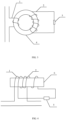
- the magnetic circuit core includes a closed magnetic circuit core 4, and the first coil 1 and the second coil 2 are both wound on the closed magnetic circuit core 4, for example, as shown in FIG. 2 .
- the winding methods of the first coil 1 and the second coil 2 mentioned above may be as follows: the first coil 1 is wound on the closed magnetic core 4, and the second coil 2 is wound on the first coil 1; or the second coil 2 is wound on the closed magnetic circuit core 4, and the first coil 1 is wound on the second coil 2; or the first coil 1 and the second coil 2 are co-wound on the closed magnetic circuit core 4.
- the embodiment of the present disclosure does not limit the winding method of the first coil 1 and the second coil 2.
- the first coil 1 and the second coil 2 may be wound respectively at different positions on the closed magnetic circuit core 4.
- the first coil 1 is connected to the operating circuit to enable the second coil 2 to generate the induced current.
- the current regulating device 5 is configured to regulate the magnitude of the current in the second coil 2, and then the magnitude of the magnetic flux of the closed magnetic circuit core 4 is changed. At this moment, the inductance of the inductor in the inductor assembly is regulated.
- the closed magnetic circuit core 4 may be in various structures.
- the closed magnetic circuit core may be a ring structure, or a double-C-shaped structure with notches butted against each other, or a ring structure with a slit on the side wall, or the like.
- the inductor assembly further includes an open magnetic circuit core 6.
- the first coil 1 is wound on the open magnetic circuit core 6, and the second coil 2 is wound on the first coil 1.
- the second coil 2 is wound on the open magnetic circuit core 6, and the first coil 1 is wound on the second coil 2.
- the first coil 1 and the second coil 2 are co-wound on the open magnetic circuit core 6.
- the first coil 1 is connected to the operating circuit to enable the second coil 2 to generate the induced current.
- the current regulating device 5 is configured to regulate the magnitude of the current in the second coil 2, and then the magnitude of the magnetic flux of the open magnetic circuit core 6 is changed. At this moment, the inductance of the inductor in the inductor assembly is regulated.
- the embodiment of the present disclosure does not limit the structure of the open magnetic circuit core 6.
- the open magnetic circuit core 6 may be a rod-shaped structure.
- the current regulating device 5 includes a variable resistor 3.
- the current regulating device includes a rectifier switching device.
- the variable resistor 3 and the rectifier switching device are described respectively:
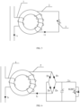
- the variable resistor 3 is a resistor whose resistance may be adjusted. As shown in FIG. 5 , the second coil 2 may be connected in series to the variable resistor 3 through wires (or another optional connection method), then the total resistance of the circuit where the second coil 2 is disposed is equal to the sum of the resistance of the second coil 2 and that of the variable resistor 3.
- the resistance value of the variable resistor 3 is adjusted, so as to change the total resistance of the circuit where the second coil 2 is disposed, thereby changing the current of the circuit where the second coil 2 is disposed.
- the magnetic flux of the second coil 2 is changed, and the inductance of the first coil 1 is changed accordingly. At this moment, the inductance of the inductor is regulated.
- the rectifier switching device is an insulated gate bipolar transistor.
- the insulated gate bipolar transistor (IGBT): it is a semiconductor element with a switching function.
- the application circuit of the IGBT is shown in FIG. 6 in which D1, D2, D3, D4, and D5 all represent diodes, C represents a capacitor, and L 1 represents an inductor.
- the IGBT and D5 are connected in parallel, and the IGBT and D5 in parallel are configured as a first element, then the first element and the inductor L 1 are connected in series to form a first sub-circuit.
- the first sub-circuit is connected in parallel to the capacitor C to form a branch circuit.
- two ends of the second coil 2 are connected in series to the branch circuit by D 2 and D 3 when the direction of the current I 2 in the second coil 2 is the direction shown in FIG. 6 . Accordingly, when the direction of the current I 2 in the second coil 2 is opposite to the direction shown in FIG. 6 , two ends of the second coil 2 are connected in series to the branch circuit through D 1 and D 4 . It can be seen that the second coil 2 is always connected in series to the branch circuit, that is, the circuit where the second coil 2 is disposed is always a closed circuit.
- the switching state of the IGBT may be changed by a computer.
- the value of the current in the circuit where the second coil 2 is disposed decreases; when the IGBT is switched from the off state to the on state, the value of the current in the second coil 2 is increased. Therefore, by regulating the switching frequencies of the IGBT by a computer, the switching states of the IGBT may be switched regularly, and the value of the current in the circuit where the second coil 2 is disposed will be changed accordingly, thus the effective value of I 2 is changed, and the current of the circuit where the second coil 2 is disposed may be adjusted. Therefore, the magnetic flux of the second coil 2 is changed, and the inductance of the first coil 1 is changed accordingly. At this moment, the inductance of the inductor is regulated.
- the function of the capacitor C is that when the switching state of the IGBT is changed, the capacitor may enable the current in the circuit where the second coil 2 is disposed to change, thereby preventing the current waveform of the circuit where the second coil 2 is disposed form being changed.
- the functions of the inductor L 1 are to prevent the generation of a surge current and protect the IGBT.
- a peak current which is a surge current
- the induced current generated by the second coil 2 is configured as a steady-state current, and the value of the surge current is greater than that of the steady-state current.
- L 1 is configured to prevent the generation of the surge current to protect the IGBT
- the rectifier switching device may include a thyristor or a triode.
- the thyristor is also a semiconductor element with a switching function.
- the principle of regulating the inductance of inductor by a thyristor is the same as that by an IGBT, which is not repeated herein.
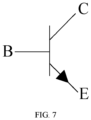
- the Triode the schematic diagram of the triode is shown in FIG. 7 in which B, C and E are the three electrodes of the triode respectively.
- the current from C to E is expressed as Ic
- the current from B to E is expressed as Ib
- the value of Ic changes as the value of Ib changes. Therefore, the two electrodes C and E may be connected to the two ends of the second coil 2 respectively, and then the current in the circuit where the second coil 2 is disposed is Ic.
- Ic is indirectly controlled by controlling Ib such that the magnetic flux of the second coil 2 is changed, and the inductance of the first coil 1 is also changed accordingly. At this moment, the inductance of the inductor is regulated.
- the embodiment of the present disclosure provides a speaker which includes a frequency divider.
- the frequency divider includes the above-mentioned inductor assembly.
- the speaker also has the above advantages of the inductor assembly.
- a user may regulate the inductance according to his or her own preference, such that the frequency divider may better divide the frequencies of the speaker and make the response frequencies of the speaker become wider.
- the structure of the speaker is common in the art, and it is also common in the art to provide a frequency divider and an inductor assembly in the speaker.
- a reference may be made to patents such as the application No. CN00240314 . 5 entitled HIGH-FIDELITY SPEAKER.
Landscapes
- Engineering & Computer Science (AREA)
- Power Engineering (AREA)
- Coils Or Transformers For Communication (AREA)
- Amplifiers (AREA)
Description
- The present disclosure relates to the field of electrical devices, and more particularly, relates to an inductor assembly and a speaker.
- An inductor is an element configured to convert electrical energy into magnetic energy and store the magnetic energy, which is an important part of the power system. In the power system, with a large number of non-linear loads being connected, problems such as voltage fluctuations and harmonic pollution may be caused. In order to solve these problems, the inductance of the inductor shall be adjusted during the operation.
- An inductor that uses a saturation inductance method to adjust the inductance is provided in related art. The inductor includes a core, a first coil and a second coil which are wound on the core. The first coil is configured to be connected to an operating circuit (the current in the operating circuit is an alternating current), which enables the second coil to generate an induced current. When the inductance of the inductor needs to be adjusted, it is necessary to apply direct current to the second coil, and constantly change a magnitude of the direct current, so as to change a saturation degree of the core, then change a magnitude of the inductance of the first coil, and adjust an inductance of the inductor.
- The inventors have found at least the following problems in the related art:
- In the related art, when the magnitude of the inductance of the inductor is changed, it is necessary to apply direct current to the second coil, and constantly change the magnitude of the direct current, and the operation is complex.
-
JP2004140165A -
CN1790565A describes a non-contact controllable reactor, which separates the dc control winding and ac operating winding in space, uses the adjustable hollow solenoid, the hollow solenoid with variable dc excitation, and the semi-iron core/circular-iron core straight solenoid with dc excitation as control winding. Wherein, regulating the reactance value by changing magnetic flux, controlling the magnetic saturation degree of semi-iron core, and controlling the rotation direction of magnetic domain of circular-iron core in cross magnetic field, improving the nonlinear character of traditional product, reducing harmonic wave quantity and reactor volume. -
RU2348998C1 -
CN202309082U describes an automatic stepless voltage regulating type reactive power compensator, which includes a capacitor set and a control portion thereof, wherein the line of the capacitor set connected to the electric network is serially connected with an adjustable reactor; the adjustable reactor comprises a primary side coil serially connected between the capacitor set and the electric network; the adjustable reactor is provided with a secondary control coil, with a bidirectional thyristor being connected between two ends of the secondary control coil; the control electrode of the bidirectional thyristor is connected with the intelligent controller; a detecting apparatus of the electric network reactive current is arranged upon the line of the capacitor set connected to the electric network; and the output of the detecting apparatus of the electric network reactive current is connected with the intelligent controller. - Embodiments of the present invention provide an inductor assembly and a speaker, which may solve the above-mentioned technical problems. The technical solutions are as follows:
- In one aspect, embodiments of the present invention provide an inductor assembly. The inductor assembly includes an inductor and a current regulating device;
- wherein the inductor includes a first coil and a second coil;
- wherein the second coil is configured to generate an induced current when an alternating current is flowing through; and
- two ends of the second coil are connected to the current regulating device in series by means of conducting wires, and the current regulating device comprises a first diode, a second diode, a third diode, a fourth diode, a capacitor, an inductor, a fifth diode and an insulated gate bipolar transistor, wherein
- one end of the second coil is connected to a cathode of the first diode and an anode of the third diode, another end of the second coil is connected to a cathode of the second diode and an anode of the fourth diode,
- an anode of the first diode is connected to an anode of the second diode, one plate of the capacitor, a source of the insulated gate bipolar transistor and an anode of the fifth diode, respectively,
- a cathode of the third diode is connected to a cathode of the fourth diode, another plate of the capacitor and one end of the inductor, respectively,
- another end of the inductor is connected to a drain of insulated gate bipolar transistor and a cathode of the fifth diode, respectively.
- Optionally, the first coil and the second coil are both air-core coils; and
- the second coil is wound on the first coil; or
- the first coil is wound on the second coil; or
- the first coil and the second coil are co-wound.
- Optionally, the inductor further includes a magnetic circuit core;
wherein the first coil and the second coil are both wound on the magnetic circuit core. - Optionally, the magnetic circuit core includes a closed magnetic circuit core; wherein
- the first coil is wound on the closed magnetic circuit core, and the second coil is wound on the first coil; or
- the second coil is wound on the closed magnetic circuit core, and the first coil is wound on the second coil; or
- the first coil and the second coil are co-wound on the closed magnetic circuit core.
- Optionally, the closed magnetic circuit core is one of a ring-shaped core and a ring-shaped core with a slit on a side wall.
- Optionally, the magnetic circuit core includes an open magnetic circuit core; wherein
- the first coil is wound on the open magnetic circuit core, and the second coil is wound on the first coil; or
- the second coil is wound on the open magnetic circuit core, and the first coil is wound on the second coil; or
- the first coil and the second coil are co-wound on the open magnetic circuit core.
- Optionally, the open magnetic circuit core is a rod-shaped core.
- In another aspect, embodiments of the present invention provide a speaker. The speaker includes a frequency divider;
wherein the frequency divider includes the above-mentioned inductor assembly. - In the inductor assembly according to the embodiments of the present invention, a first coil, a second coil, and a current regulating device are provided, and two ends of the second coil are connected to the current regulating device in series by means of conducting wires. After the first coil is connected to an operating circuit, the second coil is enabled to generate an induced current. When an inductance of the inductor in the inductor assembly needs to be changed, only the current regulating device needs to be regulated, and the operations are simple.
- In order to describe the technical solutions in the embodiments of the present disclosure more clearly, the following briefly introduces the accompanying drawings required for describing the embodiments. Apparently, the accompanying drawings in the following description show merely some embodiments of the present disclosure, and a person of ordinary skill in the art may also derive other drawings from these accompanying drawings without creative efforts.
-
FIG. 1 is a schematic structural circuit diagram of an inductor assembly according to an embodiment of the present disclosure; -
FIG. 2 is a schematic structural circuit diagram of an inductor assembly according to an embodiment of the present disclosure; -
FIG. 3 is a schematic structural circuit diagram of an inductor assembly according to an embodiment of the present disclosure; -
FIG. 4 is a schematic structural circuit diagram of an inductor assembly according to an embodiment of the present disclosure; -
FIG. 5 is a schematic structural circuit diagram of an inductor assembly according to an embodiment that does not form part of the present invention. -
FIG. 6 is a schematic structural circuit diagram of an inductor assembly according to an embodiment of the present disclosure; and -
FIG. 7 is a schematic structural diagram of a triode. - 1-first coil,
- 2-second coil,
- 3-variable resistor,
- 4-closed magnetic circuit core,
- 5-current regulating device, and
- 6-open magnetic circuit core.
- For clearer descriptions of the objects, technical solutions and advantages in the present disclosure, the present disclosure is described in detail below in combination with the accompanying drawings.
- An inductor is an element configured to convert electrical energy into magnetic energy and store the the magnetic energy, and is widely used in life. When the inductor is used, it is often necessary to adjust the inductance of the inductor.
- For the adjustment of the inductance of the inductor, a thyristor-controlled transformer (TCT) principle is adopted for adjustment in related art I. However, because the structure of the transformer is too complicated, it is of poor practicability. In related art II, the saturation inductance method is configured for adjustment. The inductor used in this method includes a core, a first coil and a second coil which are wound on the core. During the adjustment process, apply direct current to the second coil, and constantly change the magnitude of the direct current, so as to change the saturation degree of the core, and then change the magnitude of the inductance of the first coil. This method will cause current flowing through the inductor to be distorted or generate harmonics.
- In the embodiment of the present disclosure, the induced current generated by the second coil is configured to change a magnitude of a reverse magnetic flux by changing a magnitude of the current flowing through the second coil, so as to realize linear adjustment of the inductance of the inductor. The adjustment process is simple, and the air-core inductor, the open magnetic circuit inductor, and the closed-loop magnetic circuit inductor may all be linearly adjusted, which not only responds quickly, but also does not distort a waveform of the current flowing through the first coil.
- Taking the closed-loop magnetic circuit inductor as an example, the principle of the adjustment process is explained as follows: the closed-loop magnetic circuit inductor includes a first coil, a second coil and a closed magnetic circuit core. When I1N1=I2N2, in an ideal state, the magnetic flux of the closed magnetic circuit core is zero. In the formula, I1 is the current in the first coil, N1 is the number of turns of the first coil, I2 is the current in the second coil, and N2 is the number of turns of the second coil. At this moment, when the magnitude of the current in the second coil is changed, a magnetic flux generated by the second coil and the magnetic flux generated by the first coil cancel each other, and the magnetic flux of the closed magnetic circuit core is also changed, such that the inductance of the first coil is changed, thus the adjustment of the inductance of the inductor is achieved.
- In this regard, in one aspect, an embodiment of the present disclosure provides an inductor assembly. As shown in
FIG. 1 , the inductor includes an inductor and acurrent regulating device 5. The inductor includes afirst coil 1 and asecond coil 2, wherein thefirst coil 1 is configured to, after being connected to an operating circuit, enable thesecond coil 2 to generate an induced current; two ends of thesecond coil 2 are connected to thecurrent regulating device 5 in series by means of conducting wires, and thecurrent regulating device 5 is configured to regulate the magnitude of the induced current generated by thesecond coil 2. - The
first coil 1 is connected to the operating circuit (it may be understood that the current applied at this moment to thefirst coil 1 is an alternating current), which enables thesecond coil 2 to generate an induced current. When the inductance of the inductor in the inductor assembly needs to be changed, thecurrent regulating device 5 is configured to regulate a magnitude of current in thesecond coil 2, and then a magnitude of a magnetic flux of thesecond coil 2 is changed. At this moment, an inductance of the inductor in the inductor assembly is regulated. Here, the "operating circuit" refers to the circuit where a load is disposed. - In the inductor assembly according to the embodiment of the present disclosure, a
first coil 1, asecond coil 2, and acurrent regulating device 5 are provided, and two ends of thesecond coil 2 are connected to thecurrent regulating device 5 in series by means of conducting wires. After thefirst coil 1 is connected to an operating circuit, thesecond coil 2 is enabled to generate an induced current. When the inductance of the inductor in the inductor assembly needs to be changed, only thecurrent regulating device 5 needs to be regulated, and the operations are simple. - It should be noted that inductors with various structures are all applicable to the inductor assembly according to the embodiment of the present disclosure, and the following is optional:
- As an example, both the
first coil 1 and thesecond coil 2 may be arranged as air-core coils, and thesecond coil 2 is wound on thefirst coil 1. Alternatively, thefirst coil 1 is wound on thesecond coil 2. Alternatively, thefirst coil 1 and thesecond coil 2 are co-wound. - With this arrangement, the inductor assembly may be applied to occasions with a wide range of frequencies, ensuring that most audio frequencies may pass through smoothly.
- Here, the term "co-wound" refers to that the
first coil 1 and thesecond coil 2 are mixed and co-wound to form a layer of air-core coils (in each of the above-mentioned situation in which thesecond coil 2 is wound on thefirst coil 1, or thefirst coil 1 is wound on thesecond coil 2, thefirst coil 1 and thesecond coil 2 form two layers of air-core coils). In a possible implementation, two wires are placed side by side for winding. With reference toFIG. 1 , it may be seen that in the above-mentioned layer of air-core coils, the wires belonging to thefirst coil 1 are arranged alternately with the wires belonging to thesecond coil 2. - As another example, as shown in
FIG. 1 , the inductor assembly further includes a magnetic circuit core. Thefirst coil 1 and thesecond coil 2 are both wound on the magnetic circuit core. - In an optional embodiment, the magnetic circuit core includes a closed
magnetic circuit core 4, and thefirst coil 1 and thesecond coil 2 are both wound on the closedmagnetic circuit core 4, for example, as shown inFIG. 2 . Optionally, the winding methods of thefirst coil 1 and thesecond coil 2 mentioned above may be as follows: thefirst coil 1 is wound on the closedmagnetic core 4, and thesecond coil 2 is wound on thefirst coil 1; or thesecond coil 2 is wound on the closedmagnetic circuit core 4, and thefirst coil 1 is wound on thesecond coil 2; or thefirst coil 1 and thesecond coil 2 are co-wound on the closedmagnetic circuit core 4. The embodiment of the present disclosure does not limit the winding method of thefirst coil 1 and thesecond coil 2. For example, as shown inFIG. 3 , thefirst coil 1 and thesecond coil 2 may be wound respectively at different positions on the closedmagnetic circuit core 4. - In this embodiment, the
first coil 1 is connected to the operating circuit to enable thesecond coil 2 to generate the induced current. When it is necessary to change the inductance of the inductor in the inductor assembly, thecurrent regulating device 5 is configured to regulate the magnitude of the current in thesecond coil 2, and then the magnitude of the magnetic flux of the closedmagnetic circuit core 4 is changed. At this moment, the inductance of the inductor in the inductor assembly is regulated. By this arrangement, it is ensured that the magnetic resistance of the inductor is small and the magnetic induction intensity is large. - The closed
magnetic circuit core 4 may be in various structures. For example, the closed magnetic circuit core may be a ring structure, or a double-C-shaped structure with notches butted against each other, or a ring structure with a slit on the side wall, or the like. - As yet another example, the inductor assembly further includes an open
magnetic circuit core 6. Thefirst coil 1 is wound on the openmagnetic circuit core 6, and thesecond coil 2 is wound on thefirst coil 1. Alternatively, thesecond coil 2 is wound on the openmagnetic circuit core 6, and thefirst coil 1 is wound on thesecond coil 2. Alternatively, thefirst coil 1 and thesecond coil 2 are co-wound on the openmagnetic circuit core 6. For the schematic diagram of the winding methods, reference may be made toFIG. 4 . - The
first coil 1 is connected to the operating circuit to enable thesecond coil 2 to generate the induced current. When it is necessary to change the inductance of the inductor in the inductor assembly, thecurrent regulating device 5 is configured to regulate the magnitude of the current in thesecond coil 2, and then the magnitude of the magnetic flux of the openmagnetic circuit core 6 is changed. At this moment, the inductance of the inductor in the inductor assembly is regulated. By this arrangement, it is ensured that the magnetic resistance of the inductor is small and the magnetic induction intensity is large. - The embodiment of the present disclosure does not limit the structure of the open
magnetic circuit core 6. For example, the openmagnetic circuit core 6 may be a rod-shaped structure. - In an embodiment not covered by the present invention, the
current regulating device 5 includes avariable resistor 3. According to the present invention, the current regulating device includes a rectifier switching device. Next, thevariable resistor 3 and the rectifier switching device are described respectively: - The variable resistor 3: the
variable resistor 3 is a resistor whose resistance may be adjusted. As shown inFIG. 5 , thesecond coil 2 may be connected in series to thevariable resistor 3 through wires (or another optional connection method), then the total resistance of the circuit where thesecond coil 2 is disposed is equal to the sum of the resistance of thesecond coil 2 and that of thevariable resistor 3. When the inductance of the inductor needs to be adjusted, the resistance value of thevariable resistor 3 is adjusted, so as to change the total resistance of the circuit where thesecond coil 2 is disposed, thereby changing the current of the circuit where thesecond coil 2 is disposed. Afterwards, the magnetic flux of thesecond coil 2 is changed, and the inductance of thefirst coil 1 is changed accordingly. At this moment, the inductance of the inductor is regulated. - The rectifier switching device: According to the present invention, the rectifier switching device is an insulated gate bipolar transistor.
- The insulated gate bipolar transistor (IGBT): it is a semiconductor element with a switching function. The application circuit of the IGBT is shown in
FIG. 6 in which D1, D2, D3, D4, and D5 all represent diodes, C represents a capacitor, and L1 represents an inductor. InFIG. 6 , the IGBT and D5 are connected in parallel, and the IGBT and D5 in parallel are configured as a first element, then the first element and the inductor L1 are connected in series to form a first sub-circuit. The first sub-circuit is connected in parallel to the capacitor C to form a branch circuit. After thefirst coil 1 is connected to the operating circuit, two ends of thesecond coil 2 are connected in series to the branch circuit by D2 and D3 when the direction of the current I2 in thesecond coil 2 is the direction shown inFIG. 6 . Accordingly, when the direction of the current I2 in thesecond coil 2 is opposite to the direction shown inFIG. 6 , two ends of thesecond coil 2 are connected in series to the branch circuit through D1 and D4. It can be seen that thesecond coil 2 is always connected in series to the branch circuit, that is, the circuit where thesecond coil 2 is disposed is always a closed circuit. - Further, the switching state of the IGBT may be changed by a computer. When the IGBT is switched from the on state to the off state, the value of the current in the circuit where the
second coil 2 is disposed decreases; when the IGBT is switched from the off state to the on state, the value of the current in thesecond coil 2 is increased. Therefore, by regulating the switching frequencies of the IGBT by a computer, the switching states of the IGBT may be switched regularly, and the value of the current in the circuit where thesecond coil 2 is disposed will be changed accordingly, thus the effective value of I2 is changed, and the current of the circuit where thesecond coil 2 is disposed may be adjusted. Therefore, the magnetic flux of thesecond coil 2 is changed, and the inductance of thefirst coil 1 is changed accordingly. At this moment, the inductance of the inductor is regulated. - It should be noted that, as shown in
FIG. 6 , the function of the capacitor C is that when the switching state of the IGBT is changed, the capacitor may enable the current in the circuit where thesecond coil 2 is disposed to change, thereby preventing the current waveform of the circuit where thesecond coil 2 is disposed form being changed. The functions of the inductor L1 are to prevent the generation of a surge current and protect the IGBT. At the moment when thefirst coil 1 is connected to the operating circuit, a peak current, which is a surge current, is generated in thesecond coil 2. After thefirst coil 1 is connected to the operating circuit, the induced current generated by thesecond coil 2 is configured as a steady-state current, and the value of the surge current is greater than that of the steady-state current. Thus, damages may be caused to the IGBT. Therefore, in the invention, L1 is configured to prevent the generation of the surge current to protect the IGBT - In examples that do not form part of the present invention, the rectifier switching device may include a thyristor or a triode. The thyristor is also a semiconductor element with a switching function. Moreover, the principle of regulating the inductance of inductor by a thyristor is the same as that by an IGBT, which is not repeated herein.
- The Triode: the schematic diagram of the triode is shown in
FIG. 7 in which B, C and E are the three electrodes of the triode respectively. The current from C to E is expressed as Ic, the current from B to E is expressed as Ib, and the value of Ic changes as the value of Ib changes. Therefore, the two electrodes C and E may be connected to the two ends of thesecond coil 2 respectively, and then the current in the circuit where thesecond coil 2 is disposed is Ic. After that, Ic is indirectly controlled by controlling Ib such that the magnetic flux of thesecond coil 2 is changed, and the inductance of thefirst coil 1 is also changed accordingly. At this moment, the inductance of the inductor is regulated. - In another aspect, the embodiment of the present disclosure provides a speaker which includes a frequency divider. The frequency divider includes the above-mentioned inductor assembly.
- It can be understood by those skilled in the art that the speaker also has the above advantages of the inductor assembly. By using the inductor assembly provided in the present disclosure, a user may regulate the inductance according to his or her own preference, such that the frequency divider may better divide the frequencies of the speaker and make the response frequencies of the speaker become wider.
- The structure of the speaker is common in the art, and it is also common in the art to provide a frequency divider and an inductor assembly in the speaker. For example, a reference may be made to patents such as the application No.
CN00240314 . 5 entitled HIGH-FIDELITY SPEAKER. - Described above are merely embodiments of the present disclosure, and are not intended to limit the protection scope of the present disclosure which is only limited by the appended claims.
Claims (8)
- An inductor assembly, wherein the inductor assembly comprises: an inductor and a current regulating device (5); whereinthe inductor comprises: a first coil (1) and a second coil (2); whereinthe second coil (2) is configured to generate an induced current when an alternating current is flowing through the first coil (1); andtwo ends of the second coil (2) are connected in series to the current regulating device (5) by a conducting wire, and the current regulating device (5) comprises an insulated gate bipolar transistor;characterized in that the current regulating device (5) further comprisesa first diode, D1, a second diode, D2, a third diode, D3, a fourth diode, D4, a capacitor, C, an inductor, L1, and a fifth diode, D5, wherein:one end of the second coil (2) is connected to a cathode of the first diode, D1, and an anode of the third diode, D3, another end of the second coil (2) is connected to a cathode of the second diode, D2, and an anode of the fourth diode, D4,an anode of the first diode, D1, is connected to an anode of the second diode, D2, one plate of the capacitor, C, a source of the insulated gate bipolar transistor, IGBT, and an anode of the fifth diode, D5, respectively,a cathode of the third diode, D3, is connected to a cathode of the fourth diode, D4, another plate of the capacitor, C, and one end of the inductor, L1, respectively,another end of the inductor, L1, is connected to a drain of insulated gate bipolar transistor, IGBT, and a cathode of the fifth diode, D5, respectively.
- The inductor assembly according to claim 1, whereinthe first coil (1) and the second coil (2) are both air-core coils; andthe second coil (2) is wound on the first coil (1); orthe first coil (1) is wound on the second coil (2); orthe first coil (1) and the second coil (2) are co-wound.
- The inductor assembly according to claim 1, wherein the inductor assembly further comprises a magnetic circuit core;
wherein the first coil (1) and the second coil (2) are both wound on the magnetic circuit core. - The inductor assembly according to claim 3, wherein the magnetic circuit core comprises a closed magnetic circuit core (4); whereinthe first coil (1) is wound on the closed magnetic circuit core (4), and the second coil (2) is wound on the first coil (1); orthe second coil (2) is wound on the closed magnetic circuit core (4), and the first coil (1) is wound on the second coil (2); oralternatively, the first coil (1) and the second coil (2) are co-wound on the closed magnetic circuit core (4).
- The inductor assembly according to claim 4, wherein the closed magnetic circuit core (4) is one of a ring-shaped core and a ring-shaped core with a slit on a side wall.
- The inductor assembly according to claim 3, wherein the magnetic circuit core comprises: an open magnetic circuit core (6); whereinthe first coil (1) is wound on the open magnetic circuit core (6), and the second coil (2) is wound on the first coil (1); orthe second coil (2) is wound on the open magnetic circuit core (6), and the first coil (1) is wound on the second coil (2); orthe first coil (1) and the second coil (2) are co-wound on the open magnetic circuit core (6).
- The inductor assembly according to claim 6, wherein the open magnetic circuit core (6) is a rod-shaped core.
- A speaker, comprising a frequency divider, wherein the frequency divider comprises the inductor assembly as defined in any one of claims 1 to 7.
Applications Claiming Priority (2)
| Application Number | Priority Date | Filing Date | Title |
|---|---|---|---|
| CN201810067576.8A CN108447665A (en) | 2018-01-24 | 2018-01-24 | A kind of controllable impedance device assembly and speaker |
| PCT/CN2019/072866 WO2019144887A1 (en) | 2018-01-24 | 2019-01-23 | Inductor assembly and speaker |
Publications (4)
| Publication Number | Publication Date |
|---|---|
| EP3736840A1 EP3736840A1 (en) | 2020-11-11 |
| EP3736840A4 EP3736840A4 (en) | 2021-03-10 |
| EP3736840C0 EP3736840C0 (en) | 2023-08-23 |
| EP3736840B1 true EP3736840B1 (en) | 2023-08-23 |
Family
ID=63191298
Family Applications (1)
| Application Number | Title | Priority Date | Filing Date |
|---|---|---|---|
| EP19743230.5A Active EP3736840B1 (en) | 2018-01-24 | 2019-01-23 | Inductor assembly and speaker |
Country Status (3)
| Country | Link |
|---|---|
| EP (1) | EP3736840B1 (en) |
| CN (2) | CN108447665A (en) |
| WO (1) | WO2019144887A1 (en) |
Families Citing this family (5)
| Publication number | Priority date | Publication date | Assignee | Title |
|---|---|---|---|---|
| CN108447665A (en) * | 2018-01-24 | 2018-08-24 | 北京金科华业测控技术有限公司 | A kind of controllable impedance device assembly and speaker |
| CN110379611A (en) * | 2019-06-26 | 2019-10-25 | 东南大学 | A kind of DC current control inductance tuner with permanent magnet bias |
| CN112350204A (en) * | 2019-11-20 | 2021-02-09 | 邹虚 | Movable transformer substation |
| CN118098791A (en) * | 2022-11-28 | 2024-05-28 | 王静然 | Inductors and speaker components |
| CN119786227B (en) * | 2025-03-07 | 2025-05-09 | 深圳市海瑞思自动化科技有限公司 | Radio frequency coil inductance value adjusting device for mass spectrum |
Family Cites Families (16)
| Publication number | Priority date | Publication date | Assignee | Title |
|---|---|---|---|---|
| US4207530A (en) * | 1977-09-12 | 1980-06-10 | Motorola, Inc. | Electrically tunable inductor and method |
| JPH05182837A (en) * | 1992-01-07 | 1993-07-23 | Matsushita Electric Ind Co Ltd | Variable inductor |
| US20040012472A1 (en) * | 1997-11-28 | 2004-01-22 | Christian Sasse | Flux control for high power static electromagnetic devices |
| CN2455028Y (en) * | 2000-11-29 | 2001-10-17 | 梁耀辉 | High-fidelity voice |
| JP2004140165A (en) * | 2002-10-17 | 2004-05-13 | Matsushita Electric Ind Co Ltd | Variable inductor |
| CN100483575C (en) * | 2005-12-23 | 2009-04-29 | 清华大学 | Non-contact controllable reactor |
| RU2348998C1 (en) * | 2008-01-31 | 2009-03-10 | Александр Васильевич Григорьев | Controllable transformer-type reactor |
| CN201319287Y (en) * | 2008-12-03 | 2009-09-30 | 上海铁路通信工厂 | Heavy-current hollow coil |
| US20110260819A1 (en) * | 2010-04-26 | 2011-10-27 | Taiwan Semiconductor Manufacturing Co., Ltd. | Continuously tunable inductor with variable resistors |
| CN202309082U (en) * | 2011-09-28 | 2012-07-04 | 武汉伏特克电气工程有限公司 | Automatic stepless voltage regulating type reactive power compensator |
| CN102682955B (en) * | 2012-05-10 | 2016-09-14 | 杭州金果科技有限公司 | A kind of controllable impedance |
| CN202759249U (en) * | 2012-08-23 | 2013-02-27 | 大连第二互感器集团有限公司 | Magnetic control parallel reactor |
| CN203311972U (en) * | 2013-07-11 | 2013-11-27 | 哈尔滨理工大学 | An adjustable reactor with air gap DC magnetic control |
| CN204992589U (en) * | 2015-10-10 | 2016-01-20 | 张家港市博特圣电气科技有限公司 | Three -phase AC intelligent control circuit |
| CN107509134A (en) * | 2017-10-10 | 2017-12-22 | 李龙根 | A kind of earphone second order passive frequency divider |
| CN108447665A (en) * | 2018-01-24 | 2018-08-24 | 北京金科华业测控技术有限公司 | A kind of controllable impedance device assembly and speaker |
-
2018
- 2018-01-24 CN CN201810067576.8A patent/CN108447665A/en active Pending
-
2019
- 2019-01-23 WO PCT/CN2019/072866 patent/WO2019144887A1/en not_active Ceased
- 2019-01-23 EP EP19743230.5A patent/EP3736840B1/en active Active
- 2019-01-23 CN CN201980021874.6A patent/CN111954913A/en active Pending
Also Published As
| Publication number | Publication date |
|---|---|
| EP3736840C0 (en) | 2023-08-23 |
| EP3736840A4 (en) | 2021-03-10 |
| CN111954913A (en) | 2020-11-17 |
| CN108447665A (en) | 2018-08-24 |
| EP3736840A1 (en) | 2020-11-11 |
| WO2019144887A1 (en) | 2019-08-01 |
Similar Documents
| Publication | Publication Date | Title |
|---|---|---|
| EP3736840A1 (en) | Inductor assembly and speaker | |
| US10992217B2 (en) | Insulated power source and power conversion device | |
| US5942884A (en) | Electronic transformer/regulator | |
| EP2340609A2 (en) | Voltage control and power factor correction in ac induction motors | |
| US8169756B2 (en) | Fault current limiting | |
| DE19702042A1 (en) | Voltage supply for high power load from mains of arbitrary voltage | |
| EP3841602B1 (en) | Current control apparatus | |
| CN110914934B (en) | Resonant converter with variable inductor | |
| KR101925182B1 (en) | Inductive Power Supply based on Current Transformer | |
| US20200153354A1 (en) | Controlling voltage in ac power lines | |
| CN119446716A (en) | A flexible distribution transformer and installation equipment for AC and DC distribution network | |
| CN115811238A (en) | AC electronic transformer or voltage regulator | |
| KR101617857B1 (en) | Power saving of device | |
| CN201364801Y (en) | Flux cancellation reactor | |
| US5319534A (en) | Series-parallel active power line conditioner utilizing reduced-turns-ratio transformer for enhanced peak voltage regulation capability | |
| US20120314728A1 (en) | System and method to deliver and control power to an arc furnace | |
| US20100067274A1 (en) | Method and device for creating a direct voltage or a direct current | |
| JP2020141555A (en) | Automatic device for compensating for reactive component loss in ac network and method thereof | |
| US9343996B2 (en) | Method and system for transmitting voltage and current between a source and a load | |
| US4896091A (en) | Electric power converter | |
| CN104485824A (en) | Multifunctional transformer with isolated magnetic control | |
| CN102158104A (en) | Voltage and current regulator | |
| RU2065654C1 (en) | Variable reactor | |
| JP3582721B2 (en) | DC-DC converter | |
| RU2554712C1 (en) | Stabilising ac voltage regulator |
Legal Events
| Date | Code | Title | Description |
|---|---|---|---|
| STAA | Information on the status of an ep patent application or granted ep patent |
Free format text: STATUS: THE INTERNATIONAL PUBLICATION HAS BEEN MADE |
|
| PUAI | Public reference made under article 153(3) epc to a published international application that has entered the european phase |
Free format text: ORIGINAL CODE: 0009012 |
|
| STAA | Information on the status of an ep patent application or granted ep patent |
Free format text: STATUS: REQUEST FOR EXAMINATION WAS MADE |
|
| 17P | Request for examination filed |
Effective date: 20200804 |
|
| AK | Designated contracting states |
Kind code of ref document: A1 Designated state(s): AL AT BE BG CH CY CZ DE DK EE ES FI FR GB GR HR HU IE IS IT LI LT LU LV MC MK MT NL NO PL PT RO RS SE SI SK SM TR |
|
| AX | Request for extension of the european patent |
Extension state: BA ME |
|
| A4 | Supplementary search report drawn up and despatched |
Effective date: 20210209 |
|
| RIC1 | Information provided on ipc code assigned before grant |
Ipc: H01F 27/42 20060101ALI20210203BHEP Ipc: H01F 27/28 20060101ALI20210203BHEP Ipc: H01F 21/02 20060101ALI20210203BHEP Ipc: H01F 27/40 20060101AFI20210203BHEP Ipc: H01F 21/12 20060101ALI20210203BHEP |
|
| DAV | Request for validation of the european patent (deleted) | ||
| DAX | Request for extension of the european patent (deleted) | ||
| RIC1 | Information provided on ipc code assigned before grant |
Ipc: H01F 21/02 20060101ALI20230119BHEP Ipc: H01F 27/42 20060101ALI20230119BHEP Ipc: H01F 21/12 20060101ALI20230119BHEP Ipc: H01F 27/28 20060101ALI20230119BHEP Ipc: H01F 27/40 20060101AFI20230119BHEP |
|
| GRAP | Despatch of communication of intention to grant a patent |
Free format text: ORIGINAL CODE: EPIDOSNIGR1 |
|
| STAA | Information on the status of an ep patent application or granted ep patent |
Free format text: STATUS: GRANT OF PATENT IS INTENDED |
|
| INTG | Intention to grant announced |
Effective date: 20230307 |
|
| GRAS | Grant fee paid |
Free format text: ORIGINAL CODE: EPIDOSNIGR3 |
|
| GRAA | (expected) grant |
Free format text: ORIGINAL CODE: 0009210 |
|
| STAA | Information on the status of an ep patent application or granted ep patent |
Free format text: STATUS: THE PATENT HAS BEEN GRANTED |
|
| AK | Designated contracting states |
Kind code of ref document: B1 Designated state(s): AL AT BE BG CH CY CZ DE DK EE ES FI FR GB GR HR HU IE IS IT LI LT LU LV MC MK MT NL NO PL PT RO RS SE SI SK SM TR |
|
| REG | Reference to a national code |
Ref country code: GB Ref legal event code: FG4D |
|
| REG | Reference to a national code |
Ref country code: CH Ref legal event code: EP |
|
| REG | Reference to a national code |
Ref country code: DE Ref legal event code: R096 Ref document number: 602019035615 Country of ref document: DE |
|
| REG | Reference to a national code |
Ref country code: IE Ref legal event code: FG4D |
|
| U01 | Request for unitary effect filed |
Effective date: 20230823 |
|
| U07 | Unitary effect registered |
Designated state(s): AT BE BG DE DK EE FI FR IT LT LU LV MT NL PT SE SI Effective date: 20230901 |
|
| U1N | Appointed representative for the unitary patent procedure changed after the registration of the unitary effect |
Representative=s name: CHUNG, HOI KAN; GB |
|
| U20 | Renewal fee for the european patent with unitary effect paid |
Year of fee payment: 6 Effective date: 20231205 |
|
| PG25 | Lapsed in a contracting state [announced via postgrant information from national office to epo] |
Ref country code: GR Free format text: LAPSE BECAUSE OF FAILURE TO SUBMIT A TRANSLATION OF THE DESCRIPTION OR TO PAY THE FEE WITHIN THE PRESCRIBED TIME-LIMIT Effective date: 20231124 |
|
| PGFP | Annual fee paid to national office [announced via postgrant information from national office to epo] |
Ref country code: GB Payment date: 20231122 Year of fee payment: 6 |
|
| PG25 | Lapsed in a contracting state [announced via postgrant information from national office to epo] |
Ref country code: IS Free format text: LAPSE BECAUSE OF FAILURE TO SUBMIT A TRANSLATION OF THE DESCRIPTION OR TO PAY THE FEE WITHIN THE PRESCRIBED TIME-LIMIT Effective date: 20231223 |
|
| PG25 | Lapsed in a contracting state [announced via postgrant information from national office to epo] |
Ref country code: RS Free format text: LAPSE BECAUSE OF FAILURE TO SUBMIT A TRANSLATION OF THE DESCRIPTION OR TO PAY THE FEE WITHIN THE PRESCRIBED TIME-LIMIT Effective date: 20230823 Ref country code: NO Free format text: LAPSE BECAUSE OF FAILURE TO SUBMIT A TRANSLATION OF THE DESCRIPTION OR TO PAY THE FEE WITHIN THE PRESCRIBED TIME-LIMIT Effective date: 20231123 Ref country code: IS Free format text: LAPSE BECAUSE OF FAILURE TO SUBMIT A TRANSLATION OF THE DESCRIPTION OR TO PAY THE FEE WITHIN THE PRESCRIBED TIME-LIMIT Effective date: 20231223 Ref country code: HR Free format text: LAPSE BECAUSE OF FAILURE TO SUBMIT A TRANSLATION OF THE DESCRIPTION OR TO PAY THE FEE WITHIN THE PRESCRIBED TIME-LIMIT Effective date: 20230823 Ref country code: GR Free format text: LAPSE BECAUSE OF FAILURE TO SUBMIT A TRANSLATION OF THE DESCRIPTION OR TO PAY THE FEE WITHIN THE PRESCRIBED TIME-LIMIT Effective date: 20231124 |
|
| PG25 | Lapsed in a contracting state [announced via postgrant information from national office to epo] |
Ref country code: PL Free format text: LAPSE BECAUSE OF FAILURE TO SUBMIT A TRANSLATION OF THE DESCRIPTION OR TO PAY THE FEE WITHIN THE PRESCRIBED TIME-LIMIT Effective date: 20230823 |
|
| PG25 | Lapsed in a contracting state [announced via postgrant information from national office to epo] |
Ref country code: ES Free format text: LAPSE BECAUSE OF FAILURE TO SUBMIT A TRANSLATION OF THE DESCRIPTION OR TO PAY THE FEE WITHIN THE PRESCRIBED TIME-LIMIT Effective date: 20230823 |
|
| PG25 | Lapsed in a contracting state [announced via postgrant information from national office to epo] |
Ref country code: SM Free format text: LAPSE BECAUSE OF FAILURE TO SUBMIT A TRANSLATION OF THE DESCRIPTION OR TO PAY THE FEE WITHIN THE PRESCRIBED TIME-LIMIT Effective date: 20230823 Ref country code: RO Free format text: LAPSE BECAUSE OF FAILURE TO SUBMIT A TRANSLATION OF THE DESCRIPTION OR TO PAY THE FEE WITHIN THE PRESCRIBED TIME-LIMIT Effective date: 20230823 Ref country code: ES Free format text: LAPSE BECAUSE OF FAILURE TO SUBMIT A TRANSLATION OF THE DESCRIPTION OR TO PAY THE FEE WITHIN THE PRESCRIBED TIME-LIMIT Effective date: 20230823 Ref country code: CZ Free format text: LAPSE BECAUSE OF FAILURE TO SUBMIT A TRANSLATION OF THE DESCRIPTION OR TO PAY THE FEE WITHIN THE PRESCRIBED TIME-LIMIT Effective date: 20230823 Ref country code: SK Free format text: LAPSE BECAUSE OF FAILURE TO SUBMIT A TRANSLATION OF THE DESCRIPTION OR TO PAY THE FEE WITHIN THE PRESCRIBED TIME-LIMIT Effective date: 20230823 |
|
| REG | Reference to a national code |
Ref country code: DE Ref legal event code: R097 Ref document number: 602019035615 Country of ref document: DE |
|
| PLBE | No opposition filed within time limit |
Free format text: ORIGINAL CODE: 0009261 |
|
| STAA | Information on the status of an ep patent application or granted ep patent |
Free format text: STATUS: NO OPPOSITION FILED WITHIN TIME LIMIT |
|
| 26N | No opposition filed |
Effective date: 20240524 |
|
| PG25 | Lapsed in a contracting state [announced via postgrant information from national office to epo] |
Ref country code: MC Free format text: LAPSE BECAUSE OF FAILURE TO SUBMIT A TRANSLATION OF THE DESCRIPTION OR TO PAY THE FEE WITHIN THE PRESCRIBED TIME-LIMIT Effective date: 20230823 |
|
| PG25 | Lapsed in a contracting state [announced via postgrant information from national office to epo] |
Ref country code: MC Free format text: LAPSE BECAUSE OF FAILURE TO SUBMIT A TRANSLATION OF THE DESCRIPTION OR TO PAY THE FEE WITHIN THE PRESCRIBED TIME-LIMIT Effective date: 20230823 |
|
| REG | Reference to a national code |
Ref country code: CH Ref legal event code: PL |
|
| PG25 | Lapsed in a contracting state [announced via postgrant information from national office to epo] |
Ref country code: CH Free format text: LAPSE BECAUSE OF NON-PAYMENT OF DUE FEES Effective date: 20240131 |
|
| PG25 | Lapsed in a contracting state [announced via postgrant information from national office to epo] |
Ref country code: CH Free format text: LAPSE BECAUSE OF NON-PAYMENT OF DUE FEES Effective date: 20240131 |
|
| PG25 | Lapsed in a contracting state [announced via postgrant information from national office to epo] |
Ref country code: IE Free format text: LAPSE BECAUSE OF NON-PAYMENT OF DUE FEES Effective date: 20240123 |
|
| PG25 | Lapsed in a contracting state [announced via postgrant information from national office to epo] |
Ref country code: IE Free format text: LAPSE BECAUSE OF NON-PAYMENT OF DUE FEES Effective date: 20240123 |
|
| PG25 | Lapsed in a contracting state [announced via postgrant information from national office to epo] |
Ref country code: CY Free format text: LAPSE BECAUSE OF FAILURE TO SUBMIT A TRANSLATION OF THE DESCRIPTION OR TO PAY THE FEE WITHIN THE PRESCRIBED TIME-LIMIT; INVALID AB INITIO Effective date: 20190123 |
|
| PG25 | Lapsed in a contracting state [announced via postgrant information from national office to epo] |
Ref country code: HU Free format text: LAPSE BECAUSE OF FAILURE TO SUBMIT A TRANSLATION OF THE DESCRIPTION OR TO PAY THE FEE WITHIN THE PRESCRIBED TIME-LIMIT; INVALID AB INITIO Effective date: 20190123 |
|
| U90 | Renewal fees not paid: noting of loss of rights |
Free format text: RENEWAL FEE NOT PAID FOR YEAR 07 Effective date: 20250819 |
|
| GBPC | Gb: european patent ceased through non-payment of renewal fee |
Effective date: 20250123 |
|
| PG25 | Lapsed in a contracting state [announced via postgrant information from national office to epo] |
Ref country code: GB Free format text: LAPSE BECAUSE OF NON-PAYMENT OF DUE FEES Effective date: 20250123 |
|
| U93 | Unitary patent lapsed |
Free format text: RENEWAL FEE NOT PAID Effective date: 20250131 |
|
| PG25 | Lapsed in a contracting state [announced via postgrant information from national office to epo] |
Ref country code: TR Free format text: LAPSE BECAUSE OF FAILURE TO SUBMIT A TRANSLATION OF THE DESCRIPTION OR TO PAY THE FEE WITHIN THE PRESCRIBED TIME-LIMIT Effective date: 20230823 |