EP3736657B1 - Processing system, related integrated circuit, device and method - Google Patents
Processing system, related integrated circuit, device and method Download PDFInfo
- Publication number
- EP3736657B1 EP3736657B1 EP20171289.0A EP20171289A EP3736657B1 EP 3736657 B1 EP3736657 B1 EP 3736657B1 EP 20171289 A EP20171289 A EP 20171289A EP 3736657 B1 EP3736657 B1 EP 3736657B1
- Authority
- EP
- European Patent Office
- Prior art keywords
- signal
- time
- circuit
- digital
- processing unit
- Prior art date
- Legal status (The legal status is an assumption and is not a legal conclusion. Google has not performed a legal analysis and makes no representation as to the accuracy of the status listed.)
- Active
Links
Images




Classifications
-
- G—PHYSICS
- G05—CONTROLLING; REGULATING
- G05B—CONTROL OR REGULATING SYSTEMS IN GENERAL; FUNCTIONAL ELEMENTS OF SUCH SYSTEMS; MONITORING OR TESTING ARRANGEMENTS FOR SUCH SYSTEMS OR ELEMENTS
- G05B19/00—Program-control systems
- G05B19/02—Program-control systems electric
- G05B19/04—Program control other than numerical control, i.e. in sequence controllers or logic controllers
- G05B19/042—Program control other than numerical control, i.e. in sequence controllers or logic controllers using digital processors
- G05B19/0423—Input/output
-
- G—PHYSICS
- G06—COMPUTING OR CALCULATING; COUNTING
- G06F—ELECTRIC DIGITAL DATA PROCESSING
- G06F1/00—Details not covered by groups G06F3/00 - G06F13/00 and G06F21/00
- G06F1/04—Generating or distributing clock signals or signals derived directly therefrom
-
- G—PHYSICS
- G06—COMPUTING OR CALCULATING; COUNTING
- G06F—ELECTRIC DIGITAL DATA PROCESSING
- G06F1/00—Details not covered by groups G06F3/00 - G06F13/00 and G06F21/00
- G06F1/04—Generating or distributing clock signals or signals derived directly therefrom
- G06F1/14—Time supervision arrangements, e.g. real time clock
-
- H—ELECTRICITY
- H03—ELECTRONIC CIRCUITRY
- H03K—PULSE TECHNIQUE
- H03K19/00—Logic circuits, i.e. having at least two inputs acting on one output; Inverting circuits
- H03K19/01—Modifications for accelerating switching
-
- H—ELECTRICITY
- H04—ELECTRIC COMMUNICATION TECHNIQUE
- H04L—TRANSMISSION OF DIGITAL INFORMATION, e.g. TELEGRAPHIC COMMUNICATION
- H04L12/00—Data switching networks
- H04L12/28—Data switching networks characterised by path configuration, e.g. LAN [Local Area Networks] or WAN [Wide Area Networks]
- H04L12/40—Bus networks
- H04L12/40169—Flexible bus arrangements
- H04L12/40176—Flexible bus arrangements involving redundancy
- H04L12/40182—Flexible bus arrangements involving redundancy by using a plurality of communication lines
-
- G—PHYSICS
- G05—CONTROLLING; REGULATING
- G05B—CONTROL OR REGULATING SYSTEMS IN GENERAL; FUNCTIONAL ELEMENTS OF SUCH SYSTEMS; MONITORING OR TESTING ARRANGEMENTS FOR SUCH SYSTEMS OR ELEMENTS
- G05B2219/00—Program-control systems
- G05B2219/20—Pc systems
- G05B2219/25—Pc structure of the system
- G05B2219/25257—Microcontroller
Definitions
- Embodiments of the present disclosure relate to the time management within processing systems, such as micro-controllers.
- FIG. 1 shows a typical electronic system, such as the electronic system of a vehicle, comprising a plurality of processing systems 10, such as embedded systems or integrated circuits, e.g ., a Field Programmable Gate Array (FPGA), a Digital Signal Processor (DSP) or a micro-controller (e.g., dedicated to the automotive market).
- processing systems 10 such as embedded systems or integrated circuits, e.g ., a Field Programmable Gate Array (FPGA), a Digital Signal Processor (DSP) or a micro-controller (e.g., dedicated to the automotive market).
- FPGA Field Programmable Gate Array
- DSP Digital Signal Processor
- micro-controller e.g., dedicated to the automotive market.
- the communication system may include a vehicle control bus, such as a Controller Area Network (CAN) bus, and possibly a multimedia bus, such as a Media Oriented Systems Transport (MOST) bus, connected to vehicle control bus via a gateway.
- vehicle control bus such as a Controller Area Network (CAN) bus
- multimedia bus such as a Media Oriented Systems Transport (MOST) bus
- the processing systems 10 are located at different positions of the vehicle and may include, e.g., an Engine Control Unit (ECU), a Transmission Control Unit (TCU), an Anti-lock Braking System (ABS), a body control modules (BCM), and/or a navigation and/or multimedia audio system.
- ECU Engine Control Unit
- TCU Transmission Control Unit
- ABS Anti-lock Braking System
- BCM body control modules
- Future generations of processing systems in particular micro-controllers dedicated to automotive applications, will exhibit a significant increase in complexity, mainly due to the increasing number of functionalities (such as new protocols, new features, etc.) and to the tight constraints concerning the operation conditions of the system (such as lower power consumption, increased calculation power and speed, etc.).
- FIG 2 shows a block diagram of an exemplary digital processing system 10, such as a micro-controller, which may be used as any of the processing systems 10 of Figure 1 .
- the processing system 10 comprises at least one processing unit 102, such as a microprocessor, usually the Central Processing Unit (CPU), programmed via software instructions.
- a processing unit 102 such as a microprocessor, usually the Central Processing Unit (CPU), programmed via software instructions.
- the software executed by the processing unit 102 is stored in a program memory 104, such as a non-volatile memory, such as a Flash memory or EEPROM.
- the memory 104 may be integrated with the processing unit 102 in a single integrated circuit, or the memory 104 may be in the form of a separate integrated circuit and connected to the processing unit 102, e.g. via the traces of a printed circuit board.
- the memory 104 contains the firmware for the processing unit 102, wherein the term firmware includes both the software of a micro-processor and the programming data of a programmable logic circuit, such as a FPGA.
- the processing unit 102 may have associated one or more resources 106 selected from the group of:
- the digital processing system 10 may support different functionalities.
- the behavior of the processing unit 102 is determined by the firmware stored in the memory 104a, e.g ., the software instructions to be executed by a microprocessor 102 of a micro-controller 10.
- the firmware stored in the memory 104a
- the processing systems 10 may control different operations of the vehicle, wherein the processing systems 10 may be located at different positions in the vehicle and each processing system 10 may implement one or more functions/operations. Many of these functions/operations have to be execute in real-time.
- the engine control is subject to thermodynamic laws that should be balanced with the real-time state of the vehicle.
- the real time state of the vehicle is monitored via sensors, which may be connected directly to the processing system 10 implementing the Engine Control Unit (ECU) or to other processing systems 10 of the vehicle.
- the Engine Control Unit (ECU) has to control/command one or more actuators, e . g . in order to inject the fuel, open a valve for gas discharge etc., which may be connected directly to the processing system 10 implementing the Engine Control Unit (ECU) or to other processing systems 10 of the vehicle.
- the execution of a first operation within a processing system 10 has to be synchronized with the execution of a second operation within the same processing system 10 or within a further processing system 10.
- the present invention relates to a processing system comprising a time reference circuit according to the preamble of Claim 1, which is known, e.g., from Hauke Webermann, "CAN Send and Receive With Hardware Timestamping", 8 March 2017 (2017-03-08), pages 04-06 .
- one or more of the above objectives is achieved by means of a processing system having the features specifically set forth in the claims that follow.
- Embodiments moreover concern a related integrated circuit, device and method.
- the processing system such as an integrated circuit, comprises a digital processing unit programmable as a function of a firmware stored to a non-volatile memory and a resource connected to the digital processing unit via a communication system.
- the processing system may be a microcontroller and the digital processing unit may be a microprocessor of the microcontroller.
- the processing system comprises moreover a time reference circuit comprising a first digital counter circuit configured to generate, in response to a clock signal, a system time signal comprising a plurality of bits indicative of a time tick-count.
- the first digital counter circuit of the time reference circuit is configured to generate the system time signal by increasing the value of the system time signal by a given amount in response to the clock signal. In various embodiments, this given amount may be programmable by means of the processing unit.
- the processing system comprises moreover a time base distribution circuit configured to generate a time base signal by selecting a subset of the bits of the system time signal.
- the time base distribution circuit is configured to generate a time base signal by selecting a first subset of a given number of bits of the system time signal when a selection signal has a first value, and a second subset of the given number of bits of the system time signal when the selection signal has a second value, whereby the time resolution of the time base signal varies as a function of the selection signal.
- the time base signal is provided to the resource.
- the resource may be configured to detect a given event, store the time base signal to a register in response to the event, and signal the event to the digital processing unit.
- the digital processing unit may, in response to the event having been signaled by the resource, read via the communication system the time base signal from the register.
- the resource may be an analog-to-digital converter and the event may correspond to the completion of an analog-to-digital conversion
- the resource may be a communication interface and the event may correspond to the reception of data via the communication interface.
- the time reference circuit may also comprise further circuits.
- the time reference circuit comprises an extended timer circuit comprising a second digital counter circuit configured to generate, in response to the clock signal or a trigger signal generated as a function of the clock signal, an extended system time signal comprising a number of bits being greater than the number of bits of the system time signal, wherein the extended system time signal is readable by means of the digital processing unit.
- the time reference circuit comprises an operation time counter circuit comprising a plurality of third digital counter circuits configured to generate, in response to the clock signal or a trigger signal generated as a function of the clock signal, respective count values, wherein each of the plurality of third digital counter circuits may be reset, started and stopped by the digital processing unit.
- the time reference circuit may comprise a trigger generator circuit comprising one or more fourth digital counter circuits configured to generate, in response to the clock signal or a trigger signal generated as a function of the clock signal, at least one trigger signal.
- the data/message exchange with one or more of the resources 106 of the processing system 10, which e.g. may include information such as status data, sensor data, actuator commands, etc., should be linked to some kind of time reference/time stamp.
- some time reference/time stamp For a temporal correlation of these functions/operations a common time base is thus required.
- the conventional approach to this request consists in implementing some time reference within each processing systems 10 configured to execute synchronized operations, wherein the time reference circuit provides a global system time for the respective processing system 10.
- this internal time reference circuit may be implemented with a timer circuit or a real-time-clock.
- a processing system 10 may acquire sensor data from a sensor via an analog-to-digital converter, ADC (see also block AD in Figure 2 ).
- ADC analog-to-digital converter
- the ADC is configured to generate an interrupt for the processing unit 102 when the A/D conversion is completed.
- the processing unit 102 such as a microprocessor programmed via software instructions, may read the digital sample provided by the ADC and read also the global system time from the reference circuit, thereby associating a sampling time/time stamp with the digital sample for the sensor data.
- Similar interrupts indicating given events may also be generated by other resources 106 of the processing system 10, such as a communication interface generating an interrupt on reception of a message (such as a status message or an actuation command), a timer circuit, etc.
- the time stamping i . e . the acquiring of the global system time and association of this time to a given event, may thus be performed by the processing unit 102, e . g . via software instructions, e . g . by means of an operating system installed on the processing unit 102.
- software generated time stamps associated with given events/interrupts signaled by one or more of the resources 106 may have only a coarse accuracy related to the point of time when the event/interrupt has been received or generated, e.g. because they need to be transferred first through several software layers before a software time stamp is added. This delay may thus have a negative impact on the real-time behavior of the overall system and therefore the delay and the variation on the delay should be as small as possible.
- FIG. 3 shows an embodiment of a processing system 10a in accordance with the present description.
- the processing system 10a comprises a time reference circuit 122 configured to generate a time reference signal GST, which is provided to a plurality of circuits 110 of the processing system 10a.
- the circuit 110 may be any circuit of the processing 10a requiring a reference time.
- the circuit 110 may be a processing unit 102 or one of the resources 106 shown in Figure 2 .
- the time reference circuit 122 and the circuit(s) 110 are integrated in the same integrated circuit.
- the time reference circuit 122 is configured to generate the signal GST in response to a clock signal CLK provided by an oscillator circuit 120.
- the oscillator circuit 120 may be integrated in the integrated circuit of the processing system 10a or may be at least in part be connected to a pin of the integrated circuit of the processing system 10a.
- the oscillator circuit 120 may be implemented with an external reference oscillator and an internal phase-locked loop (PLL).
- the time reference circuit 122 receives at input a clock signal CLK and generates the time reference signal GST.
- the time reference signal GST is not a mere binary trigger signal but corresponds to a data signal having a plurality of bits, wherein the value of the time reference signal GST represents a system time.
- the time reference signal GST may have 32 or 64 bits.
- the circuit 122 is configured to increase the time reference signal GST in response to the clock signal CLK, such that the time reference signal GST corresponds to the number of "ticks" that have transpired since a given starting date, usually called epoch.
- the epoch may be a fixed date, e . g . 1 January 1970 00:00:00 UT similar to the Unix system time or 1 January 1601 00:00:00 UT similar to a Windows based system time, or variable, e.g. from the switch on of the processing system 10a.
- each tick determined as a function of the clock signal CLK corresponds to a given period/time, such as 100 ns or 1 ms, and the (count) value of the signal GST may be used, e . g ., to trigger given operations within the circuits 110.
- the operation of these processing systems 10a may be synchronized.
- the signal GST is provided to a plurality of circuits 110 of the processing system 10a. Specifically, in various embodiments the signal GST may be provided in reduced resolution to the circuits 110.
- Figure 4 shows an embodiment of such a time reference circuit 122.
- time reference circuit 122 is configured to increase a count value.
- a counter circuit 124 configured to increase the signal GST in response to the clock signal CLK.
- Figure 5 shows a possible embodiment of the counter circuit 124.
- the counter circuit 124 comprises a digital counter circuit 1242 configured to increase the value of the signal GST by a given amount INC in response to a clock signal NSC_CLK , e.g. at each rising or falling edge of the clock signal NSC_CLK the digital counter circuit 1242 increase the value of the count value (signal GST ) by the value INC.
- the digital counter circuit 1242 comprises:
- the signal INC is programmable and may be stored for this purpose in a register 1244.
- the content of the register 1244 is programmable, e . g . by means of the processing unit 102, e . g . via software instructions.
- the value of the signal INC is determined as a function of the frequency of the clock signal NSC_CLK in order to implement a nanosecond counter 124.
- the signal GST may have 64 bits, and for usual clock signals ( e . g . in a range between 10MHz and 100MHz), the signal INC may only have 16 bits.
- the content of the register 1248 may be readable by the processing unit 102, e . g . via software instructions.
- the content of the register 1248 may be writeable/programmable, e . g . by means of the processing unit 102, e . g . via software instructions.
- the processing unit 102 may set an initial value of the register 1248/signal GST.
- the signal GST indicates essentially the time elapsed since the processing system 10a has been switched on.
- by overwriting the content of the register 1248 may synchronize the signal GST with respect to a starting date/epoch and/or with other processing systems 10.
- the register may store 64 bits.
- the processing unit 102 may only support 32 bits read and write accesses. In this, case the processing unit 102 needs to execute two read or write accesses in order to read or write the content of the register 1248. However, in the meantime the content of the register 1248 may already change.
- the counter circuit 124 may comprise a further register or latch 1250 configured to store at least part of the content of the register 1248 when a read or write access to the signal GST is performed.
- the register or latch 1250 may store the content of all bits of the signal GST or only the respective lower or upper 32 bits of the signal GST currently not read.
- the processing unit 102 requests a read access to the remaining lower or upper 32 bits of the signal GST, the respective bits may be read from the register or latch 1250.
- the clock signal NSC_CLK may correspond directly to the clock signal CLK shown in Figure 4 .
- the counter circuit 124 supports a plurality of clock signals CLK1..CLKk.
- the counter circuit 124 may comprise a multiplexer 1240 configured to select one of the clock signals CLK1..CLKk as clock signal NSC_CLK as a function of a selection signal CLK_SEL.
- the signal CLK_SEL may be programmable (e.g. be stored the value of the signal CLK_SEL in a register), e.g. by means of the processing unit 102, e.g. via software instructions.
- the time reference circuit 122 may also comprise a time base distribution circuit 126.
- the circuit 126 is configured to generate a plurality of time base signals TBI0..TBIn , wherein each of the time base signals TBI0..TBIn is provided to one or more respective circuits 110 of the processing system 10a.
- one or more of the circuits 110 may be selectable, e.g. by means of a suitable programming of the processing unit 102 or by means of configuration data of the processing system 10a which are read during the start-up of the processing system 10a.
- a time base signal TBI0 may be provided always to the processing unit 102 and/or one or more time base signals TBI1..TBIn may be provided to respective resources 106 of the processing system 10a.
- the processing unit 102 may be interfaced with the time reference circuit 122 via two interfaces.
- the processing unit 102 may be connected to the time reference circuit 122 via a system bus 108, e.g. used to connect the resources 106 to the processing system 102.
- a system bus may include one or more Advanced Microcontroller Bus Architecture (AMBA) buses, such as an AMBA High-performance Bus (AHB).
- AMBA Advanced Microcontroller Bus Architecture
- AHB AMBA High-performance Bus
- a microprocessor 102 may read the content of the register 1248/signal GST via conventional software instructions, e.g. via an operating system OS of the processing unit 102, by using the address associated with the register 1248/signal GST.
- Time Stamp Counter which is e.g. included in x86 processors since the Pentium.
- TSC Time Stamp Counter
- one of the time base signal e.g. TBI0
- TSC Time Stamp Counter
- one or more time base signals e.g. TBI1..TBIn are provided to respective ( e . g . programmable) resources 106 of the processing system 10a.
- TBI1..TBIn time base signals
- FIG. 7 this is schematically shown in Figure 7 , wherein:
- one or more of the resource 106 of the processing system 10a receive directly a time base signal ( TBI0..TBIn ) indicative of the global system time GST.
- these one or more resources 106 directly store the value of the respective time base signal in response to given events, e . g . when generating a respective interrupt for the processing unit 102.
- each (or at least one) of the resources 106 receiving a time base signal comprise a respective register for storing the value of the respective time base signal, e . g .:
- the processing system 10a is thus configured that the processing unit 102 reads the content of these registers (REG1, REG2, REG3). Accordingly, in this way, the time stamp is stored directly at a hardware level when the respective event is generated, thereby avoiding that the processing unit 102 has to obtain separately, e . g . via software instructions (see also Figures 6A and 6B ), a respective time stamp.
- Figure 8 shows a possible embodiment of the electronic system of a vehicle 30.
- a plurality of processing systems 10a, 10b, 10c and 10d are connected to a communication system 20, such as a CAN bus.
- the blocks of the processing system 10a of Figure 7 may be integrated in an integrated circuit, wherein:
- the analog-to-digital converter ADC may store the value of the respective time base signal TBI1 to the register REG1 when an analog-to-digital conversion has been completed.
- the analog-to-digital converter ADC may generate (preferably simultaneously) an interrupt for the processing unit 102.
- the interface IF1 may store the value of the respective time base signal TBI2 to the register REG2 when a response has been received from the digital sensor DS.
- the interface IF1 may generate (preferably simultaneously) an interrupt for the processing unit 102.
- the interface IF2 may store the value of the respective time base signal TBI3 to the register REG3 when a data-packet has been received via the communication system 20, e.g. from another processing system 10 connected to the communication system 20.
- the interface IF2 may generate (preferably simultaneously) an interrupt for the processing unit 102.
- the processing unit 102 may also read ( e . g . in addition to the digital sample provided by the converter ADC, the data received by the interface IF1 and/or the data received by the interface IF2) the content of the respective register having stored the time base signal when the event occurred.
- the resources 106, and in particular the registers REG1, REG2, REG3 may be connected for this purpose to the bus 108.
- the processing unit 102 may read the content of the registers REG1, REG2, REG3 via software instructions.
- each time base signal TBI0..TBIn has associated a respective time base interface circuit 126 0 ..126 n configured to generate the respective time base signal TBI0..TBIn as a function of the signal GST.
- each of the time base signals TBI0..TBIn is connected to a given resource 110 of the processing system 10a.
- each resource 110 may only receive a given number of bits of the time reference signal GST.
- the routing of the bits may be fixed at a hardware level within each time base interface circuit 126 0 ..126 n , e . g .:
- Figure 9 shows an embodiment of a programmable time base interface circuit 126i, which may be used for at least one of the time base interface circuit 126 0 ..126 n .
- the time base interface circuit 126i receives at input the signal GST having a given number of bits N1 (e . g . 64 bits) and provides at output a respective time base signal TBIi, wherein the time base signal TBIi has the number of bits N2 ( e.g. 64, 32, 24 or 16 bits) supported by the respective resource 110 connected to the time base signal TBIi.
- the time base interface circuit 126i comprises moreover a selection circuit 1262, such as a multiplexer, configured to select for the signal TBIi N2 bits of the signal GST as a function of a selection signal CSEL.
- the signal CSEL may be programmable ( e . g . be stored the value of the signal CSEL in a register), e . g . by means of the processing unit 102, e . g . via software instructions.
- the signal CSEL may have two bits and the selection circuit 1262 may be configured to use the following mapping for the signal TBIi : N2 CSEL Selected bits of GST 16 "00" [9..24] "01" [13..28] 24 "00" [3..26] "01” [6..29] "10” [9..32] 32 "00" [3..34] "01” [6..37] "10” [9..40] 64 - [0..63]
- the time base interface circuit 126i may also support one or more further reference time signals ETB0 and ETB1.
- a further multiplexer 1260 with selects as current reference time signal of the time base interface circuit 126i one of the signals GST, ETB0 or ETB1 as a function of a selection signal SSEL , i.e. the selection circuit 1262 receives at input the current reference time signal selected by the multiplexer 1260.
- the signal SSEL may be programmable (e.g. be stored the value of the signal SSEL in a register), e.g. by means of the processing unit 102, e . g . via software instructions.
- the missing (e.g. most significant) bits may be set to "0".
- resources 106 of a processing system 10a which often use an external time stamp bus may be a CAN FD (CAN with Flexible Data-Rate) interface, a sigma-delta analog-to-digital converter, a complex ADC, etc.
- CAN FD CAN with Flexible Data-Rate
- sigma-delta analog-to-digital converter a complex ADC, etc.
- the selection implemented within the selection circuit 1262 may change based on whether the reference time signal GST or a further reference time signal ( ETB0, ETB1) has been selected.
- the time reference circuit 122 may also implement further functions.
- Figure 10 shows an embodiment, wherein the time reference circuit 122 may comprise (in addition to the counter circuit 124 and the time base circuit 126) one or more of the following optional circuits:
- these circuits 128, 130 and 132 have in common that they do not receive directly the reference time signal GST, but they are driven via a trigger signal TRIG generated, e . g ., by the counter circuit 124.
- the trigger signal TRIG corresponds to the clock signal CLK used by the counter circuit 124, e . g . the signal NSC_CLK shown in Figure 5 .
- Figure 11 shows an embodiment of a trigger generator circuit 134, which may be included in the counter circuit 124.
- the trigger generator circuit 134 implements a pre-scaler for the clock signal CLK / NSC_CLK used by the counter circuit 124.
- the trigger generator circuit 134 comprises for this purpose a digital counter 1342 which generates a signal COUNTER EXP INT when the counter reaches a given reference value.
- the counter 1342 is a down-counter which generates the signal COUNTER EXP INT when the count value of the counter 1342 reaches 0.
- the counter 1342 may be configured to set the count value again to a reload value COUNTER_RELOAD_VAL.
- the signal COUNTER_RELOAD_VAL may be programmable ( e . g . be stored the value of the signal COUNTER_RELOAD_VAL in a register), e . g . by means of the processing unit 102, e.g. via software instructions.
- the trigger generator circuit 134 may be selectively enabled.
- the trigger generator circuit 134 may be enabled by enabling the counter 1342 via an enable signal COUNTER_EN.
- the signal COUNTER_EN may be programmable ( e . g . be stored the value of the signal COUNTER_EN in a register), e . g . by means of the processing unit 102, e . g . via software instructions.
- the trigger signal TRIG may correspond to the signal COUNTER EXP INT which essentially is set each time the clock signal has reached a given number of COUNTER_RELOAD_VAL cycles.
- the trigger generator circuit 134 is also configured to synchronize at a circuit 1340 the clock signal CLK / NSC_CLK used by the counter circuit 124 with an auxiliary signal AEVENT indicative of a given event, thereby generating a signal AUX_EVENT_SYNCED being set when the clock signal CLK / NSC_CLK is set and the auxiliary signal AEVENT is set.
- the trigger generator circuit 134 may thus comprise a multiplexer configured to select for the trigger signal TRIG either the signal AUX_EVENT_SYNCED or the signal COUNTER EXP INT as a function of a selection signal EVENT_SOURCE_SEL.
- the signal EVENT_SOURCE_SEL may be programmable ( e . g . be stored the value of the signal EVENT_SOURCE_SEL in a register), e . g . by means of the processing unit 102, e.g. via software instructions.
- the circuit 124 implements a Base Time Unit (BTU), which essentially comprises a counter 1242, such as a 64-bit nanosecond counter (NSC).
- BTU Base Time Unit
- NSC_CLK nanosecond counter
- the time tick granularity of this counter is programmable via the signal INC and should be set based on clock signal NSC_CLK used, such that a single tick period equals to one nanosecond.
- the trigger/event generator 134 is configured to generate periodic pulse based on a programmable ( e . g . timeout) counter 1342 which runs with the clock signal NSC_CLK.
- the trigger signal TRIG may be used by the optional circuits 128, 130 and 132.
- Figure 12 shows an embodiment of an extended timer circuit 128.
- the extended timer circuit 128 is implemented with a counter circuit 128 configured to generate a time signal ENTP having 80 bits, wherein the bit sequence of the lower 64 bits follows the Network Time Protocol (NTP) format, which is, e . g ., described at https://en.wikipedia.org/wiki/ Network_Time_Protocol#Timestamps.
- NTP Network Time Protocol
- NTP format uses essentially a fist bit-sequence 1280b of 32 bits indicative of the seconds lapsed since the era epoch of 1st January 1900.
- a second bit-sequence 1280c of 32 bits is indicative of the fraction of seconds.
- the 32-bit (seconds) counter 1280b would overflow in year 2036.
- the updated NTPv4 format uses 64-bit for second and 64-bit for fraction of second. But this extended range is essentially useless for typical processing systems 10a, and accordingly only an additional 16-bit overflow counter 1280a is added in the embodiment considered, thereby using essentially a 48-bit second counter (IEEE 1588-2008 implementation).
- the resolution for the "fraction of seconds" stored is 1 nanosecond. Accordingly, in this case, the counter 1280c should perform a rollover when the respective count value reaches 0x3B9A_C9FF.
- the extended timer circuit 128 may be driven either via the trigger signal TRIG or directly via the clock signal CLK / NSC_CLK used by the counter circuit 124.
- the increment step size ExNTP_INC_STEP for the extended timer circuit 128, in particular the counter 1280c may be programmable, e . g . by means of the processing unit 102, e . g . via software instructions.
- the step ExNTP_INC_STEP should be set to 10.
- the step size ExNTP_INC_STEP should be 40.
- the value of the extended timer circuit 128 may be readable and optionally also writable by means of the processing unit 102, e . g . via software instructions.
- the processing unit 102 may perform plural consecutive accesses to the values of the counter 1280a, 1280b and 1280c.
- a register or latch may be used to store the remaining bits as described with respect to Figure 5 for the counter circuit 124.
- the extended timer circuit 128 may also support a synchronization operation via a synchronization signal SYNC provided by another NTP timer circuit 136, such as the NTP timer of an (external or internal) Ethernet MAC (IEEE 1588-2008) complaint module.
- a synchronization signal SYNC provided by another NTP timer circuit 136, such as the NTP timer of an (external or internal) Ethernet MAC (IEEE 1588-2008) complaint module.
- the processing unit 102 obtains (e.g. from the module 136) and stores at a step 1002 the 16 (MSB) bits to the counter 1280a.
- the processing unit 102 activates the synchronization mode of the extended timer circuit 128, e.g. by sending a suitable command to the extended timer circuit 128. Accordingly, the extended timer circuit 128 will store the signal SYNC to the lower 64 bits, i.e. will overwrite the content of the count values 1280b and 1280c.
- the processing unit 102 may then obtain at a step 1006 again the 16 MSB from the module 136 and verify at a step 1008 whether the corresponding bits provided by the module 136 changed, e.g. performed an overflow.
- the processing unit 102 may return to the step 1002 for performing a new synchronization operation.
- the time reference circuit 122 may also comprise an optional trigger generator circuit 132.
- Figure 14 shows a possible implementation of the trigger generator circuit 132.
- the trigger generator circuit 132 receives at input the trigger signal TRIG and generates one or more trigger signals TRIG0..TRIGm.
- the trigger generator circuit 132 comprises at least one trigger generator sub-circuit 132 0 ..132 m , wherein each trigger generator sub-circuit is configured to generate one or more respective trigger signals TRIG0..TRIGm.
- Figure 15 shows a possible embodiment of a generic trigger generator sub-circuit 132i.
- the trigger generator sub-circuit 132i essentially comprises a digital counter 1322 configured to increase a respective count value in response to the trigger signal TRIG and the trigger generator sub-circuit 132i is configured to set one or more respective trigger signals TRIGi as a function of the count value of the counter 1322.
- the counter 1322 does not receive directly the trigger signal TRIG, but the signal TRIG is provided to a further programmable pre-scale circuit 1320 and the counter 1322 is increased in response to the pre-scaled trigger signal TRIG.
- the respective description of the pre-scale circuit 1342 applies also to the pre-scale circuit 1320.
- each trigger generator sub-circuit 132i may comprise a respective pre-scale circuit 1320 and counter 1322.
- the one or more trigger signals TRIGi of a given trigger generator sub-circuit 132i are generated as a function of the count value of the respective counter 1322.
- Figures 16 and 17 show in this respect two embodiment which may be implemented alternatively or also in combination (e.g. by using a respective mode selection signal).
- Figure 16 shows an embodiment, wherein the trigger generator sub-circuit 132i is operated as a timeout counter configured to generate a signal RE when the counter 1322 has counted for a given number of cycles.
- the counter 1322 is operated as a up or down counter and when the counter 1322 reaches a given value (e.g. 0x0000 0000 or 0xFFFF FFFF for a 32 bit counter), the counter 1322 loads a given reload value REL_VAL and generates a reload signal RE .
- the signal REL_VAL may be programmable ( e . g . be stored the value of the signal REL_VAL in a register 1324), e.g. by means of the processing unit 102, e . g . via software instructions.
- the count direction (up or down) of the counter 1322 may be programmable.
- the trigger signal TRIGi may correspond to the reload signal RE.
- the reload signal RE is also stored to a status register 1326 of the trigger generator sub-circuit 132i.
- Figure 17 shows an embodiment, wherein the trigger generator sub-circuit 132i is operated as a compare module.
- the counter 1322 is again reset to a given start value (typically 0) and the counter 1322 is activated, thereby varying the respective count value.
- the counter 1322 may be reset and started via the processing unit 102, e.g. via software instructions.
- the count direction (up or down) of the counter 1322 may be programmable.
- the count value of the counter 1322 is provided to one or more comparators 1330.
- comparators 1330 For example in Figure 17 are shown four comparators 1330 0 ..1330 3 .
- Each of the comparators 1330 0 ..1330 3 is configured to compare the count value of the counter 1322 with a respective comparison value COMP_VAL0..COMP_VAL3.
- the comparison values COMP_VAL0..COMP_VAL3 may be programmable ( e . g . be stored the comparison values COMP_VAL0..COMP_VAL3 in respective registers 1328 0 ..1328 3 ), e.g. by means of the processing unit 102, e.g. via software instructions.
- each of the comparators 1330 0 ..1330 3 may generate a respective trigger signal TRIGi 0 ..TRIGi 3 when the count value of the counter 1322 corresponds to the respective comparison value COMP_VAL0..COMP_VAL3.
- the values of the trigger signals TRIGi 0 ..TRIGi 3 are also stored to respective bits CMP0..CMP3 of a status register 1326 of the trigger generator sub-circuit 132i.
- the trigger signals provided by the trigger generator sub-circuit 132i may thus be used in various modes, such as:
- each of the trigger generator sub-circuit 132i may also be associated with a given circuit 110 (processing unit 102 or resource 106) of the processing system 10a.
- the use of the trigger signal such as simple storage to the status register 1326 or also the generation of an interrupt for the processing unit 102 may be programmable.
- the time reference circuit 122 may also comprise an operation time counter circuit 130.
- Figure 18 shows an embodiment of the operation time counter circuit 130.
- the operation time counter circuit 130 comprises at least one counter 1302 0 ..1302 l , wherein each counter 1302 0 ..1302 l is configured to generate a respective count value OTC 0 ..OTC l , which may be read (and possibly also written) via the processing unit 102, e.g. via software instructions.
- each of the counter 1302 0 ..1302 l may be reset and/or started and/or stopped by the processing unit 102, e.g. via software instructions.
- each of the counters 1302 0 ..1302 l may have essentially the architecture of the counter 1242 shown in Figure 5 (possibly also comprising the register or latch 1250 for improving the read access to the count value).
- each of the counters 1302 0 ..1302 l is configured to increase the respective count value by a given increase rate, which is programmable via the processing unit 102, e.g. via software instructions.
- each of the counters 1302 0 ..1302 l operates in response to the trigger signal TRIG and not directly the clock signal NSC_CLK.
- the clock source for the counter 1302 0 ..1302 l may be chosen between the clock signal NSC_CLK or the trigger signal TRIG.
- the counters 1302 0 ..1302 l may be used as nanoseconds counters (similar to the extended time circuit 128).
- the counters 1302 0 ..1302 l may be used to monitor the operating time of given application executed by the processing unit 102.
- the counters 1302 0 ..1302 l are configured to preserve the respective count values and configuration also over functional reset. For example, this is schematically shown in Figure 19 .
- the processing unit 102 may configure at a step 2004 one (or more) of the counter(s) 1302 0 ..1302 l .
- the processing unit 102 may read a given initial count value from a non-volatile memory 104 of the processing system 10a and write the initial count value to the selected counter 1302 0 ..1302 l .
- the selected counter 1302 0 ..1302 l will wait at a step 2006 for a new count event (as indicated by the trigger signal TRIG or the clock signal NSC_CLK ) .
- a new count event as indicated by the trigger signal TRIG or the clock signal NSC_CLK
- the counter returns to the step 2006.
- the counter increases at a step 2008 the count value.
- the processing unit 102 may periodically store the count value of the selected counter 1302 0 ..1302 l .
- the processing unit 102 may verify at a step 2010 whether a given store interval has lapsed. In case the store interval has not elapsed (output "N" of the step 2010), the procedure returns to the step 2006. Conversely, in case store interval has elapsed (output "Y" of the step 2010), the processing unit 102 may overwrite at a step 2012 the initial count value in the non-volatile memory 104 of the processing unit 10a with the current count value of the selected counter 1302 0 ..1302 1 , and the procedure returns to the step 2012.
- the count value may be conserved also after a power-on/destructive reset.
- the counters 1302 0 ..1302 l may already preserve the respective count values and configuration. Accordingly, in this case the step 2004 may be omitted, i.e. the procedure may directly proceed to the step 2006.
- one or more of the time reference signals may be transmitted in encoded format.
- each of the time base interface circuit 126 0 ..126 n is configured to generate a respective time reference signals TBI0..TBIn, which is provided to a respective circuit 110 0 ..110 n (processing unit 102 or resource 106) .
- the reference signals TBI0..TBIn are not transmitted directly to the respective circuit 110, but each time base interface circuit 126 0 ..126 n provides the respective time reference signal TBI0..TBIn to an encoder circuit 138 0 ..138 n , thereby generating respective encoded time reference signals.
- each encoder circuit 138 0 ..138 n transmits the respective encoded time reference signal via a respective communication channel 142 0 ..142 n to a respective decoder circuit 140 0 ..140 n .
- the decoder circuits 140 0 ..140 n decode the respective received encoded time reference signal and provided the decoded time reference signal to the respective circuit 110 0 ..110 n .
- the encoder and decoder circuit 138 0 ..138 n and 140 0 ..140 n may be:
- the solutions disclosed herein uses a high resolution (64-bit) global system time GST, which is provided at a hardware level to the processing unit 102 and/or (in reduced resolution) to one or more resources 106 of the processing system 10a, which thus may store a time stamp in response to given events.
- This feature enables ( e.g. the operating system of) the processing unit 102 to obtain accurate hardware based time stamps instead of coarse software based time stamps.
- the captured hardware based time stamp values have a very short and constant delay versus the event which have triggered the time stamp capturing. The time at which the processing unit 102 is processing the hardware time stamp values has thus no influence any more on the accuracy of the time stamp information.
Landscapes
- Engineering & Computer Science (AREA)
- Theoretical Computer Science (AREA)
- Physics & Mathematics (AREA)
- General Engineering & Computer Science (AREA)
- General Physics & Mathematics (AREA)
- Signal Processing (AREA)
- Computer Hardware Design (AREA)
- Computing Systems (AREA)
- Mathematical Physics (AREA)
- Computer Networks & Wireless Communication (AREA)
- Automation & Control Theory (AREA)
- Microcomputers (AREA)
- Hardware Redundancy (AREA)
Description
- Embodiments of the present disclosure relate to the time management within processing systems, such as micro-controllers.
-
Figure 1 shows a typical electronic system, such as the electronic system of a vehicle, comprising a plurality ofprocessing systems 10, such as embedded systems or integrated circuits, e.g., a Field Programmable Gate Array (FPGA), a Digital Signal Processor (DSP) or a micro-controller (e.g., dedicated to the automotive market). - For example, in
Figure 1 are shown threeprocessing systems suitable communication system 20. For example, the communication system may include a vehicle control bus, such as a Controller Area Network (CAN) bus, and possibly a multimedia bus, such as a Media Oriented Systems Transport (MOST) bus, connected to vehicle control bus via a gateway. Typically, theprocessing systems 10 are located at different positions of the vehicle and may include, e.g., an Engine Control Unit (ECU), a Transmission Control Unit (TCU), an Anti-lock Braking System (ABS), a body control modules (BCM), and/or a navigation and/or multimedia audio system. - Future generations of processing systems, in particular micro-controllers dedicated to automotive applications, will exhibit a significant increase in complexity, mainly due to the increasing number of functionalities (such as new protocols, new features, etc.) and to the tight constraints concerning the operation conditions of the system (such as lower power consumption, increased calculation power and speed, etc.).
-
Figure 2 shows a block diagram of an exemplarydigital processing system 10, such as a micro-controller, which may be used as any of theprocessing systems 10 ofFigure 1 . - In the example considered, the
processing system 10 comprises at least oneprocessing unit 102, such as a microprocessor, usually the Central Processing Unit (CPU), programmed via software instructions. Usually, the software executed by theprocessing unit 102 is stored in aprogram memory 104, such as a non-volatile memory, such as a Flash memory or EEPROM. Generally, thememory 104 may be integrated with theprocessing unit 102 in a single integrated circuit, or thememory 104 may be in the form of a separate integrated circuit and connected to theprocessing unit 102, e.g. via the traces of a printed circuit board. Thus, in general thememory 104 contains the firmware for theprocessing unit 102, wherein the term firmware includes both the software of a micro-processor and the programming data of a programmable logic circuit, such as a FPGA. - In the example considered, the
processing unit 102 may have associated one ormore resources 106 selected from the group of: - one or more communication interfaces IF, e.g. for exchanging data via the
communication system 20, such as a Universal asynchronous receiver/transmitter (UART), Serial Peripheral Interface Bus (SPI), Inter-Integrated Circuit (I2C), Controller Area Network (CAN) bus, and/or Ethernet interface, and/or a debug interface; and/or - one or more analog-to-digital converters AD and/or digital-to-analog converters DA; and/or
- one or more dedicated digital components DC, such as hardware timers and/or counters, or a cryptographic co-processor; and/or
- one or more analog components AC, such as comparators, sensors, such as a temperature sensor, etc.; and/or
- one or more mixed signal components MSC, such as a PWM (Pulse-Width Modulation) driver.
- Accordingly, the
digital processing system 10 may support different functionalities. For example, the behavior of theprocessing unit 102 is determined by the firmware stored in the memory 104a, e.g., the software instructions to be executed by amicroprocessor 102 of a micro-controller 10. Thus, by installing a different firmware, the same hardware (micro-controller) can be used for different applications. - As mentioned before, the
processing systems 10 may control different operations of the vehicle, wherein theprocessing systems 10 may be located at different positions in the vehicle and eachprocessing system 10 may implement one or more functions/operations. Many of these functions/operations have to be execute in real-time. For example, the engine control is subject to thermodynamic laws that should be balanced with the real-time state of the vehicle. Typically, the real time state of the vehicle is monitored via sensors, which may be connected directly to theprocessing system 10 implementing the Engine Control Unit (ECU) or toother processing systems 10 of the vehicle. Similarly, in order to control/command the operation the motor, the Engine Control Unit (ECU) has to control/command one or more actuators, e.g. in order to inject the fuel, open a valve for gas discharge etc., which may be connected directly to theprocessing system 10 implementing the Engine Control Unit (ECU) or toother processing systems 10 of the vehicle. - Thus, in many applications, the execution of a first operation within a
processing system 10 has to be synchronized with the execution of a second operation within thesame processing system 10 or within afurther processing system 10. - Hence, the present invention relates to a processing system comprising a time reference circuit according to the preamble of
Claim 1, which is known, e.g., from Hauke Webermann, "CAN Send and Receive With Hardware Timestamping", 8 March 2017 (2017-03-08), pages 04-06. - Documents
US 2015/003443 A1 andUS 2013/042135 A1 , disclosing a selection of a subset of bits of a time base value, may also be of interest for the present invention. - In view of the above, it is an objective of various embodiments of the present disclosure to provide solutions for generating a time reference within a processing system and for distributing this time reference to plural circuits of the processing system.
- According to one or more embodiments, one or more of the above objectives is achieved by means of a processing system having the features specifically set forth in the claims that follow. Embodiments moreover concern a related integrated circuit, device and method.
- The claims are an integral part of the technical teaching of the disclosure provided herein.
- As mentioned before, various embodiments of the present disclosure relate to a processing system. In various embodiments, the processing system, such as an integrated circuit, comprises a digital processing unit programmable as a function of a firmware stored to a non-volatile memory and a resource connected to the digital processing unit via a communication system. For example, the processing system may be a microcontroller and the digital processing unit may be a microprocessor of the microcontroller.
- In various embodiments, the processing system comprises moreover a time reference circuit comprising a first digital counter circuit configured to generate, in response to a clock signal, a system time signal comprising a plurality of bits indicative of a time tick-count. For example, in various embodiments, the first digital counter circuit of the time reference circuit is configured to generate the system time signal by increasing the value of the system time signal by a given amount in response to the clock signal. In various embodiments, this given amount may be programmable by means of the processing unit.
- In various embodiments, the processing system comprises moreover a time base distribution circuit configured to generate a time base signal by selecting a subset of the bits of the system time signal. In various embodiments, the time base distribution circuit is configured to generate a time base signal by selecting a first subset of a given number of bits of the system time signal when a selection signal has a first value, and a second subset of the given number of bits of the system time signal when the selection signal has a second value, whereby the time resolution of the time base signal varies as a function of the selection signal.
- In various embodiments, the time base signal is provided to the resource. In this case, the resource may be configured to detect a given event, store the time base signal to a register in response to the event, and signal the event to the digital processing unit. Accordingly, the digital processing unit may, in response to the event having been signaled by the resource, read via the communication system the time base signal from the register.
- For example, the resource may be an analog-to-digital converter and the event may correspond to the completion of an analog-to-digital conversion, and/or the resource may be a communication interface and the event may correspond to the reception of data via the communication interface.
- In various embodiments, the time reference circuit may also comprise further circuits.
- For example, in various embodiments, the time reference circuit comprises an extended timer circuit comprising a second digital counter circuit configured to generate, in response to the clock signal or a trigger signal generated as a function of the clock signal, an extended system time signal comprising a number of bits being greater than the number of bits of the system time signal, wherein the extended system time signal is readable by means of the digital processing unit.
- In various embodiments, the time reference circuit comprises an operation time counter circuit comprising a plurality of third digital counter circuits configured to generate, in response to the clock signal or a trigger signal generated as a function of the clock signal, respective count values, wherein each of the plurality of third digital counter circuits may be reset, started and stopped by the digital processing unit.
- Finally, in various embodiments, the time reference circuit may comprise a trigger generator circuit comprising one or more fourth digital counter circuits configured to generate, in response to the clock signal or a trigger signal generated as a function of the clock signal, at least one trigger signal.
- Embodiments of the present disclosure will now be described with reference to the annexed drawings, which are provided purely by way of non-limiting example and in which:
-
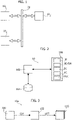
Figure 1 shows a typical electronic system; -
Figure 2 shows a typical processing system of the electronic system ofFigure 1 ; -
Figure 3 shows an embodiment of a processing system comprising a timer reference circuit configured to generating a system time signal and a circuit configured to use the system time signal; -
Figure 4 shows an embodiment of the timer reference circuit ofFigure 3 , wherein the timer reference circuit generates via a counter circuit a global reference time signal and via a time base distribution circuit a plurality of additional reference time signals; -
Figure 5 shows an embodiment of the counter circuit ofFigure 4 ; -
Figures 6A and 6B show embodiments how a processing unit of the processing system may obtain the global reference time signal or one of the additional reference time signals; -
Figures 7 and8 show embodiments of one or more circuits which use the additional reference time signals in order to store a time stamp directly at a hardware level in response to given events; -
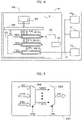
Figure 9 shows an embodiment of the time base distribution circuit ofFigure 4 ; -
Figure 10 shows a further embodiment of the timer reference circuit ofFigure 3 comprising also an extended timer circuit, an operation time counter circuit and a trigger generator circuit; -
Figure 11 shows an embodiment of a trigger generator circuit generating a trigger signal adapted to activate the extended timer circuit, operation time counter circuit and trigger generator circuit ofFigure 10 ; -
Figure 12 shows an embodiment of the extended timer circuit ofFigure 10 ; -
Figure 13 shows an embodiment of the operation of the extended timer circuit ofFigure 12 ; -
Figures 14, 15, 16 and17 shows an embodiment of the trigger generator circuit ofFigure 10 ; -
Figure 18 shows an embodiment of the operation time counter circuit ofFigure 10 ; -
Figure 19 shows an embodiment of the operation of the operation time counter circuit ofFigure 18 ; and -
Figure 20 shows an embodiment of the transmission of the additional reference time signals ofFigure 4 to one or more circuits of the processing system. - In the following description, numerous specific details are given to provide a thorough understanding of embodiments. The embodiments can be practiced without one or several specific details, or with other methods, components, materials, etc. In other instances, well-known structures, materials, or operations are not shown or described in detail to avoid obscuring aspects of the embodiments.
- Reference throughout this specification to "one embodiment" or "an embodiment" means that a particular feature, structure, or characteristic described in connection with the embodiment is included in at least one embodiment. Thus, the appearances of the phrases "in one embodiment" or "in an embodiment" in various places throughout this specification are not necessarily all referring to the same embodiment. Furthermore, the particular features, structures, or characteristics may be combined in any suitable manner in one or more embodiments.
- The headings provided herein are for convenience only and do not interpret the scope or meaning of the embodiments.
- In the following
Figures 3 to 20 parts, elements or components which have already been described with reference toFigures 1 and 2 are denoted by the same references previously used in such Figures; the description of such previously described elements will not be repeated in the following in order not to overburden the present detailed description. - As described in the forgoing with respect to
Figures 1 and 2 , in many applications, the execution of a first operation within aprocessing system 10 has to be synchronized with the execution of a second operation within thesame processing system 10 or within afurther processing system 10. - For example, in many applications the data/message exchange with one or more of the
resources 106 of theprocessing system 10, which e.g. may include information such as status data, sensor data, actuator commands, etc., should be linked to some kind of time reference/time stamp. For a temporal correlation of these functions/operations a common time base is thus required. For example, the conventional approach to this request consists in implementing some time reference within eachprocessing systems 10 configured to execute synchronized operations, wherein the time reference circuit provides a global system time for therespective processing system 10. For example, this internal time reference circuit may be implemented with a timer circuit or a real-time-clock. - For example, a
processing system 10 may acquire sensor data from a sensor via an analog-to-digital converter, ADC (see also block AD inFigure 2 ). Typically, for this purpose, the ADC is configured to generate an interrupt for theprocessing unit 102 when the A/D conversion is completed. In response to this interrupt, theprocessing unit 102, such as a microprocessor programmed via software instructions, may read the digital sample provided by the ADC and read also the global system time from the reference circuit, thereby associating a sampling time/time stamp with the digital sample for the sensor data. Similar interrupts indicating given events, which should then be associated with a given time stamp, may also be generated byother resources 106 of theprocessing system 10, such as a communication interface generating an interrupt on reception of a message (such as a status message or an actuation command), a timer circuit, etc. - The time stamping, i.e. the acquiring of the global system time and association of this time to a given event, may thus be performed by the
processing unit 102, e.g. via software instructions, e.g. by means of an operating system installed on theprocessing unit 102. However, such software generated time stamps associated with given events/interrupts signaled by one or more of theresources 106 may have only a coarse accuracy related to the point of time when the event/interrupt has been received or generated, e.g. because they need to be transferred first through several software layers before a software time stamp is added. This delay may thus have a negative impact on the real-time behavior of the overall system and therefore the delay and the variation on the delay should be as small as possible. -
Figure 3 shows an embodiment of aprocessing system 10a in accordance with the present description. - In the embodiment considered, the
processing system 10a comprises atime reference circuit 122 configured to generate a time reference signal GST, which is provided to a plurality ofcircuits 110 of theprocessing system 10a. Generally, thecircuit 110 may be any circuit of theprocessing 10a requiring a reference time. For example, reference can be made to the description of theprocessing system 10 shown inFigure 2 . For example, thecircuit 110 may be aprocessing unit 102 or one of theresources 106 shown inFigure 2 . Preferably, thetime reference circuit 122 and the circuit(s) 110 are integrated in the same integrated circuit. - Specifically, in the embodiment considered, the
time reference circuit 122 is configured to generate the signal GST in response to a clock signal CLK provided by anoscillator circuit 120. Generally, theoscillator circuit 120 may be integrated in the integrated circuit of theprocessing system 10a or may be at least in part be connected to a pin of the integrated circuit of theprocessing system 10a. For example, in various embodiments, theoscillator circuit 120 may be implemented with an external reference oscillator and an internal phase-locked loop (PLL). - Thus, generally, the
time reference circuit 122 receives at input a clock signal CLK and generates the time reference signal GST. Specifically, in various embodiments, the time reference signal GST is not a mere binary trigger signal but corresponds to a data signal having a plurality of bits, wherein the value of the time reference signal GST represents a system time. For example, the time reference signal GST may have 32 or 64 bits. - Specifically, in various embodiments, the
circuit 122 is configured to increase the time reference signal GST in response to the clock signal CLK, such that the time reference signal GST corresponds to the number of "ticks" that have transpired since a given starting date, usually called epoch. Generally, the epoch may be a fixed date, e.g. 1 January 1970 00:00:00 UT similar to the Unix system time or 1 January 1601 00:00:00 UT similar to a Windows based system time, or variable, e.g. from the switch on of theprocessing system 10a. - For example, reference can be made to the webpage https://en.wikipedia.org/wiki/System_time for possible encoding schemes of a system time, which may also be applied to the time reference signal GST.
- Accordingly, from a circuit point of view, each tick determined as a function of the clock signal CLK corresponds to a given period/time, such as 100 ns or 1 ms, and the (count) value of the signal GST may be used, e.g., to trigger given operations within the
circuits 110. Moreover, by synchronizing the value of the signal GST betweenplural processing systems 10a (e.g. by using an interface IF shown inFigure 2 and thecommunication system 20 shown inFigure 1 ) and by using the same time resolution for the ticks in thevarious processing systems 10a, the operation of theseprocessing systems 10a may be synchronized. - As mentioned before, the signal GST is provided to a plurality of
circuits 110 of theprocessing system 10a. Specifically, in various embodiments the signal GST may be provided in reduced resolution to thecircuits 110. - For example,
Figure 4 shows an embodiment of such atime reference circuit 122. - Specifically, as described, in the foregoing the
time reference circuit 122 is configured to increase a count value. For example, inFigure 4 is schematically shown acounter circuit 124, configured to increase the signal GST in response to the clock signal CLK. - For example,
Figure 5 shows a possible embodiment of thecounter circuit 124. - In the embodiment considered, the
counter circuit 124 comprises adigital counter circuit 1242 configured to increase the value of the signal GST by a given amount INC in response to a clock signal NSC_CLK, e.g. at each rising or falling edge of the clock signal NSC_CLK thedigital counter circuit 1242 increase the value of the count value (signal GST) by the value INC. For example, in the embodiment considered, thedigital counter circuit 1242 comprises: - a
register 1248 configured to store the count value (signal GST); and - a
digital adder circuit 1246 configured to sum the count value (signal GST) provided by theregister 1248 and the signal INC, wherein the result is again stored to theregister 1248 in response to the clock signal NSC_CLK. - In various embodiments, the signal INC is programmable and may be stored for this purpose in a
register 1244. In various embodiments, the content of theregister 1244 is programmable, e.g. by means of theprocessing unit 102, e.g. via software instructions. For example, in various embodiments, the value of the signal INC is determined as a function of the frequency of the clock signal NSC_CLK in order to implement ananosecond counter 124. For example, for this purpose, the signal GST may have 64 bits, and for usual clock signals (e.g. in a range between 10MHz and 100MHz), the signal INC may only have 16 bits. - In various embodiments, the content of the
register 1248, i.e. the signal GST, may be readable by theprocessing unit 102, e.g. via software instructions. Moreover, also the content of theregister 1248 may be writeable/programmable, e.g. by means of theprocessing unit 102, e.g. via software instructions. For example, in this way, theprocessing unit 102 may set an initial value of theregister 1248/signal GST. In fact, after start-up the signal GST indicates essentially the time elapsed since theprocessing system 10a has been switched on. Conversely, by overwriting the content of theregister 1248 may synchronize the signal GST with respect to a starting date/epoch and/or withother processing systems 10. - As mentioned before, in various embodiments, the register may store 64 bits. However, often the
processing unit 102 may only support 32 bits read and write accesses. In this, case theprocessing unit 102 needs to execute two read or write accesses in order to read or write the content of theregister 1248. However, in the meantime the content of theregister 1248 may already change. - Accordingly, in various embodiments, the
counter circuit 124 may comprise a further register or latch 1250 configured to store at least part of the content of theregister 1248 when a read or write access to the signal GST is performed. For example, once theprocessing unit 102 requests a read access to the upper or lower 32 bits of the signal GST (as indicated schematically by a signal RW), the register orlatch 1250 may store the content of all bits of the signal GST or only the respective lower or upper 32 bits of the signal GST currently not read. Next, when theprocessing unit 102 requests a read access to the remaining lower or upper 32 bits of the signal GST, the respective bits may be read from the register orlatch 1250. - Generally, the clock signal NSC_CLK may correspond directly to the clock signal CLK shown in
Figure 4 . Conversely, in the embodiment considered, thecounter circuit 124 supports a plurality of clock signals CLK1..CLKk. In this case, thecounter circuit 124 may comprise amultiplexer 1240 configured to select one of the clock signals CLK1..CLKk as clock signal NSC_CLK as a function of a selection signal CLK_SEL. In various embodiments, also the signal CLK_SEL may be programmable (e.g. be stored the value of the signal CLK_SEL in a register), e.g. by means of theprocessing unit 102, e.g. via software instructions. -
Figure 4 shows also that thetime reference circuit 122 may also comprise a timebase distribution circuit 126. Specifically, thecircuit 126 is configured to generate a plurality of time base signals TBI0..TBIn, wherein each of the time base signals TBI0..TBIn is provided to one or morerespective circuits 110 of theprocessing system 10a. - In various embodiments, one or more of the
circuits 110 may be selectable, e.g. by means of a suitable programming of theprocessing unit 102 or by means of configuration data of theprocessing system 10a which are read during the start-up of theprocessing system 10a. - For example, a time base signal TBI0 may be provided always to the
processing unit 102 and/or one or more time base signals TBI1..TBIn may be provided torespective resources 106 of theprocessing system 10a. - Accordingly, as schematically shown in
Figures 6A and 6B , in various embodiments, theprocessing unit 102 may be interfaced with thetime reference circuit 122 via two interfaces. - Specifically, as shown in
Figure 6A , theprocessing unit 102 may be connected to thetime reference circuit 122 via asystem bus 108, e.g. used to connect theresources 106 to theprocessing system 102. For example, such a system bus may include one or more Advanced Microcontroller Bus Architecture (AMBA) buses, such as an AMBA High-performance Bus (AHB). Accordingly, in various embodiments, amicroprocessor 102 may read the content of theregister 1248/signal GST via conventional software instructions, e.g. via an operating system OS of theprocessing unit 102, by using the address associated with theregister 1248/signal GST. - Conversely, a lot of modern microprocessors also include an internal Time Stamp Counter (TSC), which is e.g. included in x86 processors since the Pentium. As shown in
Figure 6B , in this case, one of the time base signal, e.g. TBI0, may correspond to the signal of the Time Stamp Counter TSC. - Substantially, while in
Figure 6A the software instruct has to access a hardware resource of theprocessing system 10a, which has to be routed through thebus system 108, the access inFigure 6B occurs to a (virtual) internal resource of themicroprocessor 102. - As described in the foregoing, one or more time base signals, e.g. TBI1..TBIn are provided to respective (e.g. programmable)
resources 106 of theprocessing system 10a. For example, this is schematically shown inFigure 7 , wherein: - a time base signal TBI1 is provided to an analog-to-digital converter ADC of the
processing system 10a; and/or - a time base signal TBI2 is provided to first communication interface IF1 of the
processing system 10a, such as a SPI interface; and/or - a time base signal TBI3 is provided to second communication interface IF2 of the
processing system 10a, such as a CAN bus interface. - Thus, in the embodiments considered, one or more of the
resource 106 of theprocessing system 10a receive directly a time base signal (TBI0..TBIn) indicative of the global system time GST. - Accordingly, these one or
more resources 106 directly store the value of the respective time base signal in response to given events, e.g. when generating a respective interrupt for theprocessing unit 102. - This is schematically shown in
Figure 7 , wherein each (or at least one) of theresources 106 receiving a time base signal comprise a respective register for storing the value of the respective time base signal, e.g.: - the analog-to-digital converter ADC may comprise a register REG1 for storing the content of the time base signal TBI1;
- the interface IF1 may comprise a register REG2 for storing the content of the time base signal TBI2; and
- the interface IF2 may comprise a register REG3 for storing the content of the time base signal TBI3.
- The
processing system 10a is thus configured that theprocessing unit 102 reads the content of these registers (REG1, REG2, REG3). Accordingly, in this way, the time stamp is stored directly at a hardware level when the respective event is generated, thereby avoiding that theprocessing unit 102 has to obtain separately, e.g. via software instructions (see alsoFigures 6A and 6B ), a respective time stamp. - For example,
Figure 8 shows a possible embodiment of the electronic system of avehicle 30. As described with respect toFigure 1 , in this case a plurality ofprocessing systems communication system 20, such as a CAN bus. - For example, in this architecture the blocks of the
processing system 10a ofFigure 7 may be integrated in an integrated circuit, wherein: - the analog-to-digital converter ADC is connected to an analog sensor AS; and/or
- the communication interface IF1 is connected to a digital sensor DS, and/or
- the communication interface IF2 is connected to the
communications system 20. - For example, in such a
processing system 10a, the analog-to-digital converter ADC may store the value of the respective time base signal TBI1 to the register REG1 when an analog-to-digital conversion has been completed. Optionally, the analog-to-digital converter ADC may generate (preferably simultaneously) an interrupt for theprocessing unit 102. - Similarly, the interface IF1 may store the value of the respective time base signal TBI2 to the register REG2 when a response has been received from the digital sensor DS. Optionally, the interface IF1 may generate (preferably simultaneously) an interrupt for the
processing unit 102. - Finally, the interface IF2 may store the value of the respective time base signal TBI3 to the register REG3 when a data-packet has been received via the
communication system 20, e.g. from anotherprocessing system 10 connected to thecommunication system 20. Optionally, the interface IF2 may generate (preferably simultaneously) an interrupt for theprocessing unit 102. - Accordingly, once the
processing unit 102 determines a given event of one of theresources 106, e.g. via a respective interrupt or by periodically reading the content of a respective status register, theprocessing unit 102 may also read (e.g. in addition to the digital sample provided by the converter ADC, the data received by the interface IF1 and/or the data received by the interface IF2) the content of the respective register having stored the time base signal when the event occurred. For example, as shown inFigure 7 , in various embodiments, theresources 106, and in particular the registers REG1, REG2, REG3 may be connected for this purpose to thebus 108. Accordingly, in various embodiments, theprocessing unit 102 may read the content of the registers REG1, REG2, REG3 via software instructions. - Generally, the various circuits 110 (processing
unit 102 and/or resources 106) may require different resolutions of the time signal GST. Accordingly, as shown inFigure 4 , each time base signal TBI0..TBIn has associated a respective timebase interface circuit 1260..126n configured to generate the respective time base signal TBI0..TBIn as a function of the signal GST. - For example, in unclaimed embodiments, each of the time base signals TBI0..TBIn is connected to a given
resource 110 of theprocessing system 10a. Thus, knowing the time resolution supported by a givenresource 110, eachresource 110 may only receive a given number of bits of the time reference signal GST. Thus, the routing of the bits may be fixed at a hardware level within each timebase interface circuit 1260..126n, e.g.: - the
processing unit 102 may receive all 64 bits of the signal GST; - the converter ADC may receive 24 bits of the signal GST;
- the interface IF1 may receive 16 bits of the signal GST; and
- the interface IF2 may receive 32 bits of the signal GST.
- Conversely,
Figure 9 shows an embodiment of a programmable timebase interface circuit 126i, which may be used for at least one of the timebase interface circuit 1260..126n. - Specifically, in the embodiment considered, the time
base interface circuit 126i receives at input the signal GST having a given number of bits N1 (e.g. 64 bits) and provides at output a respective time base signal TBIi, wherein the time base signal TBIi has the number of bits N2 (e.g. 64, 32, 24 or 16 bits) supported by therespective resource 110 connected to the time base signal TBIi. - In the embodiment considered, the time
base interface circuit 126i comprises moreover aselection circuit 1262, such as a multiplexer, configured to select for the signal TBIi N2 bits of the signal GST as a function of a selection signal CSEL. In various embodiments, the signal CSEL may be programmable (e.g. be stored the value of the signal CSEL in a register), e.g. by means of theprocessing unit 102, e.g. via software instructions. - For example, in various embodiments, the signal CSEL may have two bits and the
selection circuit 1262 may be configured to use the following mapping for the signal TBIi:N2 CSEL Selected bits of GST 16 "00" [9..24] "01" [13..28] 24 "00" [3..26] "01" [6..29] "10" [9..32] 32 "00" [3..34] "01" [6..37] "10" [9..40] 64 - [0..63] - In various embodiments, the time
base interface circuit 126i may also support one or more further reference time signals ETB0 and ETB1. For example, inFigure 9 is shown afurther multiplexer 1260 with selects as current reference time signal of the timebase interface circuit 126i one of the signals GST, ETB0 or ETB1 as a function of a selection signal SSEL, i.e. theselection circuit 1262 receives at input the current reference time signal selected by themultiplexer 1260. In various embodiments, the signal SSEL may be programmable (e.g. be stored the value of the signal SSEL in a register), e.g. by means of theprocessing unit 102, e.g. via software instructions. - Generally, in case the further reference time signal has a number of bits being smaller than the number of bits (N1) of the signal GST the missing (e.g. most significant) bits may be set to "0".
- For example,
resources 106 of aprocessing system 10a which often use an external time stamp bus may be a CAN FD (CAN with Flexible Data-Rate) interface, a sigma-delta analog-to-digital converter, a complex ADC, etc. - Generally, insofar as the further reference time signal may have a different tick time than the signal GST, also the selection implemented within the selection circuit 1262 (as a function of the selection signal CSEL) may change based on whether the reference time signal GST or a further reference time signal (ETB0, ETB1) has been selected.
- In various embodiments, the
time reference circuit 122 may also implement further functions. - For example,
Figure 10 shows an embodiment, wherein thetime reference circuit 122 may comprise (in addition to thecounter circuit 124 and the time base circuit 126) one or more of the following optional circuits: - an
extended timer circuit 128; and/or - an operation
time counter circuit 130; and/or - a
trigger generator circuit 132. - Generally, these
circuits counter circuit 124. - Specifically, in various embodiments, the trigger signal TRIG corresponds to the clock signal CLK used by the
counter circuit 124, e.g. the signal NSC_CLK shown inFigure 5 . - Conversely,
Figure 11 shows an embodiment of atrigger generator circuit 134, which may be included in thecounter circuit 124. - Specifically, in the embodiment considered, the
trigger generator circuit 134 implements a pre-scaler for the clock signal CLK/NSC_CLK used by thecounter circuit 124. For example, in the embodiment considered, thetrigger generator circuit 134 comprises for this purpose adigital counter 1342 which generates a signal COUNTER EXP INT when the counter reaches a given reference value. - For example, in various embodiments, the
counter 1342 is a down-counter which generates the signal COUNTER EXP INT when the count value of thecounter 1342 reaches 0. In this case, thecounter 1342 may be configured to set the count value again to a reload value COUNTER_RELOAD_VAL. In various embodiments, the signal COUNTER_RELOAD_VAL may be programmable (e.g. be stored the value of the signal COUNTER_RELOAD_VAL in a register), e.g. by means of theprocessing unit 102, e.g. via software instructions. - In various embodiments, the
trigger generator circuit 134 may be selectively enabled. For example, in the embodiment considered, thetrigger generator circuit 134 may be enabled by enabling thecounter 1342 via an enable signal COUNTER_EN. In various embodiments, the signal COUNTER_EN may be programmable (e.g. be stored the value of the signal COUNTER_EN in a register), e.g. by means of theprocessing unit 102, e.g. via software instructions. - Thus, the trigger signal TRIG may correspond to the signal COUNTER EXP INT which essentially is set each time the clock signal has reached a given number of COUNTER_RELOAD_VAL cycles.
- In various embodiments, the
trigger generator circuit 134 is also configured to synchronize at acircuit 1340 the clock signal CLK/NSC_CLK used by thecounter circuit 124 with an auxiliary signal AEVENT indicative of a given event, thereby generating a signal AUX_EVENT_SYNCED being set when the clock signal CLK/NSC_CLK is set and the auxiliary signal AEVENT is set. - In the embodiment considered, the
trigger generator circuit 134 may thus comprise a multiplexer configured to select for the trigger signal TRIG either the signal AUX_EVENT_SYNCED or the signal COUNTER EXP INT as a function of a selection signal EVENT_SOURCE_SEL. In various embodiments, the signal EVENT_SOURCE_SEL may be programmable (e.g. be stored the value of the signal EVENT_SOURCE_SEL in a register), e.g. by means of theprocessing unit 102, e.g. via software instructions. - Thus, in the embodiment considered, the
circuit 124 implements a Base Time Unit (BTU), which essentially comprises acounter 1242, such as a 64-bit nanosecond counter (NSC). Preferably, the time tick granularity of this counter is programmable via the signal INC and should be set based on clock signal NSC_CLK used, such that a single tick period equals to one nanosecond. For example, assuming a clock source frequency of 10MHz, the increment step INC should be (10^9/10^5) = 100 or 0x64. Conversely, the trigger/event generator 134 is configured to generate periodic pulse based on a programmable (e.g. timeout)counter 1342 which runs with the clock signal NSC_CLK. - As mentioned before, the trigger signal TRIG may be used by the
optional circuits - For example,
Figure 12 shows an embodiment of anextended timer circuit 128. - Specifically, in the embodiment considered, the
extended timer circuit 128 is implemented with acounter circuit 128 configured to generate a time signal ENTP having 80 bits, wherein the bit sequence of the lower 64 bits follows the Network Time Protocol (NTP) format, which is, e.g., described at https://en.wikipedia.org/wiki/ Network_Time_Protocol#Timestamps. - Specifically, also such a NTP format uses essentially a fist bit-sequence 1280b of 32 bits indicative of the seconds lapsed since the era epoch of 1st January 1900. Conversely, a second bit-sequence 1280c of 32 bits is indicative of the fraction of seconds. Accordingly, the 32-bit (seconds) counter 1280b would overflow in year 2036. To overcome this potential overflow the updated NTPv4 format uses 64-bit for second and 64-bit for fraction of second. But this extended range is essentially useless for
typical processing systems 10a, and accordingly only an additional 16-bit overflow counter 1280a is added in the embodiment considered, thereby using essentially a 48-bit second counter (IEEE 1588-2008 implementation). - In various embodiments, the resolution for the "fraction of seconds" stored is 1 nanosecond. Accordingly, in this case, the counter 1280c should perform a rollover when the respective count value reaches 0x3B9A_C9FF.
- In various embodiments, the
extended timer circuit 128 may be driven either via the trigger signal TRIG or directly via the clock signal CLK/NSC_CLK used by thecounter circuit 124. - Accordingly, in various embodiments, also the increment step size ExNTP_INC_STEP for the
extended timer circuit 128, in particular the counter 1280c, may be programmable, e.g. by means of theprocessing unit 102, e.g. via software instructions. For example, when theextended timer circuit 128 uses the clock signal CLK/NSC_CLK having a frequency of 100MHz, the step ExNTP_INC_STEP should be set to 10. Conversely, when theextended timer circuit 128 uses the trigger signal TRIG with a pre-scale value COUNTER_RELOAD_VAL of 4 for the same clock signal CLK/NSC_CLK (100MHz), the step size ExNTP_INC_STEP should be 40. - In various embodiments, the value of the
extended timer circuit 128 may be readable and optionally also writable by means of theprocessing unit 102, e.g. via software instructions. In case theprocessing unit 102 has less bits, e.g. only 32, theprocessing unit 102 may perform plural consecutive accesses to the values of the counter 1280a, 1280b and 1280c. Thus, also in this case may be used a register or latch to store the remaining bits as described with respect toFigure 5 for thecounter circuit 124. - Moreover, in various embodiments, the
extended timer circuit 128 may also support a synchronization operation via a synchronization signal SYNC provided by anotherNTP timer circuit 136, such as the NTP timer of an (external or internal) Ethernet MAC (IEEE 1588-2008) complaint module. - For example, a possible procedure for synchronizing the
extended timer circuit 128 is shown inFigure 13 . - After a
start step 1000, theprocessing unit 102 obtains (e.g. from the module 136) and stores at astep 1002 the 16 (MSB) bits to the counter 1280a. - At a
next step 1004, theprocessing unit 102 activates the synchronization mode of theextended timer circuit 128, e.g. by sending a suitable command to theextended timer circuit 128. Accordingly, theextended timer circuit 128 will store the signal SYNC to the lower 64 bits, i.e. will overwrite the content of the count values 1280b and 1280c. - In various embodiments, the
processing unit 102 may then obtain at astep 1006 again the 16 MSB from themodule 136 and verify at astep 1008 whether the corresponding bits provided by themodule 136 changed, e.g. performed an overflow. - In case the bits changed (output "N" of the verification step 1008), the
processing unit 102 may return to thestep 1002 for performing a new synchronization operation. - Conversely, in case the bits did not change (output "Y" of the verification step 1008), the procedure ends at a
stop step 1010. - As mentioned before, the
time reference circuit 122 may also comprise an optionaltrigger generator circuit 132. For example,Figure 14 shows a possible implementation of thetrigger generator circuit 132. - Specifically, in the embodiment considered, the
trigger generator circuit 132 receives at input the trigger signal TRIG and generates one or more trigger signals TRIG0..TRIGm. - For example, in the embodiment considered, the
trigger generator circuit 132 comprises at least onetrigger generator sub-circuit 1320..132m, wherein each trigger generator sub-circuit is configured to generate one or more respective trigger signals TRIG0..TRIGm. - For example,
Figure 15 shows a possible embodiment of a generic trigger generator sub-circuit 132i. - In the embodiment considered, the trigger generator sub-circuit 132i essentially comprises a
digital counter 1322 configured to increase a respective count value in response to the trigger signal TRIG and the trigger generator sub-circuit 132i is configured to set one or more respective trigger signals TRIGi as a function of the count value of thecounter 1322. - In various embodiments, the
counter 1322 does not receive directly the trigger signal TRIG, but the signal TRIG is provided to a further programmablepre-scale circuit 1320 and thecounter 1322 is increased in response to the pre-scaled trigger signal TRIG. The respective description of the pre-scale circuit 1342 (seeFigure 11 ) applies also to thepre-scale circuit 1320. - Accordingly, in various embodiments, each trigger generator sub-circuit 132i may comprise a respective
pre-scale circuit 1320 andcounter 1322. - As mentioned before the one or more trigger signals TRIGi of a given trigger generator sub-circuit 132i are generated as a function of the count value of the
respective counter 1322. -
Figures 16 and17 show in this respect two embodiment which may be implemented alternatively or also in combination (e.g. by using a respective mode selection signal). - Specifically,
Figure 16 shows an embodiment, wherein the trigger generator sub-circuit 132i is operated as a timeout counter configured to generate a signal RE when thecounter 1322 has counted for a given number of cycles. - For example, in the embodiment considered, the
counter 1322 is operated as a up or down counter and when thecounter 1322 reaches a given value (e.g. 0x0000 0000 or 0xFFFF FFFF for a 32 bit counter), thecounter 1322 loads a given reload value REL_VAL and generates a reload signal RE. In various embodiments, the signal REL_VAL may be programmable (e.g. be stored the value of the signal REL_VAL in a register 1324), e.g. by means of theprocessing unit 102, e.g. via software instructions. Similarly, also the count direction (up or down) of thecounter 1322 may be programmable. - Accordingly, in the embodiment considered, the trigger signal TRIGi may correspond to the reload signal RE. In the embodiment considered, the reload signal RE is also stored to a
status register 1326 of the trigger generator sub-circuit 132i. - Conversely,
Figure 17 shows an embodiment, wherein the trigger generator sub-circuit 132i is operated as a compare module. - Specifically, in the embodiment considered, the
counter 1322 is again reset to a given start value (typically 0) and thecounter 1322 is activated, thereby varying the respective count value. For example, in various embodiments, thecounter 1322 may be reset and started via theprocessing unit 102, e.g. via software instructions. In various embodiments, the count direction (up or down) of thecounter 1322 may be programmable. - In the embodiment the count value of the
counter 1322 is provided to one ormore comparators 1330. For example inFigure 17 are shown fourcomparators 13300..13303. Each of thecomparators 13300..13303 is configured to compare the count value of thecounter 1322 with a respective comparison value COMP_VAL0..COMP_VAL3. In various embodiments, the comparison values COMP_VAL0..COMP_VAL3 may be programmable (e.g. be stored the comparison values COMP_VAL0..COMP_VAL3 inrespective registers 13280..13283), e.g. by means of theprocessing unit 102, e.g. via software instructions. - Accordingly, in the embodiment considered, each of the
comparators 13300..13303 may generate a respective trigger signal TRIGi0..TRIGi3 when the count value of thecounter 1322 corresponds to the respective comparison value COMP_VAL0..COMP_VAL3. In the embodiment considered, the values of the trigger signals TRIGi0..TRIGi3 are also stored to respective bits CMP0..CMP3 of astatus register 1326 of the trigger generator sub-circuit 132i. - Generally, the trigger signals provided by the trigger generator sub-circuit 132i may thus be used in various modes, such as:
- a mere flags which are stored to a
status register 1326 of the trigger generator sub-circuit 132i; - generate an interrupt for the
processing unit 102; - generate trigger signals/interrupts for
other resources 106 of theprocessing system 10a, such as starting an A/D conversion, obtaining sensor data from a digital sensor, etc. - In various embodiments, each of the trigger generator sub-circuit 132i may also be associated with a given circuit 110 (processing
unit 102 or resource 106) of theprocessing system 10a. - In various embodiments, the use of the trigger signal, such as simple storage to the
status register 1326 or also the generation of an interrupt for theprocessing unit 102 may be programmable. - As mentioned before, in various embodiments, the
time reference circuit 122 may also comprise an operationtime counter circuit 130. For example,Figure 18 shows an embodiment of the operationtime counter circuit 130. - In the embodiment considered, the operation
time counter circuit 130 comprises at least one counter 13020..1302l, wherein each counter 13020..1302l is configured to generate a respective count value OTC0..OTCl, which may be read (and possibly also written) via theprocessing unit 102, e.g. via software instructions. Moreover, in various embodiments, each of the counter 13020..1302l may be reset and/or started and/or stopped by theprocessing unit 102, e.g. via software instructions. - Generally, each of the counters 13020..1302l may have essentially the architecture of the
counter 1242 shown inFigure 5 (possibly also comprising the register or latch 1250 for improving the read access to the count value). In fact, also in this case, each of the counters 13020..1302l is configured to increase the respective count value by a given increase rate, which is programmable via theprocessing unit 102, e.g. via software instructions. - Accordingly, with respect to the
counter circuit 124 shown inFigure 5 , each of the counters 13020..1302l operates in response to the trigger signal TRIG and not directly the clock signal NSC_CLK. However, as also described with respect to the to theextended time circuit 128, in various embodiments also the clock source for the counter 13020..1302l may be chosen between the clock signal NSC_CLK or the trigger signal TRIG. Thus, by setting/programming the increase rate in an appropriate manner, also the counters 13020..1302l may be used as nanoseconds counters (similar to the extended time circuit 128). - For example, the counters 13020..1302l may be used to monitor the operating time of given application executed by the
processing unit 102. - In various embodiments, the counters 13020..1302l are configured to preserve the respective count values and configuration also over functional reset. For example, this is schematically shown in
Figure 19 . - Specifically, in response to a power-on reset or destructive reset at a
step 2000, theprocessing unit 102 may configure at astep 2004 one (or more) of the counter(s) 13020..1302l. For example, theprocessing unit 102 may read a given initial count value from anon-volatile memory 104 of theprocessing system 10a and write the initial count value to the selected counter 13020..1302l. - Accordingly, the selected counter 13020..1302l will wait at a
step 2006 for a new count event (as indicated by the trigger signal TRIG or the clock signal NSC_CLK). Specifically, in the absence of a count event (output "N" of the step 2006), the counter returns to thestep 2006. Conversely, when a count event is signaled (output "Y" of the step 2006), the counter increases at astep 2008 the count value. - As schematically shown in
Figure 19 , in various embodiments, theprocessing unit 102 may periodically store the count value of the selected counter 13020..1302l. For example, for this purpose theprocessing unit 102 may verify at astep 2010 whether a given store interval has lapsed. In case the store interval has not elapsed (output "N" of the step 2010), the procedure returns to thestep 2006. Conversely, in case store interval has elapsed (output "Y" of the step 2010), theprocessing unit 102 may overwrite at astep 2012 the initial count value in thenon-volatile memory 104 of theprocessing unit 10a with the current count value of the selected counter 13020..13021, and the procedure returns to thestep 2012. - Accordingly, by storing the count value to a
non-volatile memory 104 and reprogramming the count value to the selected counter 13020..13021, the count value may be conserved also after a power-on/destructive reset. - Conversely, when a function reset occurs at a
step 2002, the counters 13020..1302l may already preserve the respective count values and configuration. Accordingly, in this case thestep 2004 may be omitted, i.e. the procedure may directly proceed to thestep 2006. - In various embodiments, one or more of the time reference signals (global system time GST and/or the time reference signals TBI0..TBIn) may be transmitted in encoded format.
- For example, this is schematically shown in
Figure 20 for the time reference signals TBI0..TBIn. Specifically, as described with respect toFigure 4 , each of the timebase interface circuit 1260..126n is configured to generate a respective time reference signals TBI0..TBIn, which is provided to arespective circuit 1100..110n (processingunit 102 or resource 106) . - In the embodiment considered, the reference signals TBI0..TBIn are not transmitted directly to the
respective circuit 110, but each timebase interface circuit 1260..126n provides the respective time reference signal TBI0..TBIn to anencoder circuit 1380..138n, thereby generating respective encoded time reference signals. Next, eachencoder circuit 1380..138n transmits the respective encoded time reference signal via arespective communication channel 1420..142n to arespective decoder circuit 1400..140n. Finally, thedecoder circuits 1400..140n decode the respective received encoded time reference signal and provided the decoded time reference signal to therespective circuit 1100..110n. - For example, the encoder and
decoder circuit 1380..138n and 1400..140n may be: - Gray code encoders and decoders;
- error detection and possibly correction encoders and decoders.
- Accordingly, the various solutions described in the foregoing may have one or more of the following features:
- the
counter circuit 124 may be used to implement a nanosecond counter (see e.g.Figure 5 ); - a plurality of additional reference time signals TBI0..TBIn may be generated by the
circuit 126, which may be used by one ormore resources 106 of theprocessing system 10a in order to directly store at a hardware level a value indicative of the count value of thecounter circuit 124 when given events are detected in the respective resource 106 (see e.g.Figures 6B and 7 ) ; - the additional reference time signals TBI0..TBIn may have a programmable width and/or resolution (see e.g.
Figure 9 ); - the additional reference time signals TBI0..TBIn may operate with different clock signal (see e.g.
Figure 11 ); - an
extended NTP timer 128 may be used which provides the seconds (and fractions of seconds) passed since January 1, 1900 (see e.g.Figure 12 ); - one or more (operational) time counters 13020..1302l may record the execution or lifetime of applications executed by the processing unit 102 (see e.g.
Figures 18 and19 ); . - the
trigger generator circuits 1320..132m may be used to generate periodic interrupts for theprocessing unit 102 or the resources 106 (see e.g.Figure 16 ); - the
trigger generator circuits 1320..132m may be used to generate interrupts when the counter value reaches given comparison values (see e.g.Figure 17 ). - Accordingly, the solutions disclosed herein uses a high resolution (64-bit) global system time GST, which is provided at a hardware level to the
processing unit 102 and/or (in reduced resolution) to one ormore resources 106 of theprocessing system 10a, which thus may store a time stamp in response to given events. This feature enables (e.g. the operating system of) theprocessing unit 102 to obtain accurate hardware based time stamps instead of coarse software based time stamps. In fact, the captured hardware based time stamp values have a very short and constant delay versus the event which have triggered the time stamp capturing. The time at which theprocessing unit 102 is processing the hardware time stamp values has thus no influence any more on the accuracy of the time stamp information. - Of course, without prejudice to the principle of the invention, the details of construction and the embodiments may vary widely with respect to what has been described and illustrated herein purely by way of example, without thereby departing from the scope of the present invention, as defined by the ensuing claims.
Claims (14)
- A processing system (10a) comprising:- a digital processing unit (102) programmable as a function of a firmware stored to a non-volatile memory (104);- a first resource (106; ADC) and a second resource (106; IF1) connected to said digital processing unit (102) via a communication system (108), wherein said first resource (106; ADC) comprises a first register (REG1) and said second resource (106; IF1) comprises a second register (REG2);- a time reference circuit (122) comprising a first digital counter circuit (124) configured to generate, in response to a clock signal (CLK), a system time signal (GST) comprising a plurality of bits indicative of a time tick-count;characterized in that said processing system (10a) comprises a first and a second time base distribution circuit (126) configured to generate a first time base signal (TBI1) and a second time base signal (TBI2) by selecting a respective subset of the bits of said system time signal (GST), wherein said first time base signal (TBI1) is provided to said first resource (106; ADC) and said second time base signal (TBI2) is provided to said second resource (106; IF1), wherein said first and said second time base distribution circuit (126) are configured to generate said first time base signal (TBI1) and said second time base signal (TBI21), respectively, by selecting (1262):- a respective first subset of a respective given number of bits of said system time signal (GST) when a respective selection signal (CSEL) has a first value; and- a respective second subset of the respective given number of bits of said system time signal (GST) when the respective selection signal (CSEL) has a second value, whereby a time resolution of the respective time base signal varies as a function of the respective selection signal (CSEL);wherein each of said first resource (106; ADC) and said second resource (106; IF1) is configured to:- detect a respective given event,- store the respective time base signal (TBI1, TBI2) to the respective register (REG1, REG2) in response to the respective event, and- signal the respective event to said digital processing unit (102); andwherein said digital processing unit (102) is adapted to read via said communication system (108):- in response to an event having been signaled by said first resource (106; ADC), said first time base signal (TBI1) from said first register (REG1), and- in response to an event having been signaled by said second resource (106; IF1), said second time base signal (TBI2) from said second register (REG2).
- The processing system (10a) according to Claim 1, wherein said first and said second resource (106) are selected from the list of:- a communication interface (IF), such as a Universal asynchronous receiver/transmitter, Serial Peripheral Interface Bus, Inter-Integrated Circuit, Controller Area Network bus or Ethernet interface, or a debug interface;- an analog-to-digital converter (AD) or a digital-to-analog converters (DA);- a digital component (DC), such as a hardware timer, counter or a cryptographic co-processor;- an analog component (AC), such as a comparator or sensor, such as a temperature sensor; and- an analog/digital mixed signal component (MSC), such as a PWM (Pulse-Width Modulation) driver.
- The processing system (10a) according to Claim 1 or Claim 2, wherein:- said first resource (106; ADC) is an analog-to-digital converter (ADC), and wherein said event corresponds to the completion of an analog-to-digital conversion; and/or- said second resource (106; IF1) is a communication interface (IF1, IF2), and wherein said event corresponds to the reception of data via said communication interface (IF1, IF2).
- The processing system (10a) according to any of the previous claims, wherein said processing system (10a) is a microcontroller, and wherein said digital processing unit (102) is a microprocessor of said microcontroller.
- The processing system (10a) according to any of the previous claims, wherein said first digital counter circuit (124) of said time reference circuit (122) is configured to generate said system time signal (GST) by increasing the value of said system time signal (GST) by a given amount (INC) in response to said clock signal (CLK).
- The processing system (10a) according to Claim 5, wherein said given amount (INC) is programmable by means of said processing unit (102).
- The processing system (10a) according to any of the previous claims, wherein said selection signals (CSEL) are programmable by means of the processing unit (102).
- The processing system (10a) according to any of the previous claims, comprising at least one of:- an extended timer circuit (128) comprising a second digital counter circuit (1280a, 1280b, 1280c) configured to generate, in response to said clock signal (CLK) or a trigger signal (TRIG) generated as a function of said clock signal (CLK), an extended system time signal (ENTP) comprising a number of bits being greater than the number of bits of said system time signal (GST), wherein said extended system time signal (ENTP) is readable by means of said digital processing unit (102); and/or- an operation time counter circuit (130) comprising a plurality of third digital counter circuits (13020..1302l) configured to generate, in response to said clock signal (CLK) or a trigger signal (TRIG) generated as a function of said clock signal (CLK), respective count values (OTC0..OTCl), wherein each of said plurality of third digital counter circuits (13020..1302l) is reset, started and stopped by said digital processing unit (102); and/or- a trigger generator circuit (132) comprising one or more fourth digital counter circuits (1322) configured to generate, in response to said clock signal (CLK) or a trigger signal (TRIG) generated as a function of said clock signal (CLK), at least one trigger signal (TRIG0..TRIGm).
- The processing system (10a) according to any of the previous claims, wherein said digital processing unit (102) is a microprocessor, wherein said time reference circuit (122) comprises a register (1248) configured to store said system time signal (GST), wherein said microprocessor (102) is connected to said time reference circuit (122) via a system bus (108), and wherein said microprocessor (102) is adapted to read the content of said register (1248) via software instructions by using an address associated with said register (1248).
- The processing system (10a) according to Claim 9, wherein said processing system (10a) comprises a further time base distribution circuit (1260) configured to generate a further time base signal (TBI0), wherein said microprocessor comprises a virtual internal Time Stamp Counter, wherein said further time base signal (TBI0) corresponds to the signal of said virtual internal Time Stamp Counter.
- The processing system (10a) according to Claim 9, wherein said register (1248) has 64 bits, wherein said microprocessor (102) only supports 32 bits read and write accesses, wherein said microprocessor (102) is configured to execute two read accesses in order to read the content of said register (1248),wherein said first digital counter circuit (124) comprises a further register or latch (1250) configured to, once the microprocessor (102) requests a read access to the upper or lower 32 bits of said system time signal (GST), store at least the respective lower or upper 32 bits of the system time signal (GST) currently not read, andwherein, when the microprocessor (102) requests a read access to the remaining lower or upper 32 bits of the system time signal (GST), the respective bits are read from said further register or latch (1250).
- An integrated circuit, such as a micro-controller, comprising a processing system (10a) according to any of Claims 1 to 11.
- A device, such as a vehicle, comprising a plurality of processing systems (10a) according to any of Claims 1 to 11.
- A method of operating a processing system (10a) according to any of Claim 1 to 11, comprising:- generating via said time reference circuit (122) said system time signal (GST);- generating via said first and said second time base distribution circuit (126) said first time base signal (TBI1) and said second time base signal (TBI2);- detecting via said first resource (106) a given event;- in response to said event, storing said first time base signal (TBI1) to said first register (REG1);- signaling said event to said digital processing unit (102); and- reading via said digital processing unit (102) said first time base signal (TBI1) from said first register (REG1).
Applications Claiming Priority (1)
| Application Number | Priority Date | Filing Date | Title |
|---|---|---|---|
| IT102019000006633A IT201900006633A1 (en) | 2019-05-08 | 2019-05-08 | PROCESSING SYSTEM, RELATED INTEGRATED CIRCUIT, DEVICE AND PROCEDURE |
Publications (2)
| Publication Number | Publication Date |
|---|---|
| EP3736657A1 EP3736657A1 (en) | 2020-11-11 |
| EP3736657B1 true EP3736657B1 (en) | 2022-07-27 |
Family
ID=67470577
Family Applications (1)
| Application Number | Title | Priority Date | Filing Date |
|---|---|---|---|
| EP20171289.0A Active EP3736657B1 (en) | 2019-05-08 | 2020-04-24 | Processing system, related integrated circuit, device and method |
Country Status (4)
| Country | Link |
|---|---|
| US (2) | US11480994B2 (en) |
| EP (1) | EP3736657B1 (en) |
| CN (2) | CN119087854A (en) |
| IT (1) | IT201900006633A1 (en) |
Families Citing this family (3)
| Publication number | Priority date | Publication date | Assignee | Title |
|---|---|---|---|---|
| IT201800005506A1 (en) * | 2018-05-18 | 2019-11-18 | PROCESSING SYSTEM, RELATED INTEGRATED CIRCUIT AND PROCEDURE | |
| US11768515B2 (en) * | 2021-02-22 | 2023-09-26 | Psemi Corporation | Optimal timer array |
| EP4239960A1 (en) * | 2022-03-03 | 2023-09-06 | STMicroelectronics S.r.l. | Processing system, related integrated circuit, system and method |
Family Cites Families (10)
| Publication number | Priority date | Publication date | Assignee | Title |
|---|---|---|---|---|
| CA2091962A1 (en) * | 1992-03-31 | 1993-10-01 | Mark L. Witsaman | Clock synchronization system |
| WO2003021439A1 (en) * | 2001-08-29 | 2003-03-13 | Analog Devices, Inc. | Methods and apparatus for improving throughput of cache-based embedded processors by switching tasks in response to a cache miss |
| SE525930C2 (en) * | 2004-07-23 | 2005-05-31 | Kvaser Consultant Ab | Modularised system for time stamping transactions, used for computer system analysis, uses module memory to store time stamps given to reference transactions |
| US7512826B2 (en) * | 2005-04-20 | 2009-03-31 | International Business Machines Corporation | Method, apparatus, and product for an efficient virtualized time base in a scaleable multi-processor computer |
| DE102006013640A1 (en) * | 2006-03-22 | 2007-09-27 | Robert Bosch Gmbh | Method and data transmission system for transferring data between the data transmission system and a host processor of a subscriber of a data transmission system |
| WO2008018264A1 (en) * | 2006-08-08 | 2008-02-14 | Shimadzu Corporation | Positron ct apparatus |
| DE102010041363A1 (en) * | 2010-09-24 | 2012-03-29 | Robert Bosch Gmbh | Apparatus and method for providing global time information in event-driven bus communication |
| US8977881B2 (en) * | 2011-08-12 | 2015-03-10 | Apple Inc. | Controller core time base synchronization |
| DE102012204586B4 (en) * | 2012-03-22 | 2025-02-27 | Bayerische Motoren Werke Aktiengesellschaft | Gateway, nodes and procedures for a vehicle |
| US8892933B2 (en) * | 2012-04-23 | 2014-11-18 | Analog Devices, Inc. | Synchronization of multiple signal converters by transmitting signal conversion data and receiving unique correction values for the respective counters through the same data interface pins |
-
2019
- 2019-05-08 IT IT102019000006633A patent/IT201900006633A1/en unknown
-
2020
- 2020-04-24 US US16/857,544 patent/US11480994B2/en active Active
- 2020-04-24 EP EP20171289.0A patent/EP3736657B1/en active Active
- 2020-05-07 CN CN202411130309.2A patent/CN119087854A/en active Pending
- 2020-05-07 CN CN202010379147.1A patent/CN111913412B/en active Active
-
2022
- 2022-09-20 US US17/933,680 patent/US11755062B2/en active Active
Also Published As
| Publication number | Publication date |
|---|---|
| IT201900006633A1 (en) | 2020-11-08 |
| US20200356134A1 (en) | 2020-11-12 |
| US20230013396A1 (en) | 2023-01-19 |
| CN111913412A (en) | 2020-11-10 |
| EP3736657A1 (en) | 2020-11-11 |
| CN119087854A (en) | 2024-12-06 |
| US11480994B2 (en) | 2022-10-25 |
| CN111913412B (en) | 2024-08-27 |
| US11755062B2 (en) | 2023-09-12 |
Similar Documents
| Publication | Publication Date | Title |
|---|---|---|
| US11755062B2 (en) | Processing system, related integrated circuit, device and method | |
| EP1690184B1 (en) | Apparatus and method for time ordering events in a system having multiple time domains | |
| US10740041B2 (en) | Processing system, related integrated circuit, device and method | |
| US11822934B2 (en) | Processing system, related integrated circuit, device and method | |
| US20120213318A1 (en) | Network Synchronized Time Base Timer | |
| US10922015B2 (en) | Processing system, related integrated circuit, device and method | |
| CN101089838A (en) | Method for implementing 12C read-write sequence | |
| EP4254130B1 (en) | Processing system, related integrated circuit, device and method | |
| US20200167220A1 (en) | Processing system, related integrated circuit, device and method | |
| US10949570B2 (en) | Processing system, related integrated circuit and method | |
| EP4254196A1 (en) | Processing system, related integrated circuit, device and method | |
| US12353880B2 (en) | One-time programmable (OTP) memory controller with a control circuit configured to assert a pre-load start signal and a pre-load end signal, related processing system, integrated circuit and method | |
| US20230073160A1 (en) | Clock generating device, controller, and storage device | |
| EP4187415B1 (en) | Processing system, related device and method for protecting latches or flip-flops of a register | |
| CN116015523A (en) | A method, device and electronic equipment for time synchronization | |
| CN116560902A (en) | Processing system, related integrated circuit and method | |
| US9501370B2 (en) | Timer module and method for testing output signals of a timer module | |
| US20250307046A1 (en) | Processing system, related integrated circuit, device and method | |
| EP4239481B1 (en) | Processing system, related integrated circuit, device and method | |
| Luo et al. | LIN flash bootloader based on UDS | |
| CN121165891A (en) | System on chip, method, apparatus and storage medium supporting time synchronization | |
| CN116893936A (en) | Processing systems, related integrated circuits, devices and methods |
Legal Events
| Date | Code | Title | Description |
|---|---|---|---|
| PUAI | Public reference made under article 153(3) epc to a published international application that has entered the european phase |
Free format text: ORIGINAL CODE: 0009012 |
|
| STAA | Information on the status of an ep patent application or granted ep patent |
Free format text: STATUS: THE APPLICATION HAS BEEN PUBLISHED |
|
| AK | Designated contracting states |
Kind code of ref document: A1 Designated state(s): AL AT BE BG CH CY CZ DE DK EE ES FI FR GB GR HR HU IE IS IT LI LT LU LV MC MK MT NL NO PL PT RO RS SE SI SK SM TR |
|
| AX | Request for extension of the european patent |
Extension state: BA ME |
|
| STAA | Information on the status of an ep patent application or granted ep patent |
Free format text: STATUS: REQUEST FOR EXAMINATION WAS MADE |
|
| 17P | Request for examination filed |
Effective date: 20210510 |
|
| RBV | Designated contracting states (corrected) |
Designated state(s): AL AT BE BG CH CY CZ DE DK EE ES FI FR GB GR HR HU IE IS IT LI LT LU LV MC MK MT NL NO PL PT RO RS SE SI SK SM TR |
|
| GRAP | Despatch of communication of intention to grant a patent |
Free format text: ORIGINAL CODE: EPIDOSNIGR1 |
|
| STAA | Information on the status of an ep patent application or granted ep patent |
Free format text: STATUS: GRANT OF PATENT IS INTENDED |
|
| INTG | Intention to grant announced |
Effective date: 20220309 |
|
| GRAS | Grant fee paid |
Free format text: ORIGINAL CODE: EPIDOSNIGR3 |
|
| GRAA | (expected) grant |
Free format text: ORIGINAL CODE: 0009210 |
|
| STAA | Information on the status of an ep patent application or granted ep patent |
Free format text: STATUS: THE PATENT HAS BEEN GRANTED |
|
| AK | Designated contracting states |
Kind code of ref document: B1 Designated state(s): AL AT BE BG CH CY CZ DE DK EE ES FI FR GB GR HR HU IE IS IT LI LT LU LV MC MK MT NL NO PL PT RO RS SE SI SK SM TR |
|
| REG | Reference to a national code |
Ref country code: CH Ref legal event code: EP |
|
| REG | Reference to a national code |
Ref country code: DE Ref legal event code: R096 Ref document number: 602020004153 Country of ref document: DE |
|
| REG | Reference to a national code |
Ref country code: AT Ref legal event code: REF Ref document number: 1507487 Country of ref document: AT Kind code of ref document: T Effective date: 20220815 |
|
| REG | Reference to a national code |
Ref country code: IE Ref legal event code: FG4D |
|
| REG | Reference to a national code |
Ref country code: LT Ref legal event code: MG9D |
|
| REG | Reference to a national code |
Ref country code: NL Ref legal event code: MP Effective date: 20220727 |
|
| PG25 | Lapsed in a contracting state [announced via postgrant information from national office to epo] |
Ref country code: SE Free format text: LAPSE BECAUSE OF FAILURE TO SUBMIT A TRANSLATION OF THE DESCRIPTION OR TO PAY THE FEE WITHIN THE PRESCRIBED TIME-LIMIT Effective date: 20220727 Ref country code: RS Free format text: LAPSE BECAUSE OF FAILURE TO SUBMIT A TRANSLATION OF THE DESCRIPTION OR TO PAY THE FEE WITHIN THE PRESCRIBED TIME-LIMIT Effective date: 20220727 Ref country code: PT Free format text: LAPSE BECAUSE OF FAILURE TO SUBMIT A TRANSLATION OF THE DESCRIPTION OR TO PAY THE FEE WITHIN THE PRESCRIBED TIME-LIMIT Effective date: 20221128 Ref country code: NO Free format text: LAPSE BECAUSE OF FAILURE TO SUBMIT A TRANSLATION OF THE DESCRIPTION OR TO PAY THE FEE WITHIN THE PRESCRIBED TIME-LIMIT Effective date: 20221027 Ref country code: NL Free format text: LAPSE BECAUSE OF FAILURE TO SUBMIT A TRANSLATION OF THE DESCRIPTION OR TO PAY THE FEE WITHIN THE PRESCRIBED TIME-LIMIT Effective date: 20220727 Ref country code: LV Free format text: LAPSE BECAUSE OF FAILURE TO SUBMIT A TRANSLATION OF THE DESCRIPTION OR TO PAY THE FEE WITHIN THE PRESCRIBED TIME-LIMIT Effective date: 20220727 Ref country code: LT Free format text: LAPSE BECAUSE OF FAILURE TO SUBMIT A TRANSLATION OF THE DESCRIPTION OR TO PAY THE FEE WITHIN THE PRESCRIBED TIME-LIMIT Effective date: 20220727 Ref country code: FI Free format text: LAPSE BECAUSE OF FAILURE TO SUBMIT A TRANSLATION OF THE DESCRIPTION OR TO PAY THE FEE WITHIN THE PRESCRIBED TIME-LIMIT Effective date: 20220727 Ref country code: ES Free format text: LAPSE BECAUSE OF FAILURE TO SUBMIT A TRANSLATION OF THE DESCRIPTION OR TO PAY THE FEE WITHIN THE PRESCRIBED TIME-LIMIT Effective date: 20220727 |
|
| REG | Reference to a national code |
Ref country code: AT Ref legal event code: MK05 Ref document number: 1507487 Country of ref document: AT Kind code of ref document: T Effective date: 20220727 |
|
| PG25 | Lapsed in a contracting state [announced via postgrant information from national office to epo] |
Ref country code: PL Free format text: LAPSE BECAUSE OF FAILURE TO SUBMIT A TRANSLATION OF THE DESCRIPTION OR TO PAY THE FEE WITHIN THE PRESCRIBED TIME-LIMIT Effective date: 20220727 Ref country code: IS Free format text: LAPSE BECAUSE OF FAILURE TO SUBMIT A TRANSLATION OF THE DESCRIPTION OR TO PAY THE FEE WITHIN THE PRESCRIBED TIME-LIMIT Effective date: 20221127 Ref country code: HR Free format text: LAPSE BECAUSE OF FAILURE TO SUBMIT A TRANSLATION OF THE DESCRIPTION OR TO PAY THE FEE WITHIN THE PRESCRIBED TIME-LIMIT Effective date: 20220727 Ref country code: GR Free format text: LAPSE BECAUSE OF FAILURE TO SUBMIT A TRANSLATION OF THE DESCRIPTION OR TO PAY THE FEE WITHIN THE PRESCRIBED TIME-LIMIT Effective date: 20221028 |
|
| PG25 | Lapsed in a contracting state [announced via postgrant information from national office to epo] |
Ref country code: SM Free format text: LAPSE BECAUSE OF FAILURE TO SUBMIT A TRANSLATION OF THE DESCRIPTION OR TO PAY THE FEE WITHIN THE PRESCRIBED TIME-LIMIT Effective date: 20220727 Ref country code: RO Free format text: LAPSE BECAUSE OF FAILURE TO SUBMIT A TRANSLATION OF THE DESCRIPTION OR TO PAY THE FEE WITHIN THE PRESCRIBED TIME-LIMIT Effective date: 20220727 Ref country code: DK Free format text: LAPSE BECAUSE OF FAILURE TO SUBMIT A TRANSLATION OF THE DESCRIPTION OR TO PAY THE FEE WITHIN THE PRESCRIBED TIME-LIMIT Effective date: 20220727 Ref country code: CZ Free format text: LAPSE BECAUSE OF FAILURE TO SUBMIT A TRANSLATION OF THE DESCRIPTION OR TO PAY THE FEE WITHIN THE PRESCRIBED TIME-LIMIT Effective date: 20220727 Ref country code: AT Free format text: LAPSE BECAUSE OF FAILURE TO SUBMIT A TRANSLATION OF THE DESCRIPTION OR TO PAY THE FEE WITHIN THE PRESCRIBED TIME-LIMIT Effective date: 20220727 |
|
| REG | Reference to a national code |
Ref country code: DE Ref legal event code: R097 Ref document number: 602020004153 Country of ref document: DE |
|
| PG25 | Lapsed in a contracting state [announced via postgrant information from national office to epo] |
Ref country code: SK Free format text: LAPSE BECAUSE OF FAILURE TO SUBMIT A TRANSLATION OF THE DESCRIPTION OR TO PAY THE FEE WITHIN THE PRESCRIBED TIME-LIMIT Effective date: 20220727 Ref country code: EE Free format text: LAPSE BECAUSE OF FAILURE TO SUBMIT A TRANSLATION OF THE DESCRIPTION OR TO PAY THE FEE WITHIN THE PRESCRIBED TIME-LIMIT Effective date: 20220727 |
|
| PLBE | No opposition filed within time limit |
Free format text: ORIGINAL CODE: 0009261 |
|
| STAA | Information on the status of an ep patent application or granted ep patent |
Free format text: STATUS: NO OPPOSITION FILED WITHIN TIME LIMIT |
|
| PG25 | Lapsed in a contracting state [announced via postgrant information from national office to epo] |
Ref country code: AL Free format text: LAPSE BECAUSE OF FAILURE TO SUBMIT A TRANSLATION OF THE DESCRIPTION OR TO PAY THE FEE WITHIN THE PRESCRIBED TIME-LIMIT Effective date: 20220727 |
|
| 26N | No opposition filed |
Effective date: 20230502 |
|
| PG25 | Lapsed in a contracting state [announced via postgrant information from national office to epo] |
Ref country code: SI Free format text: LAPSE BECAUSE OF FAILURE TO SUBMIT A TRANSLATION OF THE DESCRIPTION OR TO PAY THE FEE WITHIN THE PRESCRIBED TIME-LIMIT Effective date: 20220727 |
|
| REG | Reference to a national code |
Ref country code: CH Ref legal event code: PL |
|
| PG25 | Lapsed in a contracting state [announced via postgrant information from national office to epo] |
Ref country code: LU Free format text: LAPSE BECAUSE OF NON-PAYMENT OF DUE FEES Effective date: 20230424 |
|
| REG | Reference to a national code |
Ref country code: BE Ref legal event code: MM Effective date: 20230430 |
|
| PG25 | Lapsed in a contracting state [announced via postgrant information from national office to epo] |
Ref country code: MC Free format text: LAPSE BECAUSE OF FAILURE TO SUBMIT A TRANSLATION OF THE DESCRIPTION OR TO PAY THE FEE WITHIN THE PRESCRIBED TIME-LIMIT Effective date: 20220727 |
|
| PG25 | Lapsed in a contracting state [announced via postgrant information from national office to epo] |
Ref country code: MC Free format text: LAPSE BECAUSE OF FAILURE TO SUBMIT A TRANSLATION OF THE DESCRIPTION OR TO PAY THE FEE WITHIN THE PRESCRIBED TIME-LIMIT Effective date: 20220727 Ref country code: LI Free format text: LAPSE BECAUSE OF NON-PAYMENT OF DUE FEES Effective date: 20230430 Ref country code: FR Free format text: LAPSE BECAUSE OF NON-PAYMENT OF DUE FEES Effective date: 20230430 Ref country code: CH Free format text: LAPSE BECAUSE OF NON-PAYMENT OF DUE FEES Effective date: 20230430 |
|
| REG | Reference to a national code |
Ref country code: IE Ref legal event code: MM4A |
|
| PG25 | Lapsed in a contracting state [announced via postgrant information from national office to epo] |
Ref country code: BE Free format text: LAPSE BECAUSE OF NON-PAYMENT OF DUE FEES Effective date: 20230430 |
|
| PG25 | Lapsed in a contracting state [announced via postgrant information from national office to epo] |
Ref country code: IE Free format text: LAPSE BECAUSE OF NON-PAYMENT OF DUE FEES Effective date: 20230424 |
|
| PG25 | Lapsed in a contracting state [announced via postgrant information from national office to epo] |
Ref country code: IE Free format text: LAPSE BECAUSE OF NON-PAYMENT OF DUE FEES Effective date: 20230424 |
|
| PG25 | Lapsed in a contracting state [announced via postgrant information from national office to epo] |
Ref country code: IT Free format text: LAPSE BECAUSE OF FAILURE TO SUBMIT A TRANSLATION OF THE DESCRIPTION OR TO PAY THE FEE WITHIN THE PRESCRIBED TIME-LIMIT Effective date: 20220727 |
|
| PG25 | Lapsed in a contracting state [announced via postgrant information from national office to epo] |
Ref country code: BG Free format text: LAPSE BECAUSE OF FAILURE TO SUBMIT A TRANSLATION OF THE DESCRIPTION OR TO PAY THE FEE WITHIN THE PRESCRIBED TIME-LIMIT Effective date: 20220727 |
|
| PG25 | Lapsed in a contracting state [announced via postgrant information from national office to epo] |
Ref country code: BG Free format text: LAPSE BECAUSE OF FAILURE TO SUBMIT A TRANSLATION OF THE DESCRIPTION OR TO PAY THE FEE WITHIN THE PRESCRIBED TIME-LIMIT Effective date: 20220727 |
|
| GBPC | Gb: european patent ceased through non-payment of renewal fee |
Effective date: 20240424 |
|
| PG25 | Lapsed in a contracting state [announced via postgrant information from national office to epo] |
Ref country code: GB Free format text: LAPSE BECAUSE OF NON-PAYMENT OF DUE FEES Effective date: 20240424 |
|
| PG25 | Lapsed in a contracting state [announced via postgrant information from national office to epo] |
Ref country code: GB Free format text: LAPSE BECAUSE OF NON-PAYMENT OF DUE FEES Effective date: 20240424 |
|
| PGFP | Annual fee paid to national office [announced via postgrant information from national office to epo] |
Ref country code: DE Payment date: 20250319 Year of fee payment: 6 |
|
| PG25 | Lapsed in a contracting state [announced via postgrant information from national office to epo] |
Ref country code: CY Free format text: LAPSE BECAUSE OF FAILURE TO SUBMIT A TRANSLATION OF THE DESCRIPTION OR TO PAY THE FEE WITHIN THE PRESCRIBED TIME-LIMIT; INVALID AB INITIO Effective date: 20200424 |
|
| PG25 | Lapsed in a contracting state [announced via postgrant information from national office to epo] |
Ref country code: HU Free format text: LAPSE BECAUSE OF FAILURE TO SUBMIT A TRANSLATION OF THE DESCRIPTION OR TO PAY THE FEE WITHIN THE PRESCRIBED TIME-LIMIT; INVALID AB INITIO Effective date: 20200424 |
|
| PG25 | Lapsed in a contracting state [announced via postgrant information from national office to epo] |
Ref country code: TR Free format text: LAPSE BECAUSE OF FAILURE TO SUBMIT A TRANSLATION OF THE DESCRIPTION OR TO PAY THE FEE WITHIN THE PRESCRIBED TIME-LIMIT Effective date: 20220727 |