EP3735115A1 - Input connection device - Google Patents
Input connection device Download PDFInfo
- Publication number
- EP3735115A1 EP3735115A1 EP20158205.3A EP20158205A EP3735115A1 EP 3735115 A1 EP3735115 A1 EP 3735115A1 EP 20158205 A EP20158205 A EP 20158205A EP 3735115 A1 EP3735115 A1 EP 3735115A1
- Authority
- EP
- European Patent Office
- Prior art keywords
- circuit board
- conductive connection
- connection unit
- connection device
- power wire
- Prior art date
- Legal status (The legal status is an assumption and is not a legal conclusion. Google has not performed a legal analysis and makes no representation as to the accuracy of the status listed.)
- Granted
Links
Images




Classifications
-
- H—ELECTRICITY
- H05—ELECTRIC TECHNIQUES NOT OTHERWISE PROVIDED FOR
- H05K—PRINTED CIRCUITS; CASINGS OR CONSTRUCTIONAL DETAILS OF ELECTRIC APPARATUS; MANUFACTURE OF ASSEMBLAGES OF ELECTRICAL COMPONENTS
- H05K5/00—Casings, cabinets or drawers for electric apparatus
- H05K5/0017—Casings, cabinets or drawers for electric apparatus with operator interface units
-
- H—ELECTRICITY
- H05—ELECTRIC TECHNIQUES NOT OTHERWISE PROVIDED FOR
- H05K—PRINTED CIRCUITS; CASINGS OR CONSTRUCTIONAL DETAILS OF ELECTRIC APPARATUS; MANUFACTURE OF ASSEMBLAGES OF ELECTRICAL COMPONENTS
- H05K5/00—Casings, cabinets or drawers for electric apparatus
- H05K5/0026—Casings, cabinets or drawers for electric apparatus provided with connectors and printed circuit boards [PCB], e.g. automotive electronic control units
- H05K5/0069—Casings, cabinets or drawers for electric apparatus provided with connectors and printed circuit boards [PCB], e.g. automotive electronic control units having connector relating features for connecting the connector pins with the PCB or for mounting the connector body with the housing
-
- H—ELECTRICITY
- H05—ELECTRIC TECHNIQUES NOT OTHERWISE PROVIDED FOR
- H05K—PRINTED CIRCUITS; CASINGS OR CONSTRUCTIONAL DETAILS OF ELECTRIC APPARATUS; MANUFACTURE OF ASSEMBLAGES OF ELECTRICAL COMPONENTS
- H05K5/00—Casings, cabinets or drawers for electric apparatus
- H05K5/02—Details
- H05K5/0247—Electrical details of casings, e.g. terminals, passages for cables or wiring
-
- H—ELECTRICITY
- H05—ELECTRIC TECHNIQUES NOT OTHERWISE PROVIDED FOR
- H05K—PRINTED CIRCUITS; CASINGS OR CONSTRUCTIONAL DETAILS OF ELECTRIC APPARATUS; MANUFACTURE OF ASSEMBLAGES OF ELECTRICAL COMPONENTS
- H05K9/00—Screening of apparatus or components against electric or magnetic fields
- H05K9/0007—Casings
- H05K9/002—Casings with localised screening
- H05K9/0022—Casings with localised screening of components mounted on printed circuit boards [PCB]
Definitions
- connection device and more particularly to an input connection device applied to an electronic device for reducing the cost and the volume and improving the electromagnetic interference thereof.
- input connection device has been widely applied to a variety of electronic devices or equipment for conveying electric power or transmitting signal information from an external source to the electronic device.
- the general trends in designing electronic devices are toward minimization, high integration and low cost.
- the structure design and the practical demand of the input connection device are more difficult. Therefore, it is important to develop an input connection device with miniaturized size and low cost.
- the input connection device includes a plurality of electric connectors, a plurality of first power wires, a printed circuit board, a second power wire and a switch.
- Each electric connector is mounted on a sidewall of a cabinet of the electronic device.
- One end of each first power wire is connected with the corresponding electric connector, and the other end of each first power wire is connected with the printed circuit board, which is disposed in the cabinet.
- One end of the second power wire is connected with the printed circuit board, and the other end of the second power wire is connected with the switch. Therefore, when the electric connector receives electric power or signal information from an external source, the electric power or the signal information is transmitted from the electric connector to the switch through the first power wire, the printed circuit board and the second power wire.
- the number of the electric connectors is increased, the number of the first power wires is increased accordingly. Consequently, the cost and the volume of the input connection device are increased. Moreover, assembly method of the input connection device is complicated and wire organization is difficult because of the plurality of first power wires, and incorrect connections between the first power wires and the electric connectors may occur easily. Furthermore, the first power wire generates additional electromagnetic interference on the input connection device, which may degrade the performance of the electronic device.
- An object of the present disclosure provides an input connection device applied to an electronic device for reducing the cost and the volume and improving the electromagnetic interference thereof.
- an input connection device for an electronic device includes a mother circuit board and a cabinet having a first wall.
- the input connection device comprises an insulation housing, a conductive connection unit, a circuit board, a switch, at least one first power wire and at least one second power wire.
- the insulation housing is disposed on the first wall and comprises a main body comprising a hollow channel.
- the conductive connection unit is disposed in the hollow channel and is engaged with the insulation housing.
- the circuit board is connected with the conductive connection unit directly.
- the switch has an input part and an output part. One end of the first power wire is connected with the circuit board. The other end of the first power wire is connected with the input part of the switch.
- One end of the second power wire is connected with the output part of the switch.
- the other end of the second power wire is connected with the mother circuit board.
- an input connection device for an electronic device includes a mother circuit board and a cabinet having a first wall.
- the input connection device comprises a plurality of insulation housings, a plurality of conductive connection units, at least one circuit board, a switch, a plurality of first power wires and a plurality of second power wires.
- Each of the insulation housing is disposed on the first wall and comprises a main body comprising a hollow channel.
- Each of the conductive connection unit is disposed in the hollow channel of the corresponding insulation housing and is engaged with the corresponding insulation housing.
- the at least one circuit board is connected with the plurality of conductive connection units directly.
- the switch has an input part and an output part.
- each first power wire is connected with the circuit board.
- the other end of each first power wire is connected with the input part of the switch.
- One end of each second power wire is connected with the output part of the switch.
- the other end of each second power wire is connected with the mother circuit board.
- FIG. 1 is a schematic perspective view illustrating an input connection device according to a first embodiment of the present disclosure.
- FIG. 2 is a schematic exploded view illustrating an insulation housing, a conductive connection unit and a fastening element of the input connection device of FIG. 1 .
- the input connection device 1 is applied to an electronic device 4 for receiving electric power or signal information from an external source, for example a DC power source, and conveying the electric power or transmitting the signal information to an internal device of the electronic device 4.
- the electronic device 4 includes the input connection device 1, a mother circuit board 2 and a cabinet 3.
- the cabinet 3 has a first wall 31 and a second wall 32 connected to the first wall 31.
- the first wall 31 has an outer side 311 and an inner side 312.
- the mother circuit board 2 is disposed in the cabinet 3.
- the input connection device 1 is disposed in the cabinet 3 and electrically connected with the mother circuit board 2.
- the input connection device 1 includes an insulation housing 11, a conductive connection unit 12, a circuit board 13, a fastening element 14, at least one electronic component 15, at least one first power wire 16, a switch 17, a second power wire 18 and a first connection element 19.
- the insulation housing 11 includes a main body 111 having a hollow channel 112.
- the hollow channel 112 runs through two ends of the main body 111 so as to form two openings at two ends.
- the hollow channel 112 includes a first channel section 113 and a second channel section 114.
- the main body 111 includes an inner surface 111a, an outer surface 111b, at least one first groove 115, at least one first protrusion 116 and at least one engaging element 117.
- the first channel section 113 has an aperture greater than that of the second channel section 114 and is served as a first accommodation space for receiving a matching electric connector (not shown).
- the at least one first groove 115 is formed on the inner surface 111a of the main body 111 and located at the second channel section 114.
- the at least one first protrusion 116 is formed on the inner surface 111a of the main body 111, adjacent to the first groove 115 and located at the second channel section 114.
- the at least one engaging element 117 is formed on the outer surface 111b of the main body 111.
- the insulation housing 11 is penetrated through and fitted in a first hole 313 of the first wall 31 of the cabinet 3.
- the at least one engaging element 117 of the insulation housing 11 is engaged with the edge of the first hole 313 of the first wall 31, so that the insulation housing 11 is fixed on the first wall 31 and portion of the insulation housing 11 is exposed from the outer side 311 of the first wall 31.
- the conductive connection unit 12 is disposed in the hollow channel 112 of the main body 111 of the insulation housing 11. Preferably but not exclusively, portion of the conductive connection unit 12 is disposed in the second channel section 114 of the hollow channel 112.
- the conductive connection unit 12 includes a first end 121, a second end 122, at least one second groove 123, at least one second protrusion 124 and a second accommodation space 125.
- the at least one second groove 123 is formed on the periphery of the conductive connection unit 12 and is corresponding to the at least one first protrusion 116 of the main body 111.
- the at least one second protrusion 124 is formed on the periphery of the conductive connection unit 12 and is corresponding to the at least one first groove 115 of the main body 111.
- the second groove 123 of the conductive connection unit 12 is engaged with the first protrusion 116 of the main body 111 and the second protrusion 124 of the conductive connection unit 12 is engaged with the first groove 115 of the main body 111, so that the conductive connection unit 12 is securely fixed in the insulation housing 11.
- the first end 121 and the second end 122 of the conductive connection unit 12 are opposite to each other.
- the first end 121 of the conductive connection unit 12 is used to contact with a contact part of the matching electric connector (not shown) and is configured to receive the electric power or the signal information transmitted from the electric connector.
- the first end 121 of the conductive connection unit 12 is a female connector, and the contact part of the matching electric connector is a male connector, which matches with the female connector.
- the first end 121 of the conductive connection unit 12 is a male connector, and the contact part of the matching electric connector is a female connector, which matches with the male connector.
- the second end 122 of the conductive connection unit 12 is exposed from the inner side 312 of the first wall 31.
- the conductive connection unit 12 outputs the electric power or the signal information through the second end 122 of the conductive connection unit 12.
- the second accommodation space 125 is formed at the second end 122 of the conductive connection unit 12.
- the insulation housing 11 and the conductive connection unit 12 are formed into one piece.
- the conductive connection unit 12 is made of metal material.
- the circuit board 13 is disposed on the second end 122 of the conductive connection unit 12 and electrically connected with the second end 122 of the conductive connection unit 12 directly.
- the circuit board 13 is perpendicular to the conductive connection unit 12 and the insulation housing 11.
- the circuit board 13 has a first side 131 and a second side 132 opposite to each other.
- the second end 122 of the conductive connection unit 12 is electrically connected with a contact pad (not shown) on the first side 131 of the circuit board 13.
- the fastening element 14 is made of metal material.
- the fastening element 14 includes a first end 141 and a second end 142.
- the first end 141 of the fastening element 14 is penetrated through a hole 133 of the circuit board 13 and fitted in the second accommodation space 125 of the conductive connection unit 12. Namely, a part of the first end 141 of the fastening element 14 is disposed in the hole 133 of the circuit board 13, and the other part of the first end 141 of the fastening element 14 is engaged with the second end 122 of the conductive connection unit 12 so that the other part of the first end 141 of the fastening element 14 is fitted in the second accommodation space 125.
- the second end 141 of the fastening element 14 is disposed on the second side 132 of the circuit board 13. Consequently, the circuit board 13 is fastened on the second end 122 of the conductive connection unit 12 through the fastening element 14.
- the conductive connection unit 12 is disposed in the hollow channel 112 of the main body 111 of the insulation housing 11 before the second end 122 of the conductive connection unit 12 is connected with the circuit board 13. In other embodiment, the conductive connection unit 12 is disposed in the hollow channel 112 of the main body 111 of the insulation housing 11 after the second end 122 of the conductive connection unit 12 is connected with the circuit board 13.
- the shape of the second accommodation space 125 of the conductive connection unit 12 matches with the shape of the first end 141 of the fastening element 14 so that the first end 141 of the fastening element 14 is fixed on the second end 122 of the conductive connection unit 12.
- the at least one electronic component 15 is disposed on at least one of the first side 131 and the second side 132 of the circuit board 13.
- the electronic component 15 is disposed on the second side 132 of the circuit board 13.
- the electronic component 15 is electrically connected with the second end 122 of the conductive connection unit 12 through the circuit board 13.
- the electronic component 15 may be an EMI suppressing element, for example but not limited to a capacitor.
- the electronic component 15 is used to suppress electromagnetic interference of the conductive connection unit 12.
- one end of the first power wire 16 is electrically connected to the second side 132 of the circuit board 13, and the other end of the first power wire 16 is electrically connected with the switch 17. Consequently, the conductive connection unit 12 is electrically connected to the switch 17 through the circuit board 13 and the first power wire 16.
- the switch 17 includes a first end 171, a second end 172, an input part 173 and output part 174.
- the input part 173 and the output part 174 are located at the first end 171.
- the first end 171 of the switch 17 is exposed from the inner side 312 of the first wall 31 of the cabinet 3.
- the input part 173 is electrically connected with the other end of the first power wire 16 for receiving the electric power or the signal information from the circuit board 13.
- a part of the second end 172 of the switch 17 is penetrated through a second hole 314 of the first wall 31 to connect with the first end 171 of the switch 17.
- the other part of the second end 172 of the switch 17 is exposed from the outer side 311 of the first wall 31 of the cabinet 3 and served as a selector, such as a button or a knob switch.
- the switch 17 is turned on or turned off for selectively allowing the electric power or the signal information to be transmitted from circuit board 13 to the mother circuit board 2. Namely, when the second end 172 of the switch 17 is pressed, the switch 17 is turned on for allowing the electric power or the signal information to be transmitted from circuit board 13 to the mother circuit board 2. When the second end 172 of the switch 17 is not pressed, the switch 17 is turned off for interrupting electric power or the signal information to be transmitted from circuit board 13 to the mother circuit board 2.
- the switch 17 is a DC switch.
- the first connection element 19 is connected to the other end of the second power wire 18.
- the first connection element 19 includes a first end 191 and a second end 192 connected with each other.
- the first end 191 of the first connection element 19 is connected with the mother circuit board 2, and the second end 192 of the first connection element 19 is connected with the other end of the second power wire 18, so that the second power wire 18 is electrically connected with the mother circuit board 2 through the first connection element 19.
- the second power wire 18 is connected with the mother circuit board 2 directly and the first connection element 19 is omitted.
- the mother circuit board 2 is disposed on the inner side of the second wall 32 of the cabinet 3. Preferably but not exclusively, the mother circuit board 2 is perpendicular to the circuit board 13.
- the input connection device 1 further includes at least one current sensor 21.
- the at least one current sensor 21 is disposed on at least one of the first side 131 and the second side 132 of the circuit board 13 for sensing the current flowing through the circuit board 13.
- the current sensor 21 is disposed on the second side 132 of the circuit board 13.
- FIG. 3 is a schematic perspective view illustrating an input connection device according to a second embodiment of the present disclosure.
- the structures and functions of the input connection device 1a of this embodiment are similar to those of the first embodiment. Component parts and elements corresponding to those of the first embodiment are designated by identical numeral references, and detailed descriptions thereof are omitted.
- the second end 122 of the conductive connection unit 12 is connected with the circuit board 13 directly without any fastening element, and the second accommodation space of the conductive connection unit 12 is omitted.
- the conductive connection unit 12 includes a first end 121 and a second end 122.
- the second end 122 of the conductive connection unit 12 is electrically connected with the contact pad (not shown) of the circuit board 13 directly.
- the conductive connection unit 12 and the circuit board 13 are formed into one piece.
- the circuit board 13 is connected with the insulation housing 11.
- the second end 122 of the conductive connection unit 12 is electrically connected with the circuit board 13 through a conductive glue.
- the second end 122 of the conductive connection unit 12 is soldered on the circuit board 13.
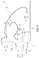
- FIG. 4 is a schematic perspective view illustrating an input connection device according to a third embodiment of the present disclosure.
- the structures and functions of the input connection device 1b of this embodiment are similar to those of the first embodiment. Component parts and elements corresponding to those of the first embodiment are designated by identical numeral references, and detailed descriptions thereof are omitted.
- the input connection device 1b further includes a second connection element 22 connected to the end of the first power wire 16.
- the second connection element 22 includes a first end 221 and a second end 222 connected with each other.
- the first end 221 of the second connection element 22 is connected with the circuit board 13 and disposed on the second side 132 of the circuit board 13.
- the second end 222 of the second connection element 22 is connected with the end of the first power wire 16, so that the first power wire 16 is connected between circuit board 13 and the switch 17 for conveying the electric power or transmitting the signal information from the circuit board 13 to the switch 17.
- FIG. 5 is a schematic perspective view illustrating an input connection device according to a fourth embodiment of the present disclosure.
- the structures and functions of the input connection device 1c of this embodiment are similar to those of the first embodiment. Component parts and elements corresponding to those of the first embodiment are designated by identical numeral references, and detailed descriptions thereof are omitted.
- the input connection device 1c includes a plurality of insulation housings 11, a plurality of conductive connection units 12, a circuit board 13, a plurality of fastening elements 14, a plurality of electronic components 15, a plurality of first power wires 16, a switch 17, a plurality of second power wires 18a and a plurality of first connection elements 19.
- the numbers of the insulation housings 11, the conductive connection units 12 and the fastening elements 14 are the same.
- the first side 31 of the cabinet 3 includes a plurality of first holes 313, and the circuit board 13 includes a plurality of holes 133.
- Each insulation housing 11 is penetrated through and fitted in the corresponding first hole 313 of the first side 31 of the cabinet 3.
- Each conductive connection unit 12 is disposed in the hollow channel 112 of the corresponding insulation housing 11.
- Each fastening element 14 is penetrated through the corresponding hole 133 of the circuit board 13 and is engaged with the second end 122 of the corresponding conductive connection unit 12.
- the plurality of electronic components 15 are disposed on the circuit board 13.
- each first power wire 16 is connected with the circuit board 13, and the other end of each first power wire 16 is connected with the input part 173 of the switch 17.
- One end of each second power wire 18 is connected with the output part 174 of the switch 17, and the other end of each second power wire 18 is connected with the mother circuit board 2.
- Each first connection element 19 is connected with the other end of the corresponding second power wire 18.
- Each second power wire 18 is connected with the mother circuit board 2 through the corresponding first connection element 19.
- FIG. 6 is a schematic perspective view illustrating an input connection device according to a fifth embodiment of the present disclosure.
- the structures and functions of the input connection device 1d of this embodiment are similar to those of the fourth embodiment. Component parts and elements corresponding to those of the fourth embodiment are designated by identical numeral references, and detailed descriptions thereof are omitted.
- the input connection device Id includes a plurality of circuit boards 13. Preferably but not exclusively, the input connection device Id includes two circuit boards 13. Each circuit board 13 includes a plurality of holes 133.
- Portion of the plurality of the conductive connection units 12 are connected with one circuit board 13, and the residue of the plurality of the conductive connection units 12 are connected with the other circuit board 13.
- Portion of the plurality of the first power wires 16 are connected with one circuit board 13, and the residue of the plurality of the first power wires 16 are connected with the other circuit board 13.
- the structures and connections of the components of the input connection device Id of this embodiment are similar to those of the fourth embodiment, and detailed descriptions thereof are omitted.
- the input connection device includes a conductive connection unit and a circuit board, and the conductive connection unit is connected with the circuit board directly without any power wire. Therefore, the cost and the volume of the input connection device are reduced, the assembly method of the input connection device is simplified and the wire organization is easier. Moreover, the electromagnetic interference of the input connection device is improved.
Landscapes
- Engineering & Computer Science (AREA)
- Microelectronics & Electronic Packaging (AREA)
- Coupling Device And Connection With Printed Circuit (AREA)
- Connections By Means Of Piercing Elements, Nuts, Or Screws (AREA)
- Shielding Devices Or Components To Electric Or Magnetic Fields (AREA)
- Handcart (AREA)
- Monitoring And Testing Of Exchanges (AREA)
Abstract
Description
- The present disclosure relates to a connection device, and more particularly to an input connection device applied to an electronic device for reducing the cost and the volume and improving the electromagnetic interference thereof.
- Nowadays, input connection device has been widely applied to a variety of electronic devices or equipment for conveying electric power or transmitting signal information from an external source to the electronic device. With increasing development of science and technology, the general trends in designing electronic devices are toward minimization, high integration and low cost. The structure design and the practical demand of the input connection device are more difficult. Therefore, it is important to develop an input connection device with miniaturized size and low cost.
- Generally, the input connection device includes a plurality of electric connectors, a plurality of first power wires, a printed circuit board, a second power wire and a switch. Each electric connector is mounted on a sidewall of a cabinet of the electronic device. One end of each first power wire is connected with the corresponding electric connector, and the other end of each first power wire is connected with the printed circuit board, which is disposed in the cabinet. One end of the second power wire is connected with the printed circuit board, and the other end of the second power wire is connected with the switch. Therefore, when the electric connector receives electric power or signal information from an external source, the electric power or the signal information is transmitted from the electric connector to the switch through the first power wire, the printed circuit board and the second power wire.
- However, if the number of the electric connectors is increased, the number of the first power wires is increased accordingly. Consequently, the cost and the volume of the input connection device are increased. Moreover, assembly method of the input connection device is complicated and wire organization is difficult because of the plurality of first power wires, and incorrect connections between the first power wires and the electric connectors may occur easily. Furthermore, the first power wire generates additional electromagnetic interference on the input connection device, which may degrade the performance of the electronic device.
- Therefore, there is a need of providing an input connection device so as to overcome the drawbacks of the conventional technologies.
- An object of the present disclosure provides an input connection device applied to an electronic device for reducing the cost and the volume and improving the electromagnetic interference thereof.
- In accordance with an aspect of the present disclosure, an input connection device for an electronic device is provided. The electronic device includes a mother circuit board and a cabinet having a first wall. The input connection device comprises an insulation housing, a conductive connection unit, a circuit board, a switch, at least one first power wire and at least one second power wire. The insulation housing is disposed on the first wall and comprises a main body comprising a hollow channel. The conductive connection unit is disposed in the hollow channel and is engaged with the insulation housing. The circuit board is connected with the conductive connection unit directly. The switch has an input part and an output part. One end of the first power wire is connected with the circuit board. The other end of the first power wire is connected with the input part of the switch. One end of the second power wire is connected with the output part of the switch. The other end of the second power wire is connected with the mother circuit board.
- In accordance with an aspect of the present disclosure, an input connection device for an electronic device is provided. The electronic device includes a mother circuit board and a cabinet having a first wall. The input connection device comprises a plurality of insulation housings, a plurality of conductive connection units, at least one circuit board, a switch, a plurality of first power wires and a plurality of second power wires. Each of the insulation housing is disposed on the first wall and comprises a main body comprising a hollow channel. Each of the conductive connection unit is disposed in the hollow channel of the corresponding insulation housing and is engaged with the corresponding insulation housing. The at least one circuit board is connected with the plurality of conductive connection units directly. The switch has an input part and an output part. One end of each first power wire is connected with the circuit board. The other end of each first power wire is connected with the input part of the switch. One end of each second power wire is connected with the output part of the switch. The other end of each second power wire is connected with the mother circuit board.
- The above contents of the present disclosure will become more readily apparent to those ordinarily skilled in the art after reviewing the following detailed description and accompanying drawings, in which:
-
-
FIG. 1 is a schematic perspective view illustrating an input connection device according to a first embodiment of the present disclosure; -
FIG. 2 is a schematic exploded view illustrating an insulation housing, a conductive connection unit and a fastening element of the input connection device ofFIG. 1 ; -
FIG. 3 is a schematic perspective view illustrating an input connection device according to a second embodiment of the present disclosure; -
FIG. 4 is a schematic perspective view illustrating an input connection device according to a third embodiment of the present disclosure; -
FIG. 5 is a schematic perspective view illustrating an input connection device according to a fourth embodiment of the present disclosure; and -
FIG. 6 is a schematic perspective view illustrating an input connection device according to a fifth embodiment of the present disclosure. - The present disclosure will now be described more specifically with reference to the following embodiments. It is to be noted that the following descriptions of preferred embodiments of this disclosure are presented herein for purpose of illustration and description only. It is not intended to be exhaustive or to be limited to the precise form disclosed.
-
FIG. 1 is a schematic perspective view illustrating an input connection device according to a first embodiment of the present disclosure.FIG. 2 is a schematic exploded view illustrating an insulation housing, a conductive connection unit and a fastening element of the input connection device ofFIG. 1 . As shown inFIGS. 1 and2 , the input connection device 1 is applied to anelectronic device 4 for receiving electric power or signal information from an external source, for example a DC power source, and conveying the electric power or transmitting the signal information to an internal device of theelectronic device 4. Theelectronic device 4 includes the input connection device 1, amother circuit board 2 and acabinet 3. Thecabinet 3 has afirst wall 31 and asecond wall 32 connected to thefirst wall 31. Thefirst wall 31 has anouter side 311 and aninner side 312. Themother circuit board 2 is disposed in thecabinet 3. The input connection device 1 is disposed in thecabinet 3 and electrically connected with themother circuit board 2. The input connection device 1 includes aninsulation housing 11, aconductive connection unit 12, acircuit board 13, afastening element 14, at least oneelectronic component 15, at least onefirst power wire 16, aswitch 17, asecond power wire 18 and afirst connection element 19. - In this embodiment, the
insulation housing 11 includes amain body 111 having ahollow channel 112. Thehollow channel 112 runs through two ends of themain body 111 so as to form two openings at two ends. Thehollow channel 112 includes afirst channel section 113 and asecond channel section 114. Themain body 111 includes aninner surface 111a, anouter surface 111b, at least onefirst groove 115, at least onefirst protrusion 116 and at least oneengaging element 117. Thefirst channel section 113 has an aperture greater than that of thesecond channel section 114 and is served as a first accommodation space for receiving a matching electric connector (not shown). The at least onefirst groove 115 is formed on theinner surface 111a of themain body 111 and located at thesecond channel section 114. The at least onefirst protrusion 116 is formed on theinner surface 111a of themain body 111, adjacent to thefirst groove 115 and located at thesecond channel section 114. The at least oneengaging element 117 is formed on theouter surface 111b of themain body 111. Theinsulation housing 11 is penetrated through and fitted in afirst hole 313 of thefirst wall 31 of thecabinet 3. The at least oneengaging element 117 of theinsulation housing 11 is engaged with the edge of thefirst hole 313 of thefirst wall 31, so that theinsulation housing 11 is fixed on thefirst wall 31 and portion of theinsulation housing 11 is exposed from theouter side 311 of thefirst wall 31. - In this embodiment, at least portion of the
conductive connection unit 12 is disposed in thehollow channel 112 of themain body 111 of theinsulation housing 11. Preferably but not exclusively, portion of theconductive connection unit 12 is disposed in thesecond channel section 114 of thehollow channel 112. Theconductive connection unit 12 includes afirst end 121, asecond end 122, at least onesecond groove 123, at least onesecond protrusion 124 and asecond accommodation space 125. The at least onesecond groove 123 is formed on the periphery of theconductive connection unit 12 and is corresponding to the at least onefirst protrusion 116 of themain body 111. The at least onesecond protrusion 124 is formed on the periphery of theconductive connection unit 12 and is corresponding to the at least onefirst groove 115 of themain body 111. When at least portion of theconductive connection unit 12 is disposed in thehollow channel 112 of themain body 111 of theinsulation housing 11, thesecond groove 123 of theconductive connection unit 12 is engaged with thefirst protrusion 116 of themain body 111 and thesecond protrusion 124 of theconductive connection unit 12 is engaged with thefirst groove 115 of themain body 111, so that theconductive connection unit 12 is securely fixed in theinsulation housing 11. Thefirst end 121 and thesecond end 122 of theconductive connection unit 12 are opposite to each other. Thefirst end 121 of theconductive connection unit 12 is used to contact with a contact part of the matching electric connector (not shown) and is configured to receive the electric power or the signal information transmitted from the electric connector. In some embodiments, thefirst end 121 of theconductive connection unit 12 is a female connector, and the contact part of the matching electric connector is a male connector, which matches with the female connector. Alternatively, thefirst end 121 of theconductive connection unit 12 is a male connector, and the contact part of the matching electric connector is a female connector, which matches with the male connector. Thesecond end 122 of theconductive connection unit 12 is exposed from theinner side 312 of thefirst wall 31. Theconductive connection unit 12 outputs the electric power or the signal information through thesecond end 122 of theconductive connection unit 12. Thesecond accommodation space 125 is formed at thesecond end 122 of theconductive connection unit 12. In some embodiments, theinsulation housing 11 and theconductive connection unit 12 are formed into one piece. Theconductive connection unit 12 is made of metal material. - In this embodiment, the
circuit board 13 is disposed on thesecond end 122 of theconductive connection unit 12 and electrically connected with thesecond end 122 of theconductive connection unit 12 directly. Preferably but not exclusively, thecircuit board 13 is perpendicular to theconductive connection unit 12 and theinsulation housing 11. Thecircuit board 13 has afirst side 131 and asecond side 132 opposite to each other. Thesecond end 122 of theconductive connection unit 12 is electrically connected with a contact pad (not shown) on thefirst side 131 of thecircuit board 13. In this embodiment, thefastening element 14 is made of metal material. Thefastening element 14 includes afirst end 141 and asecond end 142. Thefirst end 141 of thefastening element 14 is penetrated through ahole 133 of thecircuit board 13 and fitted in thesecond accommodation space 125 of theconductive connection unit 12. Namely, a part of thefirst end 141 of thefastening element 14 is disposed in thehole 133 of thecircuit board 13, and the other part of thefirst end 141 of thefastening element 14 is engaged with thesecond end 122 of theconductive connection unit 12 so that the other part of thefirst end 141 of thefastening element 14 is fitted in thesecond accommodation space 125. Thesecond end 141 of thefastening element 14 is disposed on thesecond side 132 of thecircuit board 13. Consequently, thecircuit board 13 is fastened on thesecond end 122 of theconductive connection unit 12 through thefastening element 14. - In an embodiment, the
conductive connection unit 12 is disposed in thehollow channel 112 of themain body 111 of theinsulation housing 11 before thesecond end 122 of theconductive connection unit 12 is connected with thecircuit board 13. In other embodiment, theconductive connection unit 12 is disposed in thehollow channel 112 of themain body 111 of theinsulation housing 11 after thesecond end 122 of theconductive connection unit 12 is connected with thecircuit board 13. - In an embodiment, a first screw thread is formed on the outer surface of the
first end 141 of thefastening element 14. A second screw thread is formed on the inner surface of thesecond end 122 of theconductive connection unit 12. Namely, the second screw thread is formed on the surface of thesecond accommodation space 125. The second screw thread of theconductive connection unit 12 is engaged with the first screw thread of thefastening element 14 so that thefastening element 14 is fixed on theconductive connection unit 12. Consequently, thecircuit board 13 is fastened on thesecond end 122 of theconductive connection unit 12 through thefastening element 14. In other embodiment, the shape of thesecond accommodation space 125 of theconductive connection unit 12 matches with the shape of thefirst end 141 of thefastening element 14 so that thefirst end 141 of thefastening element 14 is fixed on thesecond end 122 of theconductive connection unit 12. - In this embodiment, the at least one
electronic component 15 is disposed on at least one of thefirst side 131 and thesecond side 132 of thecircuit board 13. Preferably, theelectronic component 15 is disposed on thesecond side 132 of thecircuit board 13. Theelectronic component 15 is electrically connected with thesecond end 122 of theconductive connection unit 12 through thecircuit board 13. Theelectronic component 15 may be an EMI suppressing element, for example but not limited to a capacitor. Theelectronic component 15 is used to suppress electromagnetic interference of theconductive connection unit 12. - In this embodiment, one end of the
first power wire 16 is electrically connected to thesecond side 132 of thecircuit board 13, and the other end of thefirst power wire 16 is electrically connected with theswitch 17. Consequently, theconductive connection unit 12 is electrically connected to theswitch 17 through thecircuit board 13 and thefirst power wire 16. Theswitch 17 includes afirst end 171, asecond end 172, aninput part 173 andoutput part 174. Theinput part 173 and theoutput part 174 are located at thefirst end 171. Thefirst end 171 of theswitch 17 is exposed from theinner side 312 of thefirst wall 31 of thecabinet 3. Theinput part 173 is electrically connected with the other end of thefirst power wire 16 for receiving the electric power or the signal information from thecircuit board 13. A part of thesecond end 172 of theswitch 17 is penetrated through asecond hole 314 of thefirst wall 31 to connect with thefirst end 171 of theswitch 17. The other part of thesecond end 172 of theswitch 17 is exposed from theouter side 311 of thefirst wall 31 of thecabinet 3 and served as a selector, such as a button or a knob switch. Theswitch 17 is turned on or turned off for selectively allowing the electric power or the signal information to be transmitted fromcircuit board 13 to themother circuit board 2. Namely, when thesecond end 172 of theswitch 17 is pressed, theswitch 17 is turned on for allowing the electric power or the signal information to be transmitted fromcircuit board 13 to themother circuit board 2. When thesecond end 172 of theswitch 17 is not pressed, theswitch 17 is turned off for interrupting electric power or the signal information to be transmitted fromcircuit board 13 to themother circuit board 2. Preferably but not exclusively, theswitch 17 is a DC switch. - In this embodiment, one end of the
second power wire 18 is electrically connected with theoutput part 174 of theswitch 17, and the other end of thesecond power wire 18 is electrically connected with themother circuit board 2. Consequently, the electric power or the signal information transmitted from theswitch 17 is transmitted to themother circuit board 2. In this embodiment, thefirst connection element 19 is connected to the other end of thesecond power wire 18. Thefirst connection element 19 includes afirst end 191 and asecond end 192 connected with each other. Thefirst end 191 of thefirst connection element 19 is connected with themother circuit board 2, and thesecond end 192 of thefirst connection element 19 is connected with the other end of thesecond power wire 18, so that thesecond power wire 18 is electrically connected with themother circuit board 2 through thefirst connection element 19. In some embodiments, thesecond power wire 18 is connected with themother circuit board 2 directly and thefirst connection element 19 is omitted. - The
mother circuit board 2 is disposed on the inner side of thesecond wall 32 of thecabinet 3. Preferably but not exclusively, themother circuit board 2 is perpendicular to thecircuit board 13. - In some embodiments, the input connection device 1 further includes at least one
current sensor 21. The at least onecurrent sensor 21 is disposed on at least one of thefirst side 131 and thesecond side 132 of thecircuit board 13 for sensing the current flowing through thecircuit board 13. Preferably, thecurrent sensor 21 is disposed on thesecond side 132 of thecircuit board 13. -
FIG. 3 is a schematic perspective view illustrating an input connection device according to a second embodiment of the present disclosure. The structures and functions of theinput connection device 1a of this embodiment are similar to those of the first embodiment. Component parts and elements corresponding to those of the first embodiment are designated by identical numeral references, and detailed descriptions thereof are omitted. Different from the input connection device 1 ofFIGS. 1 and2 , in this embodiment as shown inFIG. 3 , thesecond end 122 of theconductive connection unit 12 is connected with thecircuit board 13 directly without any fastening element, and the second accommodation space of theconductive connection unit 12 is omitted. Theconductive connection unit 12 includes afirst end 121 and asecond end 122. Thesecond end 122 of theconductive connection unit 12 is electrically connected with the contact pad (not shown) of thecircuit board 13 directly. Preferably, theconductive connection unit 12 and thecircuit board 13 are formed into one piece. When portion of theconductive connection unit 12 is disposed in thehollow channel 112 of themain body 111 of theinsulation housing 11, thecircuit board 13 is connected with theinsulation housing 11. In some embodiments, thesecond end 122 of theconductive connection unit 12 is electrically connected with thecircuit board 13 through a conductive glue. In some other embodiments, thesecond end 122 of theconductive connection unit 12 is soldered on thecircuit board 13. -
FIG. 4 is a schematic perspective view illustrating an input connection device according to a third embodiment of the present disclosure. The structures and functions of theinput connection device 1b of this embodiment are similar to those of the first embodiment. Component parts and elements corresponding to those of the first embodiment are designated by identical numeral references, and detailed descriptions thereof are omitted. Different from the input connection device 1 ofFIGS. 1 and2 , in this embodiment as shown inFIG. 4 , theinput connection device 1b further includes asecond connection element 22 connected to the end of thefirst power wire 16. Thesecond connection element 22 includes afirst end 221 and asecond end 222 connected with each other. Thefirst end 221 of thesecond connection element 22 is connected with thecircuit board 13 and disposed on thesecond side 132 of thecircuit board 13. Thesecond end 222 of thesecond connection element 22 is connected with the end of thefirst power wire 16, so that thefirst power wire 16 is connected betweencircuit board 13 and theswitch 17 for conveying the electric power or transmitting the signal information from thecircuit board 13 to theswitch 17. -
FIG. 5 is a schematic perspective view illustrating an input connection device according to a fourth embodiment of the present disclosure. The structures and functions of theinput connection device 1c of this embodiment are similar to those of the first embodiment. Component parts and elements corresponding to those of the first embodiment are designated by identical numeral references, and detailed descriptions thereof are omitted. Different from the input connection device 1 ofFIGS. 1 and2 , in this embodiment as shown inFIG. 5 , theinput connection device 1c includes a plurality ofinsulation housings 11, a plurality ofconductive connection units 12, acircuit board 13, a plurality offastening elements 14, a plurality ofelectronic components 15, a plurality offirst power wires 16, aswitch 17, a plurality of second power wires 18a and a plurality offirst connection elements 19. The numbers of theinsulation housings 11, theconductive connection units 12 and thefastening elements 14 are the same. Thefirst side 31 of thecabinet 3 includes a plurality offirst holes 313, and thecircuit board 13 includes a plurality ofholes 133. Eachinsulation housing 11 is penetrated through and fitted in the correspondingfirst hole 313 of thefirst side 31 of thecabinet 3. Eachconductive connection unit 12 is disposed in thehollow channel 112 of the correspondinginsulation housing 11. Eachfastening element 14 is penetrated through thecorresponding hole 133 of thecircuit board 13 and is engaged with thesecond end 122 of the correspondingconductive connection unit 12. The plurality ofelectronic components 15 are disposed on thecircuit board 13. One end of eachfirst power wire 16 is connected with thecircuit board 13, and the other end of eachfirst power wire 16 is connected with theinput part 173 of theswitch 17. One end of eachsecond power wire 18 is connected with theoutput part 174 of theswitch 17, and the other end of eachsecond power wire 18 is connected with themother circuit board 2. Eachfirst connection element 19 is connected with the other end of the correspondingsecond power wire 18. Eachsecond power wire 18 is connected with themother circuit board 2 through the correspondingfirst connection element 19. -
FIG. 6 is a schematic perspective view illustrating an input connection device according to a fifth embodiment of the present disclosure. The structures and functions of theinput connection device 1d of this embodiment are similar to those of the fourth embodiment. Component parts and elements corresponding to those of the fourth embodiment are designated by identical numeral references, and detailed descriptions thereof are omitted. Different from theinput connection device 1c ofFIG. 5 , in this embodiment as shown inFIG. 6 , the input connection device Id includes a plurality ofcircuit boards 13. Preferably but not exclusively, the input connection device Id includes twocircuit boards 13. Eachcircuit board 13 includes a plurality ofholes 133. Portion of the plurality of theconductive connection units 12 are connected with onecircuit board 13, and the residue of the plurality of theconductive connection units 12 are connected with theother circuit board 13. Portion of the plurality of thefirst power wires 16 are connected with onecircuit board 13, and the residue of the plurality of thefirst power wires 16 are connected with theother circuit board 13. The structures and connections of the components of the input connection device Id of this embodiment are similar to those of the fourth embodiment, and detailed descriptions thereof are omitted. - From the above descriptions, the present disclosure provides the input connection device applied in an electronic device. The input connection device includes a conductive connection unit and a circuit board, and the conductive connection unit is connected with the circuit board directly without any power wire. Therefore, the cost and the volume of the input connection device are reduced, the assembly method of the input connection device is simplified and the wire organization is easier. Moreover, the electromagnetic interference of the input connection device is improved.
Claims (15)
- An input connection device (1) for an electronic device (4), wherein the electronic device (4) includes a mother circuit board (2) and a cabinet (3) having a first wall (31), characterized in that the input connection device (1) comprises:an insulation housing (11) disposed on the first wall (31) and comprising a main body (111) comprising a hollow channel (112);a conductive connection unit (12) disposed in the hollow channel (112) and engaged with the insulation housing (11);a circuit board (13) connected with the conductive connection unit (12) directly;a switch (17) having an input part (173) and an output part (174);at least one first power wire (16), wherein one end of the first power wire (16) is connected with the circuit board (13), and the other end of the first power wire (16) is connected with the input part (173) of the switch (17); andat least one second power wire (18), wherein one end of the second power wire (18) is connected with the output part (174) of the switch (17), and the other end of the second power wire (18) is connected with the mother circuit board (2).
- The input connection device (1) according to claim 1, characterized in that the hollow channel (112) runs through two ends of the main body (111) and includes a first channel section (113) and a second channel section (114), and the first channel section (113) has an aperture greater than that of the second channel section (114) and is served as a first accommodation space, wherein the main body (111) further comprises:an inner surface (111a);an outer surface (111b);at least one first groove (115) formed on the inner surface (111a) of the main body (111) and located at the second channel section (114);at least one first protrusion (116) formed on the inner surface (111a) of the main body (111), adjacent to the first groove (115) and located at the second channel section (114); andat least one engaging element (117) formed on the outer surface (111b) of the main body (111),wherein the insulation housing (11) is penetrated through and fitted in a first hole (313) of the first wall (31), and the at least one engaging element (117) of the insulation housing (11) is engaged with an edge of the first hole (313) of the first wall (31), so that the insulation housing (11) is fixed on the first wall (31) and portion of the insulation housing (11) is exposed from an outer side (311) of the first wall (31).
- The input connection device (1) according to claim 2, characterized in that at least portion of the conductive connection unit (12) is disposed in the second channel section (114) of the hollow channel (112) of the main body (111), wherein the conductive connection unit (12) comprises:a first end (121);a second end (122) opposite to the first end (121);at least one second groove (123) formed on a periphery of the conductive connection unit (12) and corresponding to the at least one first protrusion (116) of the main body (111);at least one second protrusion (124) formed on the periphery of the conductive connection unit (12) and corresponding to the at least one first groove (115) of the main body (111),wherein the second groove (123) of the conductive connection unit (12) is engaged with the first protrusion (116) of the main body (111) and the second protrusion (124) of the conductive connection unit (12) is engaged with the first groove (115) of the main body (111), so that the conductive connection unit (12) is securely fixed in the insulation housing (11) and the second end (122) of the conductive connection unit (12) is exposed from an inner side (312) of the first wall (31), wherein the conductive connection unit (12) is made of metal material.
- The input connection device (1) according to claim 1, characterized in that the input connection device (1) further comprises at least one fastening element (14), wherein the circuit board (13) is connected with a second end (122) of the conductive connection unit (12) through the fastening element (14), wherein the conductive connection unit (12) further comprises a second accommodation space (125) formed at the second end (122) thereof, wherein the fastening element (14) comprises a first end (141) and a second end (142), a part of the first end (141) of the fastening element (14) is disposed in a hole (133) of the circuit board (13), and the other part of the first end (141) of the fastening element (14) is engaged with the second end (122) of the conductive connection unit (12) so that the other part of the first end (141) of the fastening element (14) is fitted in the second accommodation space (125) and the circuit board (13) is fastened on the second end (122) of the conductive connection unit (12) through the fastening element (14).
- The input connection device (1) according to claim 1, characterized in that the circuit board (13) is perpendicular to the conductive connection unit (12) and the insulation housing (11), wherein the circuit board (13) has a first side (131) and a second side (132) opposite to each other, the conductive connection unit (12) is electrically connected with a contact pad on the first side (131) of the circuit board (13), and the end of the first power wire (16) is connected to the second side (132) of the circuit board (13).
- The input connection device (1) according to claim 1, characterized in that the input connection device (1) further comprises at least one electronic component (15) disposed on the circuit board (13) and electrically connected with the conductive connection unit (12) through the circuit board (13), wherein the electronic component (15) is an EMI suppressing element.
- The input connection device (1) according to claim 1, characterized in that the switch (17) includes a first end (171) and a second end (172) connected with each other, the first end (171) of the switch (17) is exposed from an inner side (312) of the first wall (31), a part of the second end (172) of the switch (17) is penetrated through a second hole (314) of the first wall (31), the other part of the second end (172) of the switch (17) is exposed from an outer side (311) of the first wall (31) and served as a selector, and the input part (173) and the output part (174) are located at the first end (171), wherein the switch (17) is turned on or turned off for selectively allowing electric power or signal information to be transmitted from the conductive connection unit (12) to the mother circuit board (2) through the circuit board (13) and the first power wire (16).
- The input connection device (1) according to claim 1, characterized in that the input connection device (1) further comprises a first connection element (19) connected to the other end of the second power wire (18), wherein the second power wire (18) is connected with the mother circuit board (2) through the first connection element (19).
- The input connection device (1) according to claim 1, characterized in that the input connection device (1) further comprises at least one current sensor (21) disposed on the circuit board (13) for sensing current flowing through the circuit board (13).
- The input connection device (1) according to claim 1, characterized in that a second end (122) of the conductive connection unit (12) is connected with the circuit board (13) through a conductive glue or a second end (122) of the conductive connection unit (12) is soldered on the circuit board (13).
- The input connection device (1) according to claim 1, characterized in that the input connection device (1) further comprises a second connection element (22) connected to the end of the first power wire (16), wherein the first power wire (16) is connected with the circuit board (13) through the second connection element (22).
- An input connection device (1) for an electronic device (4), wherein the electronic device (4) includes a mother circuit board (2) and a cabinet (3) having a first wall (31), characterized in that the input connection device (1) comprises:a plurality of insulation housings (11), wherein each of which is disposed on the first wall (31) and comprises a main body (111) comprising a hollow channel (112);a plurality of conductive connection units (12), wherein each of which is disposed in the hollow channel (112) of the corresponding insulation housing (11) and is engaged with the corresponding insulation housing (11);at least one circuit board (13) connected with the plurality of conductive connection units (12) directly;a switch (17) having an input part (173) and an output part (174);a plurality of first power wires (16), wherein one end of each first power wire (16) is connected with the circuit board (13), and the other end of each first power wire (16) is connected with the input part (173) of the switch (17); anda plurality of second power wires (18), wherein one end of each second power wire (18) is connected with the output part (174) of the switch (17), and the other end of each second power wire (18) is connected with the mother circuit board (2).
- The input connection device (1) according to claim 12, characterized in that the at least one circuit board (13) comprises two circuit boards (13).
- The input connection device (1) according to claim 12, characterized in that the input connection device (1) further comprises a plurality of fastening elements (14) and a plurality of electronic components (15), wherein a second end (122) of each conductive connection unit (12) is connected with the circuit board (13) through the corresponding fastening element (14), wherein the electronic components (15) disposed on the circuit board (13) and electrically connected with the plurality of conductive connection units (12) through the circuit board (13), wherein the electronic component (15) is an EMI suppressing element or a current sensor, wherein the switch (17) is a DC switch.
- The input connection device (1) according to claim 12, characterized in that a second end (122) of each conductive connection unit (12) is connected with the circuit board (13) through a conductive glue or a second end (122) of each conductive connection unit (12) is soldered on the circuit board (13).
Applications Claiming Priority (2)
| Application Number | Priority Date | Filing Date | Title |
|---|---|---|---|
| US201962842632P | 2019-05-03 | 2019-05-03 | |
| CN201910616740.0A CN111883956B (en) | 2019-05-03 | 2019-07-09 | Input connecting device |
Publications (3)
| Publication Number | Publication Date |
|---|---|
| EP3735115A1 true EP3735115A1 (en) | 2020-11-04 |
| EP3735115B1 EP3735115B1 (en) | 2023-06-07 |
| EP3735115B9 EP3735115B9 (en) | 2023-08-23 |
Family
ID=69784034
Family Applications (1)
| Application Number | Title | Priority Date | Filing Date |
|---|---|---|---|
| EP20158205.3A Active EP3735115B9 (en) | 2019-05-03 | 2020-02-19 | Input connection device |
Country Status (4)
| Country | Link |
|---|---|
| US (1) | US11122699B2 (en) |
| EP (1) | EP3735115B9 (en) |
| JP (1) | JP6876177B2 (en) |
| ES (1) | ES2948403T3 (en) |
Citations (5)
| Publication number | Priority date | Publication date | Assignee | Title |
|---|---|---|---|---|
| EP0094823A2 (en) * | 1982-05-18 | 1983-11-23 | Fanuc Ltd. | A DC power supply unit |
| EP1383037A2 (en) * | 2002-07-16 | 2004-01-21 | Cheng-Chun Chang | Double interface box for a computer |
| US6950311B1 (en) * | 2004-02-20 | 2005-09-27 | Excel Switching Corporation | Telecommunications switch/server |
| US20050213300A1 (en) * | 2004-03-24 | 2005-09-29 | Richard Tran | Computer switch box |
| US20120287569A1 (en) * | 2011-05-11 | 2012-11-15 | Ez-Tech Corp (D/B/A Maingear) | Motherboard and Case with Hidden Internal Connectors |
Family Cites Families (16)
| Publication number | Priority date | Publication date | Assignee | Title |
|---|---|---|---|---|
| JPS61126784A (en) | 1984-11-22 | 1986-06-14 | 東芝テック株式会社 | Power connection device for electronic equipment |
| JP2583848Y2 (en) | 1993-07-30 | 1998-10-27 | 三洋電機株式会社 | Power supply connector mounting device |
| FI94680C (en) * | 1993-11-26 | 1995-10-10 | Nokia Mobile Phones Ltd | Expanded PCMCIA interface and procedure for its identification |
| DE29806869U1 (en) | 1998-04-16 | 1998-06-25 | Sick AG, 79183 Waldkirch | Electrical connection element |
| CN2366735Y (en) | 1999-02-01 | 2000-03-01 | 台湾樱花股份有限公司 | Electrical box of range hood |
| TW490892B (en) | 2000-02-04 | 2002-06-11 | Sony Computer Entertainment Inc | Connector and method of making |
| US20050026506A1 (en) * | 2002-11-18 | 2005-02-03 | Trompeter Electronics, Inc. | Modular cross-connect with hot-swappable modules |
| US8506317B2 (en) * | 2008-12-04 | 2013-08-13 | 3M Innovative Properties Company | Method, system and devices for interconnecting a plurality of devices |
| JP5633223B2 (en) | 2010-07-21 | 2014-12-03 | 株式会社オートネットワーク技術研究所 | Circuit structure and electrical junction box |
| TW201405295A (en) * | 2012-07-18 | 2014-02-01 | Hon Hai Prec Ind Co Ltd | Power supply circuit |
| US9504191B2 (en) * | 2014-03-28 | 2016-11-22 | Deere & Company | Electronic assembly for an inverter |
| EP3104671B1 (en) * | 2015-05-08 | 2018-07-18 | Joylabz LLC | Methods and systems for magnetic coupling |
| WO2017131634A1 (en) * | 2016-01-26 | 2017-08-03 | Hewlett Packard Enterprise Development Lp | Cage assembly |
| US10212838B2 (en) * | 2017-01-13 | 2019-02-19 | Cree Fayetteville, Inc. | High power multilayer module having low inductance and fast switching for paralleling power devices |
| JP6922680B2 (en) * | 2017-11-17 | 2021-08-18 | 株式会社ジェイテクト | Electronic control unit |
| TWM558485U (en) * | 2017-12-01 | 2018-04-11 | Cooler Master Tech Inc | Connector structure |
-
2019
- 2019-09-04 US US16/560,483 patent/US11122699B2/en active Active
-
2020
- 2020-02-19 ES ES20158205T patent/ES2948403T3/en active Active
- 2020-02-19 EP EP20158205.3A patent/EP3735115B9/en active Active
- 2020-03-25 JP JP2020053766A patent/JP6876177B2/en active Active
Patent Citations (5)
| Publication number | Priority date | Publication date | Assignee | Title |
|---|---|---|---|---|
| EP0094823A2 (en) * | 1982-05-18 | 1983-11-23 | Fanuc Ltd. | A DC power supply unit |
| EP1383037A2 (en) * | 2002-07-16 | 2004-01-21 | Cheng-Chun Chang | Double interface box for a computer |
| US6950311B1 (en) * | 2004-02-20 | 2005-09-27 | Excel Switching Corporation | Telecommunications switch/server |
| US20050213300A1 (en) * | 2004-03-24 | 2005-09-29 | Richard Tran | Computer switch box |
| US20120287569A1 (en) * | 2011-05-11 | 2012-11-15 | Ez-Tech Corp (D/B/A Maingear) | Motherboard and Case with Hidden Internal Connectors |
Also Published As
| Publication number | Publication date |
|---|---|
| US20200352039A1 (en) | 2020-11-05 |
| JP6876177B2 (en) | 2021-05-26 |
| JP2020184519A (en) | 2020-11-12 |
| EP3735115B9 (en) | 2023-08-23 |
| EP3735115B1 (en) | 2023-06-07 |
| US11122699B2 (en) | 2021-09-14 |
| ES2948403T3 (en) | 2023-09-11 |
Similar Documents
| Publication | Publication Date | Title |
|---|---|---|
| US9048554B2 (en) | Electrical connector for use with a circuit board | |
| US7815467B2 (en) | Connector device | |
| US11862902B2 (en) | Electrical connector with electromagnetic shielding function | |
| US8503191B2 (en) | Shield cover, shield case, and circuit board module | |
| US11777259B2 (en) | Electrical connector with protrusions on the outer peripheral wall of the shield and device using the same | |
| US7104842B1 (en) | Electromagnetic interference diminishing structure of a connector assembly | |
| US11769970B2 (en) | Connector and connector device | |
| TWI510143B (en) | High frequency circuit module | |
| US11929550B2 (en) | Wireless communication connector and communication module comprising same | |
| US11791576B2 (en) | Electrical connector assembly and electrical connector thereof | |
| JP2011258508A (en) | Connector | |
| KR102311608B1 (en) | Small connector for transmitting super high frequency signal | |
| US9385487B2 (en) | Active plug connector and method for assembling the same | |
| US6478586B1 (en) | Electrical connector having conductive terminals that are provided with a dielectric coating | |
| US10396505B2 (en) | Filter connector | |
| US20160141816A1 (en) | Electrical connector structure | |
| US10404015B2 (en) | Electric connector with mounting surface | |
| US11122699B2 (en) | Input connection device | |
| CN111883956B (en) | Input connecting device | |
| WO2018168336A1 (en) | Signal transmission module | |
| KR20210017350A (en) | Substrate Connector | |
| CN112086785A (en) | Compact connectors for transmitting UHF signals | |
| US7491085B2 (en) | Ribbon cable plug-in connector | |
| JPH11231974A (en) | Tuner board for computer and manufacturing of the same | |
| JP2015049975A (en) | Housing for electrical connector and electrical connector |
Legal Events
| Date | Code | Title | Description |
|---|---|---|---|
| PUAI | Public reference made under article 153(3) epc to a published international application that has entered the european phase |
Free format text: ORIGINAL CODE: 0009012 |
|
| STAA | Information on the status of an ep patent application or granted ep patent |
Free format text: STATUS: THE APPLICATION HAS BEEN PUBLISHED |
|
| AK | Designated contracting states |
Kind code of ref document: A1 Designated state(s): AL AT BE BG CH CY CZ DE DK EE ES FI FR GB GR HR HU IE IS IT LI LT LU LV MC MK MT NL NO PL PT RO RS SE SI SK SM TR |
|
| AX | Request for extension of the european patent |
Extension state: BA ME |
|
| STAA | Information on the status of an ep patent application or granted ep patent |
Free format text: STATUS: REQUEST FOR EXAMINATION WAS MADE |
|
| 17P | Request for examination filed |
Effective date: 20210428 |
|
| RBV | Designated contracting states (corrected) |
Designated state(s): AL AT BE BG CH CY CZ DE DK EE ES FI FR GB GR HR HU IE IS IT LI LT LU LV MC MK MT NL NO PL PT RO RS SE SI SK SM TR |
|
| GRAP | Despatch of communication of intention to grant a patent |
Free format text: ORIGINAL CODE: EPIDOSNIGR1 |
|
| STAA | Information on the status of an ep patent application or granted ep patent |
Free format text: STATUS: GRANT OF PATENT IS INTENDED |
|
| INTG | Intention to grant announced |
Effective date: 20230104 |
|
| GRAS | Grant fee paid |
Free format text: ORIGINAL CODE: EPIDOSNIGR3 |
|
| GRAA | (expected) grant |
Free format text: ORIGINAL CODE: 0009210 |
|
| STAA | Information on the status of an ep patent application or granted ep patent |
Free format text: STATUS: THE PATENT HAS BEEN GRANTED |
|
| AK | Designated contracting states |
Kind code of ref document: B1 Designated state(s): AL AT BE BG CH CY CZ DE DK EE ES FI FR GB GR HR HU IE IS IT LI LT LU LV MC MK MT NL NO PL PT RO RS SE SI SK SM TR |
|
| REG | Reference to a national code |
Ref country code: GB Ref legal event code: FG4D |
|
| REG | Reference to a national code |
Ref country code: CH Ref legal event code: EP Ref country code: AT Ref legal event code: REF Ref document number: 1578478 Country of ref document: AT Kind code of ref document: T Effective date: 20230615 Ref country code: DE Ref legal event code: R096 Ref document number: 602020011451 Country of ref document: DE |
|
| GRAT | Correction requested after decision to grant or after decision to maintain patent in amended form |
Free format text: ORIGINAL CODE: EPIDOSNCDEC |
|
| P01 | Opt-out of the competence of the unified patent court (upc) registered |
Effective date: 20230606 |
|
| REG | Reference to a national code |
Ref country code: CH Ref legal event code: PK Free format text: BERICHTIGUNG B9 |
|
| REG | Reference to a national code |
Ref country code: NL Ref legal event code: FP |
|
| REG | Reference to a national code |
Ref country code: ES Ref legal event code: FG2A Ref document number: 2948403 Country of ref document: ES Kind code of ref document: T3 Effective date: 20230911 |
|
| REG | Reference to a national code |
Ref country code: LT Ref legal event code: MG9D |
|
| PG25 | Lapsed in a contracting state [announced via postgrant information from national office to epo] |
Ref country code: SE Free format text: LAPSE BECAUSE OF FAILURE TO SUBMIT A TRANSLATION OF THE DESCRIPTION OR TO PAY THE FEE WITHIN THE PRESCRIBED TIME-LIMIT Effective date: 20230607 Ref country code: NO Free format text: LAPSE BECAUSE OF FAILURE TO SUBMIT A TRANSLATION OF THE DESCRIPTION OR TO PAY THE FEE WITHIN THE PRESCRIBED TIME-LIMIT Effective date: 20230907 |
|
| REG | Reference to a national code |
Ref country code: AT Ref legal event code: MK05 Ref document number: 1578478 Country of ref document: AT Kind code of ref document: T Effective date: 20230607 |
|
| PG25 | Lapsed in a contracting state [announced via postgrant information from national office to epo] |
Ref country code: RS Free format text: LAPSE BECAUSE OF FAILURE TO SUBMIT A TRANSLATION OF THE DESCRIPTION OR TO PAY THE FEE WITHIN THE PRESCRIBED TIME-LIMIT Effective date: 20230607 Ref country code: LV Free format text: LAPSE BECAUSE OF FAILURE TO SUBMIT A TRANSLATION OF THE DESCRIPTION OR TO PAY THE FEE WITHIN THE PRESCRIBED TIME-LIMIT Effective date: 20230607 Ref country code: LT Free format text: LAPSE BECAUSE OF FAILURE TO SUBMIT A TRANSLATION OF THE DESCRIPTION OR TO PAY THE FEE WITHIN THE PRESCRIBED TIME-LIMIT Effective date: 20230607 Ref country code: HR Free format text: LAPSE BECAUSE OF FAILURE TO SUBMIT A TRANSLATION OF THE DESCRIPTION OR TO PAY THE FEE WITHIN THE PRESCRIBED TIME-LIMIT Effective date: 20230607 Ref country code: GR Free format text: LAPSE BECAUSE OF FAILURE TO SUBMIT A TRANSLATION OF THE DESCRIPTION OR TO PAY THE FEE WITHIN THE PRESCRIBED TIME-LIMIT Effective date: 20230908 |
|
| PG25 | Lapsed in a contracting state [announced via postgrant information from national office to epo] |
Ref country code: FI Free format text: LAPSE BECAUSE OF FAILURE TO SUBMIT A TRANSLATION OF THE DESCRIPTION OR TO PAY THE FEE WITHIN THE PRESCRIBED TIME-LIMIT Effective date: 20230607 |
|
| PG25 | Lapsed in a contracting state [announced via postgrant information from national office to epo] |
Ref country code: SK Free format text: LAPSE BECAUSE OF FAILURE TO SUBMIT A TRANSLATION OF THE DESCRIPTION OR TO PAY THE FEE WITHIN THE PRESCRIBED TIME-LIMIT Effective date: 20230607 |
|
| PG25 | Lapsed in a contracting state [announced via postgrant information from national office to epo] |
Ref country code: IS Free format text: LAPSE BECAUSE OF FAILURE TO SUBMIT A TRANSLATION OF THE DESCRIPTION OR TO PAY THE FEE WITHIN THE PRESCRIBED TIME-LIMIT Effective date: 20231007 |
|
| PG25 | Lapsed in a contracting state [announced via postgrant information from national office to epo] |
Ref country code: SM Free format text: LAPSE BECAUSE OF FAILURE TO SUBMIT A TRANSLATION OF THE DESCRIPTION OR TO PAY THE FEE WITHIN THE PRESCRIBED TIME-LIMIT Effective date: 20230607 Ref country code: SK Free format text: LAPSE BECAUSE OF FAILURE TO SUBMIT A TRANSLATION OF THE DESCRIPTION OR TO PAY THE FEE WITHIN THE PRESCRIBED TIME-LIMIT Effective date: 20230607 Ref country code: RO Free format text: LAPSE BECAUSE OF FAILURE TO SUBMIT A TRANSLATION OF THE DESCRIPTION OR TO PAY THE FEE WITHIN THE PRESCRIBED TIME-LIMIT Effective date: 20230607 Ref country code: PT Free format text: LAPSE BECAUSE OF FAILURE TO SUBMIT A TRANSLATION OF THE DESCRIPTION OR TO PAY THE FEE WITHIN THE PRESCRIBED TIME-LIMIT Effective date: 20231009 Ref country code: IS Free format text: LAPSE BECAUSE OF FAILURE TO SUBMIT A TRANSLATION OF THE DESCRIPTION OR TO PAY THE FEE WITHIN THE PRESCRIBED TIME-LIMIT Effective date: 20231007 Ref country code: EE Free format text: LAPSE BECAUSE OF FAILURE TO SUBMIT A TRANSLATION OF THE DESCRIPTION OR TO PAY THE FEE WITHIN THE PRESCRIBED TIME-LIMIT Effective date: 20230607 Ref country code: CZ Free format text: LAPSE BECAUSE OF FAILURE TO SUBMIT A TRANSLATION OF THE DESCRIPTION OR TO PAY THE FEE WITHIN THE PRESCRIBED TIME-LIMIT Effective date: 20230607 Ref country code: AT Free format text: LAPSE BECAUSE OF FAILURE TO SUBMIT A TRANSLATION OF THE DESCRIPTION OR TO PAY THE FEE WITHIN THE PRESCRIBED TIME-LIMIT Effective date: 20230607 |
|
| PG25 | Lapsed in a contracting state [announced via postgrant information from national office to epo] |
Ref country code: PL Free format text: LAPSE BECAUSE OF FAILURE TO SUBMIT A TRANSLATION OF THE DESCRIPTION OR TO PAY THE FEE WITHIN THE PRESCRIBED TIME-LIMIT Effective date: 20230607 |
|
| REG | Reference to a national code |
Ref country code: DE Ref legal event code: R097 Ref document number: 602020011451 Country of ref document: DE |
|
| PLBE | No opposition filed within time limit |
Free format text: ORIGINAL CODE: 0009261 |
|
| STAA | Information on the status of an ep patent application or granted ep patent |
Free format text: STATUS: NO OPPOSITION FILED WITHIN TIME LIMIT |
|
| PG25 | Lapsed in a contracting state [announced via postgrant information from national office to epo] |
Ref country code: DK Free format text: LAPSE BECAUSE OF FAILURE TO SUBMIT A TRANSLATION OF THE DESCRIPTION OR TO PAY THE FEE WITHIN THE PRESCRIBED TIME-LIMIT Effective date: 20230607 |
|
| PG25 | Lapsed in a contracting state [announced via postgrant information from national office to epo] |
Ref country code: SI Free format text: LAPSE BECAUSE OF FAILURE TO SUBMIT A TRANSLATION OF THE DESCRIPTION OR TO PAY THE FEE WITHIN THE PRESCRIBED TIME-LIMIT Effective date: 20230607 |
|
| 26N | No opposition filed |
Effective date: 20240308 |
|
| PG25 | Lapsed in a contracting state [announced via postgrant information from national office to epo] |
Ref country code: SI Free format text: LAPSE BECAUSE OF FAILURE TO SUBMIT A TRANSLATION OF THE DESCRIPTION OR TO PAY THE FEE WITHIN THE PRESCRIBED TIME-LIMIT Effective date: 20230607 |
|
| PG25 | Lapsed in a contracting state [announced via postgrant information from national office to epo] |
Ref country code: MC Free format text: LAPSE BECAUSE OF FAILURE TO SUBMIT A TRANSLATION OF THE DESCRIPTION OR TO PAY THE FEE WITHIN THE PRESCRIBED TIME-LIMIT Effective date: 20230607 |
|
| REG | Reference to a national code |
Ref country code: CH Ref legal event code: PL |
|
| PG25 | Lapsed in a contracting state [announced via postgrant information from national office to epo] |
Ref country code: LU Free format text: LAPSE BECAUSE OF NON-PAYMENT OF DUE FEES Effective date: 20240219 |
|
| PG25 | Lapsed in a contracting state [announced via postgrant information from national office to epo] |
Ref country code: CH Free format text: LAPSE BECAUSE OF NON-PAYMENT OF DUE FEES Effective date: 20240229 |
|
| PG25 | Lapsed in a contracting state [announced via postgrant information from national office to epo] |
Ref country code: LU Free format text: LAPSE BECAUSE OF NON-PAYMENT OF DUE FEES Effective date: 20240219 Ref country code: CH Free format text: LAPSE BECAUSE OF NON-PAYMENT OF DUE FEES Effective date: 20240229 |
|
| PG25 | Lapsed in a contracting state [announced via postgrant information from national office to epo] |
Ref country code: BG Free format text: LAPSE BECAUSE OF FAILURE TO SUBMIT A TRANSLATION OF THE DESCRIPTION OR TO PAY THE FEE WITHIN THE PRESCRIBED TIME-LIMIT Effective date: 20230607 |
|
| PG25 | Lapsed in a contracting state [announced via postgrant information from national office to epo] |
Ref country code: BG Free format text: LAPSE BECAUSE OF FAILURE TO SUBMIT A TRANSLATION OF THE DESCRIPTION OR TO PAY THE FEE WITHIN THE PRESCRIBED TIME-LIMIT Effective date: 20230607 |
|
| REG | Reference to a national code |
Ref country code: BE Ref legal event code: MM Effective date: 20240229 |
|
| PG25 | Lapsed in a contracting state [announced via postgrant information from national office to epo] |
Ref country code: BE Free format text: LAPSE BECAUSE OF NON-PAYMENT OF DUE FEES Effective date: 20240229 |
|
| PG25 | Lapsed in a contracting state [announced via postgrant information from national office to epo] |
Ref country code: IE Free format text: LAPSE BECAUSE OF NON-PAYMENT OF DUE FEES Effective date: 20240219 |
|
| PG25 | Lapsed in a contracting state [announced via postgrant information from national office to epo] |
Ref country code: IE Free format text: LAPSE BECAUSE OF NON-PAYMENT OF DUE FEES Effective date: 20240219 Ref country code: BE Free format text: LAPSE BECAUSE OF NON-PAYMENT OF DUE FEES Effective date: 20240229 |
|
| PG25 | Lapsed in a contracting state [announced via postgrant information from national office to epo] |
Ref country code: CY Free format text: LAPSE BECAUSE OF FAILURE TO SUBMIT A TRANSLATION OF THE DESCRIPTION OR TO PAY THE FEE WITHIN THE PRESCRIBED TIME-LIMIT; INVALID AB INITIO Effective date: 20200219 |
|
| PG25 | Lapsed in a contracting state [announced via postgrant information from national office to epo] |
Ref country code: HU Free format text: LAPSE BECAUSE OF FAILURE TO SUBMIT A TRANSLATION OF THE DESCRIPTION OR TO PAY THE FEE WITHIN THE PRESCRIBED TIME-LIMIT; INVALID AB INITIO Effective date: 20200219 |
|
| PG25 | Lapsed in a contracting state [announced via postgrant information from national office to epo] |
Ref country code: TR Free format text: LAPSE BECAUSE OF FAILURE TO SUBMIT A TRANSLATION OF THE DESCRIPTION OR TO PAY THE FEE WITHIN THE PRESCRIBED TIME-LIMIT Effective date: 20230607 |
|
| PGFP | Annual fee paid to national office [announced via postgrant information from national office to epo] |
Ref country code: FR Payment date: 20251208 Year of fee payment: 7 |
|
| PGFP | Annual fee paid to national office [announced via postgrant information from national office to epo] |
Ref country code: NL Payment date: 20260106 Year of fee payment: 7 |
|
| PGFP | Annual fee paid to national office [announced via postgrant information from national office to epo] |
Ref country code: GB Payment date: 20260106 Year of fee payment: 7 |
|
| PGFP | Annual fee paid to national office [announced via postgrant information from national office to epo] |
Ref country code: ES Payment date: 20260305 Year of fee payment: 7 |
|
| PGFP | Annual fee paid to national office [announced via postgrant information from national office to epo] |
Ref country code: DE Payment date: 20251224 Year of fee payment: 7 |
|
| PGFP | Annual fee paid to national office [announced via postgrant information from national office to epo] |
Ref country code: IT Payment date: 20260122 Year of fee payment: 7 |