EP3734764A1 - Antenna package having cavity structure - Google Patents
Antenna package having cavity structure Download PDFInfo
- Publication number
- EP3734764A1 EP3734764A1 EP18937300.4A EP18937300A EP3734764A1 EP 3734764 A1 EP3734764 A1 EP 3734764A1 EP 18937300 A EP18937300 A EP 18937300A EP 3734764 A1 EP3734764 A1 EP 3734764A1
- Authority
- EP
- European Patent Office
- Prior art keywords
- substrate
- antenna
- cavity
- signal transmission
- signal
- Prior art date
- Legal status (The legal status is an assumption and is not a legal conclusion. Google has not performed a legal analysis and makes no representation as to the accuracy of the status listed.)
- Granted
Links
Images




Classifications
-
- H—ELECTRICITY
- H01—ELECTRIC ELEMENTS
- H01Q—ANTENNAS, i.e. RADIO AERIALS
- H01Q1/00—Details of, or arrangements associated with, antennas
- H01Q1/12—Supports; Mounting means
- H01Q1/22—Supports; Mounting means by structural association with other equipment or articles
- H01Q1/2283—Supports; Mounting means by structural association with other equipment or articles mounted in or on the surface of a semiconductor substrate as a chip-type antenna or integrated with other components into an IC package
-
- H—ELECTRICITY
- H01—ELECTRIC ELEMENTS
- H01Q—ANTENNAS, i.e. RADIO AERIALS
- H01Q1/00—Details of, or arrangements associated with, antennas
- H01Q1/12—Supports; Mounting means
- H01Q1/20—Resilient mountings
-
- H—ELECTRICITY
- H01—ELECTRIC ELEMENTS
- H01Q—ANTENNAS, i.e. RADIO AERIALS
- H01Q1/00—Details of, or arrangements associated with, antennas
- H01Q1/12—Supports; Mounting means
- H01Q1/22—Supports; Mounting means by structural association with other equipment or articles
- H01Q1/24—Supports; Mounting means by structural association with other equipment or articles with receiving set
- H01Q1/241—Supports; Mounting means by structural association with other equipment or articles with receiving set used in mobile communications, e.g. GSM
-
- H—ELECTRICITY
- H01—ELECTRIC ELEMENTS
- H01Q—ANTENNAS, i.e. RADIO AERIALS
- H01Q1/00—Details of, or arrangements associated with, antennas
- H01Q1/36—Structural form of radiating elements, e.g. cone, spiral, umbrella; Particular materials used therewith
- H01Q1/38—Structural form of radiating elements, e.g. cone, spiral, umbrella; Particular materials used therewith formed by a conductive layer on an insulating support
-
- H—ELECTRICITY
- H01—ELECTRIC ELEMENTS
- H01Q—ANTENNAS, i.e. RADIO AERIALS
- H01Q21/00—Antenna arrays or systems
- H01Q21/0006—Particular feeding systems
-
- H—ELECTRICITY
- H01—ELECTRIC ELEMENTS
- H01Q—ANTENNAS, i.e. RADIO AERIALS
- H01Q21/00—Antenna arrays or systems
- H01Q21/0087—Apparatus or processes specially adapted for manufacturing antenna arrays
-
- H—ELECTRICITY
- H01—ELECTRIC ELEMENTS
- H01Q—ANTENNAS, i.e. RADIO AERIALS
- H01Q21/00—Antenna arrays or systems
- H01Q21/06—Arrays of individually energised antenna units similarly polarised and spaced apart
- H01Q21/061—Two dimensional planar arrays
- H01Q21/065—Patch antenna array
Definitions
- the present disclosure relates to an antenna package having a cavity structure, and more particularly, to an antenna package having a cavity structure for 5G mobile communication.
- the mobile communication industry provides various multimedia services to users through a 4G network.
- the 4G network has supported high-speed data transmission and network capacity using a frequency of about 2 GHz or less.
- the network capacity has been increased 20 times or more through continuous technology development.
- the demand for the network increased 100 times or more.
- the 5G network transmits and receives data using an ultra-high frequency of about 28 GHz.
- the 5G network supports a faster data transmission rate and a larger network capacity than the existing 4G network.
- the present disclosure is proposed in consideration of the above circumstances, and an object of the present disclosure is to provide an antenna package having a cavity structure, which disposes a cavity substrate on which an accommodation portion is formed in one surface of an antenna substrate formed with a signal processing element, thereby preventing the occurrence of deformation and breakage in a mounting process of an antenna package.
- an antenna package having a cavity structure includes: an antenna substrate which has a plurality of radiation patches formed on the upper surface thereof, and a plurality of signal processing elements formed on the lower surface thereof and a cavity substrate which is formed with an accommodation portion receiving the plurality of signal processing elements, and disposed on the lower surface of the antenna substrate.
- the cavity substrate may have a rectangular frame shape in which one accommodation portion is formed, or a lattice shape in which a plurality of accommodation portions are formed.
- the antenna package having the cavity structure may dispose the cavity substrate with the accommodation portion formed in one surface of the antenna substrate formed with the signal processing element, thereby preventing the occurrence of deformation and breakage in the mounting process of the antenna package.
- the antenna package having the cavity structure may dispose the cavity substrate with the accommodation portion formed in one surface of the antenna substrate formed with the signal processing element to prevent the occurrence of deformation and breakage, thereby minimizing deterioration of mass productivity and antenna performance of the antenna package.
- the antenna package having the cavity structure may configure the Wilkinson distributor and the T junction distributor, thereby minimizing dielectric loss.
- an antenna for a 5G network (hereinafter, a 5G antenna) is installed on a base station.
- the 5G antenna supports communication using an ultra-high frequency by disposing a plurality of antenna packages 20 in a matrix.
- the 5G antenna is configured by mounting the plurality of antenna packages 20 on a main substrate 10.
- the main substrate 10 is made of an organic or organic material such as LTCC and FR4.
- the main substrate 10 is formed with a plurality of receiving grooves 12 for receiving the antenna packages 20.
- the plurality of receiving grooves 12 are disposed in a matrix.
- the antenna package 20 is mounted to each of the plurality of receiving grooves 12.
- the 5G antenna is formed with 16 receiving grooves 12 disposed in 4 rows and 4 columns, and the antenna package 20 is mounted in each of the receiving grooves 12.
- the 5G antenna is manufactured by disposing the antenna package 20 in the receiving groove 12 and then applying a predetermined pressure to seat the antenna package 20 in the receiving groove 12.
- the antenna package 20 has a signal processing element mounted on a surface facing the bottom surface of the receiving groove 12, a separation space is formed between the bottom surface of the receiving groove 12 and the antenna package 20.
- the 5G antenna has a problem in that a pressure is applied to the separation space in the process of inserting the antenna package 20 into the receiving groove 12 to cause deformation, breakage, the depression, distortion, or the like of the antenna package 20, thereby degrading mass productivity, or degrading antenna performance.
- an exemplary embodiment of the present disclosure proposes an antenna package having a cavity structure (hereinafter referred to as a cavity antenna package) which prevents the occurrence of deformation and breakage in a process of inserting the antenna package into the receiving groove.
- a cavity antenna package 100 includes an antenna substrate 200 and a cavity substrate 300.
- the antenna substrate 200 receives a 5G network frequency band signal (hereinafter, a 5G signal).
- the antenna substrate 200 includes a plurality of radiation patterns and signal processing elements 230.
- the antenna substrate 200 processes the 5G signal received through the radiation pattern in the signal processing element 230 and then transmits the processed 5G signal to the main substrate 10 of the antenna.
- the antenna substrate 200 includes a ceramic substrate 210, a radiation patch 220, a signal processing element 230, and a first control signal transmission electrode 240.
- the antenna substrate 200 is inserted into the receiving groove 12 formed in the main substrate 10 of the 5G antenna.
- the lower surface of the antenna substrate 200 faces the bottom surface of the receiving groove 12.
- the ceramic substrate 210 is a plate-shaped base substrate made of a ceramic material.
- the ceramic substrate 210 is a low temperature co-fired ceramic (LTCC) base substrate.
- the ceramic substrate 210 is one of Zirconia Toughened Alumina (ZTA), aluminum nitride (AlN), aluminum oxide (alumina, Al2O3), and silicon nitride (SiN, Si3N4).
- the ceramic substrate 210 may also be a synthetic ceramic material including one or more of ZTA, aluminum nitride, aluminum oxide, and silicon nitride.
- the ceramic substrate 210 may be modified to be made of a ceramic material having low dielectric constant and dielectric loss for the substrate of the antenna.
- the radiation patch 220 is formed on the upper surface of the ceramic substrate 210.
- the radiation patch 220 transmits and receives the 5G signal.
- the radiation patch 220 is a thin plate made of a conductive material having high electrical conductivity, such as copper, aluminum, gold, or silver.
- a plurality of radiation patches 220 are configured and are disposed in a matrix on the upper surface of the ceramic substrate 210.
- the radiation patch 220 includes a first radiation patch to a sixteenth radiation patch.
- a first radiation patch to a fourth radiation patch form a first row
- a fifth radiation patch to an eighth radiation patch form a second row
- a ninth radiation patch to a twelfth radiation patch form a third row
- a thirteenth radiation patch to a sixteenth radiation patch form a fourth row.
- the first radiation patch, the fifth radiation patch, the ninth radiation patch 220 and the thirteenth radiation patch form a first column
- the second radiation patch, the sixth radiation patch, the tenth radiation patch 220, and the fourteenth radiation patch form a second column
- the third radiation patch, the seventh radiation patch, the eleventh radiation patch 220, and the fifteenth radiation patch form a third column
- the fourth radiation patch, the eighth radiation patch, the twelfth radiation patch 220, and the sixteenth radiation patch form a fourth column.
- the first to sixteenth radiation patches form a matrix of 4X4 arrangement on the upper surface of the ceramic substrate 210.
- the signal processing element 230 is formed on the lower surface of the ceramic substrate 210.
- a plurality of signal processing elements 230 are configured and are disposed in a matrix on the lower surface of the ceramic substrate 210.
- the signal processing element 230 signal-processes the 5G signal received from the plurality of radiation patches 220.
- the signal processing element 230 transmits the 5G signal through the radiation patch 220.
- the signal processing element 230 includes a first signal processing element to a fourth signal processing element.
- the first signal processing element is disposed close to a first side surface and a second side surface of the ceramic substrate 210
- the second signal processing element is disposed close to the second side surface and a third side surface thereof
- the third signal processing element is disposed close to the first side surface and the fourth side surface of the ceramic substrate 210
- the fourth signal processing element is disposed close to the third side surface and the fourth side surface thereof.
- the first signal processing element to the fourth signal processing element form a matrix of 2X2 arrangement.
- the signal processing element 230 is connected to the plurality of radiation patches 220.
- the signal processing element 230 feeds the plurality of radiation patches 220 through a feed line (not illustrated) formed inside the ceramic substrate 210.
- the first signal processing element is connected to the first radiation pattern, the second radiation pattern, the fifth radiation pattern, and the sixth radiation pattern.
- the second signal processing element is connected to the third radiation pattern, the fourth radiation pattern, the seventh radiation pattern, and the eighth radiation pattern.
- the third signal processing element is connected to the ninth radiation pattern, the tenth radiation pattern, the thirteenth radiation pattern, and the fourteenth radiation pattern.
- the fourth signal processing element is connected to the eleventh radiation pattern, the twelfth radiation pattern, the fifteenth radiation pattern, and the sixteenth radiation pattern. Accordingly, the signal processing element 230 is connected to four radiation patterns.
- the signal processing element 230 may be connected to a feeding pattern (not illustrated) formed inside the ceramic substrate 210.
- the feeding pattern is connected to the signal processing element 230 through a feeding line.
- the signal processing element 230 supplies a signal for wireless signal transmission in the feeding pattern.
- the feeding pattern may feed the radiation patch 220 through coupling.
- the coupling means that the feeding pattern and the radiation pattern are not directly in contact with each other but are electrically connected in a separated state.
- the first control signal transmission electrode 240 is formed on the lower surface of the ceramic substrate 210.
- a plurality of first control signal transmission electrodes 240 are configured and are disposed to be spaced apart from each other.
- the first control signal transmission electrode 240 is located between the outer circumstance of the ceramic signal processing element 230 and the outer circumstance of the ceramic substrate 210.
- the first control signal transmission electrode 240 is connected to the signal processing element 230 through an electrode (not illustrated) formed inside the ceramic substrate 210.
- the plurality of first control signal transmission electrodes 240 are connected to one signal processing element 230.
- the first control signal transmission electrode 240 transmits the signal processing element control signal transmitted from the main substrate 10 of the 5G antenna to the signal processing element 230.
- the antenna substrate 200 may further include a first RF signal transmission pattern 250 and an RF signal distributor 260.
- the first RF signal transmission pattern 250 is formed on the lower surface of or inside the ceramic substrate 210. One end of the first RF signal transmission pattern 250 is located on one side of the ceramic substrate 210. One end of the first RF signal transmission pattern 250 is connected to the RF signal transmission electrode 340 formed on the cavity substrate 300 through a via hole formed in the cavity substrate 300. The other end of the first RF signal transmission pattern 250 is connected to the input terminal of the RF signal distributor 260.
- the RF signal distributor 260 is composed of a distributor having one input terminal and a plurality of output terminals.
- the input terminal is connected to the first RF signal transmission pattern 250.
- the plurality of output terminals are connected to have one-to-one correspondence with the plurality of signal processing elements 230.
- the RF signal distributor 260 is formed at the center of the lower surface of the ceramic substrate 210. As an example, the RF signal distributor 260 is disposed in a separation space between the first signal processing element to the fourth signal processing element.
- the RF signal distributor 260 may also be formed inside the ceramic substrate 210. At this time, the plurality of output terminals are connected to the signal processing element 230 through the via hole.
- the RF signal distributor 260 branches the 5G signal to transmit the branched 5G signal to the first signal processing element to the fourth signal processing element.
- the RF signal distributor 260 transmits to the main substrate 10 the 5G frequency band signal (that is, the signal received from the radiation patch 220) signal-processed by the first signal processing element to the fourth signal processing element.
- the RF signal distributor 260 is a 4-Way Wilkinson distributor.
- the 4-Way Wilkinson distributor is composed of four output terminals.
- the first to fourth signal processing elements are each connected to the four output terminals.
- the antenna substrate 200 may further include a first RF signal distributor 262, a second RF signal distributor 264, and a first RF signal transmission pattern 250.
- the first RF signal distributor 262 and the second RF signal distributor 264 are formed on the lower surface of or inside the ceramic substrate 210.
- the first RF signal distributor 262 is disposed in a separation space between the first signal processing element and the third signal processing element.
- the first RF signal distributor 262 is composed of a distributor having one input terminal and a pair of output terminals.
- the input terminal is connected to one end of the first RF signal transmission pattern 250.
- the pair of output terminals are each connected to have one-to-one correspondence with the signal processing element 230.
- the first RF signal distributor 262 is a 2-Way Wilkinson distributor having two output terminals.
- the input terminal of the 2-Way Wilkinson distributor is connected to one end of the first RF signal transmission pattern 250.
- the first output terminal of the 2-Way Wilkinson distributor is connected to the first signal processing element, and the second output terminal is connected to the third signal processing element.
- the second RF signal distributor 264 and the second RF signal distributor 264 are formed on the lower surface of or inside the ceramic substrate 210.
- the second RF signal distributor 264 is disposed in a separation space between the second signal processing element and the fourth signal processing element.
- the second RF signal distributor 264 is composed of a distributor having one input terminal and a pair of output terminals.
- the input terminal is connected to the other end of the first RF signal transmission pattern 250.
- the pair of output terminals are each connected to have one-to-one correspondence with the signal processing element 230.
- the second RF signal distributor 264 is a 2-Way Wilkinson distributor having two output terminals.
- the input terminal of the 2-Way Wilkinson distributor is connected to the other end of the first RF signal transmission pattern 250.
- the first output terminal of the 2-Way Wilkinson distributor is connected to the second signal processing element, and the second output terminal thereof is connected to the fourth signal processing element.
- the first RF signal transmission pattern 250 is formed on the lower surface of or inside the ceramic substrate 210. One end of the first RF signal transmission pattern 250 is connected to the input terminal of the first RF signal distributor 262. The other end of the first RF signal transmission pattern 250 is connected to the input terminal of the second RF signal distributor 264. The first RF signal transmission pattern 250 is connected to the second RF signal transmission pattern 350 formed on the cavity substrate 300 through a via hole formed in the cavity substrate 300.
- the antenna package 100 having the cavity structure according to an exemplary embodiment of the present disclosure may branch the RF signal using the 2-Way Wilkinson distributor, thereby minimizing dielectric loss.
- the cavity substrate 300 is located on the lower surface of the antenna substrate 200.
- the cavity substrate 300 is a reinforcing member for preventing deformation and breakage due to pressure applied when the cavity antenna package 100 is inserted into and mounted in the receiving groove 12 of the main substrate 10.
- the cavity substrate 300 is integrally formed with the antenna substrate 200.
- the cavity substrate 300 is made of the same ceramic material as the antenna substrate 200, and is simultaneously formed with the antenna substrate 200 through the LTCC process.
- the cavity substrate 300 may be manufactured while being separated from the antenna substrate 200 and then bonded to the lower surface of the antenna substrate 200.
- the cavity substrate 300 may be made of the same ceramic material as the antenna substrate 200.
- the cavity substrate 300 may be made of a material different from that of the antenna substrate 200 (for example, FR4 or the like) to reduce manufacturing cost and improve mass productivity.
- the thickness of the cavity substrate 300 is preferably the thickness or more of the signal processing element 230 exposed to the lower surface of the antenna substrate 200. This is to prevent deformation and breakage of the cavity antenna package 100 by preventing the occurrence of the separation space when the cavity antenna package 100 is inserted into the main substrate 10.
- the cavity substrate 300 includes a cavity frame 310.
- the cavity frame 310 has a rectangular plate-shaped frame.
- the cavity frame 310 is formed with an accommodation portion 320 which accommodates the signal processing element 230 formed on the lower surface of the antenna substrate 200.
- the accommodation portion 320 is formed in a rectangular hole shape with the upper and lower ends open to accommodate all of the signal processing elements 230 formed on the lower surface of the antenna substrate 200. Accordingly, the cavity frame 310 is formed in a square frame shape.
- a second control signal transmission electrode 330 is formed on the lower surface of the cavity frame 310.
- the second control signal transmission electrode 330 is disposed close to the outer circumstance of the cavity frame 310.
- a plurality of second control signal transmission electrodes 330 are configured and are formed to be spaced apart from each other on the lower surface of the cavity frame 310.
- the second control signal transmission electrode 330 is connected to have one-to-one correspondence with the first control signal transmission electrode 240 formed on the antenna substrate 200 through a via hole penetrating the cavity frame 310.
- the RF signal transmission electrode 340 is formed on the lower surface of the cavity frame 310.
- the RF signal transmission electrode 340 is formed to be spaced apart from the second control signal transmission electrode 330.
- the RF signal transmission electrode 340 is connected to the first RF signal transmission pattern 250 (see FIG. 6 ) of the antenna substrate 200 through the via hole. Accordingly, the cavity antenna package 100 forms a 4-Way Wilkinson distributor.
- a plurality of accommodation portions 320 may be formed in the cavity frame 310.
- the plurality of accommodation portions 320 each accommodates one signal processing element 230.
- the cavity substrate 300 includes the cavity frame 310 having a lattice structure in which a first accommodation portion to a fourth accommodation portion are formed.
- the plurality of accommodation portions 320 are formed in a square hole shape with the upper and lower ends open. Accordingly, the cavity frame 310 is formed in a lattice structure.
- the cavity frame 310 forms a configuration in which four accommodation portions 320 (that is, the first accommodation portion to the fourth accommodation portion) are disposed in a lattice shape by combining a transverse diaphragm and a longitudinal diaphragm.
- the cavity frame 310 is connected in a direction in which the transverse diaphragm and the longitudinal diaphragm are perpendicular to each other to form a square frame shape as a whole, and at the same time, each of the accommodation portions 320 is formed in a rectangular hole shape.
- the first signal processing element is accommodated in the first accommodation portion
- the second signal processing element is accommodated in the second accommodation portion
- the third signal processing element is accommodated in the third accommodation portion
- the fourth signal processing element is accommodated in the fourth accommodation portion.
- the cavity substrate 300 may be formed with the plurality of accommodation portions 320 to form the cavity frame 310 having the lattice structure, thereby increasing the reinforcing strength of the antenna package.
- a second RF signal transmission pattern 350 may be formed on the lower surface of the cavity frame 310.
- One end of the second RF signal transmission pattern 350 is connected to the RF signal transmission electrode 340.
- the other end of the second RF signal transmission pattern 350 is formed to extend toward the center of the cavity frame 310 and is connected to the first RF signal transmission pattern 250 (see FIG. 7 ) of the antenna substrate 200 through a via hole.
- the first RF signal transmission pattern 250 and the second RF signal transmission pattern 350 form a T junction distributor.
- the cavity antenna package 100 may form the 2-Way Wilkinson distributor and the T junction distributor to distribute signals, thereby minimizing dielectric loss compared to the structure in which the 4-Way Wilkinson distributor is formed.
- the cavity antenna package 100 may form the cavity substrate 300 on the antenna substrate 200, thereby preventing deformation and breakage of the antenna package in a process in which the cavity substrate 300 supports the separation space between the antenna substrate 200 and the bottom surface of the receiving groove 12 to insert the antenna package into the receiving groove 12 of the main substrate 10.
Landscapes
- Engineering & Computer Science (AREA)
- Computer Networks & Wireless Communication (AREA)
- Microelectronics & Electronic Packaging (AREA)
- Manufacturing & Machinery (AREA)
- Waveguide Aerials (AREA)
- Details Of Aerials (AREA)
- Variable-Direction Aerials And Aerial Arrays (AREA)
Abstract
Description
- The present disclosure relates to an antenna package having a cavity structure, and more particularly, to an antenna package having a cavity structure for 5G mobile communication.
- The mobile communication industry provides various multimedia services to users through a 4G network. The 4G network has supported high-speed data transmission and network capacity using a frequency of about 2 GHz or less.
- In the mobile communication industry, the network capacity has been increased 20 times or more through continuous technology development. During the same period, as the spread of smart devices rapidly increased, the demand for the network increased 100 times or more.
- In the mobile communication industry, it is determined that the network capacity will soon reach a limit, and thus the research continues on the 5G network which improves the network capacity and the data transmission rate.
- The 5G network transmits and receives data using an ultra-high frequency of about 28 GHz. The 5G network supports a faster data transmission rate and a larger network capacity than the existing 4G network.
- As the mobile communication industry is switched to the 5G network, research on the antenna for supporting the 5G network is being conducted in the antenna industry.
- The present disclosure is proposed in consideration of the above circumstances, and an object of the present disclosure is to provide an antenna package having a cavity structure, which disposes a cavity substrate on which an accommodation portion is formed in one surface of an antenna substrate formed with a signal processing element, thereby preventing the occurrence of deformation and breakage in a mounting process of an antenna package.
- For achieving the object, an antenna package having a cavity structure according to an exemplary embodiment of the present disclosure includes: an antenna substrate which has a plurality of radiation patches formed on the upper surface thereof, and a plurality of signal processing elements formed on the lower surface thereof and a cavity substrate which is formed with an accommodation portion receiving the plurality of signal processing elements, and disposed on the lower surface of the antenna substrate. The cavity substrate may have a rectangular frame shape in which one accommodation portion is formed, or a lattice shape in which a plurality of accommodation portions are formed.
- According to the present disclosure, the antenna package having the cavity structure may dispose the cavity substrate with the accommodation portion formed in one surface of the antenna substrate formed with the signal processing element, thereby preventing the occurrence of deformation and breakage in the mounting process of the antenna package.
- Further, the antenna package having the cavity structure may dispose the cavity substrate with the accommodation portion formed in one surface of the antenna substrate formed with the signal processing element to prevent the occurrence of deformation and breakage, thereby minimizing deterioration of mass productivity and antenna performance of the antenna package.
- Further, the antenna package having the cavity structure may configure the Wilkinson distributor and the T junction distributor, thereby minimizing dielectric loss.
-
-
FIGS. 1 and2 are diagrams for explaining an antenna for a 5G network. -
FIG. 3 is a diagram for explaining an antenna package having a cavity structure according to an exemplary embodiment of the present disclosure. -
FIGS. 4 to 7 are diagrams for explaining an antenna substrate illustrated inFIG. 3 . -
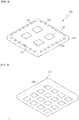
FIGS. 8 to 12 are diagrams for explaining a cavity substrate illustrated inFIG. 3 . -
FIG. 13 is a diagram for explaining the antenna package having the cavity structure according to an exemplary embodiment of the present disclosure. - Hereinafter, the most preferred exemplary embodiments of the present disclosure will be described with reference to the accompanying drawings in order to specifically describe the exemplary embodiments so that those skilled in the art to which the present disclosure pertains may easily implement the technical spirit of the present disclosure. First, in adding reference numerals to the components of each drawing, it should be noted that the same components have the same reference numerals as much as possible even if they are displayed in different drawings. Further, in describing the present disclosure, when it is determined that the detailed description of the related well-known configuration or function may obscure the gist of the present disclosure, the detailed description thereof will be omitted.
- Referring to
FIGS. 1 and2 , an antenna for a 5G network (hereinafter, a 5G antenna) is installed on a base station. The 5G antenna supports communication using an ultra-high frequency by disposing a plurality ofantenna packages 20 in a matrix. - The 5G antenna is configured by mounting the plurality of
antenna packages 20 on amain substrate 10. Themain substrate 10 is made of an organic or organic material such as LTCC and FR4. Themain substrate 10 is formed with a plurality of receiving grooves 12 for receiving theantenna packages 20. The plurality of receiving grooves 12 are disposed in a matrix. Theantenna package 20 is mounted to each of the plurality of receiving grooves 12. As an example, the 5G antenna is formed with 16 receiving grooves 12 disposed in 4 rows and 4 columns, and theantenna package 20 is mounted in each of the receiving grooves 12. - The 5G antenna is manufactured by disposing the
antenna package 20 in the receiving groove 12 and then applying a predetermined pressure to seat theantenna package 20 in the receiving groove 12. - Since the
antenna package 20 has a signal processing element mounted on a surface facing the bottom surface of the receiving groove 12, a separation space is formed between the bottom surface of the receiving groove 12 and theantenna package 20. - The 5G antenna has a problem in that a pressure is applied to the separation space in the process of inserting the
antenna package 20 into the receiving groove 12 to cause deformation, breakage, the depression, distortion, or the like of theantenna package 20, thereby degrading mass productivity, or degrading antenna performance. - Accordingly, an exemplary embodiment of the present disclosure proposes an antenna package having a cavity structure (hereinafter referred to as a cavity antenna package) which prevents the occurrence of deformation and breakage in a process of inserting the antenna package into the receiving groove.
- Referring to
FIG. 3 , acavity antenna package 100 according to an exemplary embodiment of the present disclosure includes anantenna substrate 200 and acavity substrate 300. - The
antenna substrate 200 receives a 5G network frequency band signal (hereinafter, a 5G signal). Theantenna substrate 200 includes a plurality of radiation patterns andsignal processing elements 230. Theantenna substrate 200 processes the 5G signal received through the radiation pattern in thesignal processing element 230 and then transmits the processed 5G signal to themain substrate 10 of the antenna. - Referring to
FIGS. 4 and 5 , theantenna substrate 200 includes aceramic substrate 210, aradiation patch 220, asignal processing element 230, and a first controlsignal transmission electrode 240. Theantenna substrate 200 is inserted into the receiving groove 12 formed in themain substrate 10 of the 5G antenna. The lower surface of theantenna substrate 200 faces the bottom surface of the receiving groove 12. - The
ceramic substrate 210 is a plate-shaped base substrate made of a ceramic material. Theceramic substrate 210 is a low temperature co-fired ceramic (LTCC) base substrate. - As an example, the
ceramic substrate 210 is one of Zirconia Toughened Alumina (ZTA), aluminum nitride (AlN), aluminum oxide (alumina, Al2O3), and silicon nitride (SiN, Si3N4). Theceramic substrate 210 may also be a synthetic ceramic material including one or more of ZTA, aluminum nitride, aluminum oxide, and silicon nitride. - Further, the
ceramic substrate 210 may be modified to be made of a ceramic material having low dielectric constant and dielectric loss for the substrate of the antenna. - The
radiation patch 220 is formed on the upper surface of theceramic substrate 210. Theradiation patch 220 transmits and receives the 5G signal. As an example, theradiation patch 220 is a thin plate made of a conductive material having high electrical conductivity, such as copper, aluminum, gold, or silver. - A plurality of
radiation patches 220 are configured and are disposed in a matrix on the upper surface of theceramic substrate 210. As an example, theradiation patch 220 includes a first radiation patch to a sixteenth radiation patch. - A first radiation patch to a fourth radiation patch form a first row, a fifth radiation patch to an eighth radiation patch form a second row, and a ninth radiation patch to a twelfth radiation patch form a third row, and a thirteenth radiation patch to a sixteenth radiation patch form a fourth row.
- The first radiation patch, the fifth radiation patch, the
ninth radiation patch 220 and the thirteenth radiation patch form a first column, the second radiation patch, the sixth radiation patch, thetenth radiation patch 220, and the fourteenth radiation patch form a second column, the third radiation patch, the seventh radiation patch, theeleventh radiation patch 220, and the fifteenth radiation patch form a third column, the fourth radiation patch, the eighth radiation patch, thetwelfth radiation patch 220, and the sixteenth radiation patch form a fourth column. Accordingly, the first to sixteenth radiation patches form a matrix of 4X4 arrangement on the upper surface of theceramic substrate 210. - The
signal processing element 230 is formed on the lower surface of theceramic substrate 210. A plurality ofsignal processing elements 230 are configured and are disposed in a matrix on the lower surface of theceramic substrate 210. Thesignal processing element 230 signal-processes the 5G signal received from the plurality ofradiation patches 220. Thesignal processing element 230 transmits the 5G signal through theradiation patch 220. - As an example, the
signal processing element 230 includes a first signal processing element to a fourth signal processing element. The first signal processing element is disposed close to a first side surface and a second side surface of theceramic substrate 210, the second signal processing element is disposed close to the second side surface and a third side surface thereof, the third signal processing element is disposed close to the first side surface and the fourth side surface of theceramic substrate 210, and the fourth signal processing element is disposed close to the third side surface and the fourth side surface thereof. Accordingly, the first signal processing element to the fourth signal processing element form a matrix of 2X2 arrangement. - The
signal processing element 230 is connected to the plurality ofradiation patches 220. Thesignal processing element 230 feeds the plurality ofradiation patches 220 through a feed line (not illustrated) formed inside theceramic substrate 210. - As an example, the first signal processing element is connected to the first radiation pattern, the second radiation pattern, the fifth radiation pattern, and the sixth radiation pattern. The second signal processing element is connected to the third radiation pattern, the fourth radiation pattern, the seventh radiation pattern, and the eighth radiation pattern. The third signal processing element is connected to the ninth radiation pattern, the tenth radiation pattern, the thirteenth radiation pattern, and the fourteenth radiation pattern. The fourth signal processing element is connected to the eleventh radiation pattern, the twelfth radiation pattern, the fifteenth radiation pattern, and the sixteenth radiation pattern. Accordingly, the
signal processing element 230 is connected to four radiation patterns. - The
signal processing element 230 may be connected to a feeding pattern (not illustrated) formed inside theceramic substrate 210. The feeding pattern is connected to thesignal processing element 230 through a feeding line. Thesignal processing element 230 supplies a signal for wireless signal transmission in the feeding pattern. The feeding pattern may feed theradiation patch 220 through coupling. Here, the coupling means that the feeding pattern and the radiation pattern are not directly in contact with each other but are electrically connected in a separated state. - The first control
signal transmission electrode 240 is formed on the lower surface of theceramic substrate 210. A plurality of first controlsignal transmission electrodes 240 are configured and are disposed to be spaced apart from each other. The first controlsignal transmission electrode 240 is located between the outer circumstance of the ceramicsignal processing element 230 and the outer circumstance of theceramic substrate 210. - The first control
signal transmission electrode 240 is connected to thesignal processing element 230 through an electrode (not illustrated) formed inside theceramic substrate 210. The plurality of first controlsignal transmission electrodes 240 are connected to onesignal processing element 230. The first controlsignal transmission electrode 240 transmits the signal processing element control signal transmitted from themain substrate 10 of the 5G antenna to thesignal processing element 230. - Referring to
FIG. 6 , theantenna substrate 200 may further include a first RFsignal transmission pattern 250 and anRF signal distributor 260. - The first RF
signal transmission pattern 250 is formed on the lower surface of or inside theceramic substrate 210. One end of the first RFsignal transmission pattern 250 is located on one side of theceramic substrate 210. One end of the first RFsignal transmission pattern 250 is connected to the RFsignal transmission electrode 340 formed on thecavity substrate 300 through a via hole formed in thecavity substrate 300. The other end of the first RFsignal transmission pattern 250 is connected to the input terminal of theRF signal distributor 260. - The
RF signal distributor 260 is composed of a distributor having one input terminal and a plurality of output terminals. The input terminal is connected to the first RFsignal transmission pattern 250. The plurality of output terminals are connected to have one-to-one correspondence with the plurality ofsignal processing elements 230. - The
RF signal distributor 260 is formed at the center of the lower surface of theceramic substrate 210. As an example, theRF signal distributor 260 is disposed in a separation space between the first signal processing element to the fourth signal processing element. - The
RF signal distributor 260 may also be formed inside theceramic substrate 210. At this time, the plurality of output terminals are connected to thesignal processing element 230 through the via hole. - The
RF signal distributor 260 branches the 5G signal to transmit the branched 5G signal to the first signal processing element to the fourth signal processing element. TheRF signal distributor 260 transmits to themain substrate 10 the 5G frequency band signal (that is, the signal received from the radiation patch 220) signal-processed by the first signal processing element to the fourth signal processing element. - As an example, the
RF signal distributor 260 is a 4-Way Wilkinson distributor. The 4-Way Wilkinson distributor is composed of four output terminals. The first to fourth signal processing elements are each connected to the four output terminals. - Referring to
FIG. 7 , theantenna substrate 200 may further include a firstRF signal distributor 262, a secondRF signal distributor 264, and a first RFsignal transmission pattern 250. - The first
RF signal distributor 262 and the secondRF signal distributor 264 are formed on the lower surface of or inside theceramic substrate 210. The firstRF signal distributor 262 is disposed in a separation space between the first signal processing element and the third signal processing element. - The first
RF signal distributor 262 is composed of a distributor having one input terminal and a pair of output terminals. The input terminal is connected to one end of the first RFsignal transmission pattern 250. The pair of output terminals are each connected to have one-to-one correspondence with thesignal processing element 230. - As an example, the first
RF signal distributor 262 is a 2-Way Wilkinson distributor having two output terminals. The input terminal of the 2-Way Wilkinson distributor is connected to one end of the first RFsignal transmission pattern 250. The first output terminal of the 2-Way Wilkinson distributor is connected to the first signal processing element, and the second output terminal is connected to the third signal processing element. - The second
RF signal distributor 264 and the secondRF signal distributor 264 are formed on the lower surface of or inside theceramic substrate 210. The secondRF signal distributor 264 is disposed in a separation space between the second signal processing element and the fourth signal processing element. - The second
RF signal distributor 264 is composed of a distributor having one input terminal and a pair of output terminals. The input terminal is connected to the other end of the first RFsignal transmission pattern 250. The pair of output terminals are each connected to have one-to-one correspondence with thesignal processing element 230. - As an example, the second
RF signal distributor 264 is a 2-Way Wilkinson distributor having two output terminals. The input terminal of the 2-Way Wilkinson distributor is connected to the other end of the first RFsignal transmission pattern 250. The first output terminal of the 2-Way Wilkinson distributor is connected to the second signal processing element, and the second output terminal thereof is connected to the fourth signal processing element. - The first RF
signal transmission pattern 250 is formed on the lower surface of or inside theceramic substrate 210. One end of the first RFsignal transmission pattern 250 is connected to the input terminal of the firstRF signal distributor 262. The other end of the first RFsignal transmission pattern 250 is connected to the input terminal of the secondRF signal distributor 264. The first RFsignal transmission pattern 250 is connected to the second RFsignal transmission pattern 350 formed on thecavity substrate 300 through a via hole formed in thecavity substrate 300. - The
antenna package 100 having the cavity structure according to an exemplary embodiment of the present disclosure may branch the RF signal using the 2-Way Wilkinson distributor, thereby minimizing dielectric loss. - The
cavity substrate 300 is located on the lower surface of theantenna substrate 200. Thecavity substrate 300 is a reinforcing member for preventing deformation and breakage due to pressure applied when thecavity antenna package 100 is inserted into and mounted in the receiving groove 12 of themain substrate 10. - The
cavity substrate 300 is integrally formed with theantenna substrate 200. Thecavity substrate 300 is made of the same ceramic material as theantenna substrate 200, and is simultaneously formed with theantenna substrate 200 through the LTCC process. - The
cavity substrate 300 may be manufactured while being separated from theantenna substrate 200 and then bonded to the lower surface of theantenna substrate 200. Thecavity substrate 300 may be made of the same ceramic material as theantenna substrate 200. Thecavity substrate 300 may be made of a material different from that of the antenna substrate 200 (for example, FR4 or the like) to reduce manufacturing cost and improve mass productivity. - The thickness of the
cavity substrate 300 is preferably the thickness or more of thesignal processing element 230 exposed to the lower surface of theantenna substrate 200. This is to prevent deformation and breakage of thecavity antenna package 100 by preventing the occurrence of the separation space when thecavity antenna package 100 is inserted into themain substrate 10. - Referring to
FIGS. 8 and 9 , thecavity substrate 300 includes acavity frame 310. - The
cavity frame 310 has a rectangular plate-shaped frame. Thecavity frame 310 is formed with anaccommodation portion 320 which accommodates thesignal processing element 230 formed on the lower surface of theantenna substrate 200. Theaccommodation portion 320 is formed in a rectangular hole shape with the upper and lower ends open to accommodate all of thesignal processing elements 230 formed on the lower surface of theantenna substrate 200. Accordingly, thecavity frame 310 is formed in a square frame shape. - A second control
signal transmission electrode 330 is formed on the lower surface of thecavity frame 310. The second controlsignal transmission electrode 330 is disposed close to the outer circumstance of thecavity frame 310. A plurality of second controlsignal transmission electrodes 330 are configured and are formed to be spaced apart from each other on the lower surface of thecavity frame 310. The second controlsignal transmission electrode 330 is connected to have one-to-one correspondence with the first controlsignal transmission electrode 240 formed on theantenna substrate 200 through a via hole penetrating thecavity frame 310. - The RF
signal transmission electrode 340 is formed on the lower surface of thecavity frame 310. The RFsignal transmission electrode 340 is formed to be spaced apart from the second controlsignal transmission electrode 330. The RFsignal transmission electrode 340 is connected to the first RF signal transmission pattern 250 (seeFIG. 6 ) of theantenna substrate 200 through the via hole. Accordingly, thecavity antenna package 100 forms a 4-Way Wilkinson distributor. - Referring to
FIG. 10 , a plurality ofaccommodation portions 320 may be formed in thecavity frame 310. - The plurality of
accommodation portions 320 each accommodates onesignal processing element 230. As an example, thecavity substrate 300 includes thecavity frame 310 having a lattice structure in which a first accommodation portion to a fourth accommodation portion are formed. The plurality ofaccommodation portions 320 are formed in a square hole shape with the upper and lower ends open. Accordingly, thecavity frame 310 is formed in a lattice structure. - As an example, the
cavity frame 310 forms a configuration in which four accommodation portions 320 (that is, the first accommodation portion to the fourth accommodation portion) are disposed in a lattice shape by combining a transverse diaphragm and a longitudinal diaphragm. Thecavity frame 310 is connected in a direction in which the transverse diaphragm and the longitudinal diaphragm are perpendicular to each other to form a square frame shape as a whole, and at the same time, each of theaccommodation portions 320 is formed in a rectangular hole shape. The first signal processing element is accommodated in the first accommodation portion, the second signal processing element is accommodated in the second accommodation portion, the third signal processing element is accommodated in the third accommodation portion, and the fourth signal processing element is accommodated in the fourth accommodation portion. - As described above, the
cavity substrate 300 may be formed with the plurality ofaccommodation portions 320 to form thecavity frame 310 having the lattice structure, thereby increasing the reinforcing strength of the antenna package. - Referring to
FIGS. 11 and12 , a second RFsignal transmission pattern 350 may be formed on the lower surface of thecavity frame 310. One end of the second RFsignal transmission pattern 350 is connected to the RFsignal transmission electrode 340. The other end of the second RFsignal transmission pattern 350 is formed to extend toward the center of thecavity frame 310 and is connected to the first RF signal transmission pattern 250 (seeFIG. 7 ) of theantenna substrate 200 through a via hole. - Accordingly, the first RF
signal transmission pattern 250 and the second RFsignal transmission pattern 350 form a T junction distributor. - The
cavity antenna package 100 may form the 2-Way Wilkinson distributor and the T junction distributor to distribute signals, thereby minimizing dielectric loss compared to the structure in which the 4-Way Wilkinson distributor is formed. - Referring to
FIG. 13 , thecavity antenna package 100 may form thecavity substrate 300 on theantenna substrate 200, thereby preventing deformation and breakage of the antenna package in a process in which thecavity substrate 300 supports the separation space between theantenna substrate 200 and the bottom surface of the receiving groove 12 to insert the antenna package into the receiving groove 12 of themain substrate 10. - Although the preferred exemplary embodiment of the present disclosure has been described above, it is understood that the present disclosure may be modified in various forms, and those skilled in the art may carry out various modified examples and changed examples without departing from the scope of the claims of the present disclosure.
Claims (16)
- An antenna package having a cavity structure comprising:an antenna substrate which has a plurality of radiation patches formed on the upper surface thereof, and a plurality of signal processing elements formed on the lower surface thereof; anda cavity substrate which is formed with accommodation portions accommodating the plurality of signal processing elements, and disposed on the lower surface of the antenna substrate.
- The antenna package having the cavity structure of claim 1,
wherein the antenna substrate comprises:a plate-shaped ceramic substrate; anda plurality of first control signal transmission electrodes which are formed on the lower surface of the ceramic substrate, and disposed to be spaced apart from each other along the outer circumference of the ceramic substrate, andwherein the plurality of radiation patches are disposed in a matrix on the upper surface of the ceramic substrate, andwherein the plurality of signal processing elements are disposed in a matrix on the lower surface of the ceramic substrate. - The antenna package having the cavity structure of claim 2,
wherein the antenna substrate further comprises: a first RF signal transmission pattern formed on the ceramic substrate, and
wherein one end of the first RF signal transmission pattern is connected to an RF signal transmission electrode of the cavity substrate through a via hole. - The antenna package having the cavity structure of claim 3,
wherein the antenna substrate further comprises:an RF signal distributor having an input terminal and a plurality of output terminals, and formed on the ceramic substrate, andwherein the input terminal is connected to the other end of the first RF signal transmission pattern, and the plurality of output terminals are connected to have one-to-one correspondence with the plurality of signal processing elements. - The antenna package having the cavity structure of claim 4,
wherein the RF signal distributor is a 4-Way Wilkinson distributor. - The antenna package having the cavity structure of claim 2,
wherein the antenna substrate further comprises:a first RF signal transmission pattern which is formed on the ceramic substrate;a first RF signal distributor which is formed on the ceramic substrate, and has an input terminal connected to one end of the first RF signal transmission pattern and a plurality of output terminals connected to some of the plurality of signal processing elements, anda second RF signal distributor which is formed on the ceramic substrate to be spaced apart from the first RF signal distributor, and has an input terminal connected to the other end of the first RF signal transmission pattern and a plurality of output terminals connected to the plurality of signal processing elements other than some of the plurality of signal processing elements. - The antenna package having the cavity structure of claim 6,
wherein the first RF signal distributor and the second RF signal distributor are 2-Way Wilkinson distributors. - The antenna package having the cavity structure of claim 1,
wherein the cavity substrate comprises: a cavity frame in which the accommodation portion is formed. - The antenna package having the cavity structure of claim 8,
wherein the cavity frame has a rectangular frame shape in which one accommodation portion is formed. - The antenna package having the cavity structure of claim 8,
wherein the cavity substrate further comprises: a second control signal transmission electrode which is formed on the lower surface of the cavity frame, and connected to the first control signal transmission electrode formed on the antenna substrate. - The antenna package having the cavity structure of claim 10, further comprising:an RF signal transmission electrode which is formed on the lower surface of the cavity frame to be spaced apart from the second control signal transmission electrode,wherein the RF signal transmission electrode is connected to the first RF signal transmission pattern of the antenna substrate.
- The antenna package having the cavity structure of claim 8,
wherein the cavity frame has a lattice shape in which a plurality of accommodation portions are disposed in a matrix. - The antenna package having the cavity structure of claim 12,
wherein the cavity substrate further comprises a second RF signal transmission pattern which is formed on the lower surface of the cavity frame, and
wherein one end of the second RF signal transmission pattern is connected to an RF signal transmission electrode, and the other end of the second RF signal transmission pattern is formed to extend toward the center of the cavity frame. - The antenna package having the cavity structure of claim 13,
wherein the other end of the second RF signal transmission pattern is connected to a first RF signal transmission pattern of the antenna substrate through a via hole. - The antenna package having the cavity structure of claim 1,
wherein the cavity substrate is made of the same ceramic material as the antenna substrate. - The antenna package having the cavity structure of claim 1,
wherein the cavity substrate is made of a material different from that of the antenna substrate.
Applications Claiming Priority (1)
| Application Number | Priority Date | Filing Date | Title |
|---|---|---|---|
| PCT/KR2018/012334 WO2020080575A1 (en) | 2018-10-18 | 2018-10-18 | Antenna package having cavity structure |
Publications (4)
| Publication Number | Publication Date |
|---|---|
| EP3734764A1 true EP3734764A1 (en) | 2020-11-04 |
| EP3734764A4 EP3734764A4 (en) | 2021-08-11 |
| EP3734764B1 EP3734764B1 (en) | 2023-11-08 |
| EP3734764C0 EP3734764C0 (en) | 2023-11-08 |
Family
ID=70282928
Family Applications (1)
| Application Number | Title | Priority Date | Filing Date |
|---|---|---|---|
| EP18937300.4A Active EP3734764B1 (en) | 2018-10-18 | 2018-10-18 | Antenna package having cavity structure |
Country Status (5)
| Country | Link |
|---|---|
| US (1) | US11329396B2 (en) |
| EP (1) | EP3734764B1 (en) |
| JP (1) | JP6987999B2 (en) |
| CN (1) | CN111566876B (en) |
| WO (1) | WO2020080575A1 (en) |
Families Citing this family (2)
| Publication number | Priority date | Publication date | Assignee | Title |
|---|---|---|---|---|
| US10804188B2 (en) * | 2018-09-07 | 2020-10-13 | Intel Corporation | Electronic device including a lateral trace |
| CN114745018B (en) * | 2022-03-17 | 2024-05-28 | 南京瑞基通讯技术有限公司 | Radio frequency front end component adopting high-performance ceramic material |
Family Cites Families (22)
| Publication number | Priority date | Publication date | Assignee | Title |
|---|---|---|---|---|
| JP2004327641A (en) * | 2003-04-24 | 2004-11-18 | Tdk Corp | Electronic component module |
| JP2005086603A (en) * | 2003-09-10 | 2005-03-31 | Tdk Corp | Electronic component module and manufacturing method thereof |
| JP4684730B2 (en) * | 2004-04-30 | 2011-05-18 | シャープ株式会社 | High frequency semiconductor device, transmission device, and reception device |
| US7183622B2 (en) * | 2004-06-30 | 2007-02-27 | Intel Corporation | Module integrating MEMS and passive components |
| US7675466B2 (en) * | 2007-07-02 | 2010-03-09 | International Business Machines Corporation | Antenna array feed line structures for millimeter wave applications |
| KR100892235B1 (en) | 2007-08-28 | 2009-04-09 | 주식회사 이엠따블유안테나 | Quadruple polarization antenna and feed circuit for him |
| US7692590B2 (en) * | 2008-02-20 | 2010-04-06 | International Business Machines Corporation | Radio frequency (RF) integrated circuit (IC) packages with integrated aperture-coupled patch antenna(s) |
| CN201378625Y (en) * | 2009-03-26 | 2010-01-06 | 北京华大智宝电子系统有限公司 | Flat plane antenna with novel cavity gap structure |
| US8901688B2 (en) * | 2011-05-05 | 2014-12-02 | Intel Corporation | High performance glass-based 60 ghz / mm-wave phased array antennas and methods of making same |
| KR101208241B1 (en) * | 2011-07-12 | 2012-12-04 | 삼성전기주식회사 | Semiconductor package |
| US9153542B2 (en) * | 2012-08-01 | 2015-10-06 | Advanced Semiconductor Engineering, Inc. | Semiconductor package having an antenna and manufacturing method thereof |
| WO2014020787A1 (en) | 2012-08-03 | 2014-02-06 | パナソニック株式会社 | Electronic component module and mounting body therefor |
| JP6347424B2 (en) | 2013-06-25 | 2018-06-27 | パナソニックIpマネジメント株式会社 | Wireless module |
| JP6402962B2 (en) * | 2013-07-17 | 2018-10-10 | パナソニックIpマネジメント株式会社 | High frequency module |
| US9659904B2 (en) * | 2013-12-12 | 2017-05-23 | Intel Corporation | Distributed on-package millimeter-wave radio |
| US10074910B1 (en) * | 2014-08-01 | 2018-09-11 | Rockwell Collins, Inc. | Switchable X band communication panel |
| CN107078405B (en) * | 2014-10-20 | 2021-03-05 | 株式会社村田制作所 | Wireless communication module |
| KR102117473B1 (en) * | 2015-03-18 | 2020-06-01 | 삼성전기주식회사 | Mounting module, antenna apparatus and method for manufacturing mounting module |
| CN205029022U (en) * | 2015-09-29 | 2016-02-10 | 中国电子科技集团公司第五十四研究所 | Portable circular polarization microstrip antenna array row |
| WO2019008913A1 (en) * | 2017-07-06 | 2019-01-10 | 株式会社村田製作所 | ANTENNA MODULE |
| KR102323005B1 (en) * | 2017-10-17 | 2021-11-09 | 주식회사 아모텍 | Antenna package having cavity structure |
| CN108306118B (en) * | 2018-01-30 | 2020-04-28 | 中国电子科技集团公司第三十八研究所 | Extensible plate type active array antenna |
-
2018
- 2018-10-18 EP EP18937300.4A patent/EP3734764B1/en active Active
- 2018-10-18 US US16/959,103 patent/US11329396B2/en active Active
- 2018-10-18 JP JP2020536753A patent/JP6987999B2/en active Active
- 2018-10-18 WO PCT/KR2018/012334 patent/WO2020080575A1/en not_active Ceased
- 2018-10-18 CN CN201880084932.5A patent/CN111566876B/en active Active
Also Published As
| Publication number | Publication date |
|---|---|
| JP6987999B2 (en) | 2022-01-05 |
| JP2021509560A (en) | 2021-03-25 |
| WO2020080575A1 (en) | 2020-04-23 |
| EP3734764A4 (en) | 2021-08-11 |
| EP3734764B1 (en) | 2023-11-08 |
| US11329396B2 (en) | 2022-05-10 |
| EP3734764C0 (en) | 2023-11-08 |
| CN111566876A (en) | 2020-08-21 |
| US20200335877A1 (en) | 2020-10-22 |
| CN111566876B (en) | 2021-07-30 |
Similar Documents
| Publication | Publication Date | Title |
|---|---|---|
| KR102323005B1 (en) | Antenna package having cavity structure | |
| US11251538B2 (en) | Antenna module | |
| CN106537682B (en) | Waveguide and transmission line in the gap between parallel conducting planes | |
| US6876328B2 (en) | Multiple-resonant antenna, antenna module, and radio device using the multiple-resonant antenna | |
| CN104685708B (en) | Wireless communication node with antenna arrangement for dual-band reception and transmission | |
| EP3535806B1 (en) | Dual-band antenna element and base station | |
| JPH11355033A (en) | Antenna device | |
| CN113067587B (en) | RF components and communication equipment | |
| US11329396B2 (en) | Antenna package having cavity structure | |
| CN112771725B (en) | Antenna module, communication device and array antenna | |
| EP3809519A1 (en) | Cavity filter and connecting structure included therein | |
| FR3105613B1 (en) | Elementary cell of a transmitting network | |
| CN108508392A (en) | A kind of four beam type Electronic Calibration part of T-type switch | |
| KR20200092615A (en) | Antenna in package module | |
| US20200412008A1 (en) | Antenna device and low-profile antenna | |
| US20250062545A1 (en) | Antenna with dual polarized radiators | |
| CN107425280B (en) | A millimeter-wave flat-panel phased array antenna architecture | |
| US20210336355A1 (en) | Co-located antennas with coupled arms | |
| US20200052378A1 (en) | Antenna system and mobile terminal | |
| CN212062693U (en) | Antenna system and electronic device using antenna system | |
| JP2001127529A (en) | Antenna-integrated duplexer board | |
| US20250337149A1 (en) | Multi-input and multi-output antenna apparatus | |
| JP2023526582A (en) | Antenna arrangements for mobile radio systems, stacked antenna systems and mobile radio antennas comprising antenna arrangements and stacked antenna systems | |
| JP2001267840A (en) | Antenna-integrated duplexer board | |
| US10164329B2 (en) | Wideband MIMO array with low passive intermodulation attributes |
Legal Events
| Date | Code | Title | Description |
|---|---|---|---|
| STAA | Information on the status of an ep patent application or granted ep patent |
Free format text: STATUS: THE INTERNATIONAL PUBLICATION HAS BEEN MADE |
|
| PUAI | Public reference made under article 153(3) epc to a published international application that has entered the european phase |
Free format text: ORIGINAL CODE: 0009012 |
|
| STAA | Information on the status of an ep patent application or granted ep patent |
Free format text: STATUS: REQUEST FOR EXAMINATION WAS MADE |
|
| 17P | Request for examination filed |
Effective date: 20200623 |
|
| AK | Designated contracting states |
Kind code of ref document: A1 Designated state(s): AL AT BE BG CH CY CZ DE DK EE ES FI FR GB GR HR HU IE IS IT LI LT LU LV MC MK MT NL NO PL PT RO RS SE SI SK SM TR |
|
| AX | Request for extension of the european patent |
Extension state: BA ME |
|
| A4 | Supplementary search report drawn up and despatched |
Effective date: 20210712 |
|
| RIC1 | Information provided on ipc code assigned before grant |
Ipc: H01Q 21/06 20060101AFI20210706BHEP Ipc: H01Q 1/38 20060101ALI20210706BHEP Ipc: H01Q 1/22 20060101ALI20210706BHEP Ipc: H01Q 1/20 20060101ALI20210706BHEP Ipc: H01Q 21/00 20060101ALI20210706BHEP |
|
| DAV | Request for validation of the european patent (deleted) | ||
| DAX | Request for extension of the european patent (deleted) | ||
| GRAP | Despatch of communication of intention to grant a patent |
Free format text: ORIGINAL CODE: EPIDOSNIGR1 |
|
| STAA | Information on the status of an ep patent application or granted ep patent |
Free format text: STATUS: GRANT OF PATENT IS INTENDED |
|
| INTG | Intention to grant announced |
Effective date: 20230512 |
|
| GRAS | Grant fee paid |
Free format text: ORIGINAL CODE: EPIDOSNIGR3 |
|
| GRAA | (expected) grant |
Free format text: ORIGINAL CODE: 0009210 |
|
| STAA | Information on the status of an ep patent application or granted ep patent |
Free format text: STATUS: THE PATENT HAS BEEN GRANTED |
|
| AK | Designated contracting states |
Kind code of ref document: B1 Designated state(s): AL AT BE BG CH CY CZ DE DK EE ES FI FR GB GR HR HU IE IS IT LI LT LU LV MC MK MT NL NO PL PT RO RS SE SI SK SM TR |
|
| REG | Reference to a national code |
Ref country code: GB Ref legal event code: FG4D |
|
| REG | Reference to a national code |
Ref country code: CH Ref legal event code: EP |
|
| REG | Reference to a national code |
Ref country code: DE Ref legal event code: R096 Ref document number: 602018061018 Country of ref document: DE |
|
| REG | Reference to a national code |
Ref country code: IE Ref legal event code: FG4D |
|
| U01 | Request for unitary effect filed |
Effective date: 20231204 |
|
| U07 | Unitary effect registered |
Designated state(s): AT BE BG DE DK EE FI FR IT LT LU LV MT NL PT SE SI Effective date: 20231208 |
|
| PG25 | Lapsed in a contracting state [announced via postgrant information from national office to epo] |
Ref country code: GR Free format text: LAPSE BECAUSE OF FAILURE TO SUBMIT A TRANSLATION OF THE DESCRIPTION OR TO PAY THE FEE WITHIN THE PRESCRIBED TIME-LIMIT Effective date: 20240209 |
|
| PG25 | Lapsed in a contracting state [announced via postgrant information from national office to epo] |
Ref country code: IS Free format text: LAPSE BECAUSE OF FAILURE TO SUBMIT A TRANSLATION OF THE DESCRIPTION OR TO PAY THE FEE WITHIN THE PRESCRIBED TIME-LIMIT Effective date: 20240308 |
|
| PG25 | Lapsed in a contracting state [announced via postgrant information from national office to epo] |
Ref country code: ES Free format text: LAPSE BECAUSE OF FAILURE TO SUBMIT A TRANSLATION OF THE DESCRIPTION OR TO PAY THE FEE WITHIN THE PRESCRIBED TIME-LIMIT Effective date: 20231108 |
|
| PG25 | Lapsed in a contracting state [announced via postgrant information from national office to epo] |
Ref country code: IS Free format text: LAPSE BECAUSE OF FAILURE TO SUBMIT A TRANSLATION OF THE DESCRIPTION OR TO PAY THE FEE WITHIN THE PRESCRIBED TIME-LIMIT Effective date: 20240308 Ref country code: GR Free format text: LAPSE BECAUSE OF FAILURE TO SUBMIT A TRANSLATION OF THE DESCRIPTION OR TO PAY THE FEE WITHIN THE PRESCRIBED TIME-LIMIT Effective date: 20240209 Ref country code: ES Free format text: LAPSE BECAUSE OF FAILURE TO SUBMIT A TRANSLATION OF THE DESCRIPTION OR TO PAY THE FEE WITHIN THE PRESCRIBED TIME-LIMIT Effective date: 20231108 |
|
| PG25 | Lapsed in a contracting state [announced via postgrant information from national office to epo] |
Ref country code: RS Free format text: LAPSE BECAUSE OF FAILURE TO SUBMIT A TRANSLATION OF THE DESCRIPTION OR TO PAY THE FEE WITHIN THE PRESCRIBED TIME-LIMIT Effective date: 20231108 Ref country code: PL Free format text: LAPSE BECAUSE OF FAILURE TO SUBMIT A TRANSLATION OF THE DESCRIPTION OR TO PAY THE FEE WITHIN THE PRESCRIBED TIME-LIMIT Effective date: 20231108 Ref country code: NO Free format text: LAPSE BECAUSE OF FAILURE TO SUBMIT A TRANSLATION OF THE DESCRIPTION OR TO PAY THE FEE WITHIN THE PRESCRIBED TIME-LIMIT Effective date: 20240208 Ref country code: HR Free format text: LAPSE BECAUSE OF FAILURE TO SUBMIT A TRANSLATION OF THE DESCRIPTION OR TO PAY THE FEE WITHIN THE PRESCRIBED TIME-LIMIT Effective date: 20231108 |
|
| PG25 | Lapsed in a contracting state [announced via postgrant information from national office to epo] |
Ref country code: CZ Free format text: LAPSE BECAUSE OF FAILURE TO SUBMIT A TRANSLATION OF THE DESCRIPTION OR TO PAY THE FEE WITHIN THE PRESCRIBED TIME-LIMIT Effective date: 20231108 |
|
| PG25 | Lapsed in a contracting state [announced via postgrant information from national office to epo] |
Ref country code: SK Free format text: LAPSE BECAUSE OF FAILURE TO SUBMIT A TRANSLATION OF THE DESCRIPTION OR TO PAY THE FEE WITHIN THE PRESCRIBED TIME-LIMIT Effective date: 20231108 |
|
| PG25 | Lapsed in a contracting state [announced via postgrant information from national office to epo] |
Ref country code: SM Free format text: LAPSE BECAUSE OF FAILURE TO SUBMIT A TRANSLATION OF THE DESCRIPTION OR TO PAY THE FEE WITHIN THE PRESCRIBED TIME-LIMIT Effective date: 20231108 Ref country code: SK Free format text: LAPSE BECAUSE OF FAILURE TO SUBMIT A TRANSLATION OF THE DESCRIPTION OR TO PAY THE FEE WITHIN THE PRESCRIBED TIME-LIMIT Effective date: 20231108 Ref country code: RO Free format text: LAPSE BECAUSE OF FAILURE TO SUBMIT A TRANSLATION OF THE DESCRIPTION OR TO PAY THE FEE WITHIN THE PRESCRIBED TIME-LIMIT Effective date: 20231108 Ref country code: CZ Free format text: LAPSE BECAUSE OF FAILURE TO SUBMIT A TRANSLATION OF THE DESCRIPTION OR TO PAY THE FEE WITHIN THE PRESCRIBED TIME-LIMIT Effective date: 20231108 |
|
| REG | Reference to a national code |
Ref country code: DE Ref legal event code: R097 Ref document number: 602018061018 Country of ref document: DE |
|
| PLBE | No opposition filed within time limit |
Free format text: ORIGINAL CODE: 0009261 |
|
| STAA | Information on the status of an ep patent application or granted ep patent |
Free format text: STATUS: NO OPPOSITION FILED WITHIN TIME LIMIT |
|
| 26N | No opposition filed |
Effective date: 20240809 |
|
| U20 | Renewal fee for the european patent with unitary effect paid |
Year of fee payment: 7 Effective date: 20241024 |
|
| REG | Reference to a national code |
Ref country code: CH Ref legal event code: PL |
|
| PG25 | Lapsed in a contracting state [announced via postgrant information from national office to epo] |
Ref country code: MC Free format text: LAPSE BECAUSE OF FAILURE TO SUBMIT A TRANSLATION OF THE DESCRIPTION OR TO PAY THE FEE WITHIN THE PRESCRIBED TIME-LIMIT Effective date: 20231108 |
|
| PG25 | Lapsed in a contracting state [announced via postgrant information from national office to epo] |
Ref country code: CH Free format text: LAPSE BECAUSE OF NON-PAYMENT OF DUE FEES Effective date: 20241031 |
|
| PGFP | Annual fee paid to national office [announced via postgrant information from national office to epo] |
Ref country code: GB Payment date: 20250922 Year of fee payment: 8 |
|
| PG25 | Lapsed in a contracting state [announced via postgrant information from national office to epo] |
Ref country code: IE Free format text: LAPSE BECAUSE OF NON-PAYMENT OF DUE FEES Effective date: 20241018 |
|
| U20 | Renewal fee for the european patent with unitary effect paid |
Year of fee payment: 8 Effective date: 20251022 |
|
| PG25 | Lapsed in a contracting state [announced via postgrant information from national office to epo] |
Ref country code: CY Free format text: LAPSE BECAUSE OF FAILURE TO SUBMIT A TRANSLATION OF THE DESCRIPTION OR TO PAY THE FEE WITHIN THE PRESCRIBED TIME-LIMIT; INVALID AB INITIO Effective date: 20181018 |
|
| PG25 | Lapsed in a contracting state [announced via postgrant information from national office to epo] |
Ref country code: HU Free format text: LAPSE BECAUSE OF FAILURE TO SUBMIT A TRANSLATION OF THE DESCRIPTION OR TO PAY THE FEE WITHIN THE PRESCRIBED TIME-LIMIT; INVALID AB INITIO Effective date: 20181018 |