EP3734761B1 - Loop type antenna and electronic device including same - Google Patents
Loop type antenna and electronic device including same Download PDFInfo
- Publication number
- EP3734761B1 EP3734761B1 EP19744449.0A EP19744449A EP3734761B1 EP 3734761 B1 EP3734761 B1 EP 3734761B1 EP 19744449 A EP19744449 A EP 19744449A EP 3734761 B1 EP3734761 B1 EP 3734761B1
- Authority
- EP
- European Patent Office
- Prior art keywords
- conductive pattern
- conductive
- electronic device
- disposed
- plane
- Prior art date
- Legal status (The legal status is an assumption and is not a legal conclusion. Google has not performed a legal analysis and makes no representation as to the accuracy of the status listed.)
- Active
Links
- 238000004891 communication Methods 0.000 claims description 283
- 230000005855 radiation Effects 0.000 claims description 54
- 239000010410 layer Substances 0.000 description 71
- 239000000470 constituent Substances 0.000 description 12
- 230000006870 function Effects 0.000 description 10
- 238000012545 processing Methods 0.000 description 9
- 239000000758 substrate Substances 0.000 description 8
- 229910052751 metal Inorganic materials 0.000 description 6
- 239000002184 metal Substances 0.000 description 6
- 238000010586 diagram Methods 0.000 description 5
- 238000005516 engineering process Methods 0.000 description 5
- 238000004590 computer program Methods 0.000 description 4
- 101001045744 Sus scrofa Hepatocyte nuclear factor 1-beta Proteins 0.000 description 3
- 230000015556 catabolic process Effects 0.000 description 3
- 238000006731 degradation reaction Methods 0.000 description 3
- 239000007769 metal material Substances 0.000 description 3
- 239000003973 paint Substances 0.000 description 3
- 230000000704 physical effect Effects 0.000 description 3
- 238000007747 plating Methods 0.000 description 3
- 229920000642 polymer Polymers 0.000 description 3
- 230000001133 acceleration Effects 0.000 description 2
- 229910052782 aluminium Inorganic materials 0.000 description 2
- XAGFODPZIPBFFR-UHFFFAOYSA-N aluminium Chemical compound [Al] XAGFODPZIPBFFR-UHFFFAOYSA-N 0.000 description 2
- 230000005540 biological transmission Effects 0.000 description 2
- 239000004020 conductor Substances 0.000 description 2
- 230000000694 effects Effects 0.000 description 2
- 239000000446 fuel Substances 0.000 description 2
- 239000011521 glass Substances 0.000 description 2
- 230000007774 longterm Effects 0.000 description 2
- 239000000463 material Substances 0.000 description 2
- 230000005404 monopole Effects 0.000 description 2
- 230000001105 regulatory effect Effects 0.000 description 2
- 230000035807 sensation Effects 0.000 description 2
- 238000004088 simulation Methods 0.000 description 2
- 230000005236 sound signal Effects 0.000 description 2
- 229910001220 stainless steel Inorganic materials 0.000 description 2
- 239000010935 stainless steel Substances 0.000 description 2
- FYYHWMGAXLPEAU-UHFFFAOYSA-N Magnesium Chemical compound [Mg] FYYHWMGAXLPEAU-UHFFFAOYSA-N 0.000 description 1
- 230000002146 bilateral effect Effects 0.000 description 1
- 230000010267 cellular communication Effects 0.000 description 1
- 230000001413 cellular effect Effects 0.000 description 1
- 239000000919 ceramic Substances 0.000 description 1
- 238000006243 chemical reaction Methods 0.000 description 1
- 239000011247 coating layer Substances 0.000 description 1
- 238000011161 development Methods 0.000 description 1
- 239000003989 dielectric material Substances 0.000 description 1
- 230000007613 environmental effect Effects 0.000 description 1
- 230000001939 inductive effect Effects 0.000 description 1
- 230000010354 integration Effects 0.000 description 1
- 230000003155 kinesthetic effect Effects 0.000 description 1
- 229910052749 magnesium Inorganic materials 0.000 description 1
- 239000011777 magnesium Substances 0.000 description 1
- 238000004519 manufacturing process Methods 0.000 description 1
- 238000000034 method Methods 0.000 description 1
- 239000000203 mixture Substances 0.000 description 1
- 239000000178 monomer Substances 0.000 description 1
- 230000000737 periodic effect Effects 0.000 description 1
- 230000002093 peripheral effect Effects 0.000 description 1
- 239000002861 polymer material Substances 0.000 description 1
- 230000004044 response Effects 0.000 description 1
- 238000012546 transfer Methods 0.000 description 1
- 238000004804 winding Methods 0.000 description 1
- 229910052724 xenon Inorganic materials 0.000 description 1
- FHNFHKCVQCLJFQ-UHFFFAOYSA-N xenon atom Chemical compound [Xe] FHNFHKCVQCLJFQ-UHFFFAOYSA-N 0.000 description 1
Images


Classifications
-
- H—ELECTRICITY
- H01—ELECTRIC ELEMENTS
- H01Q—ANTENNAS, i.e. RADIO AERIALS
- H01Q7/00—Loop antennas with a substantially uniform current distribution around the loop and having a directional radiation pattern in a plane perpendicular to the plane of the loop
-
- H—ELECTRICITY
- H01—ELECTRIC ELEMENTS
- H01Q—ANTENNAS, i.e. RADIO AERIALS
- H01Q1/00—Details of, or arrangements associated with, antennas
- H01Q1/12—Supports; Mounting means
- H01Q1/22—Supports; Mounting means by structural association with other equipment or articles
- H01Q1/24—Supports; Mounting means by structural association with other equipment or articles with receiving set
- H01Q1/241—Supports; Mounting means by structural association with other equipment or articles with receiving set used in mobile communications, e.g. GSM
- H01Q1/242—Supports; Mounting means by structural association with other equipment or articles with receiving set used in mobile communications, e.g. GSM specially adapted for hand-held use
- H01Q1/243—Supports; Mounting means by structural association with other equipment or articles with receiving set used in mobile communications, e.g. GSM specially adapted for hand-held use with built-in antennas
-
- H—ELECTRICITY
- H01—ELECTRIC ELEMENTS
- H01Q—ANTENNAS, i.e. RADIO AERIALS
- H01Q1/00—Details of, or arrangements associated with, antennas
- H01Q1/12—Supports; Mounting means
- H01Q1/22—Supports; Mounting means by structural association with other equipment or articles
- H01Q1/24—Supports; Mounting means by structural association with other equipment or articles with receiving set
- H01Q1/241—Supports; Mounting means by structural association with other equipment or articles with receiving set used in mobile communications, e.g. GSM
-
- H—ELECTRICITY
- H01—ELECTRIC ELEMENTS
- H01Q—ANTENNAS, i.e. RADIO AERIALS
- H01Q1/00—Details of, or arrangements associated with, antennas
- H01Q1/36—Structural form of radiating elements, e.g. cone, spiral, umbrella; Particular materials used therewith
- H01Q1/38—Structural form of radiating elements, e.g. cone, spiral, umbrella; Particular materials used therewith formed by a conductive layer on an insulating support
-
- H—ELECTRICITY
- H01—ELECTRIC ELEMENTS
- H01Q—ANTENNAS, i.e. RADIO AERIALS
- H01Q1/00—Details of, or arrangements associated with, antennas
- H01Q1/42—Housings not intimately mechanically associated with radiating elements, e.g. radome
-
- H—ELECTRICITY
- H01—ELECTRIC ELEMENTS
- H01Q—ANTENNAS, i.e. RADIO AERIALS
- H01Q1/00—Details of, or arrangements associated with, antennas
- H01Q1/48—Earthing means; Earth screens; Counterpoises
-
- H—ELECTRICITY
- H01—ELECTRIC ELEMENTS
- H01Q—ANTENNAS, i.e. RADIO AERIALS
- H01Q21/00—Antenna arrays or systems
- H01Q21/06—Arrays of individually energised antenna units similarly polarised and spaced apart
- H01Q21/08—Arrays of individually energised antenna units similarly polarised and spaced apart the units being spaced along or adjacent to a rectilinear path
-
- H—ELECTRICITY
- H01—ELECTRIC ELEMENTS
- H01Q—ANTENNAS, i.e. RADIO AERIALS
- H01Q5/00—Arrangements for simultaneous operation of antennas on two or more different wavebands, e.g. dual-band or multi-band arrangements
- H01Q5/30—Arrangements for providing operation on different wavebands
- H01Q5/307—Individual or coupled radiating elements, each element being fed in an unspecified way
- H01Q5/342—Individual or coupled radiating elements, each element being fed in an unspecified way for different propagation modes
- H01Q5/357—Individual or coupled radiating elements, each element being fed in an unspecified way for different propagation modes using a single feed point
- H01Q5/364—Creating multiple current paths
- H01Q5/371—Branching current paths
-
- H—ELECTRICITY
- H04—ELECTRIC COMMUNICATION TECHNIQUE
- H04B—TRANSMISSION
- H04B1/00—Details of transmission systems, not covered by a single one of groups H04B3/00 - H04B13/00; Details of transmission systems not characterised by the medium used for transmission
- H04B1/38—Transceivers, i.e. devices in which transmitter and receiver form a structural unit and in which at least one part is used for functions of transmitting and receiving
- H04B1/40—Circuits
-
- H—ELECTRICITY
- H04—ELECTRIC COMMUNICATION TECHNIQUE
- H04M—TELEPHONIC COMMUNICATION
- H04M1/00—Substation equipment, e.g. for use by subscribers
- H04M1/02—Constructional features of telephone sets
- H04M1/0202—Portable telephone sets, e.g. cordless phones, mobile phones or bar type handsets
Definitions
- Various embodiments of the disclosure relate to a loop type antenna and an electronic device including the same.
- wireless communication technologies electronic devices (e.g., electronic devices for communication) are universally used in daily life, and thus use of content is exponentially increasing. Due to this rapid increase in the use of content, network capacities have reached their limits. As low-latency data communication is required, highspeed wireless communication technologies such as next-generation wireless communication technology (e.g., 5G communication) or wireless gigabit alliance (WIGIG) (e.g., 802.11AD) have been developed.
- next-generation wireless communication technology e.g., 5G communication
- WIGIG wireless gigabit alliance
- 802.11AD wireless gigabit alliance
- US 2017/0155185 discloses a pre-5th-Generation (5G) or 5G communication system for supporting higher data rates Beyond 4th-Generation (4G) communication systems such as Long Term Evolution (LTE).
- an apparatus comprising an antenna including a board having a stack structure, wherein the board comprises a first layer and a second layer, and at least one radiating unit disposed between the first layer and the second layer.
- US 9,502,771 discloses a loop antenna for mobile handsets and other devices.
- the antenna comprises a dielectric substrate having first and second opposed surfaces and a conductive track formed on the substrate.
- a feed point and a grounding point are provided adjacent to each other on the first surface of the substrate, with the conductive track extending in generally opposite directions from the feed point and grounding point respectively and winding around the substrate to the second surface and passing along a path generally opposite to the path taken on the first surface of the dielectric substrate.
- the conductive tracks then connect to respective sides of a conductive arrangement that extends into a central part of a loop formed by the conductive track on the second surface of the dielectric substrate.
- the conductive arrangement comprises both inductive and capacitive elements.
- JP 5588519 discloses an antenna apparatus including first and second antenna elements.
- the first antenna element operates as a loop antenna that resonates at a first wavelength
- the antenna apparatus operates as an inverted-F antenna that resonates at a second wavelength.
- the first antenna elements includes a first element portion formed to have a predetermined height from a surface of a dielectric substrate
- the second antenna element includes a second element portion which is formed to be substantially parallel to the first element portion at least at a predetermined distance apart from the first antenna element.
- CN 106374226 discloses a double-frequency array antenna used for 5G wireless communication.
- An antenna monomer of the double-frequency array antenna comprises a first antenna radiating body and a second antenna radiating body which are arranged on the surface of a stereoscopic antenna carrier; the first antenna radiating body is a monopole antenna; the second antenna radiating body is around the first antenna radiating body, and is in ground connection with a PCB to form an annular antenna.
- the monopole antenna formed by the first antenna radiating body is used for direct feeding so as to generate resonance in a frequency range of about 36 to 40 GHz; the second antenna radiating body forming the annular antenna is coupled to the first antenna radiating body so as to generate another resonance in the frequency range of about 36 to 40 GHz, so that the antenna has double resonance.
- millimeter waves of substantially 20 GHz or higher may be used, and an array structure in which a plurality of antenna elements are arranged at fixed intervals to overcome a high free-space loss in view of frequency characteristics and increase a gain of an antenna may be used.
- Such an array antenna may be formed such that a plurality of conductive patterns used as radiators are disposed on a board at fixed intervals.
- the conductive patterns may be disposed around an edge on a one-dimensional plane of the board, and may be generally implemented in a dipole antenna type.
- the dipole antenna type conductive patterns are not disposed at a substantial edge of the board due to production restrictions, are disposed at a position spaced inward apart from the edge to any extent, allow a considerable portion of the antenna gain to be obstructed by a board surface due to inherent characteristics of the dipole antenna, and thus can cause a reduction in bandwidth.
- the disclosure can provide a loop type antenna and an electronic device including the same.
- a loop type antenna radiation characteristics of which can be improved at an end of a board, and an electronic device including the same can be provided.
- a loop type antenna formed to have a relatively high gain and wide bandwidth, and an electronic device including the same can be provided.
- an antenna according to various embodiments of the disclosure is disposed in a substantially edge region of a board and is operated in a loop type, radiation characteristics of the antenna can be improved at an end of the board, and gain and bandwidth can be improved.
- Fig. 1 is a block diagram illustrating an electronic device in a network environment.
- Fig. 1 is a block diagram illustrating an electronic device 101 in a network environment 100.
- the electronic device 101 in the network environment 100 may communicate with an electronic device 102 via a first network 198 (e.g., a short-range wireless communication network), or an electronic device 104 or a server 108 via a second network 199 (e.g., a long-range wireless communication network).
- the electronic device 101 may communicate with the electronic device 104 via the server 108.
- the electronic device 101 may include a processor 120, memory 130, an input device 150, a sound output device 155, a display device 160, an audio module 170, a sensor module 176, an interface 177, a haptic module 179, a camera module 180, a power management module 188, a battery 189, a communication module 190, a subscriber identification module(SIM) 196, or an antenna module 197.
- At least one (e.g., the display device 160 or the camera module 180) of the components may be omitted from the electronic device 101, or one or more other components may be added in the electronic device 101.
- the sensor module 176 e.g., a fingerprint sensor, an iris sensor, or an illuminance sensor
- the display device 160 e.g., a display
- the sensor module 176 e.g., a fingerprint sensor, an iris sensor, or an illuminance sensor
- the processor 120 may execute, for example, software (e.g., a program 140) to control at least one other component (e.g., a hardware or software component) of the electronic device 101 coupled with the processor 120, and may perform various data processing or computation. As at least part of the data processing or computation, the processor 120 may load a command or data received from another component (e.g., the sensor module 176 or the communication module 190) in volatile memory 132, process the command or the data stored in the volatile memory 132, and store resulting data in non-volatile memory 134.
- software e.g., a program 140
- the processor 120 may load a command or data received from another component (e.g., the sensor module 176 or the communication module 190) in volatile memory 132, process the command or the data stored in the volatile memory 132, and store resulting data in non-volatile memory 134.
- the processor 120 may include a main processor 121 (e.g., a central processing unit (CPU) or an application processor (AP)), and an auxiliary processor 123 (e.g., a graphics processing unit (GPU), an image signal processor (ISP), a sensor hub processor, or a communication processor (CP)) that is operable independently from, or in conjunction with, the main processor 121. Additionally or alternatively, the auxiliary processor 123 may be adapted to consume less power than the main processor 121, or to be specific to a specified function. The auxiliary processor 123 may be implemented as separate from, or as part of the main processor 121.
- a main processor 121 e.g., a central processing unit (CPU) or an application processor (AP)
- auxiliary processor 123 e.g., a graphics processing unit (GPU), an image signal processor (ISP), a sensor hub processor, or a communication processor (CP)
- the auxiliary processor 123 may be adapted to consume less power than the main processor 121, or
- the auxiliary processor 123 may control at least some of functions or states related to at least one component (e.g., the display device 160, the sensor module 176, or the communication module 190) among the components of the electronic device 101, instead of the main processor 121 while the main processor 121 is in an inactive (e.g., sleep) state, or together with the main processor 121 while the main processor 121 is in an active state (e.g., executing an application).
- the auxiliary processor 123 e.g., an image signal processor or a communication processor
- the memory 130 may store various data used by at least one component (e.g., the processor 120 or the sensor module 176) of the electronic device 101.
- the various data may include, for example, software (e.g., the program 140) and input data or output data for a command related thereto.
- the memory 130 may include the volatile memory 132 or the non-volatile memory 134.
- the program 140 may be stored in the memory 130 as software, and may include, for example, an operating system (OS) 142, middleware 144, or an application 146.
- OS operating system
- middleware middleware
- application application
- the input device 150 may receive a command or data to be used by other component (e.g., the processor 120) of the electronic device 101, from the outside (e.g., a user) of the electronic device 101.
- the input device 150 may include, for example, a microphone, a mouse, a keyboard, or a digital pen (e.g., a stylus pen).
- the sound output device 155 may output sound signals to the outside of the electronic device 101.
- the sound output device 155 may include, for example, a speaker or a receiver.
- the speaker may be used for general purposes, such as playing multimedia or playing record, and the receiver may be used for an incoming calls.
- the receiver may be implemented as separate from, or as part of the speaker.
- the display device 160 may visually provide information to the outside (e.g., a user) of the electronic device 101.
- the display device 160 may include, for example, a display, a hologram device, or a projector and control circuitry to control a corresponding one of the display, hologram device, and projector.
- the display device 160 may include touch circuitry adapted to detect a touch, or sensor circuitry (e.g., a pressure sensor) adapted to measure the intensity of force incurred by the touch.
- the audio module 170 may convert a sound into an electrical signal and vice versa.
- the audio module 170 may obtain the sound via the input device 150, or output the sound via the sound output device 155 or a headphone of an external electronic device (e.g., an electronic device 102) directly (e.g., wiredly) or wirelessly coupled with the electronic device 101.
- an external electronic device e.g., an electronic device 102
- directly e.g., wiredly
- wirelessly e.g., wirelessly
- the sensor module 176 may detect an operational state (e.g., power or temperature) of the electronic device 101 or an environmental state (e.g., a state of a user) external to the electronic device 101, and then generate an electrical signal or data value corresponding to the detected state.
- the sensor module 176 may include, for example, a gesture sensor, a gyro sensor, an atmospheric pressure sensor, a magnetic sensor, an acceleration sensor, a grip sensor, a proximity sensor, a color sensor, an infrared (IR) sensor, a biometric sensor, a temperature sensor, a humidity sensor, or an illuminance sensor.
- the interface 177 may support one or more specified protocols to be used for the electronic device 101 to be coupled with the external electronic device (e.g., the electronic device 102) directly (e.g., wiredly) or wirelessly.
- the interface 177 may include, for example, a high definition multimedia interface (HDMI), a universal serial bus (USB) interface, a secure digital (SD) card interface, or an audio interface.
- HDMI high definition multimedia interface
- USB universal serial bus
- SD secure digital
- a connecting terminal 178 may include a connector via which the electronic device 101 may be physically connected with the external electronic device (e.g., the electronic device 102).
- the connecting terminal 178 may include, for example, a HDMI connector, a USB connector, a SD card connector, or an audio connector (e.g., a headphone connector).
- the haptic module 179 may convert an electrical signal into a mechanical stimulus (e.g., a vibration or a movement) or electrical stimulus which may be recognized by a user via his tactile sensation or kinesthetic sensation.
- the haptic module 179 may include, for example, a motor, a piezoelectric element, or an electric stimulator.
- the camera module 180 may capture a still image or moving images.
- the camera module 180 may include one or more lenses, image sensors, image signal processors, or flashes.
- the power management module 188 may manage power supplied to the electronic device 101.
- the power management module 188 may be implemented as at least part of, for example, a power management integrated circuit (PMIC).
- PMIC power management integrated circuit
- the battery 189 may supply power to at least one component of the electronic device 101.
- the battery 189 may include, for example, a primary cell which is not rechargeable, a secondary cell which is rechargeable, or a fuel cell.
- the communication module 190 may support establishing a direct (e.g., wired) communication channel or a wireless communication channel between the electronic device 101 and the external electronic device (e.g., the electronic device 102, the electronic device 104, or the server 108) and performing communication via the established communication channel.
- the communication module 190 may include one or more communication processors that are operable independently from the processor 120 (e.g., the application processor (AP)) and supports a direct (e.g., wired) communication or a wireless communication.
- AP application processor
- the communication module 190 may include a wireless communication module 192 (e.g., a cellular communication module, a short-range wireless communication module, or a global navigation satellite system (GNSS) communication module) or a wired communication module 194 (e.g., a local area network (LAN) communication module or a power line communication (PLC) module).
- a wireless communication module 192 e.g., a cellular communication module, a short-range wireless communication module, or a global navigation satellite system (GNSS) communication module
- GNSS global navigation satellite system
- wired communication module 194 e.g., a local area network (LAN) communication module or a power line communication (PLC) module.
- a corresponding one of these communication modules may communicate with the external electronic device via the first network 198 (e.g., a short-range communication network, such as BluetoothTM, wireless-fidelity (Wi-Fi) direct, or infrared data association (IrDA)) or the second network 199 (e.g., a long-range communication network, such as a cellular network, the Internet, or a computer network (e.g., LAN or wide area network (WAN)).
- the first network 198 e.g., a short-range communication network, such as BluetoothTM, wireless-fidelity (Wi-Fi) direct, or infrared data association (IrDA)
- the second network 199 e.g., a long-range communication network, such as a cellular network, the Internet, or a computer network (e.g., LAN or wide area network (WAN)
- These various types of communication modules may be implemented as a single component (e.g., a single chip), or may be implemented as multi components (e.
- the wireless communication module 192 may identify and authenticate the electronic device 101 in a communication network, such as the first network 198 or the second network 199, using subscriber information (e.g., international mobile subscriber identity (IMSI)) stored in the subscriber identification module 196.
- subscriber information e.g., international mobile subscriber identity (IMSI)
- the antenna module 197 may transmit or receive a signal or power to or from the outside (e.g., the external electronic device) of the electronic device 101.
- the antenna module 197 may include an antenna including a radiating element composed of a conductive material or a conductive pattern formed in or on a substrate (e.g., PCB).
- the antenna module 197 may include a plurality of antennas. In such a case, at least one antenna appropriate for a communication scheme used in the communication network, such as the first network 198 or the second network 199, may be selected, for example, by the communication module 190 (e.g., the wireless communication module 192) from the plurality of antennas.
- the signal or the power may then be transmitted or received between the communication module 190 and the external electronic device via the selected at least one antenna.
- Another component e.g., a radio frequency integrated circuit (RFIC)
- RFIC radio frequency integrated circuit
- At least some of the above-described components may be coupled mutually and communicate signals (e.g., commands or data) therebetween via an inter-peripheral communication scheme (e.g., a bus, general purpose input and output (GPIO), serial peripheral interface (SPI), or mobile industry processor interface (MIPI)).
- an inter-peripheral communication scheme e.g., a bus, general purpose input and output (GPIO), serial peripheral interface (SPI), or mobile industry processor interface (MIPI)
- Commands or data may be transmitted or received between the electronic device 101 and the external electronic device 104 via the server 108 coupled with the second network 199.
- Each of the electronic devices 102 and 104 may be a device of a same type as, or a different type, from the electronic device 101. All or some of operations to be executed at the electronic device 101 may be executed at one or more of the external electronic devices 102, 104, or 108. For example, if the electronic device 101 should perform a function or a service automatically, or in response to a request from a user or another device, the electronic device 101, instead of, or in addition to, executing the function or the service, may request the one or more external electronic devices to perform at least part of the function or the service.
- the one or more external electronic devices receiving the request may perform the at least part of the function or the service requested, or an additional function or an additional service related to the request, and transfer an outcome of the performing to the electronic device 101.
- the electronic device 101 may provide the outcome, with or without further processing of the outcome, as at least part of a reply to the request.
- a cloud computing, distributed computing, or client-server computing technology may be used, for example.
- the electronic device may be one of various types of electronic devices.
- the electronic devices may include, for example, a portable communication device (e.g., a smartphone), a computer device, a portable multimedia device, a portable medical device, a camera, a wearable device, or a home appliance.
- a portable communication device e.g
- each of such phrases as “A or B,” “at least one of A and B,” “at least one of A or B,” “A, B, or C,” “at least one of A, B, and C,” and “at least one of A, B, or C,” may include any one of, or all possible combinations of the items enumerated together in a corresponding one of the phrases.
- such terms as “1st” and “2nd,” or “first” and “second” may be used to simply distinguish a corresponding component from another, and does not limit the components in other aspect (e.g., importance or order).
- an element e.g., a first element
- the element may be coupled with the other element directly (e.g., wiredly), wirelessly, or via a third element.
- module may include a unit implemented in hardware, software, or firmware, and may interchangeably be used with other terms, for example, “logic,” “logic block,” “part,” or “circuitry”.
- a module may be a single integral component, or a minimum unit or part thereof, adapted to perform one or more functions.
- the module may be implemented in a form of an application-specific integrated circuit (ASIC).
- ASIC application-specific integrated circuit
- Various elements as set forth herein may be implemented as software (e.g., the program 140) including one or more instructions that are stored in a storage medium (e.g., internal memory 136 or external memory 138) that is readable by a machine (e.g., the electronic device 101).
- a processor e.g., the processor 120
- the machine e.g., the electronic device 101
- the one or more instructions may include a code generated by a complier or a code executable by an interpreter.
- the machine-readable storage medium may be provided in the form of a non-transitory storage medium.
- non-transitory simply means that the storage medium is a tangible device, and does not include a signal (e.g., an electromagnetic wave), but this term does not differentiate between where data is semipermanently stored in the storage medium and where the data is temporarily stored in the storage medium.
- Elements of the disclosure may be included and provided in a computer program product.
- the computer program product may be traded as a product between a seller and a buyer.
- the computer program product may be distributed in the form of a machine-readable storage medium (e.g., compact disc read only memory (CD-ROM)), or be distributed (e.g., downloaded or uploaded) online via an application store (e.g., PlayStoreTM), or between two user devices (e.g., smart phones) directly. If distributed online, at least part of the computer program product may be temporarily generated or at least temporarily stored in the machine-readable storage medium, such as memory of the manufacturer's server, a server of the application store, or a relay server.
- CD-ROM compact disc read only memory
- an application store e.g., PlayStoreTM
- two user devices e.g., smart phones
- Each component (e.g., a module or a program) of the above-described components may include a single entity or multiple entities. One or more of the above-described components may be omitted, or one or more other components may be added. Alternatively or additionally, a plurality of components (e.g., modules or programs) may be integrated into a single component. In such a case, the integrated component may still perform one or more functions of each of the plurality of components in the same or similar manner as they are performed by a corresponding one of the plurality of components before the integration. Operations performed by the module, the program, or another component may be carried out sequentially, in parallel, repeatedly, or heuristically, or one or more of the operations may be executed in a different order or omitted, or one or more other operations may be added.
- FIG. 2A is a perspective view of a mobile electronic device.
- FIG. 2B is a rear perspective view of the electronic device of FIG. 2A .
- an electronic device 200 may include a housing 210 that includes a first surface (or a front surface) 210A, a second surface (or a rear surface) 210B, and a lateral surface 210C that surrounds a space between the first surface 210A and the second surface 210B.
- the housing may be called a structure in which some of the first surface 210A, the second surface 210B, and the lateral surface 210C of FIG. 2A and FIG. 2B are disposed.
- the first surface 210A may be formed by a front plate 202 (e.g., a glass plate or a polymer plate including various coating layers), at least a part of which is substantially transparent.
- the second surface 210B may be formed by a substantially opaque rear plate 211.
- the rear plate 211 may be formed of, for instance, a coated or colored glass, a ceramic, a polymer, a metal (e.g., aluminum, stainless steel (STS), or magnesium), or a combination of at least two thereof.
- the lateral surface 210C may be joined with the front plate 202 and the rear plate 211, and may be formed by a lateral bezel structure (or a "lateral member") 218 including a metal and/or a polymer.
- the rear plate 211 and the lateral bezel structure 218 may be integrally formed, and may include the same material (e.g., a metallic material such as aluminum).
- the front plate 202 may include first regions 210D, which are bent and seamlessly extend from the first surface 210A toward the rear plate, at both long edges of the front plate.
- the rear plate 211 may include second regions 210E, which are bent and seamlessly extend from the second surface 210B toward the front plate, at both long edges thereof.
- the front plate or the rear plate may include only either the first regions or the second regions.
- the lateral bezel structure may have a first thickness (or width) on the side of the lateral surface in which the first regions or the second regions are not included, and a second thickness thinner than the first thickness on the side of the lateral surface that includes the first regions or the second regions.
- the electronic device 200 may include at least one or more of a display 201, audio modules 203, 207, and 214, sensor modules 204 and 219, camera modules 205, 212, and 213, key input devices 215, 216, and 217, an indicator 206, and connector holes 208 and 209.
- the electronic device 200 may omit at least one (e.g., the key input devices 215, 216, and 217, or the indicator 206) of the constituent elements, or additionally include another constituent element.
- the display 201 may be exposed, for instance, through a considerable portion of the front plate 202. At least a part of the display 201 may be exposed through the first surface 210A and the front plate 202 at which the first regions 210D of the lateral surface 210C are disposed.
- the display 201 may be joined with or disposed adjacent to a touch sensor circuit, a pressure sensor capable of measuring an intensity (a pressure) of a touch, and/or a digitizer that detects a stylus pen based on a magnetic field.
- At least a part of the sensor modules 204 and 219, and/or at least a part of the key input devices 215, 216, and 217 may be disposed in the first regions 210D and/or the second regions 210E.
- the audio modules 203, 207, and 214 may include a microphone hole 203 and speaker holes 207 and 214.
- a microphone for obtaining an external sound may be disposed in the microphone hole 203 and a plurality of microphones may be disposed to be able to detect a direction of the sound.
- the speaker holes 207 and 214 may include an external speaker hole 207 and a receiver hole 214 for communication.
- the speaker holes 207 and 214 and the microphone hole 203 may be implemented by one hole, or a speaker (e.g., a piezo speaker) may be included without the speaker holes 207 and 214.
- the sensor modules 204 and 219 may produce an electric signal or a data value that corresponds to an internal operation state of the electronic device 200 or an external environment state.
- the sensor modules 204 and 219 may include, for instance, a first sensor module 204 (e.g., a proximity sensor) and/or a second sensor module (not illustrated) (e.g., a fingerprint sensor) that is disposed on the first surface 210A of the housing 210, and/or a third sensor modules 219 (e.g., an HRM sensor) that is disposed on the second surface 210B of the housing 210.
- the fingerprint sensor may be disposed on the first surface 210A (e.g., a home key button 215) as well as the second surface 210B of the housing 210.
- the electronic device 200 may further include at least one of sensor modules (not illustrated), for instance, a gesture sensor, a gyro sensor, a barometric sensor, a magnetic sensor, an acceleration sensor, a grip sensor, a color sensor, an infrared (IR) sensor, a biological sensor, a temperature sensor, a humidity sensor, or an illuminance sensor 204.
- sensor modules for instance, a gesture sensor, a gyro sensor, a barometric sensor, a magnetic sensor, an acceleration sensor, a grip sensor, a color sensor, an infrared (IR) sensor, a biological sensor, a temperature sensor, a humidity sensor, or an illuminance sensor 204.
- the camera modules 205, 212, and 213 may include a first camera device 205 disposed on the first surface 210A of the electronic device 200, a second camera device 212, and/or a flash 213 disposed on the second surface 210B.
- the camera modules 205 and 212 may include one or more lenses, an image sensor, and/or an image signal processor.
- the flash 213 may include, for instance, a light-emitting diode or a xenon lamp. Two or more lenses (wide-angle and long-distance lenses) and image sensors may be disposed on one surface of the electronic device 100.
- the key input devices 215, 216, and 217 may include a home key button 215 disposed on the first surface 210A of the housing 210, a touch pad 216 disposed around the home key button 215, and/or a side key button 217 disposed on the lateral surface 210C of the housing 210.
- the electronic device 200 may not include some or all of the above-mentioned key input devices 215, 216, and 217, and the excluded key input devices 215, 216, and 217 may be implemented on the display 201 in another type such as a soft key.
- the indicator 206 may be disposed, for instance, on the first surface 210A of the housing 210.
- the indicator 206 may provide, for instance, information about a state of the electronic device 200 in a beam form, and include an LED.
- the connector holes 208 and 209 may include a first connector hole 208 that can hold a connector (e.g., a USB connector) for transmitting/receiving power and/or data to/from an external electronic device, and/or a second connector hole (or an earphone jack) 209 that can hold a connector for transmitting/receiving an audio signal to/from the external electronic device.
- a connector e.g., a USB connector
- second connector hole or an earphone jack
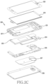
- FIG. 2C is an exploded perspective view of an electronic device.
- the electronic device 220 of FIG. 2C may include a lateral bezel structure 221, a first support member 2211 (e.g., a bracket), a front plate 222, a display 223, a printed circuit board 224, a battery 225, a second support member 226 (e.g., a rear case), an antenna 227, and a rear plate 228.
- the electronic device 220 may omit at least one (e.g., the first support member 2211 or the second support member 226) of the constituent elements, or additionally include another constituent element.
- At least one of the constituent elements of the electronic device 220 may be identical or similar to at least one of the constituent elements of the electronic device 200 of FIG. 2A or 2B , and a duplicate description thereof will be omitted below.
- the first support member 2211 may be disposed inside the electronic device 220 and be connected with the lateral bezel structure 221, or be formed integrally with the lateral bezel structure 221.
- the first support member 2211 may be formed of, for instance, a metallic material and/or a non-metallic material (e.g., a polymer material).
- the first support member 2211 may be joined with the display 223 on one surface thereof, and the printed circuit board 224 on the other surface thereof.
- a processor, a memory, and/or an interface may be mounted on the printed circuit board 224.
- the processor may include, for instance, one or more of a central processing unit, an application processor, a graphic processing unit, an image signal processor, a sensor hub processor, or a communication processor.
- the memory may include, for instance, a volatile memory or a non-volatile memory.
- the Interface may include, for instance, a high definition multimedia interface (HDMI), a universal serial bus (USB) interface, an SD card interface, and/or an audio interface.
- HDMI high definition multimedia interface
- USB universal serial bus
- the interface may electrically or physically connect the electronic device 220 with an external electronic device, and include a USB connector, an SD card/MMC connector, or an audio connector.
- the battery 225 is a unit for supplying power to at least one constituent element of the electronic device 220, and may include a non-rechargeable (primary) battery, a rechargeable (secondary) battery, or a fuel cell.
- a non-rechargeable (primary) battery for example, at least a part of the battery 225 may be disposed in substantially the same plane as the printed circuit board 224.
- the battery 225 may be integrally disposed inside the electronic device 220, or be disposed to be detachable from the electronic device 220.
- the antenna 227 may be disposed between the rear plate 228 and the battery 225.
- the antenna 227 may include, for instance, a near field communication (NFC) antenna, a wireless charging antenna, and/or a magnetic secure transmission (MST) antenna.
- NFC near field communication
- MST magnetic secure transmission
- the antenna 227 may perform near field communication with an external device, or may wirelessly transmit/receive power required for charging.
- an antenna structure may be obtained by some of the lateral bezel structure 221 and/or the first support member 2211, or a combination thereof.
- FIG. 3A is a view illustrating an example of an electronic device supporting 5G communication.
- an electronic device 300 may include a housing 310, a processor 340, a communication module 350 (e.g., the communication module 190 of FIG. 1 ), a first communication unit 321, a second communication unit 322, a third communication unit 323, a fourth communication unit 324, a first conductive line 331, a second conductive line 332, a third conductive line 333, or a fourth conductive line 334.
- a communication module 350 e.g., the communication module 190 of FIG. 1
- a first communication unit 321, a second communication unit 322, a third communication unit 323, a fourth communication unit 324 e.g., the communication module 190 of FIG. 1
- a first communication unit 321, a second communication unit 322, a third communication unit 323, a fourth communication unit 324 e.g., the communication module 190 of FIG. 1
- a first communication unit 321, a second communication unit 322, a third communication unit 323, a fourth communication unit 324 e.g., the communication
- the housing 310 may protect the other constituent elements of the electronic device 300.
- the housing 310 may include, for instance, a front plate, a rear plate (a back plate) that faces away from the front plate, and a lateral member (or a metal frame) that is attached to the rear plate or is formed integrally with the rear plate, and surrounds a space between the front plate and the rear plate.
- the electronic device 300 may include a first communication unit 321, a second communication unit 322, a third communication unit 323, or a fourth communication unit 324.
- the first communication unit 321, the second communication unit 322, the third communication unit 323, or the fourth communication unit 324 may be located inside the housing 310.
- the first communication unit 321 may be disposed at a left upper end of the electronic device 300
- the second communication unit 322 may be disposed at a right upper end of the electronic device 300
- the third communication unit 323 may be disposed at a left lower end of the electronic device 300
- the fourth communication unit 324 may be disposed at a right lower end of the electronic device 300.
- the processor 340 may include one or more of a central processing unit, an application processor, a graphic processing unit (GPU), an image signal processor of a camera, or a baseband processor (or a communication processor (CP)).
- the processor 340 may be implemented by a system-on-chip (SoC) or a system-in-package (SiP).
- SoC system-on-chip
- SiP system-in-package
- the communication module 350 may be electrically connected with the first communication unit 321, the second communication unit 322, the third communication unit 323, or the fourth communication unit 324 using the first conductive line 331, the second conductive line 332, the third conductive line 333, or the fourth conductive line 334.
- the communication module 350 may include, for instance, a baseband processor, or at least one communication circuit (e.g., an IFIC or an RFIC).
- the communication module 350 may include, for instance, a baseband processor independent of the processor 340 (e.g., the application processor (AP)).
- the first conductive line 331, the second conductive line 332, the third conductive line 333, or the fourth conductive line 334 may include, for instance, a coaxial cable or an FPCB.
- the communication module 350 may include a first baseband processor (BP) (not illustrated) or a second BP (not illustrated).
- the electronic device 300 may further include one or more interfaces for supporting inter-chip communication between the first BP (or the second BP) and the processor 340.
- the processor 340 and the first BP or second BP may transmit/receive data using the inter-chip interface (an inter-processor communication channel) .
- the first BP or the second BP may provide an interface for performing communication with other individual entities.
- the first BP may support wireless communication for a first network (not illustrated).
- the second BP may support wireless communication for a second network (not illustrated).
- the first BP or the second BP may form one module along with the processor 340.
- the first BP or the second BP may be formed integrally with the processor 340.
- the first BP or the second BP may be disposed in one chip or be formed in an independent chip type.
- the processor 340 and at least one BP e.g., the first BP
- SoC SoC
- the other BP e.g., the second BP
- the first network (not illustrated) or the second network (not illustrated) may correspond to the network 199 of FIG. 1 .
- the first network (not illustrated) and the second network (not illustrated) may include a 4th generation (4G) network and a 5th generation (5G) network, respectively.
- the 4G network may support, for instance, the long-term evolution (LTE) protocol regulated in 3GPP.
- the 5G network may support, for instance, the new radio (NR) protocol regulated in 3GPP.
- FIG. 3B is a block diagram of a communication unit.
- a communication unit 360 may include a communication circuit 362 (e.g., an RFIC), a printed circuit board (PCB) 361, a first antenna array 363, or a second antenna array 364.
- a communication circuit 362 e.g., an RFIC
- PCB printed circuit board
- the communication circuit 362, the first antenna array 363, or the second antenna array 364 may be located on the PCB 361.
- the first antenna array 363 or the second antenna array 364 may be disposed on a first surface of the PCB 361, and the communication circuit 362 may be located on a second surface of the PCB 361.
- the PCB 361 may include a connector (e.g., a coaxial cable connector or a board-to-board (B-to-B)) for electrical connection with another PCB (e.g., a PCB on which the communication module 350 of FIG. 3A is disposed) using a transmission line (e.g., the first conductive line 331 of FIG. 3A or a coaxial cable).
- the PCB 361 may be connected with the PCB on which the communication module 350 is disposed via a coaxial cable using a coaxial cable connector, and the coaxial cable may be used to transmit transmitting and receiving IF or RF signals.
- power or other control signals may be transmitted through a B-to-B connector.
- the first antenna array 363 or the second antenna array 364 may include a plurality of antenna elements.
- the antenna elements may include patch antennas, loop antennas, or dipole antennas.
- the antenna element included in the first antenna array 363 may be a patch antenna to produce a beam toward the rear plate of the electronic device 360.
- the antenna element included in the second antenna array 364 may be a dipole antenna or a loop antenna to produce a beam toward the lateral member of the electronic device (e.g., the electronic device 200 of FIG. 2A ).
- the communication circuit 362 may support at least some (e.g., about 24 to 30 GHz, or about 37 to 40 GHz) of about 3 to 100 GHz bands.
- the communication circuit 362 may perform frequency up- or down-conversion.
- the communication circuit 362 included in the communication unit 360 e.g., the first communication unit 321 of FIG. 3A
- the communication circuit 362 included in the communication unit 360 e.g., the first communication unit 321 of FIG.
- the 3A may down-convert an RF signal (e.g., a millimeter wave signal) received through the first antenna array 363 or the second antenna array 364 into an IF signal, and transmit the IF signal to the communication module using the conductive line.
- an RF signal e.g., a millimeter wave signal
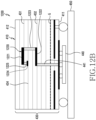
- FIG. 4A is a perspective view of a communication unit .
- FIG. 4B is a sectional view illustrating a stacked structure of the communication unit of FIG. 4A .
- the communication unit 400 of FIG. 4A may be at least partly similar to the communication unit 310, 320, 330, or 340 of FIG. 3 .
- the communication unit 400 may include an antenna structure.
- the antenna structure may include a board 410 and a loop antenna 420 that is disposed in a partial region of the board 410.
- the communication unit 400 may include a board 410.
- the board 410 may include a first surface 411 and a second surface 412 that faces away from the first surface 411.
- the board 410 may be disposed such that the second surface 412 thereof faces the rear plate (e.g., the rear plate 211 of FIG. 2B ) of the electronic device (e.g., the electronic device 200 of FIG. 2B ).
- the board 410 may be disposed such that the second surface 412 thereof faces the lateral member (e.g., the lateral member 216 of FIG. 2A ) or the front plate (e.g., the front plate 202 of FIG. 2A ) of the electronic device.
- the board 410 may include a loop antenna 420 that is substantially disposed in an edge region of the board 410.
- the loop antenna 420 may include a first conductive pattern 421, a second conductive pattern 422, or a third conductive pattern 423 that are electrically connected to one another.
- the communication unit 400 may include a wireless communication circuit 440 that is disposed on the first surface 411 of the board 410.
- the wireless communication circuit 440 may be set to transmit/receive signals having frequencies of a range of about 3 GHz to 100 GHz.
- the board 410 may be mounted on the PCB (e.g., the PCB 350 of FIG. 3 ) of the electronic device (e.g., the electronic device 300 of FIG. 3 ) in a ball grid array (BGA) package type.
- BGA ball grid array
- At least a part of the loop antenna 420 may be disposed on a plurality of insulating layers 430, inclusive of the first surface 411 and/or the second surface 412 of the board 410.
- the loop antenna 420 may be disposed between the plurality of insulating layers 430 that form the board 410, rather than the first surface 411 and the second surface 412 of the board 410.
- a distance between at least some of the plurality of insulating layers 430 contributing to a thickness of the board 410 may be used as an electric length (e.g., a radiation path) for the loop antenna 420.
- the loop antenna 420 may include a first conductive pattern 421 that is disposed on a first plane 431 of any one of the plurality of insulating layers 430, a second conductive pattern 422 that is disposed on a second plane 432 parallel to the first plane 431, and a third conductive pattern 423 that is spaced apart from the second conductive pattern 422 at a constant interval and is disposed on the second plane 432.
- the second conductive pattern 422 and the third conductive pattern 423 are disposed on the same plane (e.g., the second plane 432), but not limited thereto.
- the second conductive pattern 422 and the third conductive pattern 423 may be disposed on different planes that are parallel to each other or are not parallel to each other.
- the second plane 432 is disposed parallel to the first plane 431, but it is not disposed on the same plane.
- One end 4211 of the first conductive pattern 421 may be electrically connected with one end 4221 of the second conductive pattern 422 through a first conductive via 424 that is formed in such a way as to pass through at least some of the plurality of insulating layers 430 in a longitudinal direction (e.g., a thickness direction of the board).
- the other end 4212 of the first conductive pattern 421 may be electrically connected with one end 4231 of the third conductive pattern 423 through a second conductive via 425 that is formed in such a way as to pass through at least some of the plurality of insulating layers 430 in a longitudinal direction.
- the other end 4222 of the second conductive pattern 422 may be electrically connected to a ground plane G of the board 410.
- the other end 4232 of the third conductive pattern 423 may be electrically connected to the wireless communication circuit 440 disposed on the first surface 411 of the board 410.
- the second conductive pattern 422 and the ground plane G may be electrically connected through a grounding via 442.
- the third conductive pattern 423 and the wireless communication circuit 440 may also be electrically connected through a power-supplying via 441.
- the loop antenna 420 may be operated as a loop type antenna having a radiation path (e.g., a path 1) that is supplied with power from the other end 4232 of the third conductive pattern 423 and is connected to the ground plane G of the board 410 through the second conductive via 425, the first conductive pattern 421, the first conductive via 424, and the second conductive pattern 422.
- a radiation path e.g., a path 1
- the loop antenna 420 has a radiation path opposite to the above-mentioned radiation path even if a power-supplying position and a grounding position are exchanged with each other, and thereby the same radiation performance can be ensured.
- the loop antenna 420 may adjust a working frequency band and bandwidth according to a length and width of the first conductive pattern 421 and/or a length and width or interval of each of the second and third conductive patterns 422 and 423, and thus an electric length adjusted according to lengths of the conductive vias 424 and 425. Since the loop antenna 420 may be substantially disposed in the edge region of the board 410 in the thickness direction of the board 410 using at least some of the plurality of insulating layers 430 of the board 410, radiation performance degradation of the antenna caused by the conductive elements disposed around the board 410 can be reduced.
- the conductive vias 424 and 425 are disposed in the edge region of the board 410 and the distance between the plurality of insulating layers 430 contributing to the thickness of the board 410 is used as the electric length (e.g., the radiation path) for the loop antenna 420, lateral radiation performance can be improved.
- the conductive vias 424 and 425 are disposed in the edge region of the board 410 and the distance between at least some of the plurality of insulating layers 430 contributing to the thickness of the board 410 is used as the electric length (e.g., the radiation path) for the loop antenna 420, lateral radiation performance can be improved.
- FIG. 4C is a perspective view of a communication unit.
- the communication unit 400 of FIG. 4C may have a configuration that is generally similar to that of the communication unit 400 of FIG. 4A , and only a connecting member for electrically connecting the first conductive pattern 421, the second conductive pattern 422, and the third conductive pattern 423 may be modified.
- the communication unit 400 may have the same radiation path as the communication unit 400 of FIG. 4A .
- the communication unit 400 may include an antenna structure.
- the antenna structure may include a board 410 and a loop antenna 420 that is disposed in a partial region of the board 410.
- the communication unit 400 may include a board 410.
- the board 410 may include a first surface 411, a second surface 412 that faces away from the first surface 411, and a lateral surface 413 that surrounds a space between the first surface 411 and the second surface 412.
- the board 410 may be disposed such that the second surface 412 thereof faces the rear plate (e.g., the rear plate 211 of FIG. 2B ) of the electronic device (e.g., the electronic device 200 of FIG. 2B ).
- the board 410 may include a loop antenna 420 that is substantially disposed in an edge region of the board 410.
- the loop antenna 420 may include a first conductive pattern 421, a second conductive pattern 422, or a third conductive pattern 423 that are electrically connected to one another.
- the communication unit 400 may include a wireless communication circuit 440 that is disposed on the first surface 411 of the board 410.
- the board 410 may be mounted on the PCB (e.g., the PCB 350 of FIG. 3 ) of the electronic device (e.g., the electronic device 300 of FIG. 3 ) in a ball grid array (BGA) package type.
- BGA ball grid array
- the board 410 may include conductive lateral connecting members 461 and 462 that are disposed on the lateral surface 413 to electrically connect the first conductive pattern 421 and the second conductive pattern 422 and to electrically connect the first conductive pattern 421 and the third conductive pattern 423.
- At least a part of the loop antenna 420 may be disposed on a plurality of insulating layers 430, inclusive of the first surface 411 and/or the second surface 412 of the board 410.
- the loop antenna 420 may be disposed between the plurality of insulating layers 430 that form the board 410, rather than the first surface 411 and the second surface 412 of the board 410.
- a distance between at least some of the plurality of insulating layers 430 contributing to a thickness of the board 410 may be used as an electric length (e.g., a radiation path) for the loop antenna 420.
- the loop antenna 420 may include a first conductive pattern 421 that is disposed on a first plane 431 of any one of the plurality of insulating layers 430, a second conductive pattern 422 that is disposed on a second plane 432 parallel to the first plane 431, and a third conductive pattern 423 that is spaced apart from the second conductive pattern 422 at a constant interval and is disposed on the second plane 432.
- the second conductive pattern 422 and the third conductive pattern 423 are disposed on the same plane (e.g., the second plane 432), but not limited thereto.
- the second conductive pattern 422 and the third conductive pattern 423 may be disposed on different planes that are parallel to each other or are not parallel to each other.
- the second plane 432 is disposed parallel to the first plane 431, but it is not disposed on the same plane.
- One end 4211 of the first conductive pattern 421 may be electrically connected with one end 4221 of the second conductive pattern 422 through a first conductive lateral connecting member 461 disposed on the lateral surface 413 of the board 410.
- the other end 4212 of the first conductive pattern 421 may be electrically connected with one end 4231 of the third conductive pattern 423 through a second conductive lateral connecting member 462 disposed on the lateral surface 413 of the board 410.
- the other end 4222 of the second conductive pattern 422 may be electrically connected to a ground plane G of the board 410.
- the other end 4232 of the third conductive pattern 423 may be electrically connected to the wireless communication circuit 440 disposed on the first surface 411 of the board 410.
- the second conductive pattern 422 and the ground plane G may be electrically connected through a grounding via (e.g., the grounding via 442 of FIG. 4B ).
- the third conductive pattern 423 and the wireless communication circuit 440 may also be electrically connected through a power-supplying via (e.g., the power-supplying via 441 of FIG. 4B ) .
- the first conductive lateral connecting member 461 and the second conductive lateral connecting member 462 may include a plating member (e.g., a Cu plating) that is disposed on the lateral surface 413 of the board 410, or a conductive paint that is applied to the lateral surface of the board.
- a plating member e.g., a Cu plating
- a conductive paint that is applied to the lateral surface of the board.
- FIG. 5A is a view illustrating a radiation pattern 510 of the communication unit 400 of FIG. 4A . It can be found that a beam pattern (an endfire) is produced in a lateral direction of the board by a loop antenna.
- FIGS. 5B and 5C are graphs illustrating a reflection coefficient and gain of the communication unit 400 of FIG. 4A . It can be found that the loop antenna shows resonance characteristics of -19 dB or higher at S11 (e.g., a region 520 of FIG. 5B ), and shows a 5 dB gain higher than a result of a dipole antenna structure having the same board structure and physical property conditions by 2.5 dB (e.g., a region 530 of FIG. 5C ) .
- FIG. 6 is a perspective view of a communication unit.
- the communication unit 600 of FIG. 6 may be at least partly similar to the communication unit 310, 320, 330, or 340 of FIG. 3 .
- the communication unit 600 may include a first surface 611 and a second surface 612 that faces away from the first surface 611.
- the communication unit 600 may include a wireless communication circuit 640 that is mounted on the first surface 611 of a board 610.
- the communication unit 600 may include a first loop antenna 621, a second loop antenna 622, a third loop antenna 623, or a fourth loop antenna 624 that are disposed antenna elements in a substantially edge region of the board 610 at fixed intervals, and the wireless communication circuit 640 that is electrically connected with the first loop antenna 621, the second loop antenna 622, the third loop antenna 623, or the fourth loop antenna 624.
- the communication unit 600 may be set to transmit/receive at least one signal having a frequency band of a range of about 3 GHz to 100 GHz through the wireless communication circuit 640 and an antenna array that includes the first loop antenna 621, the second loop antenna 622, the third loop antenna 623, or the fourth loop antenna 624.
- the first loop antenna 621, the second loop antenna 622, the third loop antenna 623, or the fourth loop antenna 624 of the communication unit 600 may be formed through at least one conductive pattern (e.g., the first conductive pattern 421, the second conductive pattern 422, or the third conductive pattern 423 of FIG. 4A ), and a conductive via (e.g., the first conductive via 424 or the second conductive via 425 of FIG. 4A ) in a way that is at least partly similar to a configuration of the above-mentioned loop antenna of FIG. 4A (e.g., the loop antenna 420 of FIG. 4A ).
- a conductive via e.g., the first conductive via 424 or the second conductive via 425 of FIG. 4A
- FIG. 7A is a view illustrating a radiation pattern 710 of the communication unit 600 of FIG. 6 . It can be found that a bandwidth is relatively wider than an antenna array having the same board structure and physical property conditions.
- FIGS. 7B and 7C are graphs illustrating a reflection coefficient and gain of the communication unit 600 of FIG. 6 .
- a loop antenna array shows resonance characteristics of - 20 dB or higher at S11 (e.g., a region 720 of FIG. 7B ).
- FIG. 7C illustrates gain characteristics obtained by performing simulation on an elevation direction (theta) of the loop antenna array. It can be found that, in comparison with simulation results of a dipole array structure having the same board structure and physical property conditions, a peak gain increases 0.8 dB from 9.3 dB to 10.13 dB, and a 3-dB bandwidth increases 60° from 90° to 150° (e.g., a region 730 of FIG. 7C ).
- FIG. 8A is a perspective view of a communication unit according to various embodiments of the disclosure.
- FIG. 8B is a sectional view illustrating a stacked structure of the communication unit of FIG. 8A according to various embodiments of the disclosure.
- the communication unit 800 of FIG. 8A may be at least partly similar to the communication units 310, 320, 330, and 340 of FIG. 3 .
- the same reference signs are used for constituent elements identical or similar to those of the communication unit 400 of FIGS. 4A and 4B .
- the communication unit 800 includes a board 410.
- the board 410 includes a first surface 411 and a second surface 412 that faces away from the first surface 411.
- the board 410 includes a loop antenna 820 that is substantially disposed in an edge region of the board 410.
- the loop antenna 820 includes a first conductive pattern 421, a second conductive pattern 422, a third conductive pattern 423, and a fourth conductive pattern 426 that are electrically connected to one another.
- the communication unit 400 includes a wireless communication circuit 440 that is disposed on the first surface 411 of the board 410.
- the wireless communication circuit 440 is set to transmit/receive signals having frequencies of a range of about 3 GHz to 100 GHz.
- At least a part of the loop antenna 820 is disposed on a plurality of insulating layers 430, inclusive of the first surface 411 and/or the second surface 412 of the board 410.
- the loop antenna 820 is disposed between the plurality of insulating layers 430 that form the board 410, rather than the first surface 411 and the second surface 412 of the board 410.
- a distance between at least some of the plurality of insulating layers 430 included in the board 410 is used as an electric length (e.g., a radiation path) for the loop antenna 820.
- the loop antenna 820 includes a first conductive pattern 421 that is disposed on a first plane 431 of any one of the plurality of insulating layers 430, a second conductive pattern 422 that is disposed on a second plane 432 parallel to the first plane 431, a third conductive pattern 423 that is spaced apart from the second conductive pattern 422 at a constant interval and is disposed on the second plane 432, and a fourth conductive pattern 426 that is disposed on a third plane 433 parallel to the first plane 431.
- the second conductive pattern 422 and the third conductive pattern 423 are disposed on the same plane (e.g., the second plane 432).
- the first plane 431, the second plane 432, and the third plane 433 are disposed parallel to one another, and are not disposed on the same plane. According to an embodiment, the first plane 431 is disposed between the second plane 432 and the third plane 433.
- one end 4211 of the first conductive pattern 421 is electrically connected with one end 4221 of the second conductive pattern 422 through a first conductive via 424 that is formed in such a way as to pass through at least some of the plurality of insulating layers 430 in a longitudinal direction (a thickness direction of the board).
- the other end 4212 of the first conductive pattern 421 is electrically connected with one end 4231 of the third conductive pattern 423 through a second conductive via 425 that is formed in such a way as to pass through at least some of the plurality of insulating layers 430 in a longitudinal direction.
- one end 4261 of the fourth conductive pattern 426 is electrically connected to the other end 4212 of the first conductive pattern 421 through a third conductive via 427 that is formed in such a way as to pass through at least some of the plurality of insulating layers 430 in a longitudinal direction.
- the second conductive via 425 and the third conductive via 427 may be disposed to be aligned in a row in the longitudinal direction (the thickness direction) of the board 410.
- the other end 4222 of the second conductive pattern 422 and the other end 4262 of the fourth conductive pattern 426 may be electrically connected to a ground plane G of the board 410.
- the other end 4232 of the third conductive pattern 423 may be electrically connected to the wireless communication circuit 440 disposed on the first surface 411 of the board 410.
- the second conductive pattern 422, the fourth conductive pattern 426, and the ground plane G may be electrically connected through a grounding via 442.
- the third conductive pattern 423 and the wireless communication circuit 440 may also be electrically connected through a power-supplying via 441.
- the loop antenna 820 may be operated as a dual-band antenna having working frequency bands different from each other.
- the loop antenna 820 may be operated as a loop type antenna having a first radiation path (e.g., a path 1) that is supplied with power from the other end 4232 of the third conductive pattern 423 and is connected to the ground plane G of the board 410 through the second conductive via 425, the first conductive pattern 421, the first conductive via 424, and the second conductive pattern 422.
- a first radiation path e.g., a path 1
- the loop antenna 820 may be operated as a loop type antenna having a second radiation path (e.g., a path 2) that is supplied with power from the other end 4232 of the third conductive pattern 423 and is connected to the ground plane G of the board 410 through the second conductive via 425, the third conductive via 427, and the fourth conductive pattern 426.
- the wireless communication circuit 440 may be set to transmit/receive a first signal having a first frequency using the first radiation path (the path 1), and to transmit/receive a second signal having a second frequency different from the first frequency using the second radiation path (the path 2).
- the first frequency may include a lower frequency band than the second frequency.
- the first frequency may include frequencies of a range of about 24 GHz to 32 GHz
- the second frequency may include frequencies of a range of about 34 GHz to 44 GHz.
- the loop antenna 820 may adjust a working frequency band and bandwidth according to a length and width of the first conductive pattern 421 and/or a length and width or interval of each of the second and third conductive patterns 422 and 423, a length and width of the fourth conductive pattern 426, and thus an electric length adjusted according to lengths of the conductive vias 424, 425, and 427.
- the loop antenna 820 since the loop antenna 820 ia substantially disposed in the edge region of the board 410 in the thickness direction of the board 410 using the plurality of insulating layers 430 of the board 410, radiation performance degradation of the antenna caused by the conductive elements disposed around the board 410 can be reduced.
- the conductive vias 424, 425, and 427 are disposed in the edge region of the board 410 and uses the distance between at least some of the plurality of insulating layers 430 utilized as a thickness is used as the electric length (e.g., the radiation path) for the loop antenna 820, lateral radiation performance can be improved.
- a loop antenna may have the same structure as the loop antenna 820 of FIG. 8A , and be configured to have another radiation path by exchanging a power-supplying position and a grounding position.
- the loop antenna may be operated as a dual-band antenna having working frequency bands different from each other.
- the loop antenna may be operated as a loop type antenna having a first radiation path that is supplied with power from the other end 4222 of the second conductive pattern 422 and is connected to the ground plane G of the board 410 through the first conductive via 424, the first conductive pattern 421, the second conductive via 425, and the third conductive pattern 423.
- the loop antenna may be operated as a loop type antenna having a second radiation path that is supplied with power from the other end 4262 of the fourth conductive pattern 426 and is connected to the ground plane G of the board 410 through the third conductive via 427, the second conductive via 425, and the third conductive pattern 423.
- the wireless communication circuit 440 may be set to transmit/receive a first signal having a first frequency using the first radiation path, and to transmit/receive a second signal having a second frequency different from the first frequency using the second radiation path.
- the first frequency may include a lower frequency band than the second frequency.
- the first frequency may include frequencies of a range of about 24 GHz to 32 GHz
- the second frequency may include frequencies of a range of about 34 GHz to 44 GHz.
- the conductive vias 424, 425, and 427 are disposed in the edge region of the board 410 and uses the distance between at least some of the plurality of insulating layers 430 utilized as a thickness is used as the electric length (e.g., the radiation path) for the loop antenna, lateral radiation performance can be improved.
- the loop antenna 820 of FIG. 8A may include the above-mentioned conductive lateral connecting members of FIG. 4C (e.g., the conductive lateral connecting members 461 and 462 of FIG. 4C ) disposed on the lateral surface (e.g., the lateral surface 413 of FIG. 4C ) of the board 410 instead of the conductive vias 424, 425, and 427.
- the conductive lateral connecting members of FIG. 4C e.g., the conductive lateral connecting members 461 and 462 of FIG. 4C
- the lateral surface e.g., the lateral surface 413 of FIG. 4C
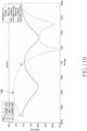
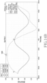
- FIG. 9 is a graph illustrating a reflection coefficient of the communication unit 820 of FIG. 8A according to various embodiments of the disclosure. It can be found that a resonance point is formed at a first working frequency of about 21.6 GHz (e.g., a region 910 of FIG. 9 ), and a resonance point is formed at a second working frequency of about 28.8 GHz (e.g., a region 920 of FIG. 9 ).
- FIG. 10 is a perspective view of a communication unit.
- the communication unit 1000 of FIG. 10 may be at least partly similar to the communication units 310, 320, 330, and 340 of FIG. 3 .
- the same reference signs are used for constituent elements identical or similar to those of the communication unit 400 of FIGS. 4A and 4B .
- the communication unit 1000 may include a board 410.
- the board 410 may include a first surface 411 and a second surface 412 that faces away from the first surface 411.
- the board 410 may include a loop antenna 1020.
- the loop antenna 1020 may include a first conductive pattern 421, a second conductive pattern 422, or a third conductive pattern 423 that are electrically connected to one another through a first conductive via 424 or a second conductive via 425.
- the communication unit 1000 may include a wireless communication circuit 440 that is disposed on a first surface 411 of the board 410.
- the wireless communication circuit 440 may be set to transmit/receive signals having frequencies of a range of about 3 GHz to 100 GHz.
- the loop antenna 1020 may be operated as a loop type antenna having a radiation path (e.g., the radiation path (the path O) of FIG. 4A ) that is supplied with power from the third conductive pattern 423 and is connected to a ground plane G of the board 410 through the second conductive via 425, the first conductive pattern 421, the first conductive via 424, and the second conductive pattern 422.
- a radiation path e.g., the radiation path (the path O) of FIG. 4A
- the loop antenna 1020 may include a conductive director 460 that is disposed in such a way as to at least partly overlap the conductive patterns 421, 422, and 423 used as antenna elements in a direction in which a beam pattern is formed.
- the conductive director 460 may be disposed at a position corresponding to a lateral surface that surrounds a space between the first surface 411 and the second surface 412 of the board 410.
- the conductive director 460 may be disposed inside an electronic device (e.g., the electronic device 300 of FIG. 3 ) in place so as to have a distance capable of reacting with the conductive patterns 421, 422, and 423.
- the conductive director 460 may be disposed in various surrounding structures such as a PCB (e.g., the PCB 350 of FIG. 3 ) disposed inside the electronic device (e.g., the electronic device 300 of FIG. 3 ) or a housing (e.g., the housing 210 of FIG. 2A ).
- the conductive director 460 may include an EMI paint, a metal plate, or a FPCB that is disposed on an inner surface of the housing.
- the conductive director 460 may be insert-molded in the housing (e.g., the housing 210 of FIG. 2A ).
- the conductive director 460 may be disposed in such a way as to be attached to the outside of the housing (e.g., the housing 210 of FIG. 2A ).
- the conductive director 460 may include a conductive decorating member that is disposed on an outer surface of the housing (e.g., the housing 210 of FIG. 2A ).
- the conductive director 460 may be formed in a size above the longest length of lengths of the conductive patterns 421, 422, and 423, and may be disposed to maintain a proper distance from the conductive patterns according to the working frequency.
- the loop antenna 1020 of FIG. 10 may include the above-mentioned conductive lateral connecting members of FIG. 4C (e.g., the conductive lateral connecting members 461 and 462 of FIG. 4C ) that are disposed on the lateral surface (e.g., the lateral surface 413 of FIG. 4C ) of the board 410 instead of the conductive vias 424 and 425.
- the conductive lateral connecting members of FIG. 4C e.g., the conductive lateral connecting members 461 and 462 of FIG. 4C
- the lateral surface e.g., the lateral surface 413 of FIG. 4C
- FIG. 11A is a view illustrating a radiation pattern 1110 of the communication unit 1020 of FIG. 10 . It can be found that a greater gain and a shaper beam pattern are obtained in the loop antenna by the conductive director.
- FIG. 11B is a graph illustrating a reflection coefficient of the communication unit 1020 of FIG. 10 . It can be found that a gain of 6.5 dB is obtained with respect to the elevation direction (theta), and an effect of improving a gain of about 1.5 dB compared to the existing gain is obtained (e.g., a region 1120 of FIG. 11B ).
- FIG. 12A is a perspective view of a communication unit.
- FIG. 12B is a sectional view illustrating a stacked structure of the communication unit of FIG. 12A .
- the communication unit 1200 of FIG. 12A may be at least partly similar to the communication units 310, 320, 330, and 340 of FIG. 3 .
- the same reference signs are used for constituent elements identical or similar to those of the communication unit 400 of FIGS. 4A and 4B .
- the communication unit 1200 may include a board 410.
- the board 410 may include a first surface 411 and a second surface 412 that faces away from the first surface 411.
- the board 410 may include a loop antenna 1220 that is substantially disposed in an edge region of the board 410.
- the loop antenna 1220 may include a first conductive pattern 1221, a second conductive pattern 1222, or a third conductive pattern 1224 that are electrically connected to one another.
- the communication unit 1200 may include a wireless communication circuit 440 that is disposed on the first surface 411 of the board 410.
- the wireless communication circuit 440 may be set to transmit/receive signals having frequencies of a range of about 3 GHz to 100 GHz.
- At least a part of the loop antenna 1220 may be disposed on at least some of a plurality of insulating layers 430, inclusive of the first surface 411 and/or the second surface 412 of the board 410.
- the loop antenna 1220 may be disposed between at least some of the plurality of insulating layers 430 that form the board 410, rather than the first surface 411 and the second surface 412 of the board 410.
- a distance between at least some of the plurality of insulating layers 430 contributing to a thickness of the board 410 may be used as an electric length (e.g., a radiation path) for the loop antenna 1220.
- the loop antenna 1220 may include a first conductive pattern 1221 that is disposed on a first plane 431 of any one of the plurality of insulating layers 430, a second conductive pattern 1222 that is disposed on a second plane 432 parallel to the first plane 431, and a third conductive pattern 1224 that is spaced apart from the second conductive pattern 1222 at a constant interval and is disposed on a fourth plane 434.
- the first plane 431, the second plane 432, and the fourth plane 434 are disposed parallel to one another, and are not disposed on the same plane.
- the fourth plane 434 may be disposed between the first plane 431 and the second plane 432.
- One end 12211 of the first conductive pattern 1221 may be electrically connected with one end 12221 of the second conductive pattern 1222 through a first conductive via 1223 that is formed in such a way as to pass through at least some of the plurality of insulating layers 430 in a longitudinal direction (a thickness direction of the board) .
- the other end 12212 of the first conductive pattern 1221 may be electrically connected with the third conductive pattern 1224 through a second conductive via 1225 that is formed in such a way as to pass through at least some of the plurality of insulating layers 430 in a longitudinal direction.
- the third conductive pattern 1224 may be electrically connected to a ground plane G of the board 410, and the other end 12222 of the second conductive pattern 1222 may be electrically connected to the wireless communication circuit 440 disposed on the first surface 411 of the board 410.
- the third conductive pattern 1224 and the ground plane G may be electrically connected through a grounding via (not illustrated).
- the second conductive pattern 1222 and the wireless communication circuit 440 may also be electrically connected through a power-supplying via 441.
- the loop antenna 1220 may be operated as a loop type antenna having a radiation path (e.g., a path 3) that is supplied with power from the other end 12222 of the second conductive pattern 1222 and is connected to the ground plane G of the board 410 through the first conductive via 1223, the first conductive pattern 1221, the second conductive via 1225, and the third conductive pattern 1224.
- the loop antenna 1220 has a radiation path opposite to the above-mentioned radiation path even if a power-supplying position and a grounding position are exchanged with each other, and thereby the same radiation performance can be ensured.
- a power-supplying portion of the second conductive pattern 1222 and a ground portion of the third conductive pattern 1224 are generally disposed in such a way as to at least partly overlap each other, and thereby a compact loop antenna structure can be implemented.
- the loop antenna 1220 of FIG. 12A may include the above-mentioned conductive lateral connecting members of FIG. 4C (e.g., the conductive lateral connecting members 461 and 462 of FIG. 4C ) that are disposed on the lateral surface (e.g., the lateral surface 413 of FIG. 4C ) of the board 410 instead of the conductive vias 1223 and 1225.
- FIG. 13A is a perspective view of a communication unit.
- FIG. 13B is a sectional view illustrating a stacked structure of the communication unit of FIG. 4A .
- the communication unit 1300 of FIG. 13A may be at least partly similar to the communication units 310, 320, 330, and 340 of FIG. 3 .
- the same reference signs are used for constituent elements identical or similar to those of the communication unit 400 of FIGS. 4A and 4B .
- the communication unit 1300 of FIGS. 13A and 13B may be configured such that an output signal is coupled to a differential loop array structure by disposing the loop antenna 1220 of FIG. 12A in bilateral symmetry and electrically connecting the loop antennas 1220 to a wireless communication circuit 440.
- the communication unit 1300 may include a board 410.
- the board 410 may include a first surface 411 and a second surface 412 that faces away from the first surface 411.
- the board 410 may include a loop antenna 1310 that is substantially disposed in an edge region of the board 410.
- the loop antenna 1310 may include a first loop antenna 1320 and a second loop antenna 1330 that are electrically connected to the wireless communication circuit 440 and are disposed in symmetry with each other.
- the communication unit 1300 may include the wireless communication circuit 440 that is disposed on the first surface 411 of the board 410.
- the wireless communication circuit 440 may be set to transmit/receive signals having frequencies of a range of about 3 GHz to 100 GHz through the first loop antenna 1320 and the second loop antenna 1330.
- At least a part of the loop antenna 1310 may be disposed on at least some of a plurality of insulating layers 430, inclusive of the first surface 411 and/or the second surface 412 of the board 410.
- the loop antenna 1310 may be disposed between at least some of the plurality of insulating layers 430 that form the board 410, rather than the first surface 411 and the second surface 412 of the board 410.
- a distance between at least some of the plurality of insulating layers 430 contributing to a thickness of the board 410 may be used as an electric length (e.g., a radiation path) for the loop antenna 1310.
- the first loop antenna 1320 may include a first conductive pattern 1321 that is disposed on a first plane 431 of any one of the plurality of insulating layers 430, a second conductive pattern 1322 that is disposed on a second plane 432 parallel to the first plane 431, and a third conductive pattern 1324 that is spaced apart from the second conductive pattern 1322 at a constant interval and is disposed on a fourth plane 434.
- the first plane 431, the second plane 432, and the fourth plane 434 are disposed parallel to one another, and are not disposed on the same plane.
- the fourth plane 434 may be disposed between the first plane 431 and the second plane 432.
- the first conductive pattern 1321 may be electrically connected with the second conductive pattern 1322 through a first conductive via 1323 that is formed in such a way as to pass through at least some of the plurality of insulating layers 430 in a longitudinal direction (a thickness direction of the board).
- the first conductive pattern 1321 may be electrically connected with the third conductive pattern 1324 through a second conductive via 1325 that is formed in such a way as to pass through at least some of the plurality of insulating layers 430 in a longitudinal direction.
- the third conductive pattern 1324 may be electrically connected to a ground plane G of the board 410 and, as another example, the second conductive pattern 1322 may be electrically connected to the wireless communication circuit 440 disposed on the first surface 411 of the board 410.
- the third conductive pattern 1324 and the ground plane G may be electrically connected through a grounding via (not illustrated).
- the second conductive pattern 1322 and the wireless communication circuit 440 may also be electrically connected through a power-supplying via 4
- the second loop antenna 1330 may include a fourth conductive pattern 1331 that is disposed on the first plane 431, a fifth conductive pattern 1332 that is disposed on the second plane 432 parallel to the first plane 431, and a sixth conductive pattern 1334 that is spaced apart from the fifth conductive pattern 1332 at a constant interval and is disposed on the fourth plane 434.
- the fourth conductive pattern 1331 may be electrically connected with the fifth conductive pattern 1332 through a third conductive via 1333 that is formed in such a way as to pass through at least some of the plurality of insulating layers 430 in the longitudinal direction (the thickness direction of the board).
- the fourth conductive pattern 1331 may be electrically connected with the sixth conductive pattern 1334 through a fourth conductive via 1335 that is formed in such a way as to pass through at least some of the plurality of insulating layers 430 in the longitudinal direction.
- the sixth conductive pattern 1334 may be electrically connected to the ground plane G of the board 410.
- the fifth conductive pattern 1332 may be electrically connected to the wireless communication circuit 440 disposed on the first surface 411 of the board 410.
- the sixth conductive pattern 1334 and the ground plane G may be electrically connected through a grounding via (not illustrated).
- the fifth conductive pattern 1332 and the wireless communication circuit 440 may also be electrically connected through a power-supplying via 441-2.
- the first loop antenna 1320 may be operated as a loop type antenna having a radiation path that is supplied with power from the second conductive pattern 1322 and is connected to the ground plane G of the board 410 through the first conductive via 1323, the first conductive pattern 1321, the second conductive via 1325, and the third conductive pattern 1324.
- Second loop antenna 1330 may be operated as a loop type antenna having a radiation path that is supplied with power from the fifth conductive pattern 1332 and is connected to the ground plane G of the board 410 through the third conductive via 1333, the fourth conductive pattern 1331, the fourth conductive via 1335, and the sixth conductive pattern 1334.
- the loop antenna 1310 of FIG. 13A may include the above-mentioned conductive lateral connecting members of FIG. 4C (e.g., the conductive lateral connecting members 461 and 462 of FIG. 4C ) that are disposed on the lateral surface (e.g., the lateral surface 413 of FIG. 4C ) of the board 410 instead of the conductive vias 1323, 1325, 1333, and 1335.
- the conductive lateral connecting members of FIG. 4C e.g., the conductive lateral connecting members 461 and 462 of FIG. 4C
- FIGS. 14A and 14B are graphs illustrating a reflection coefficient and gain of the communication unit 1310 of FIG. 13A . It can be found that a loop antenna array shows resonance characteristics of -15 dB or higher at S11 (e.g., a region 1410 of FIG. 14A ). Further, a gain of 4.5 dB within a wide 3-dB bandwidth of about 169° at about 39 GHz can be secured (e.g., a region 1420 of FIG. 14B ).
- FIGS. 15A and 15B are views illustrating a layout of a communication unit according to various embodiments of the disclosure.
- the communication unit is described with the communication unit 600 of FIG. 6 given as an example, but not limited thereto.
- the communication unit of FIGS. 15A and 15B may be replaced with the loop antenna 420 included in the communication unit 400 of FIG. 4A , in an embodiment of the disclosure with the loop antenna 820 included in the communication unit 800 of FIG. 8A , the loop antenna 1020 included in the communication unit 1000 of FIG. 10 , the loop antenna 1220 included in the communication unit 1200 of FIG. 12A , or the loop antenna 1310 included in the communication unit 1300 of FIG. 13A , or a communication unit in which each of the loop antennas is implemented in an array type as in FIG. 6 .
- an electronic device 1500 includes a housing 1510.
- the housing 1510 includes a lateral member 1520.
- at least a partial region of the lateral member 1520 may be formed of a conductive member, be implemented into a unit conductive portion by a nonconductive portion, and be operated as an antenna radiator.
- the housing 1510 includes a first portion 1511 having a first length, a second portion 1512 that extends in a direction perpendicular to the first portion 1511 and has a second length, a third portion 1513 that extends from the second portion 1512 in parallel to the first portion 1511 so as to have the first length, and a fourth portion 1514 that extends from the third portion 1513 in parallel to the second portion 1512 so as to have the second length.
- a first communication unit 600 or a second communication unit 600-1 is disposed in an internal space 1501 of the electronic device 1500.
- the first communication unit 600 or the second communication unit 600-1 may be disposed at at least one corner portion of the electronic device 1500 having a substantially quadrilateral shape.
- a first lateral portion 6101 of the first communication unit 600 may be disposed adjacent to the first portion 1511 of the housing 1510, and a second lateral portion 6102 of the first communication unit 600 may be disposed adjacent to the second portion 1512 of the housing 1510.
- an electric connecting member 650 e.g., a power terminal and/or an RF terminal
- the electric connecting member 650 may be drawn from a third lateral portion 6103 in the center direction of the electronic device 1500.
- the electric connecting member 650 may be formed integrally with the communication unit, or be connected with the communication unit through a separate electric connecting member (e.g., a coaxial cable or an FPCB).
- a first lateral portion 6101 of the second communication unit 600-1 may be disposed adjacent to the fourth portion 1514 of the housing 1510, and a second lateral portion 6102 of the second communication unit 600-1 may be disposed adjacent to the first portion 1511 of the housing 1510.
- the first communication unit 600 may be disposed such that a beam pattern is formed in a direction (e.g., a direction 4) of the first portion 1511 of the electronic device 1500.
- the second communication unit 600-1 may be disposed such that a beam pattern is formed in a direction (e.g., a direction 5) of the fourth portion 1514 of the electronic device 1500.
- the first communication unit 600, the second communication unit 600-1, or a third communication unit 600-2 may be disposed in regions of some corners of the electronic device 1500.
- the first communication unit 600 may be disposed such that a second surface (e.g., the second surface 612 of FIG. 6 ) of a board (e.g., the board 610 of FIG. 6 ) faces the first portion 1511 in substantially the center of the first portion 1511 of the housing 1510.
- a second plate e.g., the second plate 211 of FIG.
- the first communication unit 600 may be disposed in such a way that the first lateral portion 6101 of the board 610 is parallel to the first portion 1511 of the housing 1510.
- the second communication unit 600-1 may be disposed in such a way that the second surface (e.g., the second surface 612 of FIG. 6 ) of the board (e.g., the board 610 of FIG. 6 ) is adjacent and parallel to the fourth portion 1514 in a partial region of the fourth portion 1514 of the housing 1510.
- the third communication unit 600-2 may be disposed in such a way that the second surface (e.g., the second surface 612 of FIG. 6 ) of the board (e.g., the board 610 of FIG. 6 ) is adjacent and parallel to the second portion 1512 in a partial region of the second portion 1512 of the housing 1510.
- the first communication unit 600, the second communication unit 600-1, or the third communication unit 600-3 may form a beam pattern in a direction (e.g., a -Z direction of FIG. 2A ) of a rear plate (e.g., the rear plate 211 of FIG. 2A ) of the housing 1510.
- a direction e.g., a -Z direction of FIG. 2A
- a rear plate e.g., the rear plate 211 of FIG. 2A
- the communication units 600, 600-1, and 600-2 illustrated in FIG. 15A and/or FIG. 15B may be disposed at each corner of the electronic device having a substantially rectangular shape, at least a partial region of each edge, or a corner or edge by mixture.
- the communication units 600, 600-1, and 600-2 may be disposed in such various ways that the beam pattern directions of FIGS. 15A and 15B can be mixed inside the electronic device.
- regions of the housing 1510 which correspond to portions where the communication units 600, 600-1, and 600-2 are mounted may be formed of a material (e.g., a dielectric material) other than a conductive material in order to prevent radiation performance degradation of the communication units.
- the corresponding regions of the housing 1510 may be replaced by holes formed in the housing in directions in which the beam patterns of the communication units are formed, or metal periodic structures (e.g., metal grids) through which a beam can pass.
- an electronic device e.g., an electronic device 200 of FIG. 2A
- a housing e.g., a housing 210 of FIG. 2A
- a first plate e.g., a front plate 202 of FIG. 2A
- a second plate e.g., a rear plate 211 of FIG. 2B
- a lateral member e.g., a lateral bezel structure (or a "lateral member" 218 of FIG. 2A
- an antenna structure e.g., a communication unit 400 of FIG.
- the antenna structure includes a plurality of insulating layers (e.g., a plurality of insulating layers 430 of FIG. 4A ) disposed in such a way as to be stacked parallel to the first plate, and an array of loop antennas formed through the insulating layers and/or peripheries of the insulating layers; and a wireless communication circuit that is electrically connected to the loop antennas (e.g., loop antennas 621, 622, 623, and 624 of FIG. 6 ) and is set to transmit/receive a first signal having a first frequency of a range of about 3 GHz to 100 GHz.
- a wireless communication circuit that is electrically connected to the loop antennas (e.g., loop antennas 621, 622, 623, and 624 of FIG. 6 ) and is set to transmit/receive a first signal having a first frequency of a range of about 3 GHz to 100 GHz.
- At least one of the loop antennas includes: a first conductive pattern (e.g., a first conductive pattern 421 of FIG. 4A ) that is disposed on a first plane (e.g., a first plane 431 of FIG. 4A ) parallel to the insulating layers; a second conductive pattern (e.g., a second conductive pattern 422 of FIG. 4A ) that is disposed on a second plane (e.g., a second plane 432 of FIG. 4A ) parallel to the first plane; a third conductive pattern (e.g., a third conductive pattern 423 of FIG.
- a first conductive pattern e.g., a first conductive pattern 421 of FIG. 4A
- a first plane e.g., a first plane 431 of FIG. 4A
- a second conductive pattern e.g., a second conductive pattern 422 of FIG. 4A
- a third conductive pattern e.g., a third conductive pattern
- a first conductive via e.g., a first conductive via 424 of FIG. 4A
- a second conductive via e.g., a second conductive via 425 of FIG. 4A
- the at least one of the loop antennas further includes: a fourth conductive pattern (e.g., a fourth conductive pattern 426 of FIG. 8A ) that is disposed on a third plane (e.g., a third plane 433 of FIG. 8A ) parallel to the first plane, wherein the first plane is interposed between the second plane and the third plane; and a third conductive via (e.g., a third conductive via 427 of FIG. 8A ) that electrically connects the first conductive pattern and the fourth conductive pattern through the insulating layers.
- a fourth conductive pattern e.g., a fourth conductive pattern 426 of FIG. 8A
- a third plane e.g., a third plane 433 of FIG. 8A
- a third conductive via e.g., a third conductive via 427 of FIG. 8A
- the third conductive via may be aligned with the second conductive via in a row.
- the wireless communication circuit may be set to transmit/receive a second signal having a second frequency different from the first frequency.
- the electronic device may further include a ground plane (e.g., a ground plane G of FIG. 4B ) formed through the insulating layers and/or the peripheries of the insulating layers, wherein the third conductive pattern may be electrically connected to the wireless communication circuit, and the second conductive pattern and the fourth conductive pattern may be electrically connected to the ground plane.
- a ground plane e.g., a ground plane G of FIG. 4B
- the wireless communication circuit may transmit/receive the first signal using a loop type radiation path that is connected to the ground plane through the third conductive pattern, the second conductive via, the first conductive pattern, the first conductive via, and the second conductive pattern.
- the wireless communication circuit may transmit/receive the second signal using a loop type radiation path that is connected to the ground plane through the third conductive pattern, the second conductive via, the third conductive via, and the fourth conductive pattern.
- the electronic device may further include a ground plane formed through the insulating layers and/or the peripheries of the insulating layers, wherein the third conductive pattern may be electrically connected to the wireless communication circuit, and the second conductive pattern may be electrically connected to the ground plane.
- At least one of the loop antennas includes: a first conductive pattern (e.g., a first conductive pattern 1221 of FIG. 12A ) that is disposed on a first plane parallel to the insulating layers; a second conductive pattern (e.g., a second conductive pattern 1222 of FIG. 12A ) that is disposed on a second plane parallel to the first plane; a third conductive pattern (e.g., a third conductive pattern 1224 of FIG. 12A ) that is disposed on a third plane (e.g., a third plane 434 of FIG. 12A ) between the first plane and the second plane; a first conductive via (e.g., a first conductive via 1223 of FIG.
- a first conductive pattern e.g., a first conductive pattern 1221 of FIG. 12A
- a second conductive pattern e.g., a second conductive pattern 1222 of FIG. 12A
- a third conductive pattern e.g., a third
- a second conductive via (e.g., a second conductive via 1225 of FIG. 12A ) that electrically connects the first conductive pattern and the third conductive pattern through the insulating layers.
- the electronic device may further include a ground plane formed through the insulating layers and/or the peripheries of the insulating layers, wherein the second conductive pattern may be electrically connected to the wireless communication circuit, and the third conductive pattern may be electrically connected to the ground plane.
- a first point of the second conductive pattern which is connected with the wireless communication circuit may be disposed to at least partly overlap a second point of the third conductive pattern which is connected with the ground plane.
- the wireless communication circuit may transmit/receive the first signal using a loop type radiation path that is connected to the ground plane through the second conductive pattern, the first conductive via, the first conductive pattern, the second conductive via, and the third conductive pattern.
- the electronic device may further include a conductive director (e.g., a conductive director 460 of FIG. 10 ) formed in a size that at least overlaps the first conductive pattern, the second conductive pattern, and the third conductive pattern when the plurality of insulating layers is viewed from a lateral surface.
- a conductive director e.g., a conductive director 460 of FIG. 10
- the conductive director may be disposed in such a way as to perpendicularly intersect the insulating layers.
- the conductive director may be disposed adjacent to the loop antennas in at least a partial region of the housing.
- At least one of the loop antennas may include first loop antenna and a second loop antenna that are symmetric with each other and are electrically connected to the wireless communication circuit
- the first loop antenna may include a first conductive pattern that is disposed on a first plane parallel to the insulating layers, a second conductive pattern that is disposed on a second plane parallel to the first plane, a third conductive pattern that is disposed on a third plane between the first plane and the second plane, a first conductive via that electrically connects the first conductive pattern and the second conductive pattern through the insulating layers, and a second conductive via that electrically connects the first conductive pattern and the third conductive pattern through the insulating layers
- the second loop antenna may include a fourth conductive pattern that is disposed on the first plane parallel to the insulating layers, a fifth conductive pattern that is disposed on the second plane parallel to the first plane, a sixth conductive pattern that is disposed on the third plane between the first plane and the second plane, a third conductive via that
- the electronic device may further include a ground plane formed through the insulating layers and/or the peripheries of the insulating layers, wherein the second conductive pattern and the fifth conductive pattern may be electrically connected to the wireless communication circuit, and the third conductive pattern and the sixth conductive pattern may be electrically connected to the ground plane.
- a first point of the second conductive pattern which is connected with the wireless communication circuit may be disposed to at least partly overlap a second point of the third conductive pattern which is connected with the ground plane
- a third point of the fifth conductive pattern which is connected with the wireless communication circuit may be disposed to at least partly overlap a fourth point of the sixth conductive pattern which is connected with the ground plane.
- the array of the loop antennas is provided on a board having the plurality of insulating layers, the board includes a lateral surface, and at least one of the loop antennas includes a first conductive pattern that is disposed on a first plane parallel to the insulating layers, a second conductive pattern that is disposed on a second plane parallel to the first plane, a third conductive pattern that is disposed on the second plane, a first conductive lateral connecting member that electrically connects the first conductive pattern and the second conductive pattern through the lateral surface of the board, and a second conductive lateral connecting member that electrically connects the first conductive pattern and the third conductive pattern through the lateral surface of the board.
- the first conductive lateral connecting member and/or the second conductive lateral connecting member may include a plating member disposed on the lateral surface of the board, and/or a conductive paint applied to the lateral surface of the board.
- Embodiments of the disclosure disclosed herein and the drawings merely specific examples to easily describe technical contents according to the embodiments of the disclosure and to help easy understanding of the embodiments of the disclosure, and are not intended to limit the scope of the embodiments of the disclosure.
Description
- Various embodiments of the disclosure relate to a loop type antenna and an electronic device including the same.
- With the development of wireless communication technologies, electronic devices (e.g., electronic devices for communication) are universally used in daily life, and thus use of content is exponentially increasing. Due to this rapid increase in the use of content, network capacities have reached their limits. As low-latency data communication is required, highspeed wireless communication technologies such as next-generation wireless communication technology (e.g., 5G communication) or wireless gigabit alliance (WIGIG) (e.g., 802.11AD) have been developed.
-
US 2017/0155185 discloses a pre-5th-Generation (5G) or 5G communication system for supporting higher data rates Beyond 4th-Generation (4G) communication systems such as Long Term Evolution (LTE). There is disclosed an apparatus comprising an antenna including a board having a stack structure, wherein the board comprises a first layer and a second layer, and at least one radiating unit disposed between the first layer and the second layer. -
US 9,502,771 -
JP 5588519 -
CN 106374226 discloses a double-frequency array antenna used for 5G wireless communication. An antenna monomer of the double-frequency array antenna comprises a first antenna radiating body and a second antenna radiating body which are arranged on the surface of a stereoscopic antenna carrier; the first antenna radiating body is a monopole antenna; the second antenna radiating body is around the first antenna radiating body, and is in ground connection with a PCB to form an annular antenna. The monopole antenna formed by the first antenna radiating body is used for direct feeding so as to generate resonance in a frequency range of about 36 to 40 GHz; the second antenna radiating body forming the annular antenna is coupled to the first antenna radiating body so as to generate another resonance in the frequency range of about 36 to 40 GHz, so that the antenna has double resonance. - In the next-generation wireless communication technology, millimeter waves of substantially 20 GHz or higher may be used, and an array structure in which a plurality of antenna elements are arranged at fixed intervals to overcome a high free-space loss in view of frequency characteristics and increase a gain of an antenna may be used. Such an array antenna may be formed such that a plurality of conductive patterns used as radiators are disposed on a board at fixed intervals. The conductive patterns may be disposed around an edge on a one-dimensional plane of the board, and may be generally implemented in a dipole antenna type.
- However, the dipole antenna type conductive patterns are not disposed at a substantial edge of the board due to production restrictions, are disposed at a position spaced inward apart from the edge to any extent, allow a considerable portion of the antenna gain to be obstructed by a board surface due to inherent characteristics of the dipole antenna, and thus can cause a reduction in bandwidth.
- According to various embodiments, the disclosure can provide a loop type antenna and an electronic device including the same.
- According to various embodiments, a loop type antenna, radiation characteristics of which can be improved at an end of a board, and an electronic device including the same can be provided.
- According to various embodiments, a loop type antenna formed to have a relatively high gain and wide bandwidth, and an electronic device including the same can be provided.
- Viewed from one aspect, there is provided an electronic device as defined in
claim 1 of the appended claims. - Since an antenna according to various embodiments of the disclosure is disposed in a substantially edge region of a board and is operated in a loop type, radiation characteristics of the antenna can be improved at an end of the board, and gain and bandwidth can be improved.
-
-
FIG. 1 is a block diagram of an electronic device within a network environment; -
FIG. 2A is a perspective view of a mobile electronic device; -
FIG. 2B is a rear perspective view of the electronic device ofFIG. 2A ; -
FIG. 2C is an exploded perspective view of an electronic device; -
FIG. 3A is a view illustrating an example of an electronic device supporting 5G communication; -
FIG. 3B is a block diagram of a communication unit; -
FIG. 4A is a perspective view of a communication unit; -
FIG. 4B is a sectional view illustrating a stacked structure of the communication unit ofFIG. 4A ; -
FIG. 4C is a perspective view of a communication unit; -
FIG. 5A is a view illustrating a radiation pattern of the communication unit ofFIG. 4A ; -
FIGS. 5B and5C are graphs illustrating a reflection coefficient and gain of the communication unit ofFIG. 4A ; -
FIG. 6 is a perspective view of a communication unit; -
FIG. 7A is a view illustrating a radiation pattern of the communication unit ofFIG. 6 ; -
FIGS. 7B and7C are graphs illustrating a reflection coefficient and gain of the communication unit ofFIG. 6 ; -
FIG. 8A is a perspective view of a communication unit according to various embodiments of the disclosure; -
FIG. 8B is a sectional view illustrating a stacked structure of the communication unit ofFIG. 8A according to various embodiments of the disclosure; -
FIG. 9 is a graph illustrating a reflection coefficient of the communication unit ofFIG. 8A according to various embodiments of the disclosure; -
FIG. 10 is a perspective view of a communication unit; -
FIG. 11A is a view illustrating a radiation pattern of the communication unit ofFIG. 10 ; -
FIG. 11B is a graph illustrating a reflection coefficient of the communication unit ofFIG. 10 ; -
FIG. 12A is a perspective view of a communication unit; -
FIG. 12B is a sectional view illustrating a stacked structure of the communication unit ofFIG. 12A ; -
FIG. 13A is a perspective view of a communication unit; -
FIG. 13B is a sectional view illustrating a stacked structure of the communication unit ofFIG. 4A ; -
FIGS. 14A and14B are graphs illustrating a reflection coefficient and gain of the communication unit ofFIG. 13A ; and -
FIGS. 15A and15B are views illustrating a layout of a communication unit according to various embodiments of the disclosure. -
Fig. 1 is a block diagram illustrating an electronic device in a network environment. -
Fig. 1 is a block diagram illustrating anelectronic device 101 in anetwork environment 100. - Referring to
Fig. 1 , theelectronic device 101 in thenetwork environment 100 may communicate with anelectronic device 102 via a first network 198 (e.g., a short-range wireless communication network), or anelectronic device 104 or aserver 108 via a second network 199 (e.g., a long-range wireless communication network). Theelectronic device 101 may communicate with theelectronic device 104 via theserver 108. Theelectronic device 101 may include aprocessor 120,memory 130, aninput device 150, asound output device 155, adisplay device 160, anaudio module 170, asensor module 176, aninterface 177, ahaptic module 179, acamera module 180, apower management module 188, abattery 189, acommunication module 190, a subscriber identification module(SIM) 196, or anantenna module 197. At least one (e.g., thedisplay device 160 or the camera module 180) of the components may be omitted from theelectronic device 101, or one or more other components may be added in theelectronic device 101. Some of the components may be implemented as single integrated circuitry. For example, the sensor module 176 (e.g., a fingerprint sensor, an iris sensor, or an illuminance sensor) may be implemented as embedded in the display device 160 (e.g., a display). - The
processor 120 may execute, for example, software (e.g., a program 140) to control at least one other component (e.g., a hardware or software component) of theelectronic device 101 coupled with theprocessor 120, and may perform various data processing or computation. As at least part of the data processing or computation, theprocessor 120 may load a command or data received from another component (e.g., thesensor module 176 or the communication module 190) involatile memory 132, process the command or the data stored in thevolatile memory 132, and store resulting data innon-volatile memory 134. Theprocessor 120 may include a main processor 121 (e.g., a central processing unit (CPU) or an application processor (AP)), and an auxiliary processor 123 (e.g., a graphics processing unit (GPU), an image signal processor (ISP), a sensor hub processor, or a communication processor (CP)) that is operable independently from, or in conjunction with, themain processor 121. Additionally or alternatively, theauxiliary processor 123 may be adapted to consume less power than themain processor 121, or to be specific to a specified function. Theauxiliary processor 123 may be implemented as separate from, or as part of themain processor 121. - The
auxiliary processor 123 may control at least some of functions or states related to at least one component (e.g., thedisplay device 160, thesensor module 176, or the communication module 190) among the components of theelectronic device 101, instead of themain processor 121 while themain processor 121 is in an inactive (e.g., sleep) state, or together with themain processor 121 while themain processor 121 is in an active state (e.g., executing an application). The auxiliary processor 123 (e.g., an image signal processor or a communication processor) may be implemented as part of another component (e.g., thecamera module 180 or the communication module 190) functionally related to theauxiliary processor 123. - The
memory 130 may store various data used by at least one component (e.g., theprocessor 120 or the sensor module 176) of theelectronic device 101. The various data may include, for example, software (e.g., the program 140) and input data or output data for a command related thereto. Thememory 130 may include thevolatile memory 132 or thenon-volatile memory 134. - The
program 140 may be stored in thememory 130 as software, and may include, for example, an operating system (OS) 142,middleware 144, or anapplication 146. - The
input device 150 may receive a command or data to be used by other component (e.g., the processor 120) of theelectronic device 101, from the outside (e.g., a user) of theelectronic device 101. Theinput device 150 may include, for example, a microphone, a mouse, a keyboard, or a digital pen (e.g., a stylus pen). - The
sound output device 155 may output sound signals to the outside of theelectronic device 101. Thesound output device 155 may include, for example, a speaker or a receiver. The speaker may be used for general purposes, such as playing multimedia or playing record, and the receiver may be used for an incoming calls. The receiver may be implemented as separate from, or as part of the speaker. - The
display device 160 may visually provide information to the outside (e.g., a user) of theelectronic device 101. Thedisplay device 160 may include, for example, a display, a hologram device, or a projector and control circuitry to control a corresponding one of the display, hologram device, and projector. Thedisplay device 160 may include touch circuitry adapted to detect a touch, or sensor circuitry (e.g., a pressure sensor) adapted to measure the intensity of force incurred by the touch. - The
audio module 170 may convert a sound into an electrical signal and vice versa. Theaudio module 170 may obtain the sound via theinput device 150, or output the sound via thesound output device 155 or a headphone of an external electronic device (e.g., an electronic device 102) directly (e.g., wiredly) or wirelessly coupled with theelectronic device 101. - The
sensor module 176 may detect an operational state (e.g., power or temperature) of theelectronic device 101 or an environmental state (e.g., a state of a user) external to theelectronic device 101, and then generate an electrical signal or data value corresponding to the detected state. Thesensor module 176 may include, for example, a gesture sensor, a gyro sensor, an atmospheric pressure sensor, a magnetic sensor, an acceleration sensor, a grip sensor, a proximity sensor, a color sensor, an infrared (IR) sensor, a biometric sensor, a temperature sensor, a humidity sensor, or an illuminance sensor. - The
interface 177 may support one or more specified protocols to be used for theelectronic device 101 to be coupled with the external electronic device (e.g., the electronic device 102) directly (e.g., wiredly) or wirelessly. Theinterface 177 may include, for example, a high definition multimedia interface (HDMI), a universal serial bus (USB) interface, a secure digital (SD) card interface, or an audio interface. - A connecting
terminal 178 may include a connector via which theelectronic device 101 may be physically connected with the external electronic device (e.g., the electronic device 102). The connectingterminal 178 may include, for example, a HDMI connector, a USB connector, a SD card connector, or an audio connector (e.g., a headphone connector). - The
haptic module 179 may convert an electrical signal into a mechanical stimulus (e.g., a vibration or a movement) or electrical stimulus which may be recognized by a user via his tactile sensation or kinesthetic sensation. Thehaptic module 179 may include, for example, a motor, a piezoelectric element, or an electric stimulator. - The
camera module 180 may capture a still image or moving images. Thecamera module 180 may include one or more lenses, image sensors, image signal processors, or flashes. - The
power management module 188 may manage power supplied to theelectronic device 101. Thepower management module 188 may be implemented as at least part of, for example, a power management integrated circuit (PMIC). - The
battery 189 may supply power to at least one component of theelectronic device 101. Thebattery 189 may include, for example, a primary cell which is not rechargeable, a secondary cell which is rechargeable, or a fuel cell. - The
communication module 190 may support establishing a direct (e.g., wired) communication channel or a wireless communication channel between theelectronic device 101 and the external electronic device (e.g., theelectronic device 102, theelectronic device 104, or the server 108) and performing communication via the established communication channel. Thecommunication module 190 may include one or more communication processors that are operable independently from the processor 120 (e.g., the application processor (AP)) and supports a direct (e.g., wired) communication or a wireless communication. Thecommunication module 190 may include a wireless communication module 192 (e.g., a cellular communication module, a short-range wireless communication module, or a global navigation satellite system (GNSS) communication module) or a wired communication module 194 (e.g., a local area network (LAN) communication module or a power line communication (PLC) module). A corresponding one of these communication modules may communicate with the external electronic device via the first network 198 (e.g., a short-range communication network, such as BluetoothTM, wireless-fidelity (Wi-Fi) direct, or infrared data association (IrDA)) or the second network 199 (e.g., a long-range communication network, such as a cellular network, the Internet, or a computer network (e.g., LAN or wide area network (WAN)). These various types of communication modules may be implemented as a single component (e.g., a single chip), or may be implemented as multi components (e.g., multi chips) separate from each other. Thewireless communication module 192 may identify and authenticate theelectronic device 101 in a communication network, such as thefirst network 198 or thesecond network 199, using subscriber information (e.g., international mobile subscriber identity (IMSI)) stored in thesubscriber identification module 196. - The
antenna module 197 may transmit or receive a signal or power to or from the outside (e.g., the external electronic device) of theelectronic device 101. Theantenna module 197 may include an antenna including a radiating element composed of a conductive material or a conductive pattern formed in or on a substrate (e.g., PCB). Theantenna module 197 may include a plurality of antennas. In such a case, at least one antenna appropriate for a communication scheme used in the communication network, such as thefirst network 198 or thesecond network 199, may be selected, for example, by the communication module 190 (e.g., the wireless communication module 192) from the plurality of antennas. The signal or the power may then be transmitted or received between thecommunication module 190 and the external electronic device via the selected at least one antenna. Another component (e.g., a radio frequency integrated circuit (RFIC)) other than the radiating element may be additionally formed as part of theantenna module 197. - At least some of the above-described components may be coupled mutually and communicate signals (e.g., commands or data) therebetween via an inter-peripheral communication scheme (e.g., a bus, general purpose input and output (GPIO), serial peripheral interface (SPI), or mobile industry processor interface (MIPI)).
- Commands or data may be transmitted or received between the
electronic device 101 and the externalelectronic device 104 via theserver 108 coupled with thesecond network 199. Each of theelectronic devices electronic device 101. All or some of operations to be executed at theelectronic device 101 may be executed at one or more of the externalelectronic devices electronic device 101 should perform a function or a service automatically, or in response to a request from a user or another device, theelectronic device 101, instead of, or in addition to, executing the function or the service, may request the one or more external electronic devices to perform at least part of the function or the service. The one or more external electronic devices receiving the request may perform the at least part of the function or the service requested, or an additional function or an additional service related to the request, and transfer an outcome of the performing to theelectronic device 101. Theelectronic device 101 may provide the outcome, with or without further processing of the outcome, as at least part of a reply to the request. To that end, a cloud computing, distributed computing, or client-server computing technology may be used, for example. - The electronic device may be one of various types of electronic devices. The electronic devices may include, for example, a portable communication device (e.g., a smartphone), a computer device, a portable multimedia device, a portable medical device, a camera, a wearable device, or a home appliance. The electronic devices are not limited to those described above.
- It should be appreciated that various embodiments of the present disclosure and the terms used therein are not intended to limit the technological features set forth herein to particular embodiments. With regard to the description of the drawings, similar reference numerals may be used to refer to similar or related elements. It is to be understood that a singular form of a noun corresponding to an item may include one or more of the things, unless the relevant context clearly indicates otherwise. As used herein, each of such phrases as "A or B," "at least one of A and B," "at least one of A or B," "A, B, or C," "at least one of A, B, and C," and "at least one of A, B, or C," may include any one of, or all possible combinations of the items enumerated together in a corresponding one of the phrases. As used herein, such terms as "1st" and "2nd," or "first" and "second" may be used to simply distinguish a corresponding component from another, and does not limit the components in other aspect (e.g., importance or order). It is to be understood that if an element (e.g., a first element) is referred to, with or without the term "operatively" or "communicatively", as "coupled with," "coupled to," "connected with," or "connected to" another element (e.g., a second element), it means that the element may be coupled with the other element directly (e.g., wiredly), wirelessly, or via a third element.
- As used herein, the term "module" may include a unit implemented in hardware, software, or firmware, and may interchangeably be used with other terms, for example, "logic," "logic block," "part," or "circuitry". A module may be a single integral component, or a minimum unit or part thereof, adapted to perform one or more functions. For example, the module may be implemented in a form of an application-specific integrated circuit (ASIC).
- Various elements as set forth herein may be implemented as software (e.g., the program 140) including one or more instructions that are stored in a storage medium (e.g., internal memory 136 or external memory 138) that is readable by a machine (e.g., the electronic device 101). For example, a processor (e.g., the processor 120) of the machine (e.g., the electronic device 101) may invoke at least one of the one or more instructions stored in the storage medium, and execute it, with or without using one or more other components under the control of the processor. This allows the machine to be operated to perform at least one function according to the at least one instruction invoked. The one or more instructions may include a code generated by a complier or a code executable by an interpreter. The machine-readable storage medium may be provided in the form of a non-transitory storage medium. Wherein, the term "non-transitory" simply means that the storage medium is a tangible device, and does not include a signal (e.g., an electromagnetic wave), but this term does not differentiate between where data is semipermanently stored in the storage medium and where the data is temporarily stored in the storage medium.
- Elements of the disclosure may be included and provided in a computer program product. The computer program product may be traded as a product between a seller and a buyer. The computer program product may be distributed in the form of a machine-readable storage medium (e.g., compact disc read only memory (CD-ROM)), or be distributed (e.g., downloaded or uploaded) online via an application store (e.g., PlayStoreTM), or between two user devices (e.g., smart phones) directly. If distributed online, at least part of the computer program product may be temporarily generated or at least temporarily stored in the machine-readable storage medium, such as memory of the manufacturer's server, a server of the application store, or a relay server.
- Each component (e.g., a module or a program) of the above-described components may include a single entity or multiple entities. One or more of the above-described components may be omitted, or one or more other components may be added. Alternatively or additionally, a plurality of components (e.g., modules or programs) may be integrated into a single component. In such a case, the integrated component may still perform one or more functions of each of the plurality of components in the same or similar manner as they are performed by a corresponding one of the plurality of components before the integration. Operations performed by the module, the program, or another component may be carried out sequentially, in parallel, repeatedly, or heuristically, or one or more of the operations may be executed in a different order or omitted, or one or more other operations may be added.
-
FIG. 2A is a perspective view of a mobile electronic device.FIG. 2B is a rear perspective view of the electronic device ofFIG. 2A . - Referring to
FIGS. 2A and2B , anelectronic device 200 may include ahousing 210 that includes a first surface (or a front surface) 210A, a second surface (or a rear surface) 210B, and alateral surface 210C that surrounds a space between thefirst surface 210A and thesecond surface 210B. In another example (not illustrated), the housing may be called a structure in which some of thefirst surface 210A, thesecond surface 210B, and thelateral surface 210C ofFIG. 2A andFIG. 2B are disposed. Thefirst surface 210A may be formed by a front plate 202 (e.g., a glass plate or a polymer plate including various coating layers), at least a part of which is substantially transparent. Thesecond surface 210B may be formed by a substantially opaquerear plate 211. Therear plate 211 may be formed of, for instance, a coated or colored glass, a ceramic, a polymer, a metal (e.g., aluminum, stainless steel (STS), or magnesium), or a combination of at least two thereof. Thelateral surface 210C may be joined with thefront plate 202 and therear plate 211, and may be formed by a lateral bezel structure (or a "lateral member") 218 including a metal and/or a polymer. Therear plate 211 and thelateral bezel structure 218 may be integrally formed, and may include the same material (e.g., a metallic material such as aluminum). - In the illustrated example, the
front plate 202 may includefirst regions 210D, which are bent and seamlessly extend from thefirst surface 210A toward the rear plate, at both long edges of the front plate. In the illustrated example (seeFIG. 2A ), therear plate 211 may includesecond regions 210E, which are bent and seamlessly extend from thesecond surface 210B toward the front plate, at both long edges thereof. The front plate or the rear plate may include only either the first regions or the second regions. When viewed from the lateral surface of the electronic device, the lateral bezel structure may have a first thickness (or width) on the side of the lateral surface in which the first regions or the second regions are not included, and a second thickness thinner than the first thickness on the side of the lateral surface that includes the first regions or the second regions. - The
electronic device 200 may include at least one or more of adisplay 201,audio modules sensor modules camera modules key input devices indicator 206, andconnector holes electronic device 200 may omit at least one (e.g., thekey input devices - The
display 201 may be exposed, for instance, through a considerable portion of thefront plate 202. At least a part of thedisplay 201 may be exposed through thefirst surface 210A and thefront plate 202 at which thefirst regions 210D of thelateral surface 210C are disposed. Thedisplay 201 may be joined with or disposed adjacent to a touch sensor circuit, a pressure sensor capable of measuring an intensity (a pressure) of a touch, and/or a digitizer that detects a stylus pen based on a magnetic field. At least a part of thesensor modules key input devices first regions 210D and/or thesecond regions 210E. - The
audio modules microphone hole 203 and speaker holes 207 and 214. A microphone for obtaining an external sound may be disposed in themicrophone hole 203 and a plurality of microphones may be disposed to be able to detect a direction of the sound. The speaker holes 207 and 214 may include anexternal speaker hole 207 and areceiver hole 214 for communication. The speaker holes 207 and 214 and themicrophone hole 203 may be implemented by one hole, or a speaker (e.g., a piezo speaker) may be included without the speaker holes 207 and 214. - The
sensor modules electronic device 200 or an external environment state. Thesensor modules first surface 210A of thehousing 210, and/or a third sensor modules 219 (e.g., an HRM sensor) that is disposed on thesecond surface 210B of thehousing 210. The fingerprint sensor may be disposed on thefirst surface 210A (e.g., a home key button 215) as well as thesecond surface 210B of thehousing 210. Theelectronic device 200 may further include at least one of sensor modules (not illustrated), for instance, a gesture sensor, a gyro sensor, a barometric sensor, a magnetic sensor, an acceleration sensor, a grip sensor, a color sensor, an infrared (IR) sensor, a biological sensor, a temperature sensor, a humidity sensor, or anilluminance sensor 204. - The
camera modules first camera device 205 disposed on thefirst surface 210A of theelectronic device 200, asecond camera device 212, and/or aflash 213 disposed on thesecond surface 210B. Thecamera modules flash 213 may include, for instance, a light-emitting diode or a xenon lamp. Two or more lenses (wide-angle and long-distance lenses) and image sensors may be disposed on one surface of theelectronic device 100. - The
key input devices home key button 215 disposed on thefirst surface 210A of thehousing 210, atouch pad 216 disposed around thehome key button 215, and/or a sidekey button 217 disposed on thelateral surface 210C of thehousing 210. Theelectronic device 200 may not include some or all of the above-mentionedkey input devices key input devices display 201 in another type such as a soft key. - The
indicator 206 may be disposed, for instance, on thefirst surface 210A of thehousing 210. Theindicator 206 may provide, for instance, information about a state of theelectronic device 200 in a beam form, and include an LED. - The connector holes 208 and 209 may include a
first connector hole 208 that can hold a connector (e.g., a USB connector) for transmitting/receiving power and/or data to/from an external electronic device, and/or a second connector hole (or an earphone jack) 209 that can hold a connector for transmitting/receiving an audio signal to/from the external electronic device. -
FIG. 2C is an exploded perspective view of an electronic device. - The
electronic device 220 ofFIG. 2C may include alateral bezel structure 221, a first support member 2211 (e.g., a bracket), afront plate 222, adisplay 223, a printedcircuit board 224, abattery 225, a second support member 226 (e.g., a rear case), anantenna 227, and arear plate 228. Theelectronic device 220 may omit at least one (e.g., thefirst support member 2211 or the second support member 226) of the constituent elements, or additionally include another constituent element. At least one of the constituent elements of theelectronic device 220 may be identical or similar to at least one of the constituent elements of theelectronic device 200 ofFIG. 2A or2B , and a duplicate description thereof will be omitted below. - The
first support member 2211 may be disposed inside theelectronic device 220 and be connected with thelateral bezel structure 221, or be formed integrally with thelateral bezel structure 221. Thefirst support member 2211 may be formed of, for instance, a metallic material and/or a non-metallic material (e.g., a polymer material). Thefirst support member 2211 may be joined with thedisplay 223 on one surface thereof, and the printedcircuit board 224 on the other surface thereof. A processor, a memory, and/or an interface may be mounted on the printedcircuit board 224. The processor may include, for instance, one or more of a central processing unit, an application processor, a graphic processing unit, an image signal processor, a sensor hub processor, or a communication processor. - The memory may include, for instance, a volatile memory or a non-volatile memory.
- The Interface may include, for instance, a high definition multimedia interface (HDMI), a universal serial bus (USB) interface, an SD card interface, and/or an audio interface. For example, the interface may electrically or physically connect the
electronic device 220 with an external electronic device, and include a USB connector, an SD card/MMC connector, or an audio connector. - The
battery 225 is a unit for supplying power to at least one constituent element of theelectronic device 220, and may include a non-rechargeable (primary) battery, a rechargeable (secondary) battery, or a fuel cell. For example, at least a part of thebattery 225 may be disposed in substantially the same plane as the printedcircuit board 224. Thebattery 225 may be integrally disposed inside theelectronic device 220, or be disposed to be detachable from theelectronic device 220. - The
antenna 227 may be disposed between therear plate 228 and thebattery 225. Theantenna 227 may include, for instance, a near field communication (NFC) antenna, a wireless charging antenna, and/or a magnetic secure transmission (MST) antenna. For example, theantenna 227 may perform near field communication with an external device, or may wirelessly transmit/receive power required for charging. In another example, an antenna structure may be obtained by some of thelateral bezel structure 221 and/or thefirst support member 2211, or a combination thereof. -
FIG. 3A is a view illustrating an example of an electronic device supporting 5G communication. - Referring to
FIG. 3A , anelectronic device 300 may include a housing 310, aprocessor 340, a communication module 350 (e.g., thecommunication module 190 ofFIG. 1 ), afirst communication unit 321, asecond communication unit 322, athird communication unit 323, afourth communication unit 324, a firstconductive line 331, a secondconductive line 332, a thirdconductive line 333, or a fourthconductive line 334. - The housing 310 may protect the other constituent elements of the
electronic device 300. The housing 310 may include, for instance, a front plate, a rear plate (a back plate) that faces away from the front plate, and a lateral member (or a metal frame) that is attached to the rear plate or is formed integrally with the rear plate, and surrounds a space between the front plate and the rear plate. - The
electronic device 300 may include afirst communication unit 321, asecond communication unit 322, athird communication unit 323, or afourth communication unit 324. - The
first communication unit 321, thesecond communication unit 322, thethird communication unit 323, or thefourth communication unit 324 may be located inside the housing 310. When viewed from above the rear plate of the electronic device, thefirst communication unit 321 may be disposed at a left upper end of theelectronic device 300, thesecond communication unit 322 may be disposed at a right upper end of theelectronic device 300, thethird communication unit 323 may be disposed at a left lower end of theelectronic device 300, and thefourth communication unit 324 may be disposed at a right lower end of theelectronic device 300. - The
processor 340 may include one or more of a central processing unit, an application processor, a graphic processing unit (GPU), an image signal processor of a camera, or a baseband processor (or a communication processor (CP)). Theprocessor 340 may be implemented by a system-on-chip (SoC) or a system-in-package (SiP). - The
communication module 350 may be electrically connected with thefirst communication unit 321, thesecond communication unit 322, thethird communication unit 323, or thefourth communication unit 324 using the firstconductive line 331, the secondconductive line 332, the thirdconductive line 333, or the fourthconductive line 334. Thecommunication module 350 may include, for instance, a baseband processor, or at least one communication circuit (e.g., an IFIC or an RFIC). Thecommunication module 350 may include, for instance, a baseband processor independent of the processor 340 (e.g., the application processor (AP)). The firstconductive line 331, the secondconductive line 332, the thirdconductive line 333, or the fourthconductive line 334 may include, for instance, a coaxial cable or an FPCB. - The
communication module 350 may include a first baseband processor (BP) (not illustrated) or a second BP (not illustrated). Theelectronic device 300 may further include one or more interfaces for supporting inter-chip communication between the first BP (or the second BP) and theprocessor 340. Theprocessor 340 and the first BP or second BP may transmit/receive data using the inter-chip interface (an inter-processor communication channel) . - The first BP or the second BP may provide an interface for performing communication with other individual entities. For example, the first BP may support wireless communication for a first network (not illustrated). For example, the second BP may support wireless communication for a second network (not illustrated).
- The first BP or the second BP may form one module along with the
processor 340. As an example, the first BP or the second BP may be formed integrally with theprocessor 340. As another example, the first BP or the second BP may be disposed in one chip or be formed in an independent chip type. Theprocessor 340 and at least one BP (e.g., the first BP) may be integrally formed in one chip (SoC), and the other BP (e.g., the second BP) may be formed in an independent chip type. - The first network (not illustrated) or the second network (not illustrated) may correspond to the
network 199 ofFIG. 1 . The first network (not illustrated) and the second network (not illustrated) may include a 4th generation (4G) network and a 5th generation (5G) network, respectively. The 4G network may support, for instance, the long-term evolution (LTE) protocol regulated in 3GPP. The 5G network may support, for instance, the new radio (NR) protocol regulated in 3GPP. -
FIG. 3B is a block diagram of a communication unit. - Referring to
FIG. 3B , a communication unit 360 (e.g., thefirst communication unit 321, thesecond communication unit 322, thethird communication unit 323, or thefourth communication unit 324 ofFIG. 3A ) may include a communication circuit 362 (e.g., an RFIC), a printed circuit board (PCB) 361, afirst antenna array 363, or asecond antenna array 364. - The
communication circuit 362, thefirst antenna array 363, or thesecond antenna array 364 may be located on thePCB 361. For example, thefirst antenna array 363 or thesecond antenna array 364 may be disposed on a first surface of thePCB 361, and thecommunication circuit 362 may be located on a second surface of thePCB 361. ThePCB 361 may include a connector (e.g., a coaxial cable connector or a board-to-board (B-to-B)) for electrical connection with another PCB (e.g., a PCB on which thecommunication module 350 ofFIG. 3A is disposed) using a transmission line (e.g., the firstconductive line 331 ofFIG. 3A or a coaxial cable). For example, thePCB 361 may be connected with the PCB on which thecommunication module 350 is disposed via a coaxial cable using a coaxial cable connector, and the coaxial cable may be used to transmit transmitting and receiving IF or RF signals. As another example, power or other control signals may be transmitted through a B-to-B connector. - The
first antenna array 363 or thesecond antenna array 364 may include a plurality of antenna elements. The antenna elements may include patch antennas, loop antennas, or dipole antennas. As an example, the antenna element included in thefirst antenna array 363 may be a patch antenna to produce a beam toward the rear plate of theelectronic device 360. As another example, the antenna element included in thesecond antenna array 364 may be a dipole antenna or a loop antenna to produce a beam toward the lateral member of the electronic device (e.g., theelectronic device 200 ofFIG. 2A ). - The
communication circuit 362 may support at least some (e.g., about 24 to 30 GHz, or about 37 to 40 GHz) of about 3 to 100 GHz bands. Thecommunication circuit 362 may perform frequency up- or down-conversion. As an example, thecommunication circuit 362 included in the communication unit 360 (e.g., thefirst communication unit 321 ofFIG. 3A ) may up-convert an IF signal, which is received from the communication module (e.g., thecommunication module 350 ofFIG. 3A ) through the conductive line (e.g., the firstconductive line 331 ofFIG. 3A ), into an RF signal. As another example, thecommunication circuit 362 included in the communication unit 360 (e.g., thefirst communication unit 321 ofFIG. 3A ) may down-convert an RF signal (e.g., a millimeter wave signal) received through thefirst antenna array 363 or thesecond antenna array 364 into an IF signal, and transmit the IF signal to the communication module using the conductive line. -
FIG. 4A is a perspective view of a communication unit .FIG. 4B is a sectional view illustrating a stacked structure of the communication unit ofFIG. 4A . - The
communication unit 400 ofFIG. 4A may be at least partly similar to thecommunication unit 310, 320, 330, or 340 ofFIG. 3 . - Referring to
FIGS. 4A and4B , thecommunication unit 400 may include an antenna structure. The antenna structure may include aboard 410 and aloop antenna 420 that is disposed in a partial region of theboard 410. Thecommunication unit 400 may include aboard 410. Theboard 410 may include afirst surface 411 and asecond surface 412 that faces away from thefirst surface 411. Theboard 410 may be disposed such that thesecond surface 412 thereof faces the rear plate (e.g., therear plate 211 ofFIG. 2B ) of the electronic device (e.g., theelectronic device 200 ofFIG. 2B ). Without being limited thereto, theboard 410 may be disposed such that thesecond surface 412 thereof faces the lateral member (e.g., thelateral member 216 ofFIG. 2A ) or the front plate (e.g., thefront plate 202 ofFIG. 2A ) of the electronic device. Theboard 410 may include aloop antenna 420 that is substantially disposed in an edge region of theboard 410. Theloop antenna 420 may include a firstconductive pattern 421, a secondconductive pattern 422, or a thirdconductive pattern 423 that are electrically connected to one another. Thecommunication unit 400 may include awireless communication circuit 440 that is disposed on thefirst surface 411 of theboard 410. Thewireless communication circuit 440 may be set to transmit/receive signals having frequencies of a range of about 3 GHz to 100 GHz. Theboard 410 may be mounted on the PCB (e.g., thePCB 350 ofFIG. 3 ) of the electronic device (e.g., theelectronic device 300 ofFIG. 3 ) in a ball grid array (BGA) package type. - At least a part of the
loop antenna 420 may be disposed on a plurality of insulatinglayers 430, inclusive of thefirst surface 411 and/or thesecond surface 412 of theboard 410. Without being limited thereto, theloop antenna 420 may be disposed between the plurality of insulatinglayers 430 that form theboard 410, rather than thefirst surface 411 and thesecond surface 412 of theboard 410. A distance between at least some of the plurality of insulatinglayers 430 contributing to a thickness of theboard 410 may be used as an electric length (e.g., a radiation path) for theloop antenna 420. - The
loop antenna 420 may include a firstconductive pattern 421 that is disposed on afirst plane 431 of any one of the plurality of insulatinglayers 430, a secondconductive pattern 422 that is disposed on asecond plane 432 parallel to thefirst plane 431, and a thirdconductive pattern 423 that is spaced apart from the secondconductive pattern 422 at a constant interval and is disposed on thesecond plane 432. The secondconductive pattern 422 and the thirdconductive pattern 423 are disposed on the same plane (e.g., the second plane 432), but not limited thereto. For example, the secondconductive pattern 422 and the thirdconductive pattern 423 may be disposed on different planes that are parallel to each other or are not parallel to each other. Thesecond plane 432 is disposed parallel to thefirst plane 431, but it is not disposed on the same plane. Oneend 4211 of the firstconductive pattern 421 may be electrically connected with oneend 4221 of the secondconductive pattern 422 through a first conductive via 424 that is formed in such a way as to pass through at least some of the plurality of insulatinglayers 430 in a longitudinal direction (e.g., a thickness direction of the board). Theother end 4212 of the firstconductive pattern 421 may be electrically connected with oneend 4231 of the thirdconductive pattern 423 through a second conductive via 425 that is formed in such a way as to pass through at least some of the plurality of insulatinglayers 430 in a longitudinal direction. Theother end 4222 of the secondconductive pattern 422 may be electrically connected to a ground plane G of theboard 410. As another example, theother end 4232 of the thirdconductive pattern 423 may be electrically connected to thewireless communication circuit 440 disposed on thefirst surface 411 of theboard 410. The secondconductive pattern 422 and the ground plane G may be electrically connected through a grounding via 442. As another example, the thirdconductive pattern 423 and thewireless communication circuit 440 may also be electrically connected through a power-supplying via 441. - The
loop antenna 420 may be operated as a loop type antenna having a radiation path (e.g., a path ①) that is supplied with power from theother end 4232 of the thirdconductive pattern 423 and is connected to the ground plane G of theboard 410 through the second conductive via 425, the firstconductive pattern 421, the first conductive via 424, and the secondconductive pattern 422. Without being limited thereto, theloop antenna 420 has a radiation path opposite to the above-mentioned radiation path even if a power-supplying position and a grounding position are exchanged with each other, and thereby the same radiation performance can be ensured. Theloop antenna 420 may adjust a working frequency band and bandwidth according to a length and width of the firstconductive pattern 421 and/or a length and width or interval of each of the second and thirdconductive patterns conductive vias loop antenna 420 may be substantially disposed in the edge region of theboard 410 in the thickness direction of theboard 410 using at least some of the plurality of insulatinglayers 430 of theboard 410, radiation performance degradation of the antenna caused by the conductive elements disposed around theboard 410 can be reduced. Since theconductive vias board 410 and the distance between the plurality of insulatinglayers 430 contributing to the thickness of theboard 410 is used as the electric length (e.g., the radiation path) for theloop antenna 420, lateral radiation performance can be improved. - Since the
conductive vias board 410 and the distance between at least some of the plurality of insulatinglayers 430 contributing to the thickness of theboard 410 is used as the electric length (e.g., the radiation path) for theloop antenna 420, lateral radiation performance can be improved. -
FIG. 4C is a perspective view of a communication unit. - The
communication unit 400 ofFIG. 4C may have a configuration that is generally similar to that of thecommunication unit 400 ofFIG. 4A , and only a connecting member for electrically connecting the firstconductive pattern 421, the secondconductive pattern 422, and the thirdconductive pattern 423 may be modified. Thecommunication unit 400 may have the same radiation path as thecommunication unit 400 ofFIG. 4A . - Referring to
FIG. 4C , thecommunication unit 400 may include an antenna structure. The antenna structure may include aboard 410 and aloop antenna 420 that is disposed in a partial region of theboard 410. Thecommunication unit 400 may include aboard 410. Theboard 410 may include afirst surface 411, asecond surface 412 that faces away from thefirst surface 411, and alateral surface 413 that surrounds a space between thefirst surface 411 and thesecond surface 412. Theboard 410 may be disposed such that thesecond surface 412 thereof faces the rear plate (e.g., therear plate 211 ofFIG. 2B ) of the electronic device (e.g., theelectronic device 200 ofFIG. 2B ). - The
board 410 may include aloop antenna 420 that is substantially disposed in an edge region of theboard 410. Theloop antenna 420 may include a firstconductive pattern 421, a secondconductive pattern 422, or a thirdconductive pattern 423 that are electrically connected to one another. Thecommunication unit 400 may include awireless communication circuit 440 that is disposed on thefirst surface 411 of theboard 410. Theboard 410 may be mounted on the PCB (e.g., thePCB 350 ofFIG. 3 ) of the electronic device (e.g., theelectronic device 300 ofFIG. 3 ) in a ball grid array (BGA) package type. Theboard 410 may include conductivelateral connecting members lateral surface 413 to electrically connect the firstconductive pattern 421 and the secondconductive pattern 422 and to electrically connect the firstconductive pattern 421 and the thirdconductive pattern 423. - At least a part of the
loop antenna 420 may be disposed on a plurality of insulatinglayers 430, inclusive of thefirst surface 411 and/or thesecond surface 412 of theboard 410. Without being limited thereto, theloop antenna 420 may be disposed between the plurality of insulatinglayers 430 that form theboard 410, rather than thefirst surface 411 and thesecond surface 412 of theboard 410. A distance between at least some of the plurality of insulatinglayers 430 contributing to a thickness of theboard 410 may be used as an electric length (e.g., a radiation path) for theloop antenna 420. - The
loop antenna 420 may include a firstconductive pattern 421 that is disposed on afirst plane 431 of any one of the plurality of insulatinglayers 430, a secondconductive pattern 422 that is disposed on asecond plane 432 parallel to thefirst plane 431, and a thirdconductive pattern 423 that is spaced apart from the secondconductive pattern 422 at a constant interval and is disposed on thesecond plane 432. The secondconductive pattern 422 and the thirdconductive pattern 423 are disposed on the same plane (e.g., the second plane 432), but not limited thereto. For example, the secondconductive pattern 422 and the thirdconductive pattern 423 may be disposed on different planes that are parallel to each other or are not parallel to each other. Thesecond plane 432 is disposed parallel to thefirst plane 431, but it is not disposed on the same plane. Oneend 4211 of the firstconductive pattern 421 may be electrically connected with oneend 4221 of the secondconductive pattern 422 through a first conductivelateral connecting member 461 disposed on thelateral surface 413 of theboard 410. Theother end 4212 of the firstconductive pattern 421 may be electrically connected with oneend 4231 of the thirdconductive pattern 423 through a second conductivelateral connecting member 462 disposed on thelateral surface 413 of theboard 410. Theother end 4222 of the secondconductive pattern 422 may be electrically connected to a ground plane G of theboard 410. As another example, theother end 4232 of the thirdconductive pattern 423 may be electrically connected to thewireless communication circuit 440 disposed on thefirst surface 411 of theboard 410. The secondconductive pattern 422 and the ground plane G may be electrically connected through a grounding via (e.g., the grounding via 442 ofFIG. 4B ). As another example, the thirdconductive pattern 423 and thewireless communication circuit 440 may also be electrically connected through a power-supplying via (e.g., the power-supplying via 441 ofFIG. 4B ) . - The first conductive
lateral connecting member 461 and the second conductivelateral connecting member 462 may include a plating member (e.g., a Cu plating) that is disposed on thelateral surface 413 of theboard 410, or a conductive paint that is applied to the lateral surface of the board. If the conductivelateral connecting members FIG. 4A (e.g., theconductive vias FIG. 4A ), theloop antenna 420 can be made closest to theboard 410 in an edge direction of theboard 410, and thus is relatively sufficiently isolated from the obstruction elements disposed on the board surface, so that radiation performance of theloop antenna 420 can be improved. -
FIG. 5A is a view illustrating aradiation pattern 510 of thecommunication unit 400 ofFIG. 4A . It can be found that a beam pattern (an endfire) is produced in a lateral direction of the board by a loop antenna. -
FIGS. 5B and5C are graphs illustrating a reflection coefficient and gain of thecommunication unit 400 ofFIG. 4A . It can be found that the loop antenna shows resonance characteristics of -19 dB or higher at S11 (e.g., aregion 520 ofFIG. 5B ), and shows a 5 dB gain higher than a result of a dipole antenna structure having the same board structure and physical property conditions by 2.5 dB (e.g., aregion 530 ofFIG. 5C ) . -
FIG. 6 is a perspective view of a communication unit. - The
communication unit 600 ofFIG. 6 may be at least partly similar to thecommunication unit 310, 320, 330, or 340 ofFIG. 3 . - Referring to
FIG. 6 , thecommunication unit 600 may include afirst surface 611 and asecond surface 612 that faces away from thefirst surface 611. Thecommunication unit 600 may include awireless communication circuit 640 that is mounted on thefirst surface 611 of aboard 610. Thecommunication unit 600 may include afirst loop antenna 621, asecond loop antenna 622, athird loop antenna 623, or afourth loop antenna 624 that are disposed antenna elements in a substantially edge region of theboard 610 at fixed intervals, and thewireless communication circuit 640 that is electrically connected with thefirst loop antenna 621, thesecond loop antenna 622, thethird loop antenna 623, or thefourth loop antenna 624. Thecommunication unit 600 may be set to transmit/receive at least one signal having a frequency band of a range of about 3 GHz to 100 GHz through thewireless communication circuit 640 and an antenna array that includes thefirst loop antenna 621, thesecond loop antenna 622, thethird loop antenna 623, or thefourth loop antenna 624. - The
first loop antenna 621, thesecond loop antenna 622, thethird loop antenna 623, or thefourth loop antenna 624 of thecommunication unit 600 may be formed through at least one conductive pattern (e.g., the firstconductive pattern 421, the secondconductive pattern 422, or the thirdconductive pattern 423 ofFIG. 4A ), and a conductive via (e.g., the first conductive via 424 or the second conductive via 425 ofFIG. 4A ) in a way that is at least partly similar to a configuration of the above-mentioned loop antenna ofFIG. 4A (e.g., theloop antenna 420 ofFIG. 4A ). -
FIG. 7A is a view illustrating aradiation pattern 710 of thecommunication unit 600 ofFIG. 6 . It can be found that a bandwidth is relatively wider than an antenna array having the same board structure and physical property conditions. -
FIGS. 7B and7C are graphs illustrating a reflection coefficient and gain of thecommunication unit 600 ofFIG. 6 . - As illustrated in
FIG. 7B , it can be found that a loop antenna array shows resonance characteristics of - 20 dB or higher at S11 (e.g., aregion 720 ofFIG. 7B ). -
FIG. 7C illustrates gain characteristics obtained by performing simulation on an elevation direction (theta) of the loop antenna array. It can be found that, in comparison with simulation results of a dipole array structure having the same board structure and physical property conditions, a peak gain increases 0.8 dB from 9.3 dB to 10.13 dB, and a 3-dB bandwidth increases 60° from 90° to 150° (e.g., aregion 730 ofFIG. 7C ). -
FIG. 8A is a perspective view of a communication unit according to various embodiments of the disclosure.FIG. 8B is a sectional view illustrating a stacked structure of the communication unit ofFIG. 8A according to various embodiments of the disclosure. - The
communication unit 800 ofFIG. 8A may be at least partly similar to thecommunication units 310, 320, 330, and 340 ofFIG. 3 . In describing thecommunication unit 800 ofFIGS. 8A and8B , the same reference signs are used for constituent elements identical or similar to those of thecommunication unit 400 ofFIGS. 4A and4B . - Referring to
FIGS. 8A and8B , thecommunication unit 800 includes aboard 410. According to an embodiment, theboard 410 includes afirst surface 411 and asecond surface 412 that faces away from thefirst surface 411. According to an embodiment, theboard 410 includes aloop antenna 820 that is substantially disposed in an edge region of theboard 410. According to an embodiment, theloop antenna 820 includes a firstconductive pattern 421, a secondconductive pattern 422, a thirdconductive pattern 423, and a fourthconductive pattern 426 that are electrically connected to one another. According to an embodiment, thecommunication unit 400 includes awireless communication circuit 440 that is disposed on thefirst surface 411 of theboard 410. According to an embodiment, thewireless communication circuit 440 is set to transmit/receive signals having frequencies of a range of about 3 GHz to 100 GHz. - According to various embodiments, at least a part of the
loop antenna 820 is disposed on a plurality of insulatinglayers 430, inclusive of thefirst surface 411 and/or thesecond surface 412 of theboard 410. In some embodiments, theloop antenna 820 is disposed between the plurality of insulatinglayers 430 that form theboard 410, rather than thefirst surface 411 and thesecond surface 412 of theboard 410. According to an embodiment, a distance between at least some of the plurality of insulatinglayers 430 included in theboard 410 is used as an electric length (e.g., a radiation path) for theloop antenna 820. - According to various embodiments, the
loop antenna 820 includes a firstconductive pattern 421 that is disposed on afirst plane 431 of any one of the plurality of insulatinglayers 430, a secondconductive pattern 422 that is disposed on asecond plane 432 parallel to thefirst plane 431, a thirdconductive pattern 423 that is spaced apart from the secondconductive pattern 422 at a constant interval and is disposed on thesecond plane 432, and a fourthconductive pattern 426 that is disposed on athird plane 433 parallel to thefirst plane 431. According to an embodiment, the secondconductive pattern 422 and the thirdconductive pattern 423 are disposed on the same plane (e.g., the second plane 432). According to an embodiment, thefirst plane 431, thesecond plane 432, and thethird plane 433 are disposed parallel to one another, and are not disposed on the same plane. According to an embodiment, thefirst plane 431 is disposed between thesecond plane 432 and thethird plane 433. - According to various embodiments, one
end 4211 of the firstconductive pattern 421 is electrically connected with oneend 4221 of the secondconductive pattern 422 through a first conductive via 424 that is formed in such a way as to pass through at least some of the plurality of insulatinglayers 430 in a longitudinal direction (a thickness direction of the board). According to an embodiment, theother end 4212 of the firstconductive pattern 421 is electrically connected with oneend 4231 of the thirdconductive pattern 423 through a second conductive via 425 that is formed in such a way as to pass through at least some of the plurality of insulatinglayers 430 in a longitudinal direction. According to an embodiment, oneend 4261 of the fourthconductive pattern 426 is electrically connected to theother end 4212 of the firstconductive pattern 421 through a third conductive via 427 that is formed in such a way as to pass through at least some of the plurality of insulatinglayers 430 in a longitudinal direction. According to an embodiment, the second conductive via 425 and the third conductive via 427 may be disposed to be aligned in a row in the longitudinal direction (the thickness direction) of theboard 410. According to an embodiment, theother end 4222 of the secondconductive pattern 422 and theother end 4262 of the fourthconductive pattern 426 may be electrically connected to a ground plane G of theboard 410. As another example, theother end 4232 of the thirdconductive pattern 423 may be electrically connected to thewireless communication circuit 440 disposed on thefirst surface 411 of theboard 410. According to an embodiment, the secondconductive pattern 422, the fourthconductive pattern 426, and the ground plane G may be electrically connected through a grounding via 442. As another example, the thirdconductive pattern 423 and thewireless communication circuit 440 may also be electrically connected through a power-supplying via 441. - According to various embodiments, the
loop antenna 820 may be operated as a dual-band antenna having working frequency bands different from each other. According to an embodiment, theloop antenna 820 may be operated as a loop type antenna having a first radiation path (e.g., a path ①) that is supplied with power from theother end 4232 of the thirdconductive pattern 423 and is connected to the ground plane G of theboard 410 through the second conductive via 425, the firstconductive pattern 421, the first conductive via 424, and the secondconductive pattern 422. According to an embodiment, theloop antenna 820 may be operated as a loop type antenna having a second radiation path (e.g., a path ②) that is supplied with power from theother end 4232 of the thirdconductive pattern 423 and is connected to the ground plane G of theboard 410 through the second conductive via 425, the third conductive via 427, and the fourthconductive pattern 426. According to an embodiment, thewireless communication circuit 440 may be set to transmit/receive a first signal having a first frequency using the first radiation path (the path ①), and to transmit/receive a second signal having a second frequency different from the first frequency using the second radiation path (the path ②). According to an embodiment, the first frequency may include a lower frequency band than the second frequency. According to an embodiment, the first frequency may include frequencies of a range of about 24 GHz to 32 GHz, and the second frequency may include frequencies of a range of about 34 GHz to 44 GHz. - According to various embodiments, the
loop antenna 820 may adjust a working frequency band and bandwidth according to a length and width of the firstconductive pattern 421 and/or a length and width or interval of each of the second and thirdconductive patterns conductive pattern 426, and thus an electric length adjusted according to lengths of theconductive vias loop antenna 820 ia substantially disposed in the edge region of theboard 410 in the thickness direction of theboard 410 using the plurality of insulatinglayers 430 of theboard 410, radiation performance degradation of the antenna caused by the conductive elements disposed around theboard 410 can be reduced. - According to various embodiments, since the
conductive vias board 410 and uses the distance between at least some of the plurality of insulatinglayers 430 utilized as a thickness is used as the electric length (e.g., the radiation path) for theloop antenna 820, lateral radiation performance can be improved. - A loop antenna may have the same structure as the
loop antenna 820 ofFIG. 8A , and be configured to have another radiation path by exchanging a power-supplying position and a grounding position. - According to various embodiments, the loop antenna may be operated as a dual-band antenna having working frequency bands different from each other. According to an embodiment, the loop antenna may be operated as a loop type antenna having a first radiation path that is supplied with power from the
other end 4222 of the secondconductive pattern 422 and is connected to the ground plane G of theboard 410 through the first conductive via 424, the firstconductive pattern 421, the second conductive via 425, and the thirdconductive pattern 423. According to an embodiment, the loop antenna may be operated as a loop type antenna having a second radiation path that is supplied with power from theother end 4262 of the fourthconductive pattern 426 and is connected to the ground plane G of theboard 410 through the third conductive via 427, the second conductive via 425, and the thirdconductive pattern 423. According to an embodiment, thewireless communication circuit 440 may be set to transmit/receive a first signal having a first frequency using the first radiation path, and to transmit/receive a second signal having a second frequency different from the first frequency using the second radiation path. According to an embodiment, the first frequency may include a lower frequency band than the second frequency. According to an embodiment, the first frequency may include frequencies of a range of about 24 GHz to 32 GHz, and the second frequency may include frequencies of a range of about 34 GHz to 44 GHz. - According to various embodiments, since the
conductive vias board 410 and uses the distance between at least some of the plurality of insulatinglayers 430 utilized as a thickness is used as the electric length (e.g., the radiation path) for the loop antenna, lateral radiation performance can be improved. - According to various embodiments, although not illustrated, the
loop antenna 820 ofFIG. 8A may include the above-mentioned conductive lateral connecting members ofFIG. 4C (e.g., the conductivelateral connecting members FIG. 4C ) disposed on the lateral surface (e.g., thelateral surface 413 ofFIG. 4C ) of theboard 410 instead of theconductive vias -
FIG. 9 is a graph illustrating a reflection coefficient of thecommunication unit 820 ofFIG. 8A according to various embodiments of the disclosure. It can be found that a resonance point is formed at a first working frequency of about 21.6 GHz (e.g., aregion 910 ofFIG. 9 ), and a resonance point is formed at a second working frequency of about 28.8 GHz (e.g., aregion 920 ofFIG. 9 ). -
FIG. 10 is a perspective view of a communication unit. - The
communication unit 1000 ofFIG. 10 may be at least partly similar to thecommunication units 310, 320, 330, and 340 ofFIG. 3 . In describing thecommunication unit 1000 ofFIG. 10 , the same reference signs are used for constituent elements identical or similar to those of thecommunication unit 400 ofFIGS. 4A and4B . - Referring to
FIG. 10 , thecommunication unit 1000 may include aboard 410. Theboard 410 may include afirst surface 411 and asecond surface 412 that faces away from thefirst surface 411. Theboard 410 may include aloop antenna 1020. Theloop antenna 1020 may include a firstconductive pattern 421, a secondconductive pattern 422, or a thirdconductive pattern 423 that are electrically connected to one another through a first conductive via 424 or a second conductive via 425. Thecommunication unit 1000 may include awireless communication circuit 440 that is disposed on afirst surface 411 of theboard 410. Thewireless communication circuit 440 may be set to transmit/receive signals having frequencies of a range of about 3 GHz to 100 GHz. - The
loop antenna 1020 may be operated as a loop type antenna having a radiation path (e.g., the radiation path (the path O) ofFIG. 4A ) that is supplied with power from the thirdconductive pattern 423 and is connected to a ground plane G of theboard 410 through the second conductive via 425, the firstconductive pattern 421, the first conductive via 424, and the secondconductive pattern 422. - The
loop antenna 1020 may include aconductive director 460 that is disposed in such a way as to at least partly overlap theconductive patterns conductive director 460 may be disposed at a position corresponding to a lateral surface that surrounds a space between thefirst surface 411 and thesecond surface 412 of theboard 410. Without being limited thereto, theconductive director 460 may be disposed inside an electronic device (e.g., theelectronic device 300 ofFIG. 3 ) in place so as to have a distance capable of reacting with theconductive patterns conductive director 460 may be disposed in various surrounding structures such as a PCB (e.g., thePCB 350 ofFIG. 3 ) disposed inside the electronic device (e.g., theelectronic device 300 ofFIG. 3 ) or a housing (e.g., thehousing 210 ofFIG. 2A ). Theconductive director 460 may include an EMI paint, a metal plate, or a FPCB that is disposed on an inner surface of the housing. Theconductive director 460 may be insert-molded in the housing (e.g., thehousing 210 ofFIG. 2A ). As another example, theconductive director 460 may be disposed in such a way as to be attached to the outside of the housing (e.g., thehousing 210 ofFIG. 2A ). For example, theconductive director 460 may include a conductive decorating member that is disposed on an outer surface of the housing (e.g., thehousing 210 ofFIG. 2A ). Theconductive director 460 may be formed in a size above the longest length of lengths of theconductive patterns - Although not illustrated, the
loop antenna 1020 ofFIG. 10 may include the above-mentioned conductive lateral connecting members ofFIG. 4C (e.g., the conductivelateral connecting members FIG. 4C ) that are disposed on the lateral surface (e.g., thelateral surface 413 ofFIG. 4C ) of theboard 410 instead of theconductive vias -
FIG. 11A is a view illustrating aradiation pattern 1110 of thecommunication unit 1020 ofFIG. 10 . It can be found that a greater gain and a shaper beam pattern are obtained in the loop antenna by the conductive director. -
FIG. 11B is a graph illustrating a reflection coefficient of thecommunication unit 1020 ofFIG. 10 . It can be found that a gain of 6.5 dB is obtained with respect to the elevation direction (theta), and an effect of improving a gain of about 1.5 dB compared to the existing gain is obtained (e.g., aregion 1120 ofFIG. 11B ). -
FIG. 12A is a perspective view of a communication unit.FIG. 12B is a sectional view illustrating a stacked structure of the communication unit ofFIG. 12A . - The
communication unit 1200 ofFIG. 12A may be at least partly similar to thecommunication units 310, 320, 330, and 340 ofFIG. 3 . In describing thecommunication unit 1200 ofFIGS. 12A and12B , the same reference signs are used for constituent elements identical or similar to those of thecommunication unit 400 ofFIGS. 4A and4B . - Referring to
FIGS. 12A and12B , thecommunication unit 1200 may include aboard 410. Theboard 410 may include afirst surface 411 and asecond surface 412 that faces away from thefirst surface 411. Theboard 410 may include aloop antenna 1220 that is substantially disposed in an edge region of theboard 410. Theloop antenna 1220 may include a firstconductive pattern 1221, a secondconductive pattern 1222, or a thirdconductive pattern 1224 that are electrically connected to one another. Thecommunication unit 1200 may include awireless communication circuit 440 that is disposed on thefirst surface 411 of theboard 410. Thewireless communication circuit 440 may be set to transmit/receive signals having frequencies of a range of about 3 GHz to 100 GHz. - At least a part of the
loop antenna 1220 may be disposed on at least some of a plurality of insulatinglayers 430, inclusive of thefirst surface 411 and/or thesecond surface 412 of theboard 410. Without being limited thereto, theloop antenna 1220 may be disposed between at least some of the plurality of insulatinglayers 430 that form theboard 410, rather than thefirst surface 411 and thesecond surface 412 of theboard 410. A distance between at least some of the plurality of insulatinglayers 430 contributing to a thickness of theboard 410 may be used as an electric length (e.g., a radiation path) for theloop antenna 1220. - The
loop antenna 1220 may include a firstconductive pattern 1221 that is disposed on afirst plane 431 of any one of the plurality of insulatinglayers 430, a secondconductive pattern 1222 that is disposed on asecond plane 432 parallel to thefirst plane 431, and a thirdconductive pattern 1224 that is spaced apart from the secondconductive pattern 1222 at a constant interval and is disposed on afourth plane 434. Thefirst plane 431, thesecond plane 432, and thefourth plane 434 are disposed parallel to one another, and are not disposed on the same plane. Thefourth plane 434 may be disposed between thefirst plane 431 and thesecond plane 432. - One
end 12211 of the firstconductive pattern 1221 may be electrically connected with oneend 12221 of the secondconductive pattern 1222 through a first conductive via 1223 that is formed in such a way as to pass through at least some of the plurality of insulatinglayers 430 in a longitudinal direction (a thickness direction of the board) . Theother end 12212 of the firstconductive pattern 1221 may be electrically connected with the thirdconductive pattern 1224 through a second conductive via 1225 that is formed in such a way as to pass through at least some of the plurality of insulatinglayers 430 in a longitudinal direction. The thirdconductive pattern 1224 may be electrically connected to a ground plane G of theboard 410, and theother end 12222 of the secondconductive pattern 1222 may be electrically connected to thewireless communication circuit 440 disposed on thefirst surface 411 of theboard 410. The thirdconductive pattern 1224 and the ground plane G may be electrically connected through a grounding via (not illustrated). As another example, the secondconductive pattern 1222 and thewireless communication circuit 440 may also be electrically connected through a power-supplying via 441. - The
loop antenna 1220 may be operated as a loop type antenna having a radiation path (e.g., a path ③) that is supplied with power from theother end 12222 of the secondconductive pattern 1222 and is connected to the ground plane G of theboard 410 through the first conductive via 1223, the firstconductive pattern 1221, the second conductive via 1225, and the thirdconductive pattern 1224. Without being limited thereto, theloop antenna 1220 has a radiation path opposite to the above-mentioned radiation path even if a power-supplying position and a grounding position are exchanged with each other, and thereby the same radiation performance can be ensured. When thesecond surface 412 of theboard 410 is viewed from above, a power-supplying portion of the secondconductive pattern 1222 and a ground portion of the thirdconductive pattern 1224 are generally disposed in such a way as to at least partly overlap each other, and thereby a compact loop antenna structure can be implemented. - Although not illustrated, the
loop antenna 1220 ofFIG. 12A may include the above-mentioned conductive lateral connecting members ofFIG. 4C (e.g., the conductivelateral connecting members FIG. 4C ) that are disposed on the lateral surface (e.g., thelateral surface 413 ofFIG. 4C ) of theboard 410 instead of theconductive vias -
FIG. 13A is a perspective view of a communication unit.FIG. 13B is a sectional view illustrating a stacked structure of the communication unit ofFIG. 4A . - The
communication unit 1300 ofFIG. 13A may be at least partly similar to thecommunication units 310, 320, 330, and 340 ofFIG. 3 . In describing thecommunication unit 1300 ofFIGS. 13A and13B , the same reference signs are used for constituent elements identical or similar to those of thecommunication unit 400 ofFIGS. 4A and4B . - The
communication unit 1300 ofFIGS. 13A and13B may be configured such that an output signal is coupled to a differential loop array structure by disposing theloop antenna 1220 ofFIG. 12A in bilateral symmetry and electrically connecting theloop antennas 1220 to awireless communication circuit 440. - Referring to
FIGS. 13A and13B , thecommunication unit 1300 may include aboard 410. Theboard 410 may include afirst surface 411 and asecond surface 412 that faces away from thefirst surface 411. Theboard 410 may include aloop antenna 1310 that is substantially disposed in an edge region of theboard 410. Theloop antenna 1310 may include afirst loop antenna 1320 and asecond loop antenna 1330 that are electrically connected to thewireless communication circuit 440 and are disposed in symmetry with each other. Thecommunication unit 1300 may include thewireless communication circuit 440 that is disposed on thefirst surface 411 of theboard 410. Thewireless communication circuit 440 may be set to transmit/receive signals having frequencies of a range of about 3 GHz to 100 GHz through thefirst loop antenna 1320 and thesecond loop antenna 1330. - At least a part of the
loop antenna 1310 may be disposed on at least some of a plurality of insulatinglayers 430, inclusive of thefirst surface 411 and/or thesecond surface 412 of theboard 410. Without being limited thereto, theloop antenna 1310 may be disposed between at least some of the plurality of insulatinglayers 430 that form theboard 410, rather than thefirst surface 411 and thesecond surface 412 of theboard 410. A distance between at least some of the plurality of insulatinglayers 430 contributing to a thickness of theboard 410 may be used as an electric length (e.g., a radiation path) for theloop antenna 1310. - The
first loop antenna 1320 may include a firstconductive pattern 1321 that is disposed on afirst plane 431 of any one of the plurality of insulatinglayers 430, a secondconductive pattern 1322 that is disposed on asecond plane 432 parallel to thefirst plane 431, and a thirdconductive pattern 1324 that is spaced apart from the secondconductive pattern 1322 at a constant interval and is disposed on afourth plane 434. Thefirst plane 431, thesecond plane 432, and thefourth plane 434 are disposed parallel to one another, and are not disposed on the same plane. Thefourth plane 434 may be disposed between thefirst plane 431 and thesecond plane 432. The firstconductive pattern 1321 may be electrically connected with the secondconductive pattern 1322 through a first conductive via 1323 that is formed in such a way as to pass through at least some of the plurality of insulatinglayers 430 in a longitudinal direction (a thickness direction of the board). The firstconductive pattern 1321 may be electrically connected with the thirdconductive pattern 1324 through a second conductive via 1325 that is formed in such a way as to pass through at least some of the plurality of insulatinglayers 430 in a longitudinal direction. The thirdconductive pattern 1324 may be electrically connected to a ground plane G of theboard 410 and, as another example, the secondconductive pattern 1322 may be electrically connected to thewireless communication circuit 440 disposed on thefirst surface 411 of theboard 410. The thirdconductive pattern 1324 and the ground plane G may be electrically connected through a grounding via (not illustrated). As another example, the secondconductive pattern 1322 and thewireless communication circuit 440 may also be electrically connected through a power-supplying via 441-1. - The
second loop antenna 1330 may include a fourthconductive pattern 1331 that is disposed on thefirst plane 431, a fifthconductive pattern 1332 that is disposed on thesecond plane 432 parallel to thefirst plane 431, and a sixthconductive pattern 1334 that is spaced apart from the fifthconductive pattern 1332 at a constant interval and is disposed on thefourth plane 434. The fourthconductive pattern 1331 may be electrically connected with the fifthconductive pattern 1332 through a third conductive via 1333 that is formed in such a way as to pass through at least some of the plurality of insulatinglayers 430 in the longitudinal direction (the thickness direction of the board). The fourthconductive pattern 1331 may be electrically connected with the sixthconductive pattern 1334 through a fourth conductive via 1335 that is formed in such a way as to pass through at least some of the plurality of insulatinglayers 430 in the longitudinal direction. The sixthconductive pattern 1334 may be electrically connected to the ground plane G of theboard 410. As another example, the fifthconductive pattern 1332 may be electrically connected to thewireless communication circuit 440 disposed on thefirst surface 411 of theboard 410. The sixthconductive pattern 1334 and the ground plane G may be electrically connected through a grounding via (not illustrated). As another example, the fifthconductive pattern 1332 and thewireless communication circuit 440 may also be electrically connected through a power-supplying via 441-2. - The
first loop antenna 1320 may be operated as a loop type antenna having a radiation path that is supplied with power from the secondconductive pattern 1322 and is connected to the ground plane G of theboard 410 through the first conductive via 1323, the firstconductive pattern 1321, the second conductive via 1325, and the thirdconductive pattern 1324.Second loop antenna 1330 may be operated as a loop type antenna having a radiation path that is supplied with power from the fifthconductive pattern 1332 and is connected to the ground plane G of theboard 410 through the third conductive via 1333, the fourthconductive pattern 1331, the fourth conductive via 1335, and the sixthconductive pattern 1334. - Although not illustrated, the
loop antenna 1310 ofFIG. 13A may include the above-mentioned conductive lateral connecting members ofFIG. 4C (e.g., the conductivelateral connecting members FIG. 4C ) that are disposed on the lateral surface (e.g., thelateral surface 413 ofFIG. 4C ) of theboard 410 instead of theconductive vias -
FIGS. 14A and14B are graphs illustrating a reflection coefficient and gain of thecommunication unit 1310 ofFIG. 13A . It can be found that a loop antenna array shows resonance characteristics of -15 dB or higher at S11 (e.g., aregion 1410 ofFIG. 14A ). Further, a gain of 4.5 dB within a wide 3-dB bandwidth of about 169° at about 39 GHz can be secured (e.g., aregion 1420 ofFIG. 14B ). -
FIGS. 15A and15B are views illustrating a layout of a communication unit according to various embodiments of the disclosure. - In
FIGS. 15A and15B , the communication unit is described with thecommunication unit 600 ofFIG. 6 given as an example, but not limited thereto. For example, the communication unit ofFIGS. 15A and15B may be replaced with theloop antenna 420 included in thecommunication unit 400 ofFIG. 4A , in an embodiment of the disclosure with theloop antenna 820 included in thecommunication unit 800 ofFIG. 8A , theloop antenna 1020 included in thecommunication unit 1000 ofFIG. 10 , theloop antenna 1220 included in thecommunication unit 1200 ofFIG. 12A , or theloop antenna 1310 included in thecommunication unit 1300 ofFIG. 13A , or a communication unit in which each of the loop antennas is implemented in an array type as inFIG. 6 . - Referring to
FIG. 15A , anelectronic device 1500 includes ahousing 1510. According to an embodiment, thehousing 1510 includes alateral member 1520. According to an embodiment, at least a partial region of thelateral member 1520 may be formed of a conductive member, be implemented into a unit conductive portion by a nonconductive portion, and be operated as an antenna radiator. - According to various embodiments, the
housing 1510 includes afirst portion 1511 having a first length, asecond portion 1512 that extends in a direction perpendicular to thefirst portion 1511 and has a second length, athird portion 1513 that extends from thesecond portion 1512 in parallel to thefirst portion 1511 so as to have the first length, and afourth portion 1514 that extends from thethird portion 1513 in parallel to thesecond portion 1512 so as to have the second length. - According to various embodiments, a
first communication unit 600 or a second communication unit 600-1 is disposed in aninternal space 1501 of theelectronic device 1500. According to an embodiment, thefirst communication unit 600 or the second communication unit 600-1 may be disposed at at least one corner portion of theelectronic device 1500 having a substantially quadrilateral shape. - According to various embodiments, a
first lateral portion 6101 of thefirst communication unit 600 may be disposed adjacent to thefirst portion 1511 of thehousing 1510, and asecond lateral portion 6102 of thefirst communication unit 600 may be disposed adjacent to thesecond portion 1512 of thehousing 1510. In this case, an electric connecting member 650 (e.g., a power terminal and/or an RF terminal) of acommunication unit 520 may be drawn from afourth lateral portion 6104 in a center direction of theelectronic device 1500. As another example, the electric connectingmember 650 may be drawn from athird lateral portion 6103 in the center direction of theelectronic device 1500. According to an embodiment, the electric connectingmember 650 may be formed integrally with the communication unit, or be connected with the communication unit through a separate electric connecting member (e.g., a coaxial cable or an FPCB). According to an embodiment, afirst lateral portion 6101 of the second communication unit 600-1 may be disposed adjacent to thefourth portion 1514 of thehousing 1510, and asecond lateral portion 6102 of the second communication unit 600-1 may be disposed adjacent to thefirst portion 1511 of thehousing 1510. - According to various embodiments, the
first communication unit 600 may be disposed such that a beam pattern is formed in a direction (e.g., a direction ④) of thefirst portion 1511 of theelectronic device 1500. According to an embodiment, the second communication unit 600-1 may be disposed such that a beam pattern is formed in a direction (e.g., a direction ⑤) of thefourth portion 1514 of theelectronic device 1500. - Referring to
FIG. 15B , thefirst communication unit 600, the second communication unit 600-1, or a third communication unit 600-2 may be disposed in regions of some corners of theelectronic device 1500. According to an embodiment, thefirst communication unit 600 may be disposed such that a second surface (e.g., thesecond surface 612 ofFIG. 6 ) of a board (e.g., theboard 610 ofFIG. 6 ) faces thefirst portion 1511 in substantially the center of thefirst portion 1511 of thehousing 1510. According to an embodiment, when a second plate (e.g., thesecond plate 211 ofFIG. 2B ) of theelectronic device 1500 is viewed from above, thefirst communication unit 600 may be disposed in such a way that thefirst lateral portion 6101 of theboard 610 is parallel to thefirst portion 1511 of thehousing 1510. According to an embodiment, the second communication unit 600-1 may be disposed in such a way that the second surface (e.g., thesecond surface 612 ofFIG. 6 ) of the board (e.g., theboard 610 ofFIG. 6 ) is adjacent and parallel to thefourth portion 1514 in a partial region of thefourth portion 1514 of thehousing 1510. According to an embodiment, the third communication unit 600-2 may be disposed in such a way that the second surface (e.g., thesecond surface 612 ofFIG. 6 ) of the board (e.g., theboard 610 ofFIG. 6 ) is adjacent and parallel to thesecond portion 1512 in a partial region of thesecond portion 1512 of thehousing 1510. - According to various embodiments, the
first communication unit 600, the second communication unit 600-1, or the third communication unit 600-3 may form a beam pattern in a direction (e.g., a -Z direction ofFIG. 2A ) of a rear plate (e.g., therear plate 211 ofFIG. 2A ) of thehousing 1510. - According to various embodiments, although not illustrated, the
communication units 600, 600-1, and 600-2 illustrated inFIG. 15A and/orFIG. 15B may be disposed at each corner of the electronic device having a substantially rectangular shape, at least a partial region of each edge, or a corner or edge by mixture. According to an embodiment, thecommunication units 600, 600-1, and 600-2 may be disposed in such various ways that the beam pattern directions ofFIGS. 15A and15B can be mixed inside the electronic device. - According to various embodiments, regions of the
housing 1510 which correspond to portions where thecommunication units 600, 600-1, and 600-2 are mounted may be formed of a material (e.g., a dielectric material) other than a conductive material in order to prevent radiation performance degradation of the communication units. Without being limited thereto, the corresponding regions of thehousing 1510 may be replaced by holes formed in the housing in directions in which the beam patterns of the communication units are formed, or metal periodic structures (e.g., metal grids) through which a beam can pass. - According to various embodiments, an electronic device (e.g., an
electronic device 200 ofFIG. 2A ) includes: a housing (e.g., ahousing 210 ofFIG. 2A ) that includes a first plate (e.g., afront plate 202 ofFIG. 2A ), a second plate (e.g., arear plate 211 ofFIG. 2B ) facing away from the first plate, and a lateral member (e.g., a lateral bezel structure (or a "lateral member") 218 ofFIG. 2A ) surrounding a space between the first plate and the second plate; an antenna structure (e.g., acommunication unit 400 ofFIG. 4A ), wherein the antenna structure includes a plurality of insulating layers (e.g., a plurality of insulatinglayers 430 ofFIG. 4A ) disposed in such a way as to be stacked parallel to the first plate, and an array of loop antennas formed through the insulating layers and/or peripheries of the insulating layers; and a wireless communication circuit that is electrically connected to the loop antennas (e.g.,loop antennas FIG. 6 ) and is set to transmit/receive a first signal having a first frequency of a range of about 3 GHz to 100 GHz. - According to various embodiments, at least one of the loop antennas includes: a first conductive pattern (e.g., a first
conductive pattern 421 ofFIG. 4A ) that is disposed on a first plane (e.g., afirst plane 431 ofFIG. 4A ) parallel to the insulating layers; a second conductive pattern (e.g., a secondconductive pattern 422 ofFIG. 4A ) that is disposed on a second plane (e.g., asecond plane 432 ofFIG. 4A ) parallel to the first plane; a third conductive pattern (e.g., a thirdconductive pattern 423 ofFIG. 4A ) that is disposed on the second plane; a first conductive via (e.g., a first conductive via 424 ofFIG. 4A ) that electrically connects the first conductive pattern and the second conductive pattern through the insulating layers (e.g., the insulatinglayers 430 ofFIG. 4A ); and a second conductive via (e.g., a second conductive via 425 ofFIG. 4A ) that electrically connects the first conductive pattern and the third conductive pattern through the insulating layers. - According to various embodiments, the at least one of the loop antennas further includes: a fourth conductive pattern (e.g., a fourth
conductive pattern 426 ofFIG. 8A ) that is disposed on a third plane (e.g., athird plane 433 ofFIG. 8A ) parallel to the first plane, wherein the first plane is interposed between the second plane and the third plane; and a third conductive via (e.g., a third conductive via 427 ofFIG. 8A ) that electrically connects the first conductive pattern and the fourth conductive pattern through the insulating layers. - According to various embodiments, the third conductive via may be aligned with the second conductive via in a row.
- According to various embodiments, the wireless communication circuit may be set to transmit/receive a second signal having a second frequency different from the first frequency.
- According to various embodiments, the electronic device may further include a ground plane (e.g., a ground plane G of
FIG. 4B ) formed through the insulating layers and/or the peripheries of the insulating layers, wherein the third conductive pattern may be electrically connected to the wireless communication circuit, and the second conductive pattern and the fourth conductive pattern may be electrically connected to the ground plane. - According to various embodiments, the wireless communication circuit may transmit/receive the first signal using a loop type radiation path that is connected to the ground plane through the third conductive pattern, the second conductive via, the first conductive pattern, the first conductive via, and the second conductive pattern.
- According to various embodiments, the wireless communication circuit may transmit/receive the second signal using a loop type radiation path that is connected to the ground plane through the third conductive pattern, the second conductive via, the third conductive via, and the fourth conductive pattern.
- According to various embodiments, the electronic device may further include a ground plane formed through the insulating layers and/or the peripheries of the insulating layers, wherein the third conductive pattern may be electrically connected to the wireless communication circuit, and the second conductive pattern may be electrically connected to the ground plane.
- According to various embodiments, at least one of the loop antennas includes: a first conductive pattern (e.g., a first
conductive pattern 1221 ofFIG. 12A ) that is disposed on a first plane parallel to the insulating layers; a second conductive pattern (e.g., a secondconductive pattern 1222 ofFIG. 12A ) that is disposed on a second plane parallel to the first plane; a third conductive pattern (e.g., a thirdconductive pattern 1224 ofFIG. 12A ) that is disposed on a third plane (e.g., athird plane 434 ofFIG. 12A ) between the first plane and the second plane; a first conductive via (e.g., a first conductive via 1223 ofFIG. 12A ) that electrically connects the first conductive pattern and the second conductive pattern through the insulating layers; and a second conductive via (e.g., a second conductive via 1225 ofFIG. 12A ) that electrically connects the first conductive pattern and the third conductive pattern through the insulating layers. - According to various embodiments, the electronic device may further include a ground plane formed through the insulating layers and/or the peripheries of the insulating layers, wherein the second conductive pattern may be electrically connected to the wireless communication circuit, and the third conductive pattern may be electrically connected to the ground plane.
- According to various embodiments, when the second plate is viewed from above, a first point of the second conductive pattern which is connected with the wireless communication circuit may be disposed to at least partly overlap a second point of the third conductive pattern which is connected with the ground plane.
- According to various embodiments, the wireless communication circuit may transmit/receive the first signal using a loop type radiation path that is connected to the ground plane through the second conductive pattern, the first conductive via, the first conductive pattern, the second conductive via, and the third conductive pattern.
- According to various embodiments, the electronic device may further include a conductive director (e.g., a
conductive director 460 ofFIG. 10 ) formed in a size that at least overlaps the first conductive pattern, the second conductive pattern, and the third conductive pattern when the plurality of insulating layers is viewed from a lateral surface. - According to various embodiments, the conductive director may be disposed in such a way as to perpendicularly intersect the insulating layers.
- According to various embodiments, the conductive director may be disposed adjacent to the loop antennas in at least a partial region of the housing.
- According to various embodiments, at least one of the loop antennas may include first loop antenna and a second loop antenna that are symmetric with each other and are electrically connected to the wireless communication circuit, the first loop antenna may include a first conductive pattern that is disposed on a first plane parallel to the insulating layers, a second conductive pattern that is disposed on a second plane parallel to the first plane, a third conductive pattern that is disposed on a third plane between the first plane and the second plane, a first conductive via that electrically connects the first conductive pattern and the second conductive pattern through the insulating layers, and a second conductive via that electrically connects the first conductive pattern and the third conductive pattern through the insulating layers, and the second loop antenna may include a fourth conductive pattern that is disposed on the first plane parallel to the insulating layers, a fifth conductive pattern that is disposed on the second plane parallel to the first plane, a sixth conductive pattern that is disposed on the third plane between the first plane and the second plane, a third conductive via that electrically connects the fourth conductive pattern and the fifth conductive pattern through the insulating layers, and a fourth conductive via that electrically connects the fourth conductive pattern and the sixth conductive pattern through the insulating layers.
- According to various embodiments, the electronic device may further include a ground plane formed through the insulating layers and/or the peripheries of the insulating layers, wherein the second conductive pattern and the fifth conductive pattern may be electrically connected to the wireless communication circuit, and the third conductive pattern and the sixth conductive pattern may be electrically connected to the ground plane.
- According to various embodiments, when the second plate is viewed from above, a first point of the second conductive pattern which is connected with the wireless communication circuit may be disposed to at least partly overlap a second point of the third conductive pattern which is connected with the ground plane, and when the second plate is viewed from above, a third point of the fifth conductive pattern which is connected with the wireless communication circuit may be disposed to at least partly overlap a fourth point of the sixth conductive pattern which is connected with the ground plane.
- According to various embodiments, the array of the loop antennas is provided on a board having the plurality of insulating layers, the board includes a lateral surface, and at least one of the loop antennas includes a first conductive pattern that is disposed on a first plane parallel to the insulating layers, a second conductive pattern that is disposed on a second plane parallel to the first plane, a third conductive pattern that is disposed on the second plane, a first conductive lateral connecting member that electrically connects the first conductive pattern and the second conductive pattern through the lateral surface of the board, and a second conductive lateral connecting member that electrically connects the first conductive pattern and the third conductive pattern through the lateral surface of the board.
- According to various embodiments, the first conductive lateral connecting member and/or the second conductive lateral connecting member may include a plating member disposed on the lateral surface of the board, and/or a conductive paint applied to the lateral surface of the board.
- Embodiments of the disclosure disclosed herein and the drawings merely specific examples to easily describe technical contents according to the embodiments of the disclosure and to help easy understanding of the embodiments of the disclosure, and are not intended to limit the scope of the embodiments of the disclosure.
Claims (13)
- An electronic device (200) comprising:a housing (210) configured to include a first plate (210A), a second plate (210B) facing away from the first plate (210A), and a lateral member (210C) surrounding a space between the first plate (210A) and the second plate (21 0B);an antenna structure (800) disposed in the housing (210), wherein the antenna structure (800) includes:a plurality of insulating layers (430) including a first plane (431), a second plane (432) parallel with the first plane (431), andan array of loop antennas (820) including conductive patterns and formed at substantially fixed intervals,wherein the conductive patterns include:a first conductive pattern (421) disposed on the first plane (431) of the plurality of insulating layers (430),a second conductive pattern (422) disposed on the second plane (432),a third conductive pattern (423) disposed on the second plane (432) spaced apart from the second conductive pattern (422),a first connecting member (424, 461) electrically connecting the first conductive pattern (421) and the second conductive pattern (422) through or across the plurality of insulating layers (430),a second connecting member (425, 461) electrically connecting the first conductive pattern (421) and the third conductive pattern (423) through or across the plurality of insulating layers (430),a fourth conductive pattern (426) disposed on a third plane (433) parallel to the first plane (431), wherein the first plane (431) is located between the second plane (432) and the third plane (433), anda third connecting member (427) configured to electrically connect the first conductive pattern (421) and the fourth conductive pattern (426) through or across the plurality of insulating layers (430); anda wireless communication circuit (440) electrically connected to the loop antennas (820) and set to transmit/receive a first signal having a first frequency of a range of 3 GHz to 100 GHz.
- The electronic device (200) according to claim 1, wherein the first connecting member comprises a first conductive via (424) that electrically connects the first conductive pattern (421) and the second conductive pattern (422) through the plurality of insulating layers (430), and wherein the second connecting member comprises a second conductive via (425) that electrically connects the first conductive pattern (421) and the third conductive pattern (423) through the plurality of insulating layers (430), and wherein the third connecting member comprises a third conductive via (427) that electrically connects the first conductive patter (421) and the fourth conductive pattern (426) through the plurality of insulating layers (430).
- The electronic device (200) according to claim 1, wherein the third conductive via (427) is aligned with the second conductive via (425) in a row.
- The electronic device (200) according to claim 2, wherein the wireless communication circuit (440) is set to transmit/receive a second signal having a second frequency different from the first frequency.
- The electronic device (200) according to claim 4, further comprising a ground plane (G) formed through the plurality of insulating layers (430) and/or the peripheries of the plurality of insulating layers (430),wherein the third conductive pattern (423) is electrically connected to the wireless communication circuit (440), andthe second conductive pattern (422) and the fourth conductive pattern (426) are electrically connected to the ground plane (G).
- The electronic device (200) according to claim 5, wherein the wireless communication circuit (440) transmits/receives the first signal using a loop type radiation path that is connected to the ground plane (G) through the third conductive pattern (423), the second conductive via (425), the first conductive pattern (421), the first conductive via (424), and the second conductive pattern (422).
- The electronic device (200) according to claim 5, wherein the wireless communication circuit (440) transmits/receives the second signal using a loop type radiation path that is connected to the ground plane (G) through the third conductive pattern (423), the second conductive via (425), the third conductive via (427), and the fourth conductive pattern (426).
- The electronic device (200) according to claim 2, further comprising a ground plane (G) formed through the plurality of insulating layers (430) and/or the peripheries of the plurality of insulating layers (430),wherein the third conductive pattern (423) is electrically connected to the wireless communication circuit (440), andthe second conductive pattern (422) is electrically connected to the ground plane (G).
- The electronic device (200) according to claim 8, wherein the wireless communication circuit (440) transmits/receives the first signal using a loop type radiation path that is connected to the ground plane (G) through the third conductive pattern (423), the second conductive via (425), the first conductive pattern (421), the first conductive via (424), and the second conductive pattern (422).
- The electronic device (200) according to claim 2, further comprising a conductive director (460) formed in a size that at least overlaps the first conductive pattern (421), the second conductive pattern (422), and the third conductive pattern (423) when the plurality of insulating layers (430) are viewed from a lateral surface,
wherein the conductive director (460) is disposed in such a way as to perpendicularly intersect the insulating layers (430). - The electronic device (200) according to claim 1, wherein the first connecting member comprises a first conductive lateral connecting member (461) that electrically connects the first conductive pattern (421) and the second conductive pattern (422) through the plurality of insulating layers (430), and wherein the second connecting member comprises a second conductive lateral connecting member (462) that electrically connects the first conductive pattern (421) and the third conductive pattern (423) through the plurality of insulating layers (430).
- The electronic device (200) according to claim 11, further comprising a ground plane (G) formed through the plurality of insulating layers (430) and/or the peripheries of the plurality of insulating layers (430),wherein the second conductive pattern (422) is electrically connected to the wireless communication circuit (440), andthe third conductive pattern (423) is electrically connected to the ground plane (G).
- The electronic device (200) according to claim 12, wherein the wireless communication circuit (440) transmits/receives the first signal using a loop type radiation path that is connected to the ground plane (G) through the second conductive pattern (422), the first conductive lateral connecting member (461), the first conductive pattern (421), the second conductive lateral connecting member (462), and the third conductive pattern (423).
Applications Claiming Priority (2)
| Application Number | Priority Date | Filing Date | Title |
|---|---|---|---|
| KR1020180009093A KR102469571B1 (en) | 2018-01-25 | 2018-01-25 | Electronic device including loop type antenna |
| PCT/KR2019/001035 WO2019147049A1 (en) | 2018-01-25 | 2019-01-24 | Loop type antenna and electronic device including same |
Publications (3)
| Publication Number | Publication Date |
|---|---|
| EP3734761A1 EP3734761A1 (en) | 2020-11-04 |
| EP3734761A4 EP3734761A4 (en) | 2021-02-24 |
| EP3734761B1 true EP3734761B1 (en) | 2023-10-04 |
Family
ID=67394772
Family Applications (1)
| Application Number | Title | Priority Date | Filing Date |
|---|---|---|---|
| EP19744449.0A Active EP3734761B1 (en) | 2018-01-25 | 2019-01-24 | Loop type antenna and electronic device including same |
Country Status (5)
| Country | Link |
|---|---|
| US (1) | US10985463B2 (en) |
| EP (1) | EP3734761B1 (en) |
| KR (1) | KR102469571B1 (en) |
| CN (1) | CN111656610B (en) |
| WO (1) | WO2019147049A1 (en) |
Families Citing this family (6)
| Publication number | Priority date | Publication date | Assignee | Title |
|---|---|---|---|---|
| KR102466531B1 (en) * | 2018-04-13 | 2022-11-14 | 삼성전자주식회사 | Apparatus and method for arranging antennas supporting millimeter wave frequency bands |
| KR102620179B1 (en) * | 2018-07-24 | 2024-01-03 | 삼성전자주식회사 | Electronic device including heat radiating structure |
| KR20210060184A (en) * | 2019-11-18 | 2021-05-26 | 삼성전자주식회사 | Antenna and electronic device including the same |
| US20230120584A1 (en) * | 2021-10-18 | 2023-04-20 | Texas Instruments Incorporated | Multiple antennas in a multi-layer substrate |
| KR20230059413A (en) * | 2021-10-26 | 2023-05-03 | 삼성전자주식회사 | Antenna device and electronic device comprising the same |
| TWI803159B (en) * | 2022-01-20 | 2023-05-21 | 和碩聯合科技股份有限公司 | Antenna module and electronic device |
Citations (1)
| Publication number | Priority date | Publication date | Assignee | Title |
|---|---|---|---|---|
| CN106374226A (en) * | 2016-09-30 | 2017-02-01 | 深圳市信维通信股份有限公司 | Double-frequency array antenna used for 5G (the fifth generation) wireless communication |
Family Cites Families (24)
| Publication number | Priority date | Publication date | Assignee | Title |
|---|---|---|---|---|
| JP4010927B2 (en) | 2002-11-12 | 2007-11-21 | 新光電気工業株式会社 | Circuit board with built-in pattern antenna |
| FI120607B (en) * | 2003-10-31 | 2009-12-15 | Pulse Finland Oy | The multi-band planar antenna |
| PT103299B (en) | 2005-06-29 | 2007-04-30 | Univ Do Minho | MICROANTENA INTEGRATED TUNED WITH REDUCED ELECTRICAL DIMENSIONS AND ITS MANUFACTURING METHOD |
| JP2009152722A (en) * | 2007-12-19 | 2009-07-09 | Toshiba Corp | Antenna unit and radio equipment |
| KR20100065445A (en) * | 2008-12-08 | 2010-06-17 | 박정숙 | Multi-band loop antenna |
| CN102549838B (en) * | 2009-11-04 | 2015-02-04 | 株式会社村田制作所 | Communication terminal and information processing system |
| US20110199272A1 (en) | 2010-02-17 | 2011-08-18 | Ziming He | Field-confined printed circuit board-printed antenna for radio frequency front end integrated circuits |
| GB2484540B (en) * | 2010-10-15 | 2014-01-29 | Microsoft Corp | A loop antenna for mobile handset and other applications |
| US8872706B2 (en) * | 2010-11-05 | 2014-10-28 | Apple Inc. | Antenna system with receiver diversity and tunable matching circuit |
| KR101155278B1 (en) | 2010-11-12 | 2012-06-18 | 순천향대학교 산학협력단 | loop antenna for mobile communication terminals |
| JP5588519B2 (en) * | 2011-06-02 | 2014-09-10 | パナソニック株式会社 | Antenna device |
| WO2013096867A1 (en) | 2011-12-23 | 2013-06-27 | Trustees Of Tufts College | System method and apparatus including hybrid spiral antenna |
| CN202444054U (en) | 2012-02-16 | 2012-09-19 | 华为终端有限公司 | Antenna and mobile terminal |
| US9083073B2 (en) | 2012-06-28 | 2015-07-14 | Intel Corporation | Thin chassis near field communication (NFC) antenna integration |
| US9350077B1 (en) * | 2013-08-08 | 2016-05-24 | Amazon Technologies, Inc. | Low SAR folded loop-shaped antenna |
| US9391370B2 (en) * | 2014-06-30 | 2016-07-12 | Samsung Electronics Co., Ltd. | Antenna feed integrated on multi-layer PCB |
| KR102185196B1 (en) * | 2014-07-04 | 2020-12-01 | 삼성전자주식회사 | Apparatus for antenna in wireless communication device |
| US9647332B2 (en) * | 2014-09-03 | 2017-05-09 | Apple Inc. | Electronic device antenna with interference mitigation circuitry |
| KR102139217B1 (en) * | 2014-09-25 | 2020-07-29 | 삼성전자주식회사 | Antenna device |
| KR102495241B1 (en) * | 2015-08-10 | 2023-02-03 | 삼성전자주식회사 | Antenna and electronic device having the same |
| US9722305B2 (en) | 2015-08-20 | 2017-08-01 | Google Inc. | Balanced multi-layer printed circuit board for phased-array antenna |
| KR102567364B1 (en) * | 2016-01-27 | 2023-08-16 | 삼성전자주식회사 | Antenna Assist Device and Electronic device including the same |
| US10103424B2 (en) * | 2016-04-26 | 2018-10-16 | Apple Inc. | Electronic device with millimeter wave yagi antennas |
| TWI617088B (en) | 2016-05-23 | 2018-03-01 | 宏碁股份有限公司 | Communication device with metal-frame half-loop antenna element |
-
2018
- 2018-01-25 KR KR1020180009093A patent/KR102469571B1/en active IP Right Grant
-
2019
- 2019-01-24 CN CN201980010265.0A patent/CN111656610B/en active Active
- 2019-01-24 EP EP19744449.0A patent/EP3734761B1/en active Active
- 2019-01-24 WO PCT/KR2019/001035 patent/WO2019147049A1/en unknown
-
2020
- 2020-07-27 US US16/939,503 patent/US10985463B2/en active Active
Patent Citations (1)
| Publication number | Priority date | Publication date | Assignee | Title |
|---|---|---|---|---|
| CN106374226A (en) * | 2016-09-30 | 2017-02-01 | 深圳市信维通信股份有限公司 | Double-frequency array antenna used for 5G (the fifth generation) wireless communication |
Also Published As
| Publication number | Publication date |
|---|---|
| WO2019147049A1 (en) | 2019-08-01 |
| KR20190090441A (en) | 2019-08-02 |
| CN111656610B (en) | 2023-06-27 |
| US10985463B2 (en) | 2021-04-20 |
| CN111656610A (en) | 2020-09-11 |
| EP3734761A4 (en) | 2021-02-24 |
| KR102469571B1 (en) | 2022-11-22 |
| US20200381830A1 (en) | 2020-12-03 |
| EP3734761A1 (en) | 2020-11-04 |
Similar Documents
| Publication | Publication Date | Title |
|---|---|---|
| US11616288B2 (en) | Electronic device including 5G antenna module | |
| EP3766231B1 (en) | Antenna including conductive pattern and electronic device including the same | |
| US11942690B2 (en) | Antenna having radiation structure of given direction and electronic device including same | |
| US11217878B2 (en) | Dual polarized antenna and electronic device including the same | |
| EP3734761B1 (en) | Loop type antenna and electronic device including same | |
| US11283156B2 (en) | Antenna and electronic device including conductive member adjacent to the antenna | |
| US10653046B2 (en) | Structure having circuit board disposed on upper face of shield can disposed on circuit board, and electronic device including same | |
| US11664603B2 (en) | Dual band antenna and electronic device including the same | |
| EP3820126A1 (en) | Electronic device including 5g antenna module | |
| EP3861597B1 (en) | Antenna using slot and electronic device including the same | |
| US11336002B2 (en) | Antenna and electronic device including the same | |
| US11362424B2 (en) | Antenna module and electronic device comprising thereof | |
| EP3764467A1 (en) | Electronic device including antenna module | |
| US10804608B2 (en) | Antenna and electronic device including dielectric overlapped with at least portion of the antenna | |
| US11705619B2 (en) | Antenna and electronic device including the same | |
| US11563280B2 (en) | Electronic device including antenna | |
| US20230079082A1 (en) | Antenna module and electronic device including the same |
Legal Events
| Date | Code | Title | Description |
|---|---|---|---|
| STAA | Information on the status of an ep patent application or granted ep patent |
Free format text: STATUS: THE INTERNATIONAL PUBLICATION HAS BEEN MADE |
|
| PUAI | Public reference made under article 153(3) epc to a published international application that has entered the european phase |
Free format text: ORIGINAL CODE: 0009012 |
|
| STAA | Information on the status of an ep patent application or granted ep patent |
Free format text: STATUS: REQUEST FOR EXAMINATION WAS MADE |
|
| 17P | Request for examination filed |
Effective date: 20200730 |
|
| AK | Designated contracting states |
Kind code of ref document: A1 Designated state(s): AL AT BE BG CH CY CZ DE DK EE ES FI FR GB GR HR HU IE IS IT LI LT LU LV MC MK MT NL NO PL PT RO RS SE SI SK SM TR |
|
| AX | Request for extension of the european patent |
Extension state: BA ME |
|
| A4 | Supplementary search report drawn up and despatched |
Effective date: 20210126 |
|
| RIC1 | Information provided on ipc code assigned before grant |
Ipc: H01Q 7/00 20060101AFI20210120BHEP Ipc: H04M 1/02 20060101ALI20210120BHEP Ipc: H01Q 21/08 20060101ALI20210120BHEP Ipc: H01Q 1/24 20060101ALI20210120BHEP Ipc: H01Q 1/38 20060101ALI20210120BHEP Ipc: H01Q 5/371 20150101ALI20210120BHEP |
|
| DAV | Request for validation of the european patent (deleted) | ||
| DAX | Request for extension of the european patent (deleted) | ||
| STAA | Information on the status of an ep patent application or granted ep patent |
Free format text: STATUS: EXAMINATION IS IN PROGRESS |
|
| 17Q | First examination report despatched |
Effective date: 20220915 |
|
| GRAP | Despatch of communication of intention to grant a patent |
Free format text: ORIGINAL CODE: EPIDOSNIGR1 |
|
| STAA | Information on the status of an ep patent application or granted ep patent |
Free format text: STATUS: GRANT OF PATENT IS INTENDED |
|
| INTG | Intention to grant announced |
Effective date: 20230418 |
|
| GRAS | Grant fee paid |
Free format text: ORIGINAL CODE: EPIDOSNIGR3 |
|
| GRAA | (expected) grant |
Free format text: ORIGINAL CODE: 0009210 |
|
| STAA | Information on the status of an ep patent application or granted ep patent |
Free format text: STATUS: THE PATENT HAS BEEN GRANTED |
|
| AK | Designated contracting states |
Kind code of ref document: B1 Designated state(s): AL AT BE BG CH CY CZ DE DK EE ES FI FR GB GR HR HU IE IS IT LI LT LU LV MC MK MT NL NO PL PT RO RS SE SI SK SM TR |
|
| REG | Reference to a national code |
Ref country code: GB Ref legal event code: FG4D |
|
| REG | Reference to a national code |
Ref country code: CH Ref legal event code: EP |
|
| REG | Reference to a national code |
Ref country code: IE Ref legal event code: FG4D |
|
| REG | Reference to a national code |
Ref country code: DE Ref legal event code: R096 Ref document number: 602019038633 Country of ref document: DE |
|
| PGFP | Annual fee paid to national office [announced via postgrant information from national office to epo] |
Ref country code: GB Payment date: 20231220 Year of fee payment: 6 |
|
| REG | Reference to a national code |
Ref country code: LT Ref legal event code: MG9D |
|
| REG | Reference to a national code |
Ref country code: NL Ref legal event code: MP Effective date: 20231004 |
|
| REG | Reference to a national code |
Ref country code: AT Ref legal event code: MK05 Ref document number: 1618709 Country of ref document: AT Kind code of ref document: T Effective date: 20231004 |
|
| PG25 | Lapsed in a contracting state [announced via postgrant information from national office to epo] |
Ref country code: NL Free format text: LAPSE BECAUSE OF FAILURE TO SUBMIT A TRANSLATION OF THE DESCRIPTION OR TO PAY THE FEE WITHIN THE PRESCRIBED TIME-LIMIT Effective date: 20231004 |
|
| PG25 | Lapsed in a contracting state [announced via postgrant information from national office to epo] |
Ref country code: GR Free format text: LAPSE BECAUSE OF FAILURE TO SUBMIT A TRANSLATION OF THE DESCRIPTION OR TO PAY THE FEE WITHIN THE PRESCRIBED TIME-LIMIT Effective date: 20240105 |
|
| PG25 | Lapsed in a contracting state [announced via postgrant information from national office to epo] |
Ref country code: IS Free format text: LAPSE BECAUSE OF FAILURE TO SUBMIT A TRANSLATION OF THE DESCRIPTION OR TO PAY THE FEE WITHIN THE PRESCRIBED TIME-LIMIT Effective date: 20240204 |
|
| PG25 | Lapsed in a contracting state [announced via postgrant information from national office to epo] |
Ref country code: LT Free format text: LAPSE BECAUSE OF FAILURE TO SUBMIT A TRANSLATION OF THE DESCRIPTION OR TO PAY THE FEE WITHIN THE PRESCRIBED TIME-LIMIT Effective date: 20231004 |
|
| PG25 | Lapsed in a contracting state [announced via postgrant information from national office to epo] |
Ref country code: AT Free format text: LAPSE BECAUSE OF FAILURE TO SUBMIT A TRANSLATION OF THE DESCRIPTION OR TO PAY THE FEE WITHIN THE PRESCRIBED TIME-LIMIT Effective date: 20231004 |