EP3731413A1 - Gate driver circuit and method for driving a gate of a field-effect transistor - Google Patents
Gate driver circuit and method for driving a gate of a field-effect transistor Download PDFInfo
- Publication number
- EP3731413A1 EP3731413A1 EP19171257.9A EP19171257A EP3731413A1 EP 3731413 A1 EP3731413 A1 EP 3731413A1 EP 19171257 A EP19171257 A EP 19171257A EP 3731413 A1 EP3731413 A1 EP 3731413A1
- Authority
- EP
- European Patent Office
- Prior art keywords
- voltage
- gate
- drain
- switch
- source
- Prior art date
- Legal status (The legal status is an assumption and is not a legal conclusion. Google has not performed a legal analysis and makes no representation as to the accuracy of the status listed.)
- Withdrawn
Links
- 230000005669 field effect Effects 0.000 title claims abstract description 38
- 238000000034 method Methods 0.000 title claims description 20
- 239000008186 active pharmaceutical agent Substances 0.000 claims description 30
- 230000000903 blocking effect Effects 0.000 claims description 5
- 230000003362 replicative effect Effects 0.000 claims description 2
- 238000010586 diagram Methods 0.000 description 6
- HBMJWWWQQXIZIP-UHFFFAOYSA-N silicon carbide Chemical compound [Si+]#[C-] HBMJWWWQQXIZIP-UHFFFAOYSA-N 0.000 description 6
- 229910010271 silicon carbide Inorganic materials 0.000 description 6
- 230000007246 mechanism Effects 0.000 description 4
- 239000003990 capacitor Substances 0.000 description 3
- 238000001514 detection method Methods 0.000 description 3
- 239000004065 semiconductor Substances 0.000 description 3
- 230000001419 dependent effect Effects 0.000 description 2
- 238000005516 engineering process Methods 0.000 description 2
- 230000004913 activation Effects 0.000 description 1
- 238000001994 activation Methods 0.000 description 1
- 230000004075 alteration Effects 0.000 description 1
- 238000013459 approach Methods 0.000 description 1
- 230000000712 assembly Effects 0.000 description 1
- 238000000429 assembly Methods 0.000 description 1
- 230000015556 catabolic process Effects 0.000 description 1
- 230000000694 effects Effects 0.000 description 1
- 238000011156 evaluation Methods 0.000 description 1
- 238000004519 manufacturing process Methods 0.000 description 1
- 238000005259 measurement Methods 0.000 description 1
- 238000012986 modification Methods 0.000 description 1
- 230000004048 modification Effects 0.000 description 1
- 230000009467 reduction Effects 0.000 description 1
- 230000001052 transient effect Effects 0.000 description 1
- 230000001960 triggered effect Effects 0.000 description 1
Images

Classifications
-
- H—ELECTRICITY
- H03—ELECTRONIC CIRCUITRY
- H03K—PULSE TECHNIQUE
- H03K17/00—Electronic switching or gating, i.e. not by contact-making and –breaking
- H03K17/08—Modifications for protecting switching circuit against overcurrent or overvoltage
- H03K17/082—Modifications for protecting switching circuit against overcurrent or overvoltage by feedback from the output to the control circuit
- H03K17/0822—Modifications for protecting switching circuit against overcurrent or overvoltage by feedback from the output to the control circuit in field-effect transistor switches
Definitions
- This application relates to the field of power semiconductor circuits and modules.
- Power transistors are key components in power electronics. They are usually controlled by so-called gate driver circuits, which are configured to switch them on and off. However, in particular during short-circuits or during switch-on, the transistors can be subjected to overcurrents that can cause damage to the transistors. In current and future chip technologies, it may be important to reduce the maximum short-circuit time allowed in order to avoid such damages as much as possible and thus to efficiently protect the device. This is usually done by using an external desaturation detection circuit or an overcurrent detection circuit capable of sensing the output current of the transistor and comparing it to a threshold value.
- SiC MOSFETs silicon carbide metal-oxide-semiconductor field-effect transistors
- a first approach to this problem would be to durably reduce the gate voltage of the SiC MOSFET or to use a comparably high-impedance gate resistance. These solutions have the disadvantage of increasing conduction and switching losses. In addition, there may be short-circuits cases in which a high-impedance gate resistance is not a desired option.
- the problem to be solved may be seen in how to provide a gate driver circuit comprising a SiC-MOSFET which is capable of efficiently protecting the SiC-MOSFET from overcurrents in all short-circuit cases, that is during switch-on or when the device is already switched on.
- the above mentioned problem is solved by arranging an additional circuit between the gate driver and the MOSFET that reduces the voltage applied to the gate electrode of the MOSFET during the switch-on of the MOSFET or when a short-circuit is detected.
- the short-circuit current can be controlled by the gate voltage of the MOSFET. This makes it possible to reduce short-circuit currents.
- the underlying idea of this solution is to only reduce the gate voltage of the MOSFET in overcurrent situations and to restore the gate voltage to a normal value in the normal on-state of the MOSFET, thus preventing conduction losses in the normal on-state.
- the disclosure is directed to a gate driver circuit comprising a field-effect transistor having a gate electrode, a drain electrode, and a source electrode; a gate driver configured to provide a first voltage to the gate electrode of the field-effect transistor in accordance with an input signal; and a protection circuit coupled to the drain electrode and to the gate electrode and configured to apply a second voltage to the gate electrode when a source-drain voltage of the field-effect transistor exceeds a threshold voltage.
- the disclosure is directed to a method for driving a gate of a field-effect transistor comprising the steps of: providing a first voltage to the gate electrode of the field-effect transistor in accordance with an input signal; and applying a second voltage to the gate electrode when the source-drain voltage of the field-effect transistor exceeds a threshold voltage.
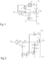
- FIG. 1 illustrates an exemplary embodiment of a gate driver circuit.
- the circuit comprises a gate driver 10, a MOSFET T 0 , and a protection circuit.
- the MOSFET T 0 has a gate electrode G, a drain electrode D, and a source electrode S.
- a load (not shown in Fig. 1 ) may be coupled between the source electrode S and and a reference potential Vss (e.g. ground).
- the reference potential Vss may be ground (in case of a low side switch) or a floating potential (in case of a high side switch).
- the load may be connected between the drain electrode D and a supply potential V DD .
- the MOSFET To may be employed as a low-side switch or a high-side switch of a half-bridge, e.g. in a three-phase bridge circuit (so-called six-pack) or a buck converter.
- the MOSFET T 0 may be implemented as a SiC-MOSFET. Compared to conventional MOSFETs or IGBTs, SiC-MOSFETs usually exhibit excellent switching performance with much lower conduction and switching losses in all temperature ranges. SiC-MOSFETs also have a very low on-state resistance and a low input resistance. The embodiments described herein may, however, also be used for other types of switches.
- the gate driver 10 is configured to receive an input signal S ON and to generate an output voltage V OUT in accordance with the input signal S ON , which usually is a binary signal having only two valid signal levels (i.e. a high level and a low level such as 5V and 0V).
- the gate driver 10 is coupled to the gate electrode G of the MOSFET via a resistor R G that is usually referred to as gate resistor.
- the gate driver 10 is thus able to apply a gate voltage V G to the gate electrode G, which has a voltage level approximately equal to the output voltage V OUT (V G ⁇ V OUT ).
- the first voltage level of the gate voltage V G is chosen high enough to be able to drive the MOSFET T 0 into a highly conductive state (low on-resistance R ON ) when applied at the gate electrode G.
- the first voltage V OUT may be around 15 V.
- the voltage level of the gate voltage VG may be around 11 V during switch-on and around 15V when the MOSFET is switched on. The gate driver 10 is thus able to switch the MOSFET T 0 on and off depending on the input signal S ON .
- the protection circuit includes a comparator circuit 12, an AND-gate 11, an electronic switch 13, and a constant voltage source Q 1 (providing voltage V X ).
- the constant voltage source Qi may be implemented by a series of diodes or Zener diodes.
- the comparator circuit 12 is coupled to the drain electrode D of the MOSFET To and to a control input of switch 13 (via AND-gate 11).
- the switch 13 is coupled between the gate electrode G of the MOSFET To and the constant voltage source Q 1 , so that the voltage V X is applied, as gate voltage V G (V G ⁇ V X ), between the gate electrode G and the source electrode S of the transistor To when the electronic switch 13 is closed.
- the voltage V X generated by voltage source Q 1 is lower than the output voltage V OUT of the gate driver 10 (V X ⁇ V OUT ).
- the second voltage V X may be equal to 11 V while V OUT is 15 V.
- the switch 13 is configured to switch between an on-state and an off-state. In a normal state of the gate driver circuit (steady state after switch-on of transistor T 0 ), the switch 13 is off.
- the comparator circuit 12 is configured to detect whether a drain-source voltage V DS across the drain-source current path of the MOSFET T 0 exceeds a predetermined threshold voltage V TH .
- the comparator circuit 12 When the drain-source voltage V DS exceeds the threshold voltage V TH , the comparator circuit 12 outputs a signal (via AND gate 11) to the switch 13 for it to switch on.
- the AND-gate 11 ensures that the switch 13 can only be switched on by the comparator circuit 12 when the gate driver 10 receives an input signal S ON indicating a switch-on for the MOSFET T 0 . Otherwise, the output signal of the comparator 12 would be blanked.
- the MOSFET T 0 When the input signal S ON received by the gate driver 10 indicates a switch-off, the MOSFET T 0 is switched off and the switch 13 is also switched off (or prevented from switching on).
- the gate driver 10 When the input signal S ON received by the gate driver 10 indicates a switch-on, the gate driver 10 generates a corresponding output voltage V OUT with a sufficiently high voltage level (e.g. 15V), which his applied (via gate resistor R G ) as gate voltage V G to the gate electrode G of the MOSFET T 0 .
- the voltage applied at the gate electrode G is approximately equal to the output voltage V OUT of the gate driver 10 once the gate capacitance is fully charged and the gate current passing through the resistance R G has dropped to zero.
- the MOSFET T 0 is then switched on and the drain-source voltage V DS present between the source electrode S and the drain electrode D drops to comparably low values R ON ⁇ I L , e.g. 100mV or less, which are lower than the above-mentioned threshold value V TH .
- the comparator circuit 12 detects such an excess drain-source voltage V DS greater than the threshold value V TH and generates a respective comparator output signal, which is supplied to the control input of switch 13 for it to switch on.
- the switch 13 When switching on, the switch 13 clamps the gate electrode G of the MOSFET T 0 to the voltage V X of the constant gate source Q 1 via a low-ohmic current path (no resistor is present between the gate electrode G and the voltage source Q 1 ), thus reducing the gate voltage V G to the voltage level V X and, as a consequence, the on-resistance R ON of the MOSFET T 0 increases causing the load current I L and the power dissipation to decrease.
- the device may also comprise a back channel contact (back gate) for switching off the MOSFET.
- the drain-source voltage V DS can drop, in steady state, to be as low as approximately 100 mV or less. Since, in this "normal" on-state the drain-source voltage V DS is under the predetermined voltage threshold V TH of the comparator circuit 12, the comparator circuit 12 provides a comparator output signal that keeps the switch 13 off and thus that gate voltage at the higher level determined by the output voltage VOUT of the gate driver. Conduction losses are reduced as compared to the case when the lower gate voltage V X is applied to the gate electrode G.
- the drain-source voltage V DS present across the MOSFET T 0 is determined by the supply voltage (e.g. V DD -V SS ) applied to the MOSFET T 0 causing a power dissipation of (V DD -V SS ) 2 /R ON in the MOSFET T 0 and a corresponding short-circuit energy.
- the load current I L can be around 20 times stronger than the nominal load current flowing through the MOSFET T 0 in normal on-state.
- the mentioned reduction of power dissipation gives other safety mechanisms more time to detect the over-current/short circuit, to react thereupon, and to trigger safety measures such as a safety switch-switch off of MOSFET T 0 by changing the level of the input signal S ON to a low level.
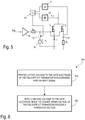
- FIG. 2 illustrates an alternative example of the gate driver circuit according to Figure 1 .
- the switch 13 is implemented as a transistor denoted as transistor T 1 .
- the transistor may be a MOSFET having a comparably low maximum blocking voltage.
- Fig. 2 is directed to an application, in which the MOSFET T 0 is used as a low side switch. Accordingly, the source electrode of the MOSFET T 0 is connected to ground (reference potential V SS ). Similarly, the source electrode of the transistor T 1 is also connected to the ground.
- the transistor T 1 may be implemented as a bipolar transistor.
- the constant voltage source Q 1 is implemented using a Zener diode D1 connected in series with a further diode D 2 , so that the total voltage drop across the series circuit is determined by the sum of the Zener voltage V Z and the forward voltage V D of the further diode D 2 .
- the Zener diode D 1 may have a breakdown voltage V Z of approximately 10V, wherein and the diode D 2 may have a forward voltage V D of about 0.7.
- the series circuit of Zener diode D 1 and the further diode D 2 is coupled between the drain of the transistor T 1 and the gate electrode G of the MOSFET T 0 .
- Zener diode may be implemented by any suitable semiconductor structure that exhibits a behavior substantially corresponding to the behavior of a Zener diode.
- the actual implementation may depend, however, on the technology used for manufacturing the integrated circuit.
- the optional diode D 2 may prevent a short-circuit when the gate driver switches off with a negative voltage.
- the comparator circuit is implemented using a high-voltage diode D 0 , a voltage divider R 1 , R 2 as well as a capacitor C 1 .
- the high-voltage diode D 0 is connected between the drain electrode D of the MOSFET T 0 and the gate electrode G 1 of the transistor T 1 .
- the high-voltage diode D 0 is arranged such that it will be forward biased when the drain-source voltage V DS is lower than the above-mentioned threshold voltage V TH and reverse biased (blocking) when the drain-source voltage V DS exceeds the threshold voltage V TH , which basically depends on the scaling factor provided by the voltage divider as will be explained later with reference to Fig. 3 .
- the function of the diode D 0 is thus to block the high drain-source voltage.
- the voltage divider R 1 , R 2 is connected between an output of the gate driver 10 and ground wherein the middle tap of the voltage divider (circuit node N 1 ) is connected to the gate electrode Gi of the transistor T 1 so that the gate electrode G 1 "sees" the scaled driver output voltage V OUT ⁇ R 2 /(R 1 +R 2 ) when the diode D 0 is blocking.
- the capacitor C 1 is arranged in parallel to the resistance R 2 and is thus connected between the gate electrode G 1 of the transistor T 1 and ground.
- the purpose of the capacitor C 1 basically forms a low pass together with resistors R 1 and R 2 and prevents false activations of the transistor T 1 .
- Fig. 3 is a timing diagram illustrating exemplary waveforms of the drain-source voltage V DS of the MOSFET T 0 , the gate voltage V G at the gate electrode G of the MOSFET T 0 , and the gate voltage V N1 at the gate electrode G 1 of the transistor T 1 in the example gate driver circuit of Fig. 2 when a short-circuit occurs at the load (not shown in Fig. 2 ) at time instant t x .
- a normal on-state of the MOSFET T 0 i.e.
- the drain-source voltage V DS is in the range of a few hundreds of millivolts and basically depends on the load current I L and the (very low) on-resistance R ON of the MOSFET T 0 .
- the diode D 0 pulls the voltage V N1 at circuit node N 1 below approximately 0.8 V.
- the voltage V N1 will be V D +V DS , wherein V D is the forward voltage of diode D 0 (typically 0.6-0.7V) and V DS is, as mentioned, only a few 100 mV.
- the gate G 1 of transistor T 1 is below approximately 0.8 V and thus off (assuming a transistor threshold voltage of above 0.8V for transistor T 1 ).
- the diodes D 1 and D 2 have no effect and the full driver output voltage V OUT (e.g. 15V) is applied as gate voltage V G to the MOSFET T 0 .
- the drain-source voltage V DS of the MOSFET T 0 increases strongly, as shown at time instant t x in the example of Figure 3 .
- the drain-source voltage is so high that the diode D 0 is reverse biased and thus blocking.
- the voltage divider pulls the voltage V N1 applied to the gate of transistor T 1 up to the scaled driver output voltage V OUT ⁇ R 2 /(R 1 +R 2 ) which is high enough to switch on the transistor T 1 .
- the diode D 0 in connection with the voltage divider basically operates as a comparator, wherein the voltage V N1 can be regarded as comparator output voltage.
- the voltage V N1 will be, as explained above, below approximately 0.8 V, whereas for high drain-source voltages V DS (above threshold voltage V DS ), the voltage V N1 will equal V OUT ⁇ R 2 /(R 1 +R 2 ).
- the threshold voltage V TH depends on the characteristics of the transistor T1 and can be slightly below the value V OUT ⁇ R 2 /(R 1 +R 2 ) but higher than the mentioned 0.8 V.
- the gate voltage V G from the driver output voltage V OUT to the reduced voltage V X By reducing the gate voltage V G from the driver output voltage V OUT to the reduced voltage V X , the on-resistance R ON of the MOSFET T 0 is increased and, consequently, the maximum load current I L flowing through the MOSFET T 0 is reduced.
- Fig. 4 illustrates another exemplary implementation of the gate driving circuit of Fig. 1 , wherein the example of Fig. 4 merely distinguishes itself from the gate driver circuit of Fig. 2 by the implementation of the comparator circuit.
- the comparator circuit according to Fig. 4 comprises a comparator 20 instead of diode D 0 .
- the output of comparator 20 is connected to the gate electrode of the transistor T 1 .
- a voltage divider R 3 , R 4 is arranged between the drain electrode of the MOSFET T 0 and ground, wherein the middle tap of the voltage divider R 3 , R 4 is connected to one input of comparator 20, wherein another input of comparator 20 receives a reference voltage V ref .
- the voltage at the middle tap of the voltage divider R 3 , R 4 is denoted as V comp and equals V DS ⁇ R 4 /(R 3 +R 4 ).
- the comparator 20 When the voltage at the first input of the comparator 20 exceeds the reference voltage V ref , the comparator 20 generates an output voltage high enough to switch-on the transistor T 1 .
- the threshold voltage V TH used by the comparator effectively equals to V ref ⁇ (R 3 +R 4 )/R 4 . It is noted that the AND-gate 11 shown in the example of Fig. 1 is not needed in the examples of Figs. 2 and 4 .
- the voltage V X will only be applied to the gate of MOSFET T 0 if the gate driver 10 produces a high-level output voltage.
- the voltage source implemented by the Zener diode D 1 can only provide a voltage V X if the gate driver 10 produces a high-level output voltage V OUT .
- Fig. 5 illustrates another example of the gate driver circuit of Fig. 1 .
- Fig. 5 illustrates an enhancement of the example of Fig. 1 .
- the circuit of Fig. 5 basically differs from the circuit of Fig. 1 in that it the protection circuit includes a second MOSFET T 2 , a second comparator circuit 14 as well as an OR-gate 15, wherein the additional circuit components are used for over-current detection.
- the MOSFET T 2 is arranged in a current mirror configuration with the MOSFET T 0 , which is often referred to as "SenseFET" arrangement.
- a source electrode of the MOSFET T 2 is coupled to the ground via a resistor R S .
- the current I feedback flowing through the MOSFET T 2 thus approximately mirrors the current flowing through the MOSFET T 0 . That is, I feedback ⁇ k ⁇ I L , wherein k denotes a scaling factor lower than one.
- the current I feedback produces a respective voltage drop V feedback across the resistor R S . This voltage drop V feedback is representative of the load current and may be regarded as a load current measurement value.
- the second comparator circuit 14 is coupled to the source electrode of the second MOSFET T 2 to receive the voltage V feedback and has an output coupled to an input of the OR-gate 15.
- the output of comparator 12 is coupled to a second input of the OR-gate 15.
- An output of the OR-gate 15 is coupled to a control input of the switch 13.
- switch 13 is not only switched on when the drain-source voltage V DS increases above a threshold voltage V TH (like in the example of Fig.1 ) but also when the load current i L exceeds an overcurrent threshold.
- the second comparator circuit 14 When the first MOSFET T 0 is subjected to an overcurrent, the feedback current I feedback and thus the voltage V feedback increase strongly.
- the sensed current e.g. the voltage V feedback
- the second comparator circuit 14 exceeds the mentioned overcurrent threshold, then the second comparator circuit 14 outputs a high-level signal to the control input of switch 13 via the OR-gate 15.
- the gate voltage V G of the gate electrode of the first MOSFET T 0 is reduced to the voltage value V X provided by the constant voltage source Q 1 as discussed with reference to Fig. 1 .
- the first comparator circuit 12 outputs a high-level signal to switch 13 via the OR-gate 15.
- the switch 13 is switched on. Both operations may occur in parallel, so that the switch 13 is switched on either when the source-drain voltage V DS of the first MOSFET T 0 exceeds the threshold voltage or when the sense current sensed at the source electrode of the second MOSFET T 2 exceeds the overcurrent threshold. However, the rise in the sensed current may be sensed before the rise in the drain-source voltage.
- the circuit may be configured to switch off the MOSFET when an overcurrent is detected.
- the circuit according to Figure 5 provides two concurrent methods for sensing overcurrents due to a faulty operation of the MOSFET T 0 , thus increasing the safety of the system by means of redundancy. Further circuits comprising the gate driver circuit of Figure 1 are also conceivable.
- the circuit may comprise a shunt resistor connected to the drain of the MOSFET for sensing the load current, or other known current sense circuits.
- Figure 6 is a flowchart illustrating an example method for driving a field-effect transistor to increase the maximum allowable short-circuit time.
- the example method 500 can be employed to operate devices illustrated in this disclosure, such as the gate driving circuits according to Figures 1, 2 , 4 , and 5 .
- Method 500 includes providing a first voltage to the gate electrode G of the field-effect transistor T 0 in accordance with an input signal S ON .
- gate driver 10 can output an output voltage V OUT based on an input signal S ON , so that the first voltage is applied at the gate electrode G of the field-effect transistor T 0 that is sufficient to switch on the field-effect transistor T 0 with a low on-resistance R ON .
- Method 500 further includes applying a second voltage V X as gate voltage V G to the gate electrode G when the source-drain voltage V DS of the field-effect transistor T 0 exceeds a threshold voltage.
- a comparator circuit 12 can receive the drain-source voltage V DS of the field-effect transistor T 0 and compare it to a threshold voltage. The comparator circuit 12 can then output a control signal to the switch 13 so that it switches on when the drain-source voltage V DS exceeds the threshold voltage.
- Method 500 can also include replicating a current I L flowing through the field-effect transistor T 0 .
- a sense field-effect transistor T 2 arranged in a mirror configuration with the field-effect transistor T 0 can output a replicated current I feedback as a proportional mirror current of the current I L .
- Method 500 can further include sensing the replicated current I feedback .
- a comparator circuit 14 can receive a sense current derived from the replicated current I feedback .
- Method 500 may also include applying the second voltage V X to the gate electrode G of the field-effect transistor T 0 when a sense current sensed at the source electrode of the sense field-effect transistor T 2 exceeds a threshold current.
- the comparator circuit 14 can compare the sense current to a threshold current and output a switch-on signal to the switch 13 when the sense current exceeds the threshold current.
Landscapes
- Electronic Switches (AREA)
Abstract
A gate driver circuit is described that comprises a field-effect transistor having a gate electrode, a drain electrode, and a source electrode; a gate driver configured to provide a first voltage to the gate electrode of the field-effect transistor in accordance with an input signal; and a protection circuit coupled to the drain electrode and to the gate electrode and configured to apply a second voltage to the gate electrode when a source-drain voltage of the field-effect transistor exceeds a threshold voltage.
Description
- This application relates to the field of power semiconductor circuits and modules.
- Power transistors are key components in power electronics. They are usually controlled by so-called gate driver circuits, which are configured to switch them on and off. However, in particular during short-circuits or during switch-on, the transistors can be subjected to overcurrents that can cause damage to the transistors. In current and future chip technologies, it may be important to reduce the maximum short-circuit time allowed in order to avoid such damages as much as possible and thus to efficiently protect the device. This is usually done by using an external desaturation detection circuit or an overcurrent detection circuit capable of sensing the output current of the transistor and comparing it to a threshold value. While these methods are well adapted to limiting short circuit times in insulated gate bipolar transistors (IGBT), they may be too slow for protecting silicon carbide metal-oxide-semiconductor field-effect transistors (SiC MOSFETs) at least in some applications. The peak of the short-circuit currents for SiC MOSFETs is indeed much higher than for IGBTs since SiC MOSFETs usually have a much lower resistance. Consequently, damages may occur even during very short short-circuit times. It may be thus very important to quickly reduce the magnitude of the short-circuit currents in order to protect SiC MOSFETs efficiently.
- A first approach to this problem would be to durably reduce the gate voltage of the SiC MOSFET or to use a comparably high-impedance gate resistance. These solutions have the disadvantage of increasing conduction and switching losses. In addition, there may be short-circuits cases in which a high-impedance gate resistance is not a desired option.
- The problem to be solved may be seen in how to provide a gate driver circuit comprising a SiC-MOSFET which is capable of efficiently protecting the SiC-MOSFET from overcurrents in all short-circuit cases, that is during switch-on or when the device is already switched on.
- The above mentioned problem is solved by arranging an additional circuit between the gate driver and the MOSFET that reduces the voltage applied to the gate electrode of the MOSFET during the switch-on of the MOSFET or when a short-circuit is detected. The short-circuit current can be controlled by the gate voltage of the MOSFET. This makes it possible to reduce short-circuit currents. The underlying idea of this solution is to only reduce the gate voltage of the MOSFET in overcurrent situations and to restore the gate voltage to a normal value in the normal on-state of the MOSFET, thus preventing conduction losses in the normal on-state.
- In one example, the disclosure is directed to a gate driver circuit comprising a field-effect transistor having a gate electrode, a drain electrode, and a source electrode; a gate driver configured to provide a first voltage to the gate electrode of the field-effect transistor in accordance with an input signal; and a protection circuit coupled to the drain electrode and to the gate electrode and configured to apply a second voltage to the gate electrode when a source-drain voltage of the field-effect transistor exceeds a threshold voltage.
- In one example, the disclosure is directed to a method for driving a gate of a field-effect transistor comprising the steps of: providing a first voltage to the gate electrode of the field-effect transistor in accordance with an input signal; and applying a second voltage to the gate electrode when the source-drain voltage of the field-effect transistor exceeds a threshold voltage.
- The embodiments described herein can be better understood with reference to the following description and drawings. The components in the figures are not necessarily to scale, emphasis instead being placed upon illustrating the principles of the embodiments. Furthermore, in the figures, like reference numerals designate corresponding parts. In the drawings:
-
Figure 1 is a schematic diagram illustrating an example gate driver circuit, in accordance with one or more techniques described in this disclosure. -
Figure 2 is a schematic diagram illustrating an alternative example gate driver circuit, in accordance with one or more techniques described in this disclosure. -
Figure 3 is a timing diagram illustrating the behavior of several voltages in the example gate driver circuit ofFigure 2 , in accordance with one or more techniques described in this disclosure. -
Figure 4 is a schematic diagram illustrating an alternative example gate driver circuit, in accordance with one or more techniques described in this disclosure. -
Figure 5 is a flowchart illustrating an example method for driving a field-effect transistor, in accordance with one or more techniques described in this disclosure. -
Figure 1 illustrates an exemplary embodiment of a gate driver circuit. Accordingly, the circuit comprises agate driver 10, a MOSFET T0, and a protection circuit. The MOSFET T0 has a gate electrode G, a drain electrode D, and a source electrode S. A load (not shown inFig. 1 ) may be coupled between the source electrode S and and a reference potential Vss (e.g. ground). The reference potential Vss may be ground (in case of a low side switch) or a floating potential (in case of a high side switch). Alternatively, the load may be connected between the drain electrode D and a supply potential VDD. When the transistor T0 is switched on, a load current IL flows from the source electrode S to ground while passing through the load. In some applications, the MOSFET To may be employed as a low-side switch or a high-side switch of a half-bridge, e.g. in a three-phase bridge circuit (so-called six-pack) or a buck converter. The MOSFET T0 may be implemented as a SiC-MOSFET. Compared to conventional MOSFETs or IGBTs, SiC-MOSFETs usually exhibit excellent switching performance with much lower conduction and switching losses in all temperature ranges. SiC-MOSFETs also have a very low on-state resistance and a low input resistance. The embodiments described herein may, however, also be used for other types of switches. - The
gate driver 10 is configured to receive an input signal SON and to generate an output voltage VOUT in accordance with the input signal SON, which usually is a binary signal having only two valid signal levels (i.e. a high level and a low level such as 5V and 0V). Thegate driver 10 is coupled to the gate electrode G of the MOSFET via a resistor RG that is usually referred to as gate resistor. Thegate driver 10 is thus able to apply a gate voltage VG to the gate electrode G, which has a voltage level approximately equal to the output voltage VOUT (VG ≈ VOUT). The first voltage level of the gate voltage VG is chosen high enough to be able to drive the MOSFET T0 into a highly conductive state (low on-resistance RON) when applied at the gate electrode G. For example, the first voltage VOUT may be around 15 V. The voltage level of the gate voltage VG may be around 11 V during switch-on and around 15V when the MOSFET is switched on. Thegate driver 10 is thus able to switch the MOSFET T0 on and off depending on the input signal SON. - In accordance to the depicted example, the protection circuit includes a
comparator circuit 12, anAND-gate 11, anelectronic switch 13, and a constant voltage source Q1 (providing voltage VX). The constant voltage source Qi may be implemented by a series of diodes or Zener diodes. Thecomparator circuit 12 is coupled to the drain electrode D of the MOSFET To and to a control input of switch 13 (via AND-gate 11). Theswitch 13 is coupled between the gate electrode G of the MOSFET To and the constant voltage source Q1, so that the voltage VX is applied, as gate voltage VG (VG ≈ VX), between the gate electrode G and the source electrode S of the transistor To when theelectronic switch 13 is closed. Thereby, the voltage VX generated by voltage source Q1 is lower than the output voltage VOUT of the gate driver 10 (VX<VOUT). For example, the second voltage VX may be equal to 11 V while VOUT is 15 V. - The
switch 13 is configured to switch between an on-state and an off-state. In a normal state of the gate driver circuit (steady state after switch-on of transistor T0), theswitch 13 is off. Thecomparator circuit 12 is configured to detect whether a drain-source voltage VDS across the drain-source current path of the MOSFET T0 exceeds a predetermined threshold voltage VTH. The predetermined threshold voltage VTH may be chosen so that it is higher than the drain-source voltage VDS of the MOSFET T0 in a normal on-state thereof (i.e. when VDS=IL·RON). When the drain-source voltage VDS exceeds the threshold voltage VTH, thecomparator circuit 12 outputs a signal (via AND gate 11) to theswitch 13 for it to switch on. The AND-gate 11 ensures that theswitch 13 can only be switched on by thecomparator circuit 12 when thegate driver 10 receives an input signal SON indicating a switch-on for the MOSFET T0. Otherwise, the output signal of thecomparator 12 would be blanked. - When the input signal SON received by the
gate driver 10 indicates a switch-off, the MOSFET T0 is switched off and theswitch 13 is also switched off (or prevented from switching on). When the input signal SON received by thegate driver 10 indicates a switch-on, thegate driver 10 generates a corresponding output voltage VOUT with a sufficiently high voltage level (e.g. 15V), which his applied (via gate resistor RG) as gate voltage VG to the gate electrode G of the MOSFET T0. As mentioned, the voltage applied at the gate electrode G is approximately equal to the output voltage VOUT of thegate driver 10 once the gate capacitance is fully charged and the gate current passing through the resistance RG has dropped to zero. The MOSFET T0 is then switched on and the drain-source voltage VDS present between the source electrode S and the drain electrode D drops to comparably low values RON·IL, e.g. 100mV or less, which are lower than the above-mentioned threshold value VTH. - Dependent on the load, during the transient switching-on phase of the MOSFET T0, very high currents may flow between the drain electrode D and the source electrode S of the MOSFET T0, leading to a drain-source voltage VDS significantly higher than the mentioned threshold value VTH. The
comparator circuit 12 detects such an excess drain-source voltage VDS greater than the threshold value VTH and generates a respective comparator output signal, which is supplied to the control input ofswitch 13 for it to switch on. When switching on, theswitch 13 clamps the gate electrode G of the MOSFET T0 to the voltage VX of the constant gate source Q1 via a low-ohmic current path (no resistor is present between the gate electrode G and the voltage source Q1), thus reducing the gate voltage VG to the voltage level VX and, as a consequence, the on-resistance RON of the MOSFET T0 increases causing the load current IL and the power dissipation to decrease. This way, overcurrents due to the switching-on of the MOSFET T0, which only occur during a comparably short time interval, and damages to the MOSFET T0 can be avoided or at least reduced. The device may also comprise a back channel contact (back gate) for switching off the MOSFET. - As mentioned, when the MOSFET T0 is conductive, the drain-source voltage VDS can drop, in steady state, to be as low as approximately 100 mV or less. Since, in this "normal" on-state the drain-source voltage VDS is under the predetermined voltage threshold VTH of the
comparator circuit 12, thecomparator circuit 12 provides a comparator output signal that keeps theswitch 13 off and thus that gate voltage at the higher level determined by the output voltage VOUT of the gate driver. Conduction losses are reduced as compared to the case when the lower gate voltage VX is applied to the gate electrode G. - During the on-state of the MOSFET T0, it can happen that the load is short-circuited, which leads to an overcurrent flowing through the MOSFET T0. In such a short-circuit state the drain-source voltage VDS present across the MOSFET T0 is determined by the supply voltage (e.g. VDD-VSS) applied to the MOSFET T0 causing a power dissipation of (VDD-VSS)2/RON in the MOSFET T0 and a corresponding short-circuit energy. During short-circuits the load current IL can be around 20 times stronger than the nominal load current flowing through the MOSFET T0 in normal on-state. These high currents are basically limited only by the on-resistance of the MOSFET T0 and can severly damage the MOSFET T0. The increase of the source-drain voltage VDS resulting from a short circuit or an over-current can be detected by the
comparator circuit 12. When the source-drain voltage VDS exceeds the predetermined threshold voltage VTH due to a short-circuit or an over-current, the same protection mechanism is triggered as in the case of a switching-on of the MOSFET T0. Thecomparator circuit 12 outputs a signal to the switch 13 (via AND gate 11) for it to switch on, thus reducing the gate voltage VG of the MOSFET T0 to the lower voltage level VX. As a consequence, the on-resistance RON of the MOSFET T0 is increased and, consequently, the power dissipation is reduced. - The mentioned reduction of power dissipation gives other safety mechanisms more time to detect the over-current/short circuit, to react thereupon, and to trigger safety measures such as a safety switch-switch off of MOSFET T0 by changing the level of the input signal SON to a low level.
-
Figure 2 illustrates an alternative example of the gate driver circuit according toFigure 1 . In the depicted example, theswitch 13 is implemented as a transistor denoted as transistor T1. The transistor may be a MOSFET having a comparably low maximum blocking voltage.Fig. 2 is directed to an application, in which the MOSFET T0 is used as a low side switch. Accordingly, the source electrode of the MOSFET T0 is connected to ground (reference potential VSS). Similarly, the source electrode of the transistor T1 is also connected to the ground. As an alternative, the transistor T1 may be implemented as a bipolar transistor. - In the example of
Fig. 2 , the constant voltage source Q1 is implemented using a Zener diode D1 connected in series with a further diode D2, so that the total voltage drop across the series circuit is determined by the sum of the Zener voltage VZ and the forward voltage VD of the further diode D2. For example, the Zener diode D1 may have a breakdown voltage VZ of approximately 10V, wherein and the diode D2 may have a forward voltage VD of about 0.7. Thus, the voltage VX can be calculated as VX=VZ+VD. The series circuit of Zener diode D1 and the further diode D2 is coupled between the drain of the transistor T1 and the gate electrode G of the MOSFET T0. It is understood that the Zener diode may be implemented by any suitable semiconductor structure that exhibits a behavior substantially corresponding to the behavior of a Zener diode. The actual implementation may depend, however, on the technology used for manufacturing the integrated circuit. The optional diode D2 may prevent a short-circuit when the gate driver switches off with a negative voltage. - In the example of
Fig. 2 , the comparator circuit is implemented using a high-voltage diode D0, a voltage divider R1, R2 as well as a capacitor C1. The high-voltage diode D0 is connected between the drain electrode D of the MOSFET T0 and the gate electrode G1 of the transistor T1. The high-voltage diode D0 is arranged such that it will be forward biased when the drain-source voltage VDS is lower than the above-mentioned threshold voltage VTH and reverse biased (blocking) when the drain-source voltage VDS exceeds the threshold voltage VTH, which basically depends on the scaling factor provided by the voltage divider as will be explained later with reference toFig. 3 . The function of the diode D0 is thus to block the high drain-source voltage. The voltage divider R1, R2 is connected between an output of thegate driver 10 and ground wherein the middle tap of the voltage divider (circuit node N1) is connected to the gate electrode Gi of the transistor T1 so that the gate electrode G1 "sees" the scaled driver output voltage VOUT·R2/(R1+R2) when the diode D0 is blocking. The capacitor C1 is arranged in parallel to the resistance R2 and is thus connected between the gate electrode G1 of the transistor T1 and ground. The purpose of the capacitor C1 basically forms a low pass together with resistors R1 and R2 and prevents false activations of the transistor T1. - The functioning of the gate driver circuit according to
Fig. 2 will now be explained with the help of the timing diagrams included inFig. 3. Fig. 3 is a timing diagram illustrating exemplary waveforms of the drain-source voltage VDS of the MOSFET T0, the gate voltage VG at the gate electrode G of the MOSFET T0, and the gate voltage VN1 at the gate electrode G1 of the transistor T1 in the example gate driver circuit ofFig. 2 when a short-circuit occurs at the load (not shown inFig. 2 ) at time instant tx. In a normal on-state of the MOSFET T0 (i.e. for times t<tx, before the short circuit occurs), the drain-source voltage VDS is in the range of a few hundreds of millivolts and basically depends on the load current IL and the (very low) on-resistance RON of the MOSFET T0. - Without a short-circuit (i.e. for times t<tx in
Fig. 3 ), the diode D0 pulls the voltage VN1 at circuit node N1 below approximately 0.8 V. In this situation the voltage VN1 will be VD+VDS, wherein VD is the forward voltage of diode D0 (typically 0.6-0.7V) and VDS is, as mentioned, only a few 100 mV. As a consequence, the gate G1 of transistor T1 is below approximately 0.8 V and thus off (assuming a transistor threshold voltage of above 0.8V for transistor T1). In this situation (transistor T1 off), the diodes D1 and D2 have no effect and the full driver output voltage VOUT (e.g. 15V) is applied as gate voltage VG to the MOSFET T0. - During a short-circuit or in an over-current situation, the drain-source voltage VDS of the MOSFET T0 increases strongly, as shown at time instant tx in the example of
Figure 3 . After the time instant tx (i.e. for times t<tx) the drain-source voltage is so high that the diode D0 is reverse biased and thus blocking. As a consequence, the voltage divider pulls the voltage VN1 applied to the gate of transistor T1 up to the scaled driver output voltage VOUT·R2/(R1+R2) which is high enough to switch on the transistor T1. Accordingly, the diode D0 in connection with the voltage divider basically operates as a comparator, wherein the voltage VN1 can be regarded as comparator output voltage. For low drain-source voltages VDS, the voltage VN1 will be, as explained above, below approximately 0.8 V, whereas for high drain-source voltages VDS (above threshold voltage VDS), the voltage VN1 will equal VOUT·R2/(R1+R2). The threshold voltage VTH depends on the characteristics of the transistor T1 and can be slightly below the value VOUT·R2/(R1+R2) but higher than the mentioned 0.8 V. The increase of the gate voltage VN1 from approximately 0.8 V to VOUT·R2/(R1+R2), e.g. 3V, triggers a switch-on of the transistor T1, thus applying a lower gate voltage VX to the gate of the MOSFET T0, which is - in the example ofFig. 2 - dependent on the Zener voltage of diode D1. By reducing the gate voltage VG from the driver output voltage VOUT to the reduced voltage VX, the on-resistance RON of the MOSFET T0 is increased and, consequently, the maximum load current IL flowing through the MOSFET T0 is reduced. As mentioned reducing the maximum load current in short-circuit situations gives external safety mechanisms more time to initiate an emergency switch-off of the MOSFET T0. In other words, the maximum allowable short-circuit time is increased. A higher maximum short-circuit time also helps to avoid "false alarms", i.e. undesired emergency switch-off of the MOSFET T0 in case a short-circuit is wrongly detected by the mentioned safety mechanism. -
Fig. 4 illustrates another exemplary implementation of the gate driving circuit ofFig. 1 , wherein the example ofFig. 4 merely distinguishes itself from the gate driver circuit ofFig. 2 by the implementation of the comparator circuit. Accordingly, the comparator circuit according toFig. 4 comprises acomparator 20 instead of diode D0. The output ofcomparator 20 is connected to the gate electrode of the transistor T1. A voltage divider R3, R4 is arranged between the drain electrode of the MOSFET T0 and ground, wherein the middle tap of the voltage divider R3, R4 is connected to one input ofcomparator 20, wherein another input ofcomparator 20 receives a reference voltage Vref. The voltage at the middle tap of the voltage divider R3, R4 is denoted as Vcomp and equals VDS·R4/(R3+R4). - When the voltage at the first input of the
comparator 20 exceeds the reference voltage Vref, thecomparator 20 generates an output voltage high enough to switch-on the transistor T1. Similarly to the previous examples, as a result, the gate electrode G of the MOSFET T0 is clamped to the voltage VX = VZ + VD of the constant voltage source formed by the Zener diode D1 and the diode D2. The threshold voltage VTH used by the comparator effectively equals to Vref·(R3+R4)/R4. It is noted that the AND-gate 11 shown in the example ofFig. 1 is not needed in the examples ofFigs. 2 and4 . The AND-operation is implicitly achieved as in these examples the voltage VX will only be applied to the gate of MOSFET T0 if thegate driver 10 produces a high-level output voltage. In other words, the voltage source implemented by the Zener diode D1 can only provide a voltage VX if thegate driver 10 produces a high-level output voltage VOUT. -
Fig. 5 illustrates another example of the gate driver circuit ofFig. 1 . Basically,Fig. 5 illustrates an enhancement of the example ofFig. 1 . Accordingly, the circuit ofFig. 5 basically differs from the circuit ofFig. 1 in that it the protection circuit includes a second MOSFET T2, asecond comparator circuit 14 as well as an OR-gate 15, wherein the additional circuit components are used for over-current detection. - The MOSFET T2 is arranged in a current mirror configuration with the MOSFET T0, which is often referred to as "SenseFET" arrangement. In the present example, this means that the drain electrodes of both MOSFETs T0, T2 are connected to each other and that the gate electrodes of both MOSFETs T0, T2 are connected to each other. A source electrode of the MOSFET T2 is coupled to the ground via a resistor RS. The current Ifeedback flowing through the MOSFET T2 thus approximately mirrors the current flowing through the MOSFET T0. That is, Ifeedback≈k·IL, wherein k denotes a scaling factor lower than one. The current Ifeedback produces a respective voltage drop Vfeedback across the resistor RS. This voltage drop Vfeedback is representative of the load current and may be regarded as a load current measurement value.
- The
second comparator circuit 14 is coupled to the source electrode of the second MOSFET T2 to receive the voltage Vfeedback and has an output coupled to an input of the OR-gate 15. The output ofcomparator 12 is coupled to a second input of the OR-gate 15. An output of the OR-gate 15 is coupled to a control input of theswitch 13. As compared to the example ofFig. 1 , the present example ofFig. 5 allows the evaluation of a further condition to switch on theswitch 13. Accordingly, switch 13 is not only switched on when the drain-source voltage VDS increases above a threshold voltage VTH (like in the example ofFig.1 ) but also when the load current iL exceeds an overcurrent threshold. - When the first MOSFET T0 is subjected to an overcurrent, the feedback current Ifeedback and thus the voltage Vfeedback increase strongly. When the sensed current (e.g. the voltage Vfeedback) exceeds the mentioned overcurrent threshold, then the
second comparator circuit 14 outputs a high-level signal to the control input ofswitch 13 via the OR-gate 15. As a consequence, the gate voltage VG of the gate electrode of the first MOSFET T0 is reduced to the voltage value VX provided by the constant voltage source Q1 as discussed with reference toFig. 1 . Similarly, when the drain-source voltage VDS of the first MOSFET T0 exceeds the threshold voltage, thefirst comparator circuit 12 outputs a high-level signal to switch 13 via the OR-gate 15. Again, as a result, theswitch 13 is switched on. Both operations may occur in parallel, so that theswitch 13 is switched on either when the source-drain voltage VDS of the first MOSFET T0 exceeds the threshold voltage or when the sense current sensed at the source electrode of the second MOSFET T2 exceeds the overcurrent threshold. However, the rise in the sensed current may be sensed before the rise in the drain-source voltage. The circuit may be configured to switch off the MOSFET when an overcurrent is detected. The circuit according toFigure 5 provides two concurrent methods for sensing overcurrents due to a faulty operation of the MOSFET T0, thus increasing the safety of the system by means of redundancy. Further circuits comprising the gate driver circuit ofFigure 1 are also conceivable. The circuit may comprise a shunt resistor connected to the drain of the MOSFET for sensing the load current, or other known current sense circuits. -
Figure 6 is a flowchart illustrating an example method for driving a field-effect transistor to increase the maximum allowable short-circuit time. Theexample method 500 can be employed to operate devices illustrated in this disclosure, such as the gate driving circuits according toFigures 1, 2 ,4 , and5 . -
Method 500 includes providing a first voltage to the gate electrode G of the field-effect transistor T0 in accordance with an input signal SON. For example,gate driver 10 can output an output voltage VOUT based on an input signal SON, so that the first voltage is applied at the gate electrode G of the field-effect transistor T0 that is sufficient to switch on the field-effect transistor T0 with a low on-resistance RON. -
Method 500 further includes applying a second voltage VX as gate voltage VG to the gate electrode G when the source-drain voltage VDS of the field-effect transistor T0 exceeds a threshold voltage. For example, acomparator circuit 12 can receive the drain-source voltage VDS of the field-effect transistor T0 and compare it to a threshold voltage. Thecomparator circuit 12 can then output a control signal to theswitch 13 so that it switches on when the drain-source voltage VDS exceeds the threshold voltage. -
Method 500 can also include replicating a current IL flowing through the field-effect transistor T0. For example, a sense field-effect transistor T2 arranged in a mirror configuration with the field-effect transistor T0 can output a replicated current Ifeedback as a proportional mirror current of the current IL. Method 500 can further include sensing the replicated current Ifeedback. For example, acomparator circuit 14 can receive a sense current derived from the replicated current Ifeedback. Method 500 may also include applying the second voltage VX to the gate electrode G of the field-effect transistor T0 when a sense current sensed at the source electrode of the sense field-effect transistor T2 exceeds a threshold current. For example, thecomparator circuit 14 can compare the sense current to a threshold current and output a switch-on signal to theswitch 13 when the sense current exceeds the threshold current. - Although various embodiments have been illustrated and described with respect to one or more specific implementations, alterations and/or modifications may be made to the illustrated examples without departing from the spirit and scope of the features and structures recited herein. With particular regard to the various functions performed by the above described components or structures (units, assemblies, devices, circuits, systems, etc.), the terms (including a reference to a "means") used to describe such components are intended to correspond - unless otherwise indicated - to any component or structure that performs the specified function of the described component (e.g., that is functionally equivalent), even if it is not structurally equivalent to the disclosed structure that performs the function in the herein illustrated exemplary implementations of the present disclosure.
Claims (12)
- A gate driver circuit comprising:a field-effect transistor (T0) having a gate electrode (G), a drain electrode (D), and a source electrode (S);a gate driver (10) configured to provide a first voltage (VOUT) as gate voltage (VG) to the gate electrode (G) of the field-effect transistor (T0) in accordance with an input signal (SON); anda protection circuit coupled to the drain electrode (D) and to the gate electrode (G) and configured to apply a second voltage (VX) to the gate electrode (G) when a drain-source voltage (VDS) of the field-effect transistor (T0) exceeds a threshold voltage (VTH).
- The gate driver circuit according to claim 1, wherein the protection circuit comprises:a switch coupled to the gate electrode and configured to switch between an on-state and an off-state;a comparator circuit coupled to the drain electrode and to the switch and configured to receive the drain-source voltage and to control the switch so that it switches on the switch when the drain-source voltage exceeds a threshold voltage; anda constant voltage source coupled to the switch and configured to provide the second voltage.
- The gate driver circuit according to claim 2, wherein the comparator circuit comprises:a high-voltage diode coupled to the drain electrode and to a control electrode of the switch and arranged so that it is passing when the source-drain voltage is lower than the threshold voltage and it is blocking when the source-drain voltage exceeds the threshold voltage; anda voltage divider coupled to an output of the gate driver and to the control electrode of the switch.
- The gate driver circuit according to claim 2, wherein the comparator circuit comprises:a comparator coupled to the drain electrode and to the switch and configured to compare the drain-source voltage to the threshold voltage and generate a switch-on signal for the switch when the drain-source voltage exceeds the threshold voltage; anda voltage divider arranged between the drain electrode and an input of the comparator.
- The gate driver circuit according to one the claims 2 to 4, wherein the switch is a transistor with a low reverse voltage and the comparator circuit is coupled to the gate of the transistor.
- The gate driver circuit according to claim 5, wherein the switch is a bipolar transistor.
- The gate driver circuit according to one the claims 2 to 6, wherein the constant voltage source comprises a Zener diode and a polarity reversal protection diode.
- The gate driver circuit according to one the claims 1 to 7, wherein the field-effect transistor is a SIC-MOS transistor.
- The gate driver circuit according to one the claims 1 to 8, wherein the gate driver circuit further comprises:a sense field-effect transistor arranged in a mirror configuration with the field-effect transistor and configured to replicate a current flowing through the field-effect transistor;the protection circuit configured to apply the second voltage to the gate electrode when the source-drain voltage of the field-effect transistor exceeds the threshold voltage or when a sense current sensed at a source electrode of the sense field-effect transistor exceeds a threshold current.
- Method for driving a gate of a field-effect transistor comprising the steps of:providing a first voltage to the gate electrode of the field-effect transistor in accordance with an input signal;applying a second voltage to the gate electrode when the source-drain voltage of the field-effect transistor exceeds a threshold voltage.
- Method according to claim 10 further comprising the steps of:receiving the drain-source voltagecomparing a source-drain voltage of the field-effect transistor to a threshold voltage; andcontrolling a switch so that it switches on the switch when the drain-source voltage exceeds a threshold voltage.
- Method according to one of the claims 10 or 11, further comprising the steps of:replicating a current flowing through the power field-effect transistor;sensing the replicated current; andapplying the second voltage to the gate electrode when a sense current sensed at a source electrode of the sense field-effect transistor exceeds a threshold current.
Priority Applications (1)
| Application Number | Priority Date | Filing Date | Title |
|---|---|---|---|
| EP19171257.9A EP3731413A1 (en) | 2019-04-26 | 2019-04-26 | Gate driver circuit and method for driving a gate of a field-effect transistor |
Applications Claiming Priority (1)
| Application Number | Priority Date | Filing Date | Title |
|---|---|---|---|
| EP19171257.9A EP3731413A1 (en) | 2019-04-26 | 2019-04-26 | Gate driver circuit and method for driving a gate of a field-effect transistor |
Publications (1)
| Publication Number | Publication Date |
|---|---|
| EP3731413A1 true EP3731413A1 (en) | 2020-10-28 |
Family
ID=66290242
Family Applications (1)
| Application Number | Title | Priority Date | Filing Date |
|---|---|---|---|
| EP19171257.9A Withdrawn EP3731413A1 (en) | 2019-04-26 | 2019-04-26 | Gate driver circuit and method for driving a gate of a field-effect transistor |
Country Status (1)
| Country | Link |
|---|---|
| EP (1) | EP3731413A1 (en) |
Cited By (2)
| Publication number | Priority date | Publication date | Assignee | Title |
|---|---|---|---|---|
| CN112468131A (en) * | 2020-11-30 | 2021-03-09 | 珠海格力电器股份有限公司 | Drive circuit and drive device |
| CN113285699A (en) * | 2021-06-08 | 2021-08-20 | 南京昉芯微电子有限公司 | Novel grid driving circuit |
Citations (2)
| Publication number | Priority date | Publication date | Assignee | Title |
|---|---|---|---|---|
| US5361008A (en) * | 1992-03-03 | 1994-11-01 | Nec Corporation | Switching circuit of low power consumption |
| US5444591A (en) * | 1993-04-01 | 1995-08-22 | International Rectifier Corporation | IGBT fault current limiting circuit |
-
2019
- 2019-04-26 EP EP19171257.9A patent/EP3731413A1/en not_active Withdrawn
Patent Citations (2)
| Publication number | Priority date | Publication date | Assignee | Title |
|---|---|---|---|---|
| US5361008A (en) * | 1992-03-03 | 1994-11-01 | Nec Corporation | Switching circuit of low power consumption |
| US5444591A (en) * | 1993-04-01 | 1995-08-22 | International Rectifier Corporation | IGBT fault current limiting circuit |
Cited By (3)
| Publication number | Priority date | Publication date | Assignee | Title |
|---|---|---|---|---|
| CN112468131A (en) * | 2020-11-30 | 2021-03-09 | 珠海格力电器股份有限公司 | Drive circuit and drive device |
| CN112468131B (en) * | 2020-11-30 | 2023-12-12 | 珠海格力电器股份有限公司 | Drive circuits and drive devices |
| CN113285699A (en) * | 2021-06-08 | 2021-08-20 | 南京昉芯微电子有限公司 | Novel grid driving circuit |
Similar Documents
| Publication | Publication Date | Title |
|---|---|---|
| US11139808B2 (en) | Semiconductor device and power conversion system | |
| EP2763319B1 (en) | Short circuit protection circuit and method for insulated gate bipolar transistor | |
| US10038438B2 (en) | Power semiconductor element driving circuit | |
| EP2736170B1 (en) | Cascoded semiconductor devices | |
| US8670219B2 (en) | High-voltage devices with integrated over-voltage protection and associated methods | |
| US9755630B2 (en) | Solid-state circuit breakers and related circuits | |
| CN101189795B (en) | Power Controllers and Semiconductor Devices | |
| US9595949B2 (en) | Control of a clamp circuit during transient conditions | |
| CN107852159B (en) | drive | |
| JP2016092907A (en) | Semiconductor device | |
| JP2007028747A (en) | Overvoltage protection circuit | |
| CN109327011B (en) | Overvoltage protection device | |
| CN118117999A (en) | Power semiconductor device with voltage clamping circuit | |
| US11056969B2 (en) | Boost converter short circuit protection | |
| CN105990825B (en) | Overvoltage protection device | |
| EP3070830B1 (en) | Rectifier circuit with reduced reverse recovery time | |
| US5488533A (en) | Methods and apparatus for isolating a power network from a load during an overcurrent condition | |
| US12312094B2 (en) | Aircraft solid sate power controller and aircraft electric power supply system | |
| CN120377881A (en) | Intelligent power semiconductor switching device with self-diagnosis function and method thereof | |
| US5576615A (en) | Method and circuit for detecting faulty recirculation diode in a switched mode power supply | |
| KR20230055364A (en) | Apparatus for protecting a short in a switch | |
| WO2024261949A1 (en) | Semiconductor drive device and electric power conversion device | |
| CN119836749A (en) | Short-circuit protection for power switch | |
| US12273098B2 (en) | Method for operating a power transistor circuit | |
| KR20220037852A (en) | Short circuit protection for power switch |
Legal Events
| Date | Code | Title | Description |
|---|---|---|---|
| PUAI | Public reference made under article 153(3) epc to a published international application that has entered the european phase |
Free format text: ORIGINAL CODE: 0009012 |
|
| STAA | Information on the status of an ep patent application or granted ep patent |
Free format text: STATUS: THE APPLICATION HAS BEEN PUBLISHED |
|
| AK | Designated contracting states |
Kind code of ref document: A1 Designated state(s): AL AT BE BG CH CY CZ DE DK EE ES FI FR GB GR HR HU IE IS IT LI LT LU LV MC MK MT NL NO PL PT RO RS SE SI SK SM TR |
|
| AX | Request for extension of the european patent |
Extension state: BA ME |
|
| STAA | Information on the status of an ep patent application or granted ep patent |
Free format text: STATUS: THE APPLICATION IS DEEMED TO BE WITHDRAWN |
|
| 18D | Application deemed to be withdrawn |
Effective date: 20210429 |