EP3731293A1 - Display apparatus - Google Patents
Display apparatus Download PDFInfo
- Publication number
- EP3731293A1 EP3731293A1 EP20165050.4A EP20165050A EP3731293A1 EP 3731293 A1 EP3731293 A1 EP 3731293A1 EP 20165050 A EP20165050 A EP 20165050A EP 3731293 A1 EP3731293 A1 EP 3731293A1
- Authority
- EP
- European Patent Office
- Prior art keywords
- layer
- encapsulation layer
- inorganic encapsulation
- barrier wall
- capping layer
- Prior art date
- Legal status (The legal status is an assumption and is not a legal conclusion. Google has not performed a legal analysis and makes no representation as to the accuracy of the status listed.)
- Granted
Links
Images





Classifications
-
- H—ELECTRICITY
- H10—SEMICONDUCTOR DEVICES; ELECTRIC SOLID-STATE DEVICES NOT OTHERWISE PROVIDED FOR
- H10K—ORGANIC ELECTRIC SOLID-STATE DEVICES
- H10K59/00—Integrated devices, or assemblies of multiple devices, comprising at least one organic light-emitting element covered by group H10K50/00
- H10K59/10—OLED displays
- H10K59/12—Active-matrix OLED [AMOLED] displays
- H10K59/126—Shielding, e.g. light-blocking means over the TFTs
-
- H—ELECTRICITY
- H10—SEMICONDUCTOR DEVICES; ELECTRIC SOLID-STATE DEVICES NOT OTHERWISE PROVIDED FOR
- H10K—ORGANIC ELECTRIC SOLID-STATE DEVICES
- H10K59/00—Integrated devices, or assemblies of multiple devices, comprising at least one organic light-emitting element covered by group H10K50/00
- H10K59/80—Constructional details
- H10K59/87—Passivation; Containers; Encapsulations
- H10K59/873—Encapsulations
- H10K59/8731—Encapsulations multilayered coatings having a repetitive structure, e.g. having multiple organic-inorganic bilayers
-
- H—ELECTRICITY
- H10—SEMICONDUCTOR DEVICES; ELECTRIC SOLID-STATE DEVICES NOT OTHERWISE PROVIDED FOR
- H10K—ORGANIC ELECTRIC SOLID-STATE DEVICES
- H10K50/00—Organic light-emitting devices
- H10K50/80—Constructional details
- H10K50/84—Passivation; Containers; Encapsulations
- H10K50/844—Encapsulations
-
- H—ELECTRICITY
- H10—SEMICONDUCTOR DEVICES; ELECTRIC SOLID-STATE DEVICES NOT OTHERWISE PROVIDED FOR
- H10K—ORGANIC ELECTRIC SOLID-STATE DEVICES
- H10K59/00—Integrated devices, or assemblies of multiple devices, comprising at least one organic light-emitting element covered by group H10K50/00
- H10K59/80—Constructional details
- H10K59/87—Passivation; Containers; Encapsulations
- H10K59/871—Self-supporting sealing arrangements
- H10K59/8723—Vertical spacers, e.g. arranged between the sealing arrangement and the OLED
-
- H—ELECTRICITY
- H10—SEMICONDUCTOR DEVICES; ELECTRIC SOLID-STATE DEVICES NOT OTHERWISE PROVIDED FOR
- H10H—INORGANIC LIGHT-EMITTING SEMICONDUCTOR DEVICES HAVING POTENTIAL BARRIERS
- H10H20/00—Individual inorganic light-emitting semiconductor devices having potential barriers, e.g. light-emitting diodes [LED]
- H10H20/80—Constructional details
- H10H20/84—Coatings, e.g. passivation layers or antireflective coatings
-
- H—ELECTRICITY
- H10—SEMICONDUCTOR DEVICES; ELECTRIC SOLID-STATE DEVICES NOT OTHERWISE PROVIDED FOR
- H10K—ORGANIC ELECTRIC SOLID-STATE DEVICES
- H10K2102/00—Constructional details relating to the organic devices covered by this subclass
-
- H—ELECTRICITY
- H10—SEMICONDUCTOR DEVICES; ELECTRIC SOLID-STATE DEVICES NOT OTHERWISE PROVIDED FOR
- H10K—ORGANIC ELECTRIC SOLID-STATE DEVICES
- H10K59/00—Integrated devices, or assemblies of multiple devices, comprising at least one organic light-emitting element covered by group H10K50/00
- H10K59/10—OLED displays
- H10K59/12—Active-matrix OLED [AMOLED] displays
-
- H—ELECTRICITY
- H10—SEMICONDUCTOR DEVICES; ELECTRIC SOLID-STATE DEVICES NOT OTHERWISE PROVIDED FOR
- H10K—ORGANIC ELECTRIC SOLID-STATE DEVICES
- H10K59/00—Integrated devices, or assemblies of multiple devices, comprising at least one organic light-emitting element covered by group H10K50/00
- H10K59/10—OLED displays
- H10K59/12—Active-matrix OLED [AMOLED] displays
- H10K59/122—Pixel-defining structures or layers, e.g. banks
Definitions
- One or more embodiments relate to an apparatus, and more particularly, to a display apparatus.
- a display apparatus is an apparatus for displaying images and may include a liquid crystal display, an electrophoretic display, an organic light-emitting display, an inorganic light-emitting display, a field emission display, a surface-conduction electron-emitter display, a plasma display, a cathode ray display, etc.
- a display apparatus includes a display area and a non-display area, wherein the display area displays images and the non-display area has wires arranged therein for transferring signals to the display area.
- An aspect of one or more embodiments is directed toward a display apparatus having a thin film encapsulation layer that has increased adherence (e.g., may not be separated) while preventing or protecting from infiltration of external moisture and/or oxygen.
- a display apparatus includes: a substrate including a display area for displaying images and a non-display area adjacent to (e.g., on an outer portion of) the display area; a thin film encapsulation layer including a first inorganic encapsulation layer, an organic encapsulation layer, and a second inorganic encapsulation layer stacked on the substrate; a barrier wall on the non-display area; and a capping layer between the substrate and the thin film encapsulation layer in a first direction, an end of the capping layer being located on an outer portion of the barrier wall.
- the capping layer may include an inorganic material.
- the inorganic material may include at least one selected from SiN x , TiO x , ZrO x and HfO x .
- the end of the capping layer may be closer to the barrier wall than an end of at least one of the first inorganic encapsulation layer and the second inorganic encapsulation layer is to the barrier wall in a second direction perpendicular to the first direction.
- the end of the capping layer may be farther from the barrier wall than an end of at least one of the first inorganic encapsulation layer and the second inorganic encapsulation layer is to the barrier wall in a second direction perpendicular to the first direction.
- the end of the capping layer and an end of at least one of the first inorganic encapsulation layer and the second inorganic encapsulation layer may be identical in location to each other in a second direction perpendicular to the first direction.
- At least one of the end of the capping layer, an end of the first inorganic encapsulation layer and an end of the second inorganic encapsulation layer and an end of the substrate are identical in location to each other in a second direction perpendicular to the first direction.
- the barrier wall may include: a first barrier wall on the non-display area; and a second barrier wall on the non-display area, the second barrier wall being spaced from the first barrier wall.
- the capping layer, the first inorganic encapsulation layer, and the second inorganic encapsulation layer may be sequentially stacked in the first direction on an area between the barrier wall and an end of the substrate in a second direction perpendicular to the first direction.
- the capping layer may have a refractive index of 1.8 or greater.
- a display apparatus includes: a substrate including a display area for displaying images and a non-display area adjuacent to (e.g., on an outer portion of) the display area; a thin film encapsulation layer including a first inorganic encapsulation layer, an organic encapsulation layer, and a second inorganic encapsulation layer stacked in a first direction on the substrate; a barrier wall on the non-display area; a cladding layer on the substrate, the cladding layer being spaced from the barrier wall towards an end of the substrate in a second direction perpendicular to the first direction; and a capping layer between the substrate and the thin film encapsulation layer in the first direction, the capping layer being at least partially located between the barrier wall and the cladding layer in the second direction.
- the capping layer may include an inorganic material.
- the inorganic material may include at least one selected from SiN x , TiO x , ZrOx, and HfOx.
- An end of the capping layer may be between the barrier wall and the cladding layer in the second direction.
- An end of the capping layer and an end of the substrate are identical in location to each other in the second direction.
- An end of the capping layer may be at a location different from an end of at least one of the first inorganic encapsulation layer and the second inorganic encapsulation layer in the second direction, or the end of the capping layer may be at a same location as the end of at least one of the first inorganic encapsulation layer and the second inorganic encapsulation layer in the second direction.
- the capping layer, the first inorganic encapsulation layer, and the second inorganic encapsulation layer may be sequentially stacked in the first direction on an area between the barrier wall and an end of the substrate in the second direction.
- a display apparatus includes: a substrate including a display area for displaying images and a non-display area adjacent to (e.g., on an outer portion of) the display area; a thin film encapsulation layer including a first inorganic encapsulation layer, an organic encapsulation layer, and a second inorganic encapsulation layer stacked on the substrate; a barrier wall on the non-display area; and a capping layer between the substrate and the thin film encapsulation layer, the capping layer covering a front surface of the barrier wall, and the capping layer including an inorganic material.
- a density of the capping layer may be greater than a density of at least one of the first inorganic encapsulation layer and the second inorganic encapsulation layer.
- the capping layer may have a thickness of 1000 ⁇ or less.
- the X-axis, the Y-axis, and the Z-axis are not limited to three axes of the rectangular coordinate system, and may be interpreted in a broader sense.
- the X-axis, the Y-axis, and the Z-axis may be perpendicular to one another, or may represent different directions that are not perpendicular to one another.
- a specific process order may be performed differently from the described order.
- two consecutively described processes may be performed substantially at the same time or performed in an order opposite to the described order.
- FIG. 1 is a plan view of a display apparatus according to an embodiment.
- FIG. 2 is a cross-sectional view taken along a line II-II' of FIG. 1 .
- FIG. 3 is a cross-sectional view showing a relationship between the display apparatus of FIG. 2 and a mask used in manufacturing the display apparatus.
- the display apparatus 1000 includes a substrate 100.
- the substrate 100 includes a display area DA and a non-display area PA adjacent to the display area DA.
- a plurality of pixels are arranged in the display area DA of the substrate 100 to display images.
- Various display devices such as an organic light-emitting device (OLED), a thin film transistor, a capacitor, etc.
- OLED organic light-emitting device
- a thin film transistor thin film transistor
- a capacitor etc.
- a driving current flowing through the display devices is generated according to a gate signal, a data signal, a driving voltage (ELVDD), a common voltage (ELVSS), etc., supplied to the pixel, and the display device may emit light having a luminance corresponding to the driving current.
- the non-display area PA is adjacent to the display area DA.
- a wiring portion 600 for supplying various signals and/or power source applied to the display area DA may be arranged in the non-display area PA.
- the wiring portion 600 may include a drive circuit.
- the drive circuit may include at least one selected from a scan driving circuit, a terminal portion, a driving power supply line, and a second line 210, and may further include a thin film transistor T3 for controlling electrical signals applied to the display area DA.
- a barrier wall or a trench may be arranged in the non-display area PA, and the barrier wall or the trench may block a flow of an organic layer that is used to manufacture the display apparatus 1000.
- At least one selected from the scan driving circuit, the terminal portion, the driving power supply line, the second line 210, and the thin film transistor T3 may be arranged in the non-display area PA at a longer side of the display apparatus 1000 (e.g., the longer side being parallel to the Y-axis) or the non-display area PA at a shorter side of the display apparatus 1000 (e.g., the shorter side being parallel to the X-axis).
- the display apparatus 1000 includes the substrate 100 including the display area DA and the non-display area PA, and a thin film encapsulation layer 500 for encapsulating the display area DA and the non-display area PA.
- the substrate 100 may include various materials.
- the substrate 100 may include a transparent glass material containing SiO 2 as a main component.
- the substrate 100 is not limited thereto, that is, it may include a transparent plastic material.
- the plastic material may include an insulating organic material, that is, an organic material selected from the group consisting of a polyether sulfone, polyacrylate, polyetherimide, polyethylene naphthalate, polyethylene terephthalate, polyphenylene sulfide, polyarylate, polyimide, polycarbonate, cellulose triacetate, cellulose acetate propionate, etc.
- the substrate 100 may have a multi-layered structure including a layer including the plastic material and an inorganic layer.
- a buffer layer 101 is located on the substrate 100 to reduce or block infiltration of impurities, moisture, or external air from a lower portion of the substrate 100, and to provide a flat surface on the substrate 100.
- the buffer layer 101 may include an inorganic material (such as an oxide material and/or a nitride material), an organic material, or an inorganic-organic composite material, and may have a single-layered or multi-layered structure including the inorganic material and/or the organic material.
- a first thin film transistor T1 includes a semiconductor layer A1, a first gate electrode G1, a source electrode S1, and a drain electrode D1
- a second thin film transistor T2 includes a semiconductor layer A2, a second gate electrode G2, a source electrode S2, and a drain electrode D2.
- the thin film transistors T1 and T2 are top gate type.
- the embodiment is not limited thereto, and thin film transistors of various types such as a bottom gate type may be adopted.
- the display apparatus 1000 may include two or more thin film transistors T1 and T2 in one pixel. In some embodiments, six or seven thin film transistors may be adopted in one pixel.
- the semiconductor layers A1 and A2 may each include amorphous silicon or polycrystalline silicon.
- the semiconductor layers A1 and A2 may each include an oxide of at least one selected from the group consisting of indium (In), gallium (Ga), tin (Sn), zirconium (Zr), vanadium (V), hafnium (Hf), cadmium (Cd), germanium (Ge), chromium (Cr), titanium (Ti), and zinc (Zn).
- the semiconductor layers A1 and A2 may include a channel region and a source region and a drain region having higher carrier concentrations than the channel region.
- the first gate electrode G1 is arranged on the semiconductor layer A1 with a first gate insulating layer 103 therebetween.
- the first gate electrode G1 may include molybdenum (Mo), aluminium (Al), copper (Cu), titanium (Ti), etc., and may have a single-layered or multi-layered structure.
- the first gate electrode G1 may have a single layer including Mo.
- the first gate insulating layer 103 is provided to insulate the semiconductor layer A1 from the first gate electrode G1, and may include silicon oxide (SiO 2 ), silicon nitride (SiN x ), silicon oxynitride (SiON), aluminium oxide (Al 2 O 3 ), titanium oxide (TiO 2 ), tantalum oxide (Ta 2 O 5 ), hafnium oxide (HfO 2 ), zinc oxide (ZnO 2 ), etc.
- the second gate electrode G2 is on the semiconductor layer A2 with the first gate insulating layer 103 and a second gate insulating layer 105 therebetween.
- the second gate electrode G2 may include a conductive material including molybdenum (Mo), aluminium (Al), copper (Cu), titanium (Ti), etc., and may have a single-layered or multi-layered structure.
- the second gate electrode G2 may have a single layer including Mo or a multi-layered structure including Mo/AI/Mo.
- the second gate insulating layer 105 may include an inorganic material including an oxide and/or a nitride.
- the second gate insulating layer 105 may include silicon oxide (SiO 2 ), silicon nitride (SiNx), silicon oxynitride (SiON), aluminium oxide (Al 2 O 3 ), titanium oxide (TiO 2 ), tantalum oxide (Ta 2 O 5 ), hafnium oxide (HfO 2 ), and/or zinc oxide (ZnO 2 ).
- the source electrodes S1 and S2 and the drain electrodes D1 and D2 are arranged on an interlayer insulating layer 107.
- the source electrodes S1 and S2 and the drain electrodes D1 and D2 may each include a conductive material including Mo, Al, Cu, Ti, etc., and may have a single-layered or multi-layered structure including the above material(s).
- the source electrodes S1 and S2 and the drain electrodes D1 and D2 may each have a multi-layered structure including Ti/AI/Ti.
- the interlayer insulating layer 107 may include silicon oxide (SiO 2 ), silicon nitride (SiNx), silicon oxynitride (SiON), aluminium oxide (Al 2 O 3 ), titanium oxide (TiO 2 ), tantalum oxide (Ta 2 O 5 ), hafnium oxide (HfO 2 ), zinc oxide (ZnO 2 ), etc.
- the first gate electrode G1 of the first thin film transistor T1 and the second gate electrode G2 of the second thin film transistor T2 may be at different layers. Accordingly, the first thin film transistor T1 and the second thin film transistor T2 may have different operating ranges.
- a first electrode CE1 of a storage capacitor Cst may include the same material at the same layer as the first gate electrode G1.
- a second electrode CE2 of the storage capacitor Cst overlaps the first electrode CE1 with the second gate insulating layer 105 therebetween.
- the second electrode CE2 may include the same material at the same layer as the second gate electrode G2.
- the storage capacitor Cst does not overlap the first thin film transistor T1 and the second thin film transistor T2.
- the storage capacitor Cst may overlap the first thin film transistor T1.
- the first electrode CE1 of the storage capacitor Cst may be integrally formed with the first gate electrode G1. That is, the first gate electrode G1 of the first thin film transistor T1 may also function (e.g., be configured) as the first electrode CE1 of the storage capacitor Cst.
- a planarization layer 109 is on the source electrodes S1 and S2 and the drain electrodes D1 and D2, and an organic light-emitting diode OLED may be on the planarization layer 109.
- the planarization layer 109 may include a single-layered or multi-layered structure including an organic material.
- the organic material may include or be at least one selected from general-purpose polymers (e.g., polymethylmethacrylate (PMMA) and/or polystyrene (PS)), polymer derivatives having phenol groups, acryl-based polymers, imide-based polymers, aryl ether-based polymers, amide-based polymers, fluoride-based polymers, p-xylene-based polymers, vinyl alcohol-based polymers, and blends thereof.
- PMMA polymethylmethacrylate
- PS polystyrene
- the planarization layer 109 may have a composite stack structure including an inorganic insulating layer and an organic insulating layer.
- An organic light-emitting diode (OLED) 300 may be on the planarization layer 109 in the display area DA of the substrate 100.
- the organic light-emitting diode 300 may include a pixel electrode 310, an opposite electrode 330, and an intermediate layer 320 between the pixel electrode 310 and the opposite electrode 330.
- the pixel electrode 310 is in contact with one of the source electrode S1 and the drain electrode D1 of the first thin film transistor T1 via an opening formed in the planarization layer 109 to be electrically connected to the first thin film transistor T1.
- the pixel electrode 310 may be a reflective electrode.
- the pixel electrode 310 may include a reflective layer including Ag, Mg, Al, Pt, Pd, Au, Ni, Nd, Ir, Cr, and/or a compound thereof, and a transparent or semi-transparent electrode layer on the reflective layer.
- the transparent or semi-transparent electrode layer may include at least one selected from the group consisting of indium tin oxide (ITO), indium zinc oxide (IZO), zinc oxide (ZnO), indium oxide (In 2 O 3 ), indium gallium oxide, and aluminium zinc oxide (AZO).
- ITO indium tin oxide
- IZO indium zinc oxide
- ZnO zinc oxide
- In 2 O 3 indium gallium oxide
- AZO aluminium zinc oxide
- a pixel defining layer 112 may be on the planarization layer 109.
- the pixel defining layer 112 includes an opening corresponding to each sub-pixel, that is, an opening that exposes at least a center of the pixel electrode 310, to define pixels. Also, the pixel defining layer 112 increases a distance between an edge of the pixel electrode 310 and the opposite electrode 330 on the pixel electrode 310 to prevent (or protect from) generation of arc at the edge of the pixel electrode 310.
- the pixel defining layer 112 may include an organic material, for example, polyimide, hexamethyl disiloxane (HMDSO), etc.
- the intermediate layer 320 of the organic light-emitting diode may include a low-molecular weight organic material or a polymer material.
- the intermediate layer 320 may include a hole injection layer (HIL), a hole transport layer (HTL), an emission layer (EML), an electron transport layer (ETL), and/or an electron injection layer (EIL) in a single-layered or multi-layered structure
- the low-molecular weight material may include copper phthalocyanine (CuPc), N,N'-di(naphthalene-1-yl)-N,N'-diphenyl-benzidine (NPB), and tris-8-hydroxyquinoline aluminium (Alq 3 ).
- CuPc copper phthalocyanine
- NPB N,N'-di(naphthalene-1-yl)-N,N'-diphenyl-benzidine
- Alq 3 tris-8-hydroxyquinoline aluminium
- the intermediate layer 320 may include an HTL and/or an EML.
- the HTL may include poly(3,4-ethylenedioxythiophene) PEDOT
- the EML may include a poly-phenylenevinylene (PPV)-based or polyfluorene-based polymer material.
- the intermediate layer 320 may be obtained by a screen printing method, an inkjet printing method, a laser induced thermal imaging (LITI) method, a vacuum deposition method using a mask, etc.
- LITI laser induced thermal imaging
- the intermediate layer 320 is not limited thereto, but may have various structures.
- the intermediate layer 320 may be formed integrally throughout the plurality of pixel electrodes 310 or may be patterned to correspond to each of the plurality of pixel electrodes 310.
- the opposite electrode 330 is arranged above the display area DA and may cover the display area DA as shown in FIG. 2 . That is, the opposite electrode 330 may be integrally provided throughout the plurality of organic light-emitting diodes 300 to correspond to a plurality of pixel electrodes 310. In another embodiment, the opposite electrode 330 may cover the display area DA and partially cover the non-display area PA. Hereinafter, for convenience of description, a case in which the opposite electrode 330 covers the display area DA and partially covers the non-display area PA will be described in more detail.
- the opposite electrode 330 may be a transmissive electrode.
- the opposite electrode 330 may be a transparent or a semi-transparent electrode, and may be provided as a metal thin film including Li, Ca, LiF/Ca, LiF/Al, Al, Ag, Mg, and a compound thereof having a small work function.
- a transparent conductive oxide (TCO) such as ITO, IZO, ZnO, and/or In 2 O 3 ) may be further provided over the metal thin film.
- the pixel electrode 310 is a reflective electrode and the opposite electrode 330 is a transmissive electrode
- light emitted from the intermediate layer 320 is emitted towards the opposite electrode 330, that is, a top emission type.
- the light emitted from the intermediate layer 320 may be emitted towards the substrate 100, that is, a bottom emission type.
- the pixel electrode 310 may be a transparent or semi-transparent electrode
- the opposite electrode 330 may be a reflective electrode.
- the display apparatus according to the embodiment may be a dual-emission type in which light is emitted to the top and bottom surfaces of the display apparatus 1000.
- a capping layer 400 may be on the opposite electrode 330.
- the capping layer 400 may be in direct contact with the opposite electrode 330.
- the capping layer 400 may have a refractive index that is lower than that of the opposite electrode and higher than that of the first inorganic encapsulation layer 510.
- the capping layer 400 may improve an optical efficiency by reducing a ratio of the light that may not be emitted to outside due to total reflection, when the light is emitted from the intermediate layer 320 including the organic emission layer.
- the capping layer 400 may include or be composed of an inorganic material.
- the inorganic material may include or be zinc oxide, titanium oxide, zirconium oxide, silicon nitride, niobium oxide, tantalum oxide, tin oxide, nickel oxide, indium nitride, and/or gallium nitride.
- the inorganic material may include at least one selected from SiNx, TiOx, ZrOx and HfOx.
- the capping layer 400 may have a refractive index greater than that of the first inorganic encapsulation layer 510.
- the refractive index of the capping layer 400 may be greater than that of the first inorganic encapsulation layer 510 by 0.24 or greater.
- a difference between the refractive index of the capping layer 400 and the refractive index of the first inorganic encapsulation layer 510 is less than 0.24, a lot of total reflection occurs on a boundary between the capping layer 400 and the first inorganic encapsulation layer 510 or light corresponding to a resonant frequency of the emission layer may not be transmitted, and thereby luminance degrades.
- the capping layer 400 may have a refractive index of 1.8 or greater.
- the refractive index of the capping layer 400 is less than 1.8, as described above, the light is reflected between the first inorganic encapsulation layer 510 and the capping layer 400 and the luminance of the emission layer is reduced.
- the capping layer 400 may have a thickness of 1000 ⁇ or less.
- a thickness of the capping layer 400 may be measured based on a Z-axis direction in FIG. 2 .
- the thickness of the capping layer 400 is greater than 1000 ⁇ , it may take a lot of time and energy to form the capping layer 400.
- the thickness of the capping layer 400 is greater than 1000 ⁇ , the light emitted from the emission layer may not transmit through the capping layer 400 or a wavelength of the light is variable, and thus, it may be difficult to obtain clear images.
- the capping layer 400 may be deposited on the substrate 100 by an atomic layer deposition (ALD) method.
- ALD atomic layer deposition
- a mask may be used to form the capping layer 400.
- Such a mask may have an opening to expose the non-display area PA partially and the display area DA.
- a density of the capping layer 400 may be greater than that of the first inorganic encapsulation layer 510.
- a coupling force between the capping layer 400 and the barrier wall 120 may be greater than that between the first inorganic encapsulation layer 510 and the barrier wall 120.
- the capping layer 400 and the first inorganic encapsulation layer 510 may not be lifted from the barrier wall 120 at a bent portion of the barrier wall 120.
- the capping layer 400 is densely formed or arranged in material on the surface of the barrier wall 120 (formed of or including the organic material) to be coupled to the surface of the barrier wall 120, and thus, the capping layer 400 may not be separated from the barrier wall 120 and the first inorganic encapsulation layer 510 may not be separated from the capping layer 400, due to external shock and/or external force applied thereto.
- the capping layer 400 may also shield the barrier wall 120.
- an end of the capping layer 400 may be closer to an edge (or end) of the substrate 100 (or cutting line CL) than an outermost portion of the barrier wall 120 is to the edge (or end) of the substrate 100.
- the end of the capping layer 400 may be between the barrier wall 120 and the edge of the substrate 100.
- the end of the capping layer 400 may be identical in location to the edge of the substrate 100 (or the cutting line CL or an end of the substrate 100) in, e.g., the X-axis direction.
- the end of the capping layer 400 is between the barrier wall 120 and the edge of the substrate 100 will be described below.
- a passage through which external moisture and/or oxygen is introduced into the display area DA between the capping layer 400 and the substrate 100 or between the capping layer 400 and another insulating layer
- a passage through which external moisture and/or oxygen is introduced into the display area DA between the capping layer 400 and the substrate 100 or between the capping layer 400 and another insulating layer
- the capping layer 400 may be firmly coupled to the substrate 100 or another layer, and thus the capping layer 400 may not be separated from the substrate 100 or another layer.
- the thickness of the capping layer 400 may be less than that of the first inorganic encapsulation layer 510.
- the thickness of the capping layer 400 may be 1000 ⁇ or less, and the first inorganic encapsulation layer 510 may have a thickness of 1 ⁇ m to 1.5 ⁇ m.
- the luminance of the light may degrade or the wavelength of the light emitted from the emission layer may vary depending on the difference between the refractive index of the capping layer 400 and the refractive index of the first inorganic encapsulation layer 510 when the thickness of the capping layer 400 is greater than that of the first inorganic encapsulation layer 510. Therefore, the capping layer 400 may have a thickness less than that of the first inorganic encapsulation layer 510.
- the thin film encapsulation layer 500 covers the display area DA and the non-display area PA to prevent (or protect from) infiltration of the external moisture and/or oxygen.
- the thin film encapsulation layer 500 may include at least one organic encapsulation layer and at least one inorganic encapsulation layer.
- the thin film encapsulation layer 500 includes first and second inorganic encapsulation layers 510 and 530 and one organic encapsulation layer 520, but stacking order and the number of stacking layers may not be limited to the example of FIG. 2 .
- the first inorganic encapsulation layer 510 covers the opposite electrode 330, and may include silicon oxide, silicon nitride, and/or silicon oxynitride. If necessary, other layers such as the capping layer 400 may be provided between the first inorganic encapsulation layer 510 and the opposite electrode 330. Because the first inorganic encapsulation layer 510 is arranged along a lower structure thereof, as shown in FIG. 2 , the first inorganic encapsulation layer 510 may have an upper surface that is not flat.
- the organic encapsulation layer 520 covers the first inorganic encapsulation layer 510, and unlike the first inorganic encapsulation layer 510, the organic encapsulation layer 520 may have a flat upper surface.
- the organic encapsulation layer 520 may planarize the upper surface of a portion corresponding to the display area DA.
- the organic encapsulation layer 520 may include one or more materials selected from the group consisting of polyethylene terephthalate, polyethylene naphthalate, polycarbonate, polyimide, polyethylene sulfonate, polyoxymethylene, polyarylate, and hexamethyl disiloxane.
- the second inorganic encapsulation layer 530 covers the organic encapsulation layer 520, and may include silicon oxide, silicon nitride, and/or silicon oxynitride.
- the thin film encapsulation layer 500 includes the first inorganic encapsulation layer 510, the organic encapsulation layer 520, and the second inorganic encapsulation layer 530, even when cracks occur in the thin film encapsulation layer 500, the cracks may be disconnected between the first inorganic encapsulation layer 510 and the organic encapsulation layer 520 or between the organic encapsulation layer 520 and the second inorganic encapsulation layer 530 through the multi-layered structure. As such, generation of an infiltration path through which the external moisture or oxygen passes to the display area DA and the non-display area PA may be prevented or reduced.
- the second inorganic encapsulation layer 530 contacts the first inorganic encapsulation layer 510 at an edge thereof on an outer portion of the display area DA (e.g., at where the organic encapsulation layer 520 ends), and the organic encapsulation layer 520 may not be exposed to outside.
- At least one of the first inorganic encapsulation layer 510 and the second inorganic encapsulation layer 530 may be formed by a chemical vapor deposition method.
- an end of at least one of the first inorganic encapsulation layer 510 and the second inorganic encapsulation layer 530 may be or may not be identical to the end of the capping layer 400.
- the end of at least one of the first inorganic encapsulation layer 510 and the second inorganic encapsulation layer 530 may coincide with the end of the capping layer 400 (e.g., coincide or be identical in location along the X-axis).
- the end of at least one of the first inorganic encapsulation layer 510 and the second inorganic encapsulation layer 530 may be closer to or further from the edge of the substrate 100 than the end of the capping layer 400 is to the edge of the substrate 100.
- the end of the first inorganic encapsulation layer 510 and the end of the second inorganic encapsulation layer 530 may be identical to or different from each other (e.g., identical to or different in location along the X-direction).
- the end of the first inorganic encapsulation layer 510 may be closer to the edge of the substrate 100 than the end of the second inorganic encapsulation layer 530.
- the end of the first inorganic encapsulation layer 510 may be identical to the end of the second inorganic encapsulation layer 530.
- the first inorganic encapsulation layer 510 may be in direct contact with the capping layer 400 on the barrier wall 120.
- the capping layer 400, the first inorganic encapsulation layer 510, and the second inorganic encapsulation layer 530 may be sequentially stacked on the barrier wall 120.
- the barrier wall 120 has a protrusion, an inclination may occur, and a hole (or recess) may be generated between the planarization layer 109 and the barrier wall 120 or between the plurality of barrier walls 120.
- the first inorganic encapsulation layer 510 and the opposite electrode 330 may be separated from each other, the barrier wall 120 and the first inorganic encapsulation layer 510 may be separated from each other, or the barrier wall 120 and the planarization layer 109 may be separated from each other, when external power is applied to the barrier wall 120 or to a region of the substrate 100 that is located inside (or defined by) the barrier wall 120.
- the capping layer 400 is arranged over the display area DA and the partial region of the non-display area PA, inside the barrier wall 120, the first inorganic encapsulation layer 510 may not directly contact the barrier wall 120, the planarization layer 109, and the opposite electrode 330.
- the capping layer 400 may be firmly coupled to the barrier wall 120, the planarization layer 109, and the opposite electrode 330, and thus the capping layer 400 may not be separated from the barrier wall 120, the planarization layer 109, and the opposite electrode 330.
- the first inorganic encapsulation layer 510 and the capping layer 400 both include the inorganic material, a coupling force between the capping layer 400 and the first inorganic encapsulation layer 510 may increase and the first inorganic encapsulation layer 510 may not be separated from the capping layer 400. Therefore, when the capping layer 400 is on (or under) a lower surface of the first inorganic encapsulation layer 510 as described above, lifting-off of the first inorganic encapsulation layer 510 may be reduced as compared with a case where the capping layer 400 does not exist on the non-display area PA that is located at the inner portion of (or defined by) the barrier wall 120.
- the ends of the capping layer 400, the first inorganic encapsulation layer 510, and the second inorganic encapsulation layer 530 are identical to one another in location, the moisture and/or oxygen introduced into the display area DA may be effectively blocked.
- a first line 116 is at the same layer as the pixel electrode 310, and, as shown in FIG. 2 , may be arranged on a flat surface of the planarization layer 109 and the barrier wall 120.
- the first line 116 may be formed concurrently or simultaneously with the pixel electrode 310 by using the same material as that included in the pixel electrode 310.
- the first line 116 may be connected to the opposite electrode 330, and by increasing a contact area with respect to the opposite electrode 330, the common voltage ELVSS may be stably supplied to the opposite electrode 330 with a second line 210. Then, at least a part of the first line 116 may partially or totally shield the second line 210.
- the first line 116 may cover a front surface of the second line 210 and may extend to an upper portion of some layers in the barrier wall 120.
- the second line 210, the barrier wall 120, and a cladding layer CCL are arranged in the non-display area PA of the substrate 100.
- the second line 210 may be a wiring for supplying electric power to the display area DA, and may be at the same layer as the source electrodes S1 and S2 and the drain electrodes D1 and D2 and may include the same material as that of the source electrodes S1 and S2 and the drain electrodes D1 and D2.
- the second line 210 may be connected to the opposite electrode 330 of the organic light-emitting diode (OLED) 300 to transmit the common voltage ELVSS.
- the second line 210 may be directly connected to the opposite electrode 330 that is extended.
- the second line 210 may be connected to the opposite electrode 330 via the first line 116.
- the first line 116 may be formed concurrently or simultaneously with the pixel electrode 310 by using the same material as that included in the pixel electrode 310.
- the second line 210 may be connected to the opposite electrode 330 in various manners.
- a case in which the second line 210 is connected to the opposite electrode 330 via the first line 116 will be described in more detail.
- the barrier wall 120 may at least partially cover the second line 210.
- the barrier wall 120 may cover an edge (or end) of the second line 210, which is far from (or distal to) the display area DA, and may not cover an edge (or end) of the second line 210, which is close to (or proximal to) the display area DA.
- the barrier wall 120 may be variously modified, e.g., the barrier wall 120 may cover the entire second line 210.
- the barrier wall 120 may prevent (or protect from) the organic material from flowing to the edge of the substrate 100 and prevent (or reduce) generation of an edge tail of the organic encapsulation layer 520.
- the barrier wall 120 includes a first barrier wall 120a and a second barrier wall 120b that are spaced apart from each other.
- the first barrier wall 120a and the second barrier wall 120b may be arranged on the second line 210 in the non-display area PA, and one of the first barrier wall 120a and the second barrier wall 120b may cover the edge of the second line 210.
- at least one of the first barrier wall 120a and the second barrier wall 120b may include a plurality of layers.
- the first barrier wall 120a includes a first layer 121a including the same material as that of the planarization layer 109 and a second layer 123a including the same material as that of the pixel defining layer 112
- the second barrier wall 120b includes a first layer 121b including the same material as that of the planarization layer 109, a second layer 123b including the same material as that of the pixel defining layer 112, and a third layer 125b including the same material as that of a spacer.
- the spacer may include an organic material such as polyimide, HMDSO, etc. However, one or more embodiments are not limited thereto.
- first barrier wall 120a and the second barrier wall 120b may have a single-layered structure, or both may have a dual-layered structure, a triple-layered structure, etc.
- the barrier wall may further include an additional barrier wall that is spaced apart from the first barrier wall 120a and the second barrier wall 120b.
- the barrier wall 120 includes a plurality of barrier walls, the overflow of the organic material in forming the organic encapsulation layer 520 may be effectively prevented.
- the first line 116 connected to the second line 210 may extend to an upper portion of the first layer 121b in the second barrier wall 120b. Accordingly, a contact area between the first line 116 and the second line 210 may be increased, and a contact resistance between the second line 210 and the first line 116 may be reduced.
- the first layer 121b of the second barrier wall 120b includes the same material as that of the planarization layer 109, it may be understood that the first line 116 is connected to the second line 210 via a through hole 109h penetrating through the planarization layer 109.
- the cladding layer CCL is on the substrate 100 to cover a slit SL.
- the cladding layer CCL may be formed on the buffer layer 101 on the substrate 100.
- the cladding layer CCL is formed on the substrate 100.
- a width of the cladding layer CCL may be greater than that of the slit SL, and a length of the cladding layer CCL may be greater than that of the slit SL.
- the cladding layer CCL may completely embed the slit SL, so as not to expose the slit SL.
- the cladding layer CCL may include various materials. That is, the cladding layer CCL may include an inorganic material and/or an organic material.
- the cladding layer CCL may include an organic material. As such, appropriate width and thickness of the cladding layer CCL may be obtained easily, and the slit SL may be easily covered.
- the cladding layer CCL may include a material that is the same as that of an insulating layer (not shown) that may be formed in the non-display area PA of the substrate 100. Also, the cladding layer CCL may be formed concurrently or simultaneously with an insulating layer (not shown) that may be formed in the display area DA of the substrate 100.
- the cladding layer CCL may include the same material as that of the planarization layer 109 and/or the pixel defining layer 112.
- the cladding layer CCL may be formed in the non-display area PA.
- the cladding layer CCL may be arranged at the edge (or end) of the substrate 100 or on a boundary (or area) between the cutting line CL and the display area DA in, e.g., the X-axis direction.
- the cladding layer CCL may be elongated. That is, the cladding layer CCL may extend or be elongated in a direction parallel with the cutting line CL of the substrate 100 (or longer side or shorter side of the substrate 100) shown in FIG. 1 .
- the cladding layer CCL may have a variable length, and the length of the cladding layer CCL may be greater or less than the length of the display area DA.
- the non-display area PA of the display apparatus 1000 may include the slit SL.
- the slit SL may be obtained by partially removing at least one of the inorganic layer and the organic layer on the substrate 100.
- the slit SL blocks the cracks propagated from the edge of the substrate 100.
- the slit SL adjacent to the cutting line CL of the substrate 100 may primarily prevent or block propagation of cracks that may occur in the substrate 100 when a mother substrate is cut and divided into individual display apparatuses 1000.
- the slit SL may be formed on the buffer layer 101.
- the buffer layer 101 on the substrate 100 is arranged in the non-display area PA, and/or may extend to the cutting line CL so as to protect the upper surface of the substrate 100.
- the slit SL may block or reduce occurrence or propagation of cracks that may occur in the buffer layer 101 due to a pressure applied to the buffer layer 101.
- the cladding layer CCL is formed on the slit SL.
- the cladding layer CCL may prevent or reduce movement of impurities and/or particles that may be generated on the slit SL.
- the cladding layer CCL may cover the slit SL to block or not expose impurities and/or particles remaining in the slit SL.
- Impurities and/or particles may be generated in the slit SL when the display apparatus 1000 is manufactured.
- a conductive material used to form an electrode may remain in the slit SL.
- the conductive material remaining in the slit SL may cause defects in the display apparatus 1000 in post-processes, for example, the conductive material may move to the display area DA and cause electrical defects in the display area DA, which may degrade electrical characteristics and image quality of the display apparatus 1000.
- the cladding layer CCL is formed on the slit SL to prevent or reduce movement of the remaining impurities and particles, and thus may prevent or reduce defects that may occur in the display area DA.
- separation of the cladding layer CCL from the substrate 100 may be prevented or reduced by the slit SL.
- each layer is formed on the substrate 100, and then the opposite electrode 330 may be arranged on the display area DA and partially on the non-display area PA.
- the capping layer 400 may be formed.
- the capping layer 400 may be formed by using an ALD apparatus, as described above.
- the capping layer 400 may be formed by using a first mask M1 having a first opening OP1.
- the first opening OP1 may have an area that is greater than that of the display area DA.
- a boundary of the first opening OP1 may be arranged on the non-display area PA when it is seen on a plane.
- a first deposition material that has passed through the first opening OP1 may be deposited on the substrate 100 to form the capping layer 400.
- the capping layer 400 may completely shield the opposite electrode 330.
- the capping layer 400 may completely shield the first line 116.
- the capping layer 400 shields the barrier wall 120 and may extend to the outer portion of the barrier wall 120.
- the capping layer 400 formed on the substrate 100 may have an area that is greater than that of the first opening OP1.
- the first inorganic encapsulation layer 510, the organic encapsulation layer 520, and the second inorganic encapsulation layer 530 may be sequentially formed.
- the first inorganic encapsulation layer 510 and the second inorganic encapsulation layer 530 may be formed by using a chemical vapor deposition apparatus.
- a mask having openings having sizes different from each other may be used to form the first inorganic encapsulation layer 510 and the second inorganic encapsulation layer 530.
- a mask having openings of the same sizes as each other may be used to form the first inorganic encapsulation layer 510 and the second inorganic encapsulation layer 530.
- the organic encapsulation layer 520 may be formed by using a third mask M3 having a third opening OP3.
- the third opening OP3 may be smaller than the second opening OP2 (in area), and a boundary of the third opening OP3 may be closer to the display area DA than an innermost side of the barrier wall 120 is to the display area DA.
- the first inorganic encapsulation layer 510 may have an area that is equal to that of the capping layer 400 in, e.g., the X-direction.
- the area of the second opening OP2 may be equal to the area of the first opening OP1
- the boundary of the second opening OP2 and the boundary of the first opening OP1 may be identical to each other when they are seen on a plane.
- the end of the capping layer 400 may be identical to the end of the first inorganic encapsulation layer 510 in location.
- lifting-off of the capping layer 400 from another layer may be prevented or reduced when external shock is applied thereto, and separation of the first inorganic encapsulation layer 510 from the capping layer 400 may be prevented or reduced.
- the infiltration path through which the moisture and/or oxygen has to travel may be increased in the display apparatus 1000, and lifespan of the display apparatus 1000 may be increased.
- degradation of the luminance may be prevented by the capping layer 400, and moreover, the light of designed or desired wavelength may be guided to outside of the display apparatus 1000.
- the first inorganic encapsulation layer 510 and the capping layer 400 may be firmly coupled to each other.
- FIG. 4 is a cross-sectional view of a display apparatus according to another embodiment.
- like reference numerals as those of FIG. 2 denote the same elements, and detailed descriptions thereof are omitted.
- the capping layer 400, the first inorganic encapsulation layer 510, and the second inorganic encapsulation layer 530 may be formed or extended to the cutting line CL of the substrate 100.
- the end of the capping layer 400, the end of the first inorganic encapsulation layer 510, and the end of the second inorganic encapsulation layer 530 may be identical in location to one another in, e.g., the X-axis direction.
- the capping layer 400, the first inorganic encapsulation layer 510, and the second inorganic encapsulation layer 530 are formed on a surface of the substrate 100, a path needed for the oxygen and/or moisture from side surfaces of the substrate 100 to enter the display area DA may be increased.
- the first inorganic encapsulation layer 510 is on the capping layer 400 on the surface of the substrate 100 and the capping layer 400 has similar texture as the first inorganic encapsulation layer 510 when the capping layer 400 includes an inorganic material, the first inorganic encapsulation layer 510 may not be separated from the capping layer 400 on the front surface of the substrate 100.
- FIG. 5 is a cross-sectional view of a display apparatus according to another embodiment.
- like reference numerals as those of FIG. 2 denote the same elements, and detailed descriptions thereof are omitted.
- the capping layer 400, the first inorganic encapsulation layer 510, and the second inorganic encapsulation layer 530 may be arranged between the barrier wall 120 and the end of the substrate 100 as described above with reference to FIG. 2 .
- at least two of the end of the capping layer 400, the end of the first inorganic encapsulation layer 510, and the end of the second inorganic encapsulation layer 530 may be located at different locations from each other in, e.g., the X-axis direction.
- the end of the capping layer 400 and the end of the first inorganic encapsulation layer 510 may be located at different locations from each other.
- the end of the capping layer 400 and the end of the second inorganic encapsulation layer 530 may be located at different locations from each other.
- the end of the capping layer 400 may be located at a different location from the end of the first inorganic encapsulation layer 510 and also from the end of the second inorganic encapsulation layer 530.
- the end of the capping layer 400 is located at a different location from the end of the first inorganic encapsulation layer 510 will be described.
- the end of the capping layer 400 may be located inside a region defined by the end of the first inorganic encapsulation layer 510. In this case, the end of the capping layer 400 may be completely shielded from the outside by the first inorganic encapsulation layer 510.
- the end of the second inorganic encapsulation layer 530 may be located at the same location as that of the end of the first inorganic encapsulation layer 510 or on the outer portion of the substrate 100 beyond the end of the first inorganic encapsulation layer 510.
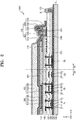
- FIG. 6 is a cross-sectional view of a display apparatus according to another embodiment.
- like reference numerals as those of FIG. 2 and FIG. 5 denote the same elements, and detailed descriptions thereof are omitted.
- the capping layer 400, the first inorganic encapsulation layer 510, and the second inorganic encapsulation layer 530 may be arranged between the barrier wall 120 and the end of the substrate 100 as described above with reference to FIG. 5 .
- the end of the capping layer 400 may be at different location from the end of the first inorganic encapsulation layer 510 (i.e., the end of the capping layer 400 may be at a location different from the location of the end of the first inorganic encapsulation layer 510).
- the end of the capping layer 400 may be extended further outward than the end of the first inorganic encapsulation layer 510 is extended in, e.g., the X-axis direction. That is, the end of the capping layer 400 may be further away from the barrier wall 120 than the end of the first inorganic encapsulation layer 510 is from the barrier wall 120 in, e.g., the X-axis direction.
- the end of the first inorganic encapsulation layer 510 may be located on an upper surface of the capping layer 400.
- the end of the capping layer 400 may be at the same location as that of the end of the second inorganic encapsulation layer 530 in, e.g., the X-axis direction.
- the end of the capping layer 400 may be further away from the barrier wall 120 than the end of the second inorganic encapsulation layer 530 is from the barrier wall 120.
- the end of the first inorganic encapsulation layer 510 and the end of the second inorganic encapsulation layer 530 may be identical in location to each other so that the end of the second inorganic encapsulation layer 530 may be closer to the barrier wall 120 than the end of the capping layer 400 is to the barrier wall 120.
- the end of the first inorganic encapsulation layer 510 and the end of the second inorganic encapsulation layer 530 are at the same location as each other will be described in more detail.
- the first inorganic encapsulation layer 510 may be firmly coupled to the capping layer 400.
- the end of the first inorganic encapsulation layer 510 is firmly coupled to the capping layer 400, and thus, infiltration of moisture and/or oxygen between the capping layer 400 and the end of the first inorganic encapsulation layer 510 may be prevented or reduced.
- FIG. 7 is a cross-sectional view of a display apparatus according to another embodiment.
- like reference numerals as those of FIG. 2 denote the same elements, and detailed descriptions thereof are omitted.
- the barrier wall 120 may at least partially cover the second line 210.
- the barrier wall 120 may cover an edge (or end) of the second line 210, which is far from (distal to) the display area DA, and may not cover an edge (or end) of the second line 210, which is close to (proximal to) the display area DA.
- the barrier wall 120 may be variously modified, e.g., the barrier wall 120 may cover the entire second line 210.
- the barrier wall 120 may prevent or reduce the organic material from flowing to the edge of the substrate 100 and prevent or block generation of an edge tail of the organic encapsulation layer 520.
- the barrier wall 120 includes a plurality of layers, in which a first layer 121 includes the same material as the planarization layer 109 and a second layer 123 on the first layer 121 may include the same material as the pixel defining layer 112.
- the planarization layer 109 and the pixel defining layer 112 may include an organic material, and the organic material has a superior (or better) adhesion to metal as compared to that of the inorganic material included in the interlayer insulating layer 107 to metal.
- the barrier wall 120 is formed to overlap the edge of the second line 210 including a metal material, the barrier wall 120 may be stably formed to have an excellent adhesion force.
- the barrier wall 120 includes the plurality of layers, but the barrier wall 120 may have a single-layered structure. In this case, the barrier wall 120 may include the same material as the planarization layer 109 or the pixel defining layer 112.
- FIG. 8 is a cross-sectional view of a display apparatus according to another embodiment.
- like reference numerals as those of FIG. 2 denote the same elements, and detailed descriptions thereof are omitted.
- the first line 116 connected to the second line 210 may extend to an upper portion of the first layer 121 in the barrier wall 120. Accordingly, a contact area between the first line 116 and the second line 210 may be increased, and a contact resistance between the second line 210 and the first line 116 may be reduced.
- the first layer 121 of the barrier wall 120 includes the same material as that of the planarization layer 109, it may be understood that the first line 116 is connected to the second line 210 via a through hole 109h penetrating through the planarization layer 109.
- the barrier wall 120 may have a structure, in which the first layer 121, the first line 116, and the second layer 123 are sequentially stacked.
- the capping layer 400 may be on the substrate 100 to shield the opposite electrode 330.
- the capping layer 400 may extend to the cutting line CL of the substrate 100 as similarly shown in FIG. 4 .
- the first inorganic encapsulation layer 510 and the second inorganic encapsulation layer 530 may be sequentially formed on the upper surface of the capping layer 400 in the same region or area (in, e.g., the X-axis direction) where the capping layer 400 is formed.
- locations of the capping layer 400, the first inorganic encapsulation layer 510, and the second inorganic encapsulation layer 530 are not limited thereto, that is, the capping layer 400, the first inorganic encapsulation layer 510, and the second inorganic encapsulation layer 530 may be arranged as in the examples shown in FIGS. 2 , 5 , and 6 .
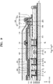
- FIG. 9 is a cross-sectional view of a display apparatus according to another embodiment.
- like reference numerals as those of FIG. 2 denote the same elements, and detailed descriptions thereof are omitted.
- the display apparatus 1000 may further include the spacer 114 on the pixel defining layer 112.
- the barrier wall 120 includes a first barrier wall 120a and a second barrier wall 120b that are spaced apart from each other.
- the spacer 114 may be further arranged on the pixel defining layer 112.
- the spacer 114 protrudes from the pixel defining layer 112 towards the thin film encapsulation layer 500, and prevents or blocks defects that are caused by mask indentations, etc., during the manufacturing processes.
- the spacer 114 may include an organic material such as polyimide, HMDSO, etc.
- the first barrier wall 120a and the second barrier wall 120b may be arranged on the second line 210 in the non-display area PA, and one of the first barrier wall 120a and the second barrier wall 120b may cover the edge of the second line 210.
- at least one of the first barrier wall 120a and the second barrier wall 120b may include a plurality of layers.
- the first barrier wall 120a includes a first layer 121a including the same material as that of the planarization layer 109 and a second layer 123a including the same material as that of the pixel defining layer 112
- the second barrier wall 120b includes a first layer 121b including the same material as that of the planarization layer 109, a second layer 123b including the same material as that of the pixel defining layer 112, and a third layer 125b including the same material as that of a spacer 114.
- the first barrier wall 120a and the second barrier wall 120b may have a single-layered structure, or both may have a dual-layered structure, a triple-layered structure, etc.
- the barrier wall may further include an additional barrier wall that is spaced apart from the first barrier wall 120a and the second barrier wall 120b.
- the barrier wall 120 includes a plurality of barrier walls, the overflow of the organic material in forming the organic encapsulation layer 520 may be effectively prevented.
- the barrier wall 120 is not limited to the above example, that is, as shown in FIGS. 7 and 8 , a single barrier wall may be formed.
- the first line 116 may be at least partially in contact with the second line 210. Here, the first line 116 may not completely shield the second line 210.
- the capping layer 400 may shield both the spacer 114 and the barrier wall 120.
- the end of the capping layer 400 may be between an outermost portion of the barrier wall 120 and the cutting line CL of the substrate 100, similarly to the example of FIG. 2 .
- the first inorganic encapsulation layer 510 and the second inorganic encapsulation layer 530 may be arranged in the same region as the capping layer 400.
- locations of the capping layer 400, the first inorganic encapsulation layer 510, and the second inorganic encapsulation layer 530 are not limited thereto, that is, the capping layer 400, the first inorganic encapsulation layer 510, and the second inorganic encapsulation layer 530 may be arranged as in the examples shown in FIGS. 4 , 5 , and 6 .
- FIG. 10 is a cross-sectional view of a display apparatus according to another embodiment.
- like reference numerals as those of FIG. 2 denote the same elements, and detailed descriptions thereof are omitted.
- the first line 116 connected to the second line 210 may extend to an upper portion of the first layer 121b in the second barrier wall 120b. Accordingly, a contact area between the first line 116 and the second line 210 may be increased, and a contact resistance between the second line 210 and the first line 116 may be reduced.
- the first layer 121b of the second barrier wall 120b includes the same material as that of the planarization layer 109, it may be understood that the first line 116 is connected to the second line 210 via the through hole 109h penetrating through the planarization layer 109.
- the second barrier wall 120b may have a structure, in which the first layer 121b, the first line 116, the second layer 123b, and a third layer 125b are sequentially stacked.
- the first barrier wall 120a may be on the first line 116 in the through hole 109h of the planarization layer 109.
- the first layer 121a of the first barrier wall 120a may include the same material as the planarization layer 109 and may be simultaneously formed with the planarization layer 109
- the second layer 123a may include the same material as the pixel defining layer 112 and may be concurrently or simultaneously formed with the pixel defining layer 112.
- a contact resistance between the first line 116 and the second line 210 may be reduced, and at the same time, a plurality of barrier walls 120 may be formed. As there are a plurality of barrier walls 120, overflow of the organic material may be effectively prevented when the organic encapsulation layer 520 is formed.
- the capping layer 400 may shield both the spacer 114 and the barrier wall 120. Here, the end of the capping layer 400 may extend to the cutting line CL of the substrate 100 similarly to the example of FIG. 4 .
- the first inorganic encapsulation layer 510 and the second inorganic encapsulation layer 530 may be arranged in the same region as the capping layer 400.
- locations of the capping layer 400, the first inorganic encapsulation layer 510, and the second inorganic encapsulation layer 530 are not limited thereto, that is, the capping layer 400, the first inorganic encapsulation layer 510, and the second inorganic encapsulation layer 530 may be arranged as in the examples shown in FIGS. 2 , 5 , and 6 .
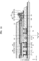
- FIG. 11 is a cross-sectional view of a display apparatus according to another embodiment.
- like reference numerals as those of FIG. 2 denote the same elements, and detailed descriptions thereof are omitted.
- the display apparatus 1000 may not include a cladding layer CCL and a slit SL.
- the capping layer 400 may be formed as shown in FIG. 2 , and the end of the capping layer 400 may be closer to the display area DA than the cutting line CL of the substrate 100.
- the first inorganic encapsulation layer 510 and the second inorganic encapsulation layer 530 may be arranged in the same region as the capping layer 400.
- locations of the capping layer 400, the first inorganic encapsulation layer 510, and the second inorganic encapsulation layer 530 are not limited thereto, that is, the capping layer 400, the first inorganic encapsulation layer 510, and the second inorganic encapsulation layer 530 may be arranged as in the examples shown in FIGS. 2 , 5 , and 6 .
- a spacer may be arranged on the pixel defining layer 112 like in the examples shown in FIGS. 9 and 10 .
- the barrier wall 120 may include a third layer 125b that is the same as the spacer, similarly to the example of FIG. 2 .
- barrier wall 120 of the embodiment is not limited to the examples shown in the drawings, but the barrier wall 120 may be identical to or similar to those of FIGS. 2 to 10 .
- FIG. 12 is a cross-sectional view of a display apparatus according to another embodiment.
- like reference numerals as those of FIG. 2 denote the same elements, and detailed descriptions thereof are omitted.
- the display apparatus 1000 may not include a cladding layer CCL and a slit SL.
- the capping layer 400 may extend to the cutting line CL of the substrate 100 as shown in FIG. 4 .
- the end of the capping layer 400 may be identical to the cutting line CL of the substrate 100.
- the first inorganic encapsulation layer 510 and the second inorganic encapsulation layer 530 may be arranged in the same region as the capping layer 400.
- locations of the capping layer 400, the first inorganic encapsulation layer 510, and the second inorganic encapsulation layer 530 are not limited thereto, that is, the capping layer 400, the first inorganic encapsulation layer 510, and the second inorganic encapsulation layer 530 may be arranged as in the examples shown in FIGS. 2 , 5 , and 6 .
- a spacer may be arranged on the pixel defining layer 112 like in the examples shown in FIGS. 9 and 10 .
- the barrier wall 120 may include a third layer 125b that is the same as the spacer, similarly to the example of FIG. 2 .
- barrier wall 120 of the embodiment is not limited to the examples shown in the drawings, but the barrier wall 120 may be identical to or similar to those of FIGS. 2 to 11 .
- the non-display area may be reduced, and infiltration of moisture and oxygen may be reduced.
- separation of the thin film encapsulation layer from the barrier wall at the portion where the barrier wall is arranged may be prevented or reduced.
- clear images displayed by the display apparatus may be realized.
Landscapes
- Chemical & Material Sciences (AREA)
- Inorganic Chemistry (AREA)
- Physics & Mathematics (AREA)
- Optics & Photonics (AREA)
- Engineering & Computer Science (AREA)
- Microelectronics & Electronic Packaging (AREA)
- Electroluminescent Light Sources (AREA)
- Devices For Indicating Variable Information By Combining Individual Elements (AREA)
Abstract
Description
- One or more embodiments relate to an apparatus, and more particularly, to a display apparatus.
- A display apparatus is an apparatus for displaying images and may include a liquid crystal display, an electrophoretic display, an organic light-emitting display, an inorganic light-emitting display, a field emission display, a surface-conduction electron-emitter display, a plasma display, a cathode ray display, etc.
- A display apparatus includes a display area and a non-display area, wherein the display area displays images and the non-display area has wires arranged therein for transferring signals to the display area. Recently, in order to realize a thin and lightweight display apparatus while maintaining high quality, research into techniques of encapsulating the display area and the non-display area by using an organic layer has been actively conducted.
- An aspect of one or more embodiments is directed toward a display apparatus having a thin film encapsulation layer that has increased adherence (e.g., may not be separated) while preventing or protecting from infiltration of external moisture and/or oxygen.
- It will be appreciated by one of ordinary skill in the art that that the objectives and effects that could be achieved with the disclosure are not limited to what has been particularly described above, and other objectives of the disclosure will be more clearly understood from the following detailed description.
- Additional aspects will be set forth in part in the description which follows and, in part, will be apparent from the description, or may be learned by practice of the presented embodiments.
- According to one or more embodiments, a display apparatus includes: a substrate including a display area for displaying images and a non-display area adjacent to (e.g., on an outer portion of) the display area; a thin film encapsulation layer including a first inorganic encapsulation layer, an organic encapsulation layer, and a second inorganic encapsulation layer stacked on the substrate; a barrier wall on the non-display area; and a capping layer between the substrate and the thin film encapsulation layer in a first direction, an end of the capping layer being located on an outer portion of the barrier wall.
- The capping layer may include an inorganic material.
- The inorganic material may include at least one selected from SiNx, TiOx, ZrOx and HfOx.
- The end of the capping layer may be closer to the barrier wall than an end of at least one of the first inorganic encapsulation layer and the second inorganic encapsulation layer is to the barrier wall in a second direction perpendicular to the first direction.
- The end of the capping layer may be farther from the barrier wall than an end of at least one of the first inorganic encapsulation layer and the second inorganic encapsulation layer is to the barrier wall in a second direction perpendicular to the first direction.
- The end of the capping layer and an end of at least one of the first inorganic encapsulation layer and the second inorganic encapsulation layer may be identical in location to each other in a second direction perpendicular to the first direction.
- At least one of the end of the capping layer, an end of the first inorganic encapsulation layer and an end of the second inorganic encapsulation layer and an end of the substrate are identical in location to each other in a second direction perpendicular to the first direction.
- The barrier wall may include: a first barrier wall on the non-display area; and a second barrier wall on the non-display area, the second barrier wall being spaced from the first barrier wall.
- The capping layer, the first inorganic encapsulation layer, and the second inorganic encapsulation layer may be sequentially stacked in the first direction on an area between the barrier wall and an end of the substrate in a second direction perpendicular to the first direction.
- The capping layer may have a refractive index of 1.8 or greater.
- According to one or more embodiments, a display apparatus includes: a substrate including a display area for displaying images and a non-display area adjuacent to (e.g., on an outer portion of) the display area; a thin film encapsulation layer including a first inorganic encapsulation layer, an organic encapsulation layer, and a second inorganic encapsulation layer stacked in a first direction on the substrate; a barrier wall on the non-display area; a cladding layer on the substrate, the cladding layer being spaced from the barrier wall towards an end of the substrate in a second direction perpendicular to the first direction; and a capping layer between the substrate and the thin film encapsulation layer in the first direction, the capping layer being at least partially located between the barrier wall and the cladding layer in the second direction.
- The capping layer may include an inorganic material.
- The inorganic material may include at least one selected from SiNx, TiOx, ZrOx, and HfOx.
- An end of the capping layer may be between the barrier wall and the cladding layer in the second direction.
- An end of the capping layer and an end of the substrate are identical in location to each other in the second direction.
- An end of the capping layer may be at a location different from an end of at least one of the first inorganic encapsulation layer and the second inorganic encapsulation layer in the second direction, or the end of the capping layer may be at a same location as the end of at least one of the first inorganic encapsulation layer and the second inorganic encapsulation layer in the second direction.
- The capping layer, the first inorganic encapsulation layer, and the second inorganic encapsulation layer may be sequentially stacked in the first direction on an area between the barrier wall and an end of the substrate in the second direction.
- According to one or more embodiments, a display apparatus includes: a substrate including a display area for displaying images and a non-display area adjacent to (e.g., on an outer portion of) the display area; a thin film encapsulation layer including a first inorganic encapsulation layer, an organic encapsulation layer, and a second inorganic encapsulation layer stacked on the substrate; a barrier wall on the non-display area; and a capping layer between the substrate and the thin film encapsulation layer, the capping layer covering a front surface of the barrier wall, and the capping layer including an inorganic material.
- A density of the capping layer may be greater than a density of at least one of the first inorganic encapsulation layer and the second inorganic encapsulation layer.
- The capping layer may have a thickness of 1000 Å or less.
- At least some of the above and other features of the invention are set out in the claims.
- Other aspects, features, and advantages of the disclosure will become better understood through the accompanying drawings, the claims, and the detailed description.
- Such general and specific aspects of the disclosure may be performed using systems, methods, computer-readable storage mediums, and/or combinations thereof.
- These and/or other aspects will become apparent and more readily appreciated from the following description of the embodiments, taken in conjunction with the accompanying drawings in which:
-
FIG. 1 is a plan view of a display apparatus according to an embodiment; -
FIG. 2 is a cross-sectional view taken along a line II-II' ofFIG. 1 ; -
FIG. 3 is a cross-sectional view showing a relationship between the display apparatus ofFIG. 2 and a mask used in manufacturing the display apparatus; -
FIG. 4 is a cross-sectional view of a display apparatus according to another embodiment; -
FIG. 5 is a cross-sectional view of a display apparatus according to another embodiment; -
FIG. 6 is a cross-sectional view of a display apparatus according to another embodiment; -
FIG. 7 is a cross-sectional view of a display apparatus according to another embodiment; -
FIG. 8 is a cross-sectional view of a display apparatus according to another embodiment; -
FIG. 9 is a cross-sectional view of a display apparatus according to another embodiment; -
FIG. 10 is a cross-sectional view of a display apparatus according to another embodiment; -
FIG. 11 is a cross-sectional view of a display apparatus according to another embodiment; and -
FIG. 12 is a cross-sectional view of a display apparatus according to another embodiment. - Reference will now be made in more detail to embodiments, examples of which are illustrated in the accompanying drawings, wherein like reference numerals refer to like elements throughout. In this regard, the present embodiments may have different forms and should not be construed as being limited to the descriptions set forth herein. Accordingly, the embodiments are merely described below, by referring to the figures, to explain aspects of the present description. As used herein, the term "and/or" includes any and all combinations of one or more of the associated listed items. Expressions such as "at least one of," "one of," "selected from," "at least one selected from," and "one selected from," when preceding a list of elements, modify the entire list of elements and do not modify the individual elements of the list. Further, the use of "may" when describing embodiments of the present disclosure refers to "one or more embodiments of the present disclosure."
- The example embodiments will be described below in more detail with reference to the accompanying drawings. Those components that are the same or are in correspondence are rendered with like reference numerals regardless of the figure number, and redundant explanations are not provided again.
- While such terms as "first," "second," etc., may be used to describe various components, such components are not to be limited to the above terms. The above terms are used only to distinguish one component from another.
- An expression used in the singular encompasses the expression of the plural, unless it has a clearly different meaning in the context.
- In the present specification, it is to be understood that the terms "including," "having," and "comprising" are intended to indicate the existence of the features, numbers, steps, actions, components, parts, or combinations thereof disclosed in the specification, and are not intended to preclude the possibility that one or more other features, numbers, steps, actions, components, parts, or combinations thereof may exist or may be added.
- It should be understood that when an element such as a layer, film, region, or substrate is referred to as being "on" another element, it can be directly on the other element or intervening element(s) may also be present. In contrast, when an element is referred to as being "directly on" another element, no intervening elements are present.
- Sizes of components in the drawings may be exaggerated for convenience of explanation. In other words, since sizes and thicknesses of components in the drawings are arbitrarily illustrated for convenience of explanation, the following embodiments are not limited thereto.
- The X-axis, the Y-axis, and the Z-axis are not limited to three axes of the rectangular coordinate system, and may be interpreted in a broader sense. For example, the X-axis, the Y-axis, and the Z-axis may be perpendicular to one another, or may represent different directions that are not perpendicular to one another.
- When a certain embodiment may be implemented differently, a specific process order may be performed differently from the described order. For example, two consecutively described processes may be performed substantially at the same time or performed in an order opposite to the described order.
-
FIG. 1 is a plan view of a display apparatus according to an embodiment.FIG. 2 is a cross-sectional view taken along a line II-II' ofFIG. 1 .FIG. 3 is a cross-sectional view showing a relationship between the display apparatus ofFIG. 2 and a mask used in manufacturing the display apparatus. - Referring to
FIGS. 1 to 3 , thedisplay apparatus 1000 includes asubstrate 100. Thesubstrate 100 includes a display area DA and a non-display area PA adjacent to the display area DA. - A plurality of pixels are arranged in the display area DA of the
substrate 100 to display images. Various display devices (such as an organic light-emitting device (OLED), a thin film transistor, a capacitor, etc.) may be arranged in the display area DA, and pixels (formed by electrical combination of the display devices, the thin film transistor, the capacitor, etc.) display images. A driving current flowing through the display devices is generated according to a gate signal, a data signal, a driving voltage (ELVDD), a common voltage (ELVSS), etc., supplied to the pixel, and the display device may emit light having a luminance corresponding to the driving current. - The non-display area PA is adjacent to the display area DA. A
wiring portion 600 for supplying various signals and/or power source applied to the display area DA may be arranged in the non-display area PA. Thewiring portion 600 may include a drive circuit. For example, the drive circuit may include at least one selected from a scan driving circuit, a terminal portion, a driving power supply line, and asecond line 210, and may further include a thin film transistor T3 for controlling electrical signals applied to the display area DA. Also, a barrier wall or a trench may be arranged in the non-display area PA, and the barrier wall or the trench may block a flow of an organic layer that is used to manufacture thedisplay apparatus 1000. In this case, at least one selected from the scan driving circuit, the terminal portion, the driving power supply line, thesecond line 210, and the thin film transistor T3 may be arranged in the non-display area PA at a longer side of the display apparatus 1000 (e.g., the longer side being parallel to the Y-axis) or the non-display area PA at a shorter side of the display apparatus 1000 (e.g., the shorter side being parallel to the X-axis). - The
display apparatus 1000 includes thesubstrate 100 including the display area DA and the non-display area PA, and a thinfilm encapsulation layer 500 for encapsulating the display area DA and the non-display area PA. - The
substrate 100 may include various materials. For example, thesubstrate 100 may include a transparent glass material containing SiO2 as a main component. However, thesubstrate 100 is not limited thereto, that is, it may include a transparent plastic material. The plastic material may include an insulating organic material, that is, an organic material selected from the group consisting of a polyether sulfone, polyacrylate, polyetherimide, polyethylene naphthalate, polyethylene terephthalate, polyphenylene sulfide, polyarylate, polyimide, polycarbonate, cellulose triacetate, cellulose acetate propionate, etc. Also, thesubstrate 100 may have a multi-layered structure including a layer including the plastic material and an inorganic layer. - A
buffer layer 101 is located on thesubstrate 100 to reduce or block infiltration of impurities, moisture, or external air from a lower portion of thesubstrate 100, and to provide a flat surface on thesubstrate 100. Thebuffer layer 101 may include an inorganic material (such as an oxide material and/or a nitride material), an organic material, or an inorganic-organic composite material, and may have a single-layered or multi-layered structure including the inorganic material and/or the organic material. - A first thin film transistor T1 includes a semiconductor layer A1, a first gate electrode G1, a source electrode S1, and a drain electrode D1, and a second thin film transistor T2 includes a semiconductor layer A2, a second gate electrode G2, a source electrode S2, and a drain electrode D2.
- Hereinafter, the thin film transistors T1 and T2 are top gate type. However, the embodiment is not limited thereto, and thin film transistors of various types such as a bottom gate type may be adopted.
- Also, hereinafter, a case in which two thin film transistors T1 and T2 is described, but one or more embodiments are not limited thereto. In one or more embodiments, the
display apparatus 1000 may include two or more thin film transistors T1 and T2 in one pixel. In some embodiments, six or seven thin film transistors may be adopted in one pixel. - The semiconductor layers A1 and A2 may each include amorphous silicon or polycrystalline silicon. In another embodiment, the semiconductor layers A1 and A2 may each include an oxide of at least one selected from the group consisting of indium (In), gallium (Ga), tin (Sn), zirconium (Zr), vanadium (V), hafnium (Hf), cadmium (Cd), germanium (Ge), chromium (Cr), titanium (Ti), and zinc (Zn). The semiconductor layers A1 and A2 may include a channel region and a source region and a drain region having higher carrier concentrations than the channel region.
- The first gate electrode G1 is arranged on the semiconductor layer A1 with a first
gate insulating layer 103 therebetween. The first gate electrode G1 may include molybdenum (Mo), aluminium (Al), copper (Cu), titanium (Ti), etc., and may have a single-layered or multi-layered structure. As an example, the first gate electrode G1 may have a single layer including Mo. - The first
gate insulating layer 103 is provided to insulate the semiconductor layer A1 from the first gate electrode G1, and may include silicon oxide (SiO2), silicon nitride (SiNx), silicon oxynitride (SiON), aluminium oxide (Al2O3), titanium oxide (TiO2), tantalum oxide (Ta2O5), hafnium oxide (HfO2), zinc oxide (ZnO2), etc. - The second gate electrode G2 is on the semiconductor layer A2 with the first
gate insulating layer 103 and a secondgate insulating layer 105 therebetween. The second gate electrode G2 may include a conductive material including molybdenum (Mo), aluminium (Al), copper (Cu), titanium (Ti), etc., and may have a single-layered or multi-layered structure. As an example, the second gate electrode G2 may have a single layer including Mo or a multi-layered structure including Mo/AI/Mo. - The second
gate insulating layer 105 may include an inorganic material including an oxide and/or a nitride. For example, the secondgate insulating layer 105 may include silicon oxide (SiO2), silicon nitride (SiNx), silicon oxynitride (SiON), aluminium oxide (Al2O3), titanium oxide (TiO2), tantalum oxide (Ta2O5), hafnium oxide (HfO2), and/or zinc oxide (ZnO2). - The source electrodes S1 and S2 and the drain electrodes D1 and D2 are arranged on an
interlayer insulating layer 107. The source electrodes S1 and S2 and the drain electrodes D1 and D2 may each include a conductive material including Mo, Al, Cu, Ti, etc., and may have a single-layered or multi-layered structure including the above material(s). For example, the source electrodes S1 and S2 and the drain electrodes D1 and D2 may each have a multi-layered structure including Ti/AI/Ti. - The interlayer insulating
layer 107 may include silicon oxide (SiO2), silicon nitride (SiNx), silicon oxynitride (SiON), aluminium oxide (Al2O3), titanium oxide (TiO2), tantalum oxide (Ta2O5), hafnium oxide (HfO2), zinc oxide (ZnO2), etc. - As described above, the first gate electrode G1 of the first thin film transistor T1 and the second gate electrode G2 of the second thin film transistor T2 may be at different layers. Accordingly, the first thin film transistor T1 and the second thin film transistor T2 may have different operating ranges.
- A first electrode CE1 of a storage capacitor Cst may include the same material at the same layer as the first gate electrode G1. A second electrode CE2 of the storage capacitor Cst overlaps the first electrode CE1 with the second
gate insulating layer 105 therebetween. The second electrode CE2 may include the same material at the same layer as the second gate electrode G2. - In
FIG. 2 , the storage capacitor Cst does not overlap the first thin film transistor T1 and the second thin film transistor T2. However, one or more embodiments are not limited thereto. For example, the storage capacitor Cst may overlap the first thin film transistor T1. In some embodiments, the first electrode CE1 of the storage capacitor Cst may be integrally formed with the first gate electrode G1. That is, the first gate electrode G1 of the first thin film transistor T1 may also function (e.g., be configured) as the first electrode CE1 of the storage capacitor Cst. - A
planarization layer 109 is on the source electrodes S1 and S2 and the drain electrodes D1 and D2, and an organic light-emitting diode OLED may be on theplanarization layer 109. Theplanarization layer 109 may include a single-layered or multi-layered structure including an organic material. The organic material may include or be at least one selected from general-purpose polymers (e.g., polymethylmethacrylate (PMMA) and/or polystyrene (PS)), polymer derivatives having phenol groups, acryl-based polymers, imide-based polymers, aryl ether-based polymers, amide-based polymers, fluoride-based polymers, p-xylene-based polymers, vinyl alcohol-based polymers, and blends thereof. Also, theplanarization layer 109 may have a composite stack structure including an inorganic insulating layer and an organic insulating layer. - An organic light-emitting diode (OLED) 300 may be on the
planarization layer 109 in the display area DA of thesubstrate 100. The organic light-emittingdiode 300 may include apixel electrode 310, anopposite electrode 330, and anintermediate layer 320 between thepixel electrode 310 and theopposite electrode 330. - The
pixel electrode 310 is in contact with one of the source electrode S1 and the drain electrode D1 of the first thin film transistor T1 via an opening formed in theplanarization layer 109 to be electrically connected to the first thin film transistor T1. Thepixel electrode 310 may be a reflective electrode. For example, thepixel electrode 310 may include a reflective layer including Ag, Mg, Al, Pt, Pd, Au, Ni, Nd, Ir, Cr, and/or a compound thereof, and a transparent or semi-transparent electrode layer on the reflective layer. The transparent or semi-transparent electrode layer may include at least one selected from the group consisting of indium tin oxide (ITO), indium zinc oxide (IZO), zinc oxide (ZnO), indium oxide (In2O3), indium gallium oxide, and aluminium zinc oxide (AZO). - A
pixel defining layer 112 may be on theplanarization layer 109. Thepixel defining layer 112 includes an opening corresponding to each sub-pixel, that is, an opening that exposes at least a center of thepixel electrode 310, to define pixels. Also, thepixel defining layer 112 increases a distance between an edge of thepixel electrode 310 and theopposite electrode 330 on thepixel electrode 310 to prevent (or protect from) generation of arc at the edge of thepixel electrode 310. Thepixel defining layer 112 may include an organic material, for example, polyimide, hexamethyl disiloxane (HMDSO), etc. - The
intermediate layer 320 of the organic light-emitting diode may include a low-molecular weight organic material or a polymer material. When theintermediate layer 320 includes a low-molecular weight material, theintermediate layer 320 may include a hole injection layer (HIL), a hole transport layer (HTL), an emission layer (EML), an electron transport layer (ETL), and/or an electron injection layer (EIL) in a single-layered or multi-layered structure, and examples of the low-molecular weight material may include copper phthalocyanine (CuPc), N,N'-di(naphthalene-1-yl)-N,N'-diphenyl-benzidine (NPB), and tris-8-hydroxyquinoline aluminium (Alq3). The above layers may be manufactured by a vacuum deposition method. - When the
intermediate layer 320 includes a polymer material, theintermediate layer 320 may include an HTL and/or an EML. Here, the HTL may include poly(3,4-ethylenedioxythiophene) PEDOT, and the EML may include a poly-phenylenevinylene (PPV)-based or polyfluorene-based polymer material. Theintermediate layer 320 may be obtained by a screen printing method, an inkjet printing method, a laser induced thermal imaging (LITI) method, a vacuum deposition method using a mask, etc. - However, the
intermediate layer 320 is not limited thereto, but may have various structures. In addition, theintermediate layer 320 may be formed integrally throughout the plurality ofpixel electrodes 310 or may be patterned to correspond to each of the plurality ofpixel electrodes 310. - The
opposite electrode 330 is arranged above the display area DA and may cover the display area DA as shown inFIG. 2 . That is, theopposite electrode 330 may be integrally provided throughout the plurality of organic light-emittingdiodes 300 to correspond to a plurality ofpixel electrodes 310. In another embodiment, theopposite electrode 330 may cover the display area DA and partially cover the non-display area PA. Hereinafter, for convenience of description, a case in which theopposite electrode 330 covers the display area DA and partially covers the non-display area PA will be described in more detail. - The
opposite electrode 330 may be a transmissive electrode. For example, theopposite electrode 330 may be a transparent or a semi-transparent electrode, and may be provided as a metal thin film including Li, Ca, LiF/Ca, LiF/Al, Al, Ag, Mg, and a compound thereof having a small work function. Also, a transparent conductive oxide (TCO) (such as ITO, IZO, ZnO, and/or In2O3) may be further provided over the metal thin film. - As the
pixel electrode 310 is a reflective electrode and theopposite electrode 330 is a transmissive electrode, light emitted from theintermediate layer 320 is emitted towards theopposite electrode 330, that is, a top emission type. However, one or more embodiments are not limited thereto, and the light emitted from theintermediate layer 320 may be emitted towards thesubstrate 100, that is, a bottom emission type. In this case, thepixel electrode 310 may be a transparent or semi-transparent electrode, and theopposite electrode 330 may be a reflective electrode. Alternatively, the display apparatus according to the embodiment may be a dual-emission type in which light is emitted to the top and bottom surfaces of thedisplay apparatus 1000. - A
capping layer 400 may be on theopposite electrode 330. Here, thecapping layer 400 may be in direct contact with theopposite electrode 330. Thecapping layer 400 may have a refractive index that is lower than that of the opposite electrode and higher than that of the firstinorganic encapsulation layer 510. Thecapping layer 400 may improve an optical efficiency by reducing a ratio of the light that may not be emitted to outside due to total reflection, when the light is emitted from theintermediate layer 320 including the organic emission layer. - The
capping layer 400 may include or be composed of an inorganic material. For example, the inorganic material may include or be zinc oxide, titanium oxide, zirconium oxide, silicon nitride, niobium oxide, tantalum oxide, tin oxide, nickel oxide, indium nitride, and/or gallium nitride. For example, the inorganic material may include at least one selected from SiNx, TiOx, ZrOx and HfOx. - The
capping layer 400 may have a refractive index greater than that of the firstinorganic encapsulation layer 510. For example, the refractive index of thecapping layer 400 may be greater than that of the firstinorganic encapsulation layer 510 by 0.24 or greater. Here, when a difference between the refractive index of thecapping layer 400 and the refractive index of the firstinorganic encapsulation layer 510 is less than 0.24, a lot of total reflection occurs on a boundary between thecapping layer 400 and the firstinorganic encapsulation layer 510 or light corresponding to a resonant frequency of the emission layer may not be transmitted, and thereby luminance degrades. In this case, thecapping layer 400 may have a refractive index of 1.8 or greater. When the refractive index of thecapping layer 400 is less than 1.8, as described above, the light is reflected between the firstinorganic encapsulation layer 510 and thecapping layer 400 and the luminance of the emission layer is reduced. - Also, in the above case, the
capping layer 400 may have a thickness of 1000 Å or less. In more detail, a thickness of thecapping layer 400 may be measured based on a Z-axis direction inFIG. 2 . Here, when the thickness of thecapping layer 400 is greater than 1000 Å, it may take a lot of time and energy to form thecapping layer 400. Moreover, when the thickness of thecapping layer 400 is greater than 1000 Å, the light emitted from the emission layer may not transmit through thecapping layer 400 or a wavelength of the light is variable, and thus, it may be difficult to obtain clear images. - The
capping layer 400 may be deposited on thesubstrate 100 by an atomic layer deposition (ALD) method. In this case, a mask may be used to form thecapping layer 400. Such a mask may have an opening to expose the non-display area PA partially and the display area DA. - A density of the
capping layer 400 may be greater than that of the firstinorganic encapsulation layer 510. In this case, when thecapping layer 400 is at the surface of thebarrier wall 120, a coupling force between thecapping layer 400 and thebarrier wall 120 may be greater than that between the firstinorganic encapsulation layer 510 and thebarrier wall 120. In this case, thecapping layer 400 and the firstinorganic encapsulation layer 510 may not be lifted from thebarrier wall 120 at a bent portion of thebarrier wall 120. Therefore, thecapping layer 400 is densely formed or arranged in material on the surface of the barrier wall 120 (formed of or including the organic material) to be coupled to the surface of thebarrier wall 120, and thus, thecapping layer 400 may not be separated from thebarrier wall 120 and the firstinorganic encapsulation layer 510 may not be separated from thecapping layer 400, due to external shock and/or external force applied thereto. - The
capping layer 400 may also shield thebarrier wall 120. For example, an end of thecapping layer 400 may be closer to an edge (or end) of the substrate 100 (or cutting line CL) than an outermost portion of thebarrier wall 120 is to the edge (or end) of thesubstrate 100. In this case, the end of thecapping layer 400 may be between thebarrier wall 120 and the edge of thesubstrate 100. In another embodiment, the end of thecapping layer 400 may be identical in location to the edge of the substrate 100 (or the cutting line CL or an end of the substrate 100) in, e.g., the X-axis direction. Hereinafter, for convenience of description, a case in which the end of thecapping layer 400 is between thebarrier wall 120 and the edge of thesubstrate 100 will be described below. - As described above, when the end of the
capping layer 400 is arranged beyond the outer portion of thebarrier wall 120 in, e.g., the X-axis direction, a passage (through which external moisture and/or oxygen is introduced into the display area DA between thecapping layer 400 and thesubstrate 100 or between thecapping layer 400 and another insulating layer) may increase and it may protect from or make it more difficult for the moisture and/or oxygen to infiltrate into the display area DA. Moreover, because thecapping layer 400 has a high density, thecapping layer 400 may be firmly coupled to thesubstrate 100 or another layer, and thus thecapping layer 400 may not be separated from thesubstrate 100 or another layer. The thickness of thecapping layer 400 may be less than that of the firstinorganic encapsulation layer 510. For example, the thickness of thecapping layer 400 may be 1000 Å or less, and the firstinorganic encapsulation layer 510 may have a thickness of 1 µm to 1.5 µm. In particular, because luminance and wavelength of the light emitted from the emission layer are dependent upon the thickness of thecapping layer 400, the luminance of the light may degrade or the wavelength of the light emitted from the emission layer may vary depending on the difference between the refractive index of thecapping layer 400 and the refractive index of the firstinorganic encapsulation layer 510 when the thickness of thecapping layer 400 is greater than that of the firstinorganic encapsulation layer 510. Therefore, thecapping layer 400 may have a thickness less than that of the firstinorganic encapsulation layer 510. - The thin
film encapsulation layer 500 covers the display area DA and the non-display area PA to prevent (or protect from) infiltration of the external moisture and/or oxygen. The thinfilm encapsulation layer 500 may include at least one organic encapsulation layer and at least one inorganic encapsulation layer. InFIG. 2 , the thinfilm encapsulation layer 500 includes first and second inorganic encapsulation layers 510 and 530 and oneorganic encapsulation layer 520, but stacking order and the number of stacking layers may not be limited to the example ofFIG. 2 . - The first
inorganic encapsulation layer 510 covers theopposite electrode 330, and may include silicon oxide, silicon nitride, and/or silicon oxynitride. If necessary, other layers such as thecapping layer 400 may be provided between the firstinorganic encapsulation layer 510 and theopposite electrode 330. Because the firstinorganic encapsulation layer 510 is arranged along a lower structure thereof, as shown inFIG. 2 , the firstinorganic encapsulation layer 510 may have an upper surface that is not flat. Theorganic encapsulation layer 520 covers the firstinorganic encapsulation layer 510, and unlike the firstinorganic encapsulation layer 510, theorganic encapsulation layer 520 may have a flat upper surface. In more detail, theorganic encapsulation layer 520 may planarize the upper surface of a portion corresponding to the display area DA. Theorganic encapsulation layer 520 may include one or more materials selected from the group consisting of polyethylene terephthalate, polyethylene naphthalate, polycarbonate, polyimide, polyethylene sulfonate, polyoxymethylene, polyarylate, and hexamethyl disiloxane. The secondinorganic encapsulation layer 530 covers theorganic encapsulation layer 520, and may include silicon oxide, silicon nitride, and/or silicon oxynitride. - As described above, because the thin
film encapsulation layer 500 includes the firstinorganic encapsulation layer 510, theorganic encapsulation layer 520, and the secondinorganic encapsulation layer 530, even when cracks occur in the thinfilm encapsulation layer 500, the cracks may be disconnected between the firstinorganic encapsulation layer 510 and theorganic encapsulation layer 520 or between theorganic encapsulation layer 520 and the secondinorganic encapsulation layer 530 through the multi-layered structure. As such, generation of an infiltration path through which the external moisture or oxygen passes to the display area DA and the non-display area PA may be prevented or reduced. The secondinorganic encapsulation layer 530 contacts the firstinorganic encapsulation layer 510 at an edge thereof on an outer portion of the display area DA (e.g., at where theorganic encapsulation layer 520 ends), and theorganic encapsulation layer 520 may not be exposed to outside. - At least one of the first
inorganic encapsulation layer 510 and the secondinorganic encapsulation layer 530 may be formed by a chemical vapor deposition method. Here, an end of at least one of the firstinorganic encapsulation layer 510 and the secondinorganic encapsulation layer 530 may be or may not be identical to the end of thecapping layer 400. For example, in an embodiment, the end of at least one of the firstinorganic encapsulation layer 510 and the secondinorganic encapsulation layer 530 may coincide with the end of the capping layer 400 (e.g., coincide or be identical in location along the X-axis). In another embodiment, the end of at least one of the firstinorganic encapsulation layer 510 and the secondinorganic encapsulation layer 530 may be closer to or further from the edge of thesubstrate 100 than the end of thecapping layer 400 is to the edge of thesubstrate 100. - In particular, the end of the first
inorganic encapsulation layer 510 and the end of the secondinorganic encapsulation layer 530 may be identical to or different from each other (e.g., identical to or different in location along the X-direction). In an embodiment, the end of the firstinorganic encapsulation layer 510 may be closer to the edge of thesubstrate 100 than the end of the secondinorganic encapsulation layer 530. In another embodiment, the end of the firstinorganic encapsulation layer 510 may be identical to the end of the secondinorganic encapsulation layer 530. Hereinafter, for the convenience of description, a case in which the end of the firstinorganic encapsulation layer 510 is identical to the end of the secondinorganic encapsulation layer 530 will be described in more detail. - In the above case, the first
inorganic encapsulation layer 510 may be in direct contact with thecapping layer 400 on thebarrier wall 120. In more detail, thecapping layer 400, the firstinorganic encapsulation layer 510, and the secondinorganic encapsulation layer 530 may be sequentially stacked on thebarrier wall 120. In particular, because thebarrier wall 120 has a protrusion, an inclination may occur, and a hole (or recess) may be generated between theplanarization layer 109 and thebarrier wall 120 or between the plurality ofbarrier walls 120. When the firstinorganic encapsulation layer 510 is formed in a state where thecapping layer 400 does not exist in the hole, the firstinorganic encapsulation layer 510 and theopposite electrode 330 may be separated from each other, thebarrier wall 120 and the firstinorganic encapsulation layer 510 may be separated from each other, or thebarrier wall 120 and theplanarization layer 109 may be separated from each other, when external power is applied to thebarrier wall 120 or to a region of thesubstrate 100 that is located inside (or defined by) thebarrier wall 120. However, as described above, because thecapping layer 400 is arranged over the display area DA and the partial region of the non-display area PA, inside thebarrier wall 120, the firstinorganic encapsulation layer 510 may not directly contact thebarrier wall 120, theplanarization layer 109, and theopposite electrode 330. In this case, due to the high density of thecapping layer 400, thecapping layer 400 may be firmly coupled to thebarrier wall 120, theplanarization layer 109, and theopposite electrode 330, and thus thecapping layer 400 may not be separated from thebarrier wall 120, theplanarization layer 109, and theopposite electrode 330. Moreover, because the firstinorganic encapsulation layer 510 and thecapping layer 400 both include the inorganic material, a coupling force between thecapping layer 400 and the firstinorganic encapsulation layer 510 may increase and the firstinorganic encapsulation layer 510 may not be separated from thecapping layer 400. Therefore, when thecapping layer 400 is on (or under) a lower surface of the firstinorganic encapsulation layer 510 as described above, lifting-off of the firstinorganic encapsulation layer 510 may be reduced as compared with a case where thecapping layer 400 does not exist on the non-display area PA that is located at the inner portion of (or defined by) thebarrier wall 120. - Also, as described above, because the ends of the
capping layer 400, the firstinorganic encapsulation layer 510, and the secondinorganic encapsulation layer 530 are identical to one another in location, the moisture and/or oxygen introduced into the display area DA may be effectively blocked. - A
first line 116 is at the same layer as thepixel electrode 310, and, as shown inFIG. 2 , may be arranged on a flat surface of theplanarization layer 109 and thebarrier wall 120. Here, thefirst line 116 may be formed concurrently or simultaneously with thepixel electrode 310 by using the same material as that included in thepixel electrode 310. In this case, thefirst line 116 may be connected to theopposite electrode 330, and by increasing a contact area with respect to theopposite electrode 330, the common voltage ELVSS may be stably supplied to theopposite electrode 330 with asecond line 210. Then, at least a part of thefirst line 116 may partially or totally shield thesecond line 210. In particular, thefirst line 116 may cover a front surface of thesecond line 210 and may extend to an upper portion of some layers in thebarrier wall 120. - In addition to the above case, the
second line 210, thebarrier wall 120, and a cladding layer CCL are arranged in the non-display area PA of thesubstrate 100. Thesecond line 210 may be a wiring for supplying electric power to the display area DA, and may be at the same layer as the source electrodes S1 and S2 and the drain electrodes D1 and D2 and may include the same material as that of the source electrodes S1 and S2 and the drain electrodes D1 and D2. In some embodiments, thesecond line 210 may be connected to theopposite electrode 330 of the organic light-emitting diode (OLED) 300 to transmit the common voltage ELVSS. In an embodiment, thesecond line 210 may be directly connected to theopposite electrode 330 that is extended. In another embodiment, as shown inFIG. 2 , thesecond line 210 may be connected to theopposite electrode 330 via thefirst line 116. In this case, thefirst line 116 may be formed concurrently or simultaneously with thepixel electrode 310 by using the same material as that included in thepixel electrode 310. However, one or more embodiments are not limited thereto, that is, thesecond line 210 may be connected to theopposite electrode 330 in various manners. Hereinafter, for convenience of description, a case in which thesecond line 210 is connected to theopposite electrode 330 via thefirst line 116 will be described in more detail. - The
barrier wall 120 may at least partially cover thesecond line 210. In some embodiments, thebarrier wall 120 may cover an edge (or end) of thesecond line 210, which is far from (or distal to) the display area DA, and may not cover an edge (or end) of thesecond line 210, which is close to (or proximal to) the display area DA. However, one or more embodiments are not limited thereto. That is, thebarrier wall 120 may be variously modified, e.g., thebarrier wall 120 may cover the entiresecond line 210. - When the
organic encapsulation layer 520 of the thinfilm encapsulation layer 500 for encapsulating the display area DA and the non-display area PA is being formed, thebarrier wall 120 may prevent (or protect from) the organic material from flowing to the edge of thesubstrate 100 and prevent (or reduce) generation of an edge tail of theorganic encapsulation layer 520. - The
barrier wall 120 includes afirst barrier wall 120a and asecond barrier wall 120b that are spaced apart from each other. - The
first barrier wall 120a and thesecond barrier wall 120b may be arranged on thesecond line 210 in the non-display area PA, and one of thefirst barrier wall 120a and thesecond barrier wall 120b may cover the edge of thesecond line 210. In addition, at least one of thefirst barrier wall 120a and thesecond barrier wall 120b may include a plurality of layers. InFIG. 2 , thefirst barrier wall 120a includes afirst layer 121a including the same material as that of theplanarization layer 109 and asecond layer 123a including the same material as that of thepixel defining layer 112, and thesecond barrier wall 120b includes afirst layer 121b including the same material as that of theplanarization layer 109, asecond layer 123b including the same material as that of thepixel defining layer 112, and athird layer 125b including the same material as that of a spacer. The spacer may include an organic material such as polyimide, HMDSO, etc. However, one or more embodiments are not limited thereto. That is, one of thefirst barrier wall 120a and thesecond barrier wall 120b may have a single-layered structure, or both may have a dual-layered structure, a triple-layered structure, etc. Also, the barrier wall may further include an additional barrier wall that is spaced apart from thefirst barrier wall 120a and thesecond barrier wall 120b. - Because the
barrier wall 120 includes a plurality of barrier walls, the overflow of the organic material in forming theorganic encapsulation layer 520 may be effectively prevented. - The
first line 116 connected to thesecond line 210 may extend to an upper portion of thefirst layer 121b in thesecond barrier wall 120b. Accordingly, a contact area between thefirst line 116 and thesecond line 210 may be increased, and a contact resistance between thesecond line 210 and thefirst line 116 may be reduced. When thefirst layer 121b of thesecond barrier wall 120b includes the same material as that of theplanarization layer 109, it may be understood that thefirst line 116 is connected to thesecond line 210 via a throughhole 109h penetrating through theplanarization layer 109. - The cladding layer CCL is on the
substrate 100 to cover a slit SL. In another embodiment, the cladding layer CCL may be formed on thebuffer layer 101 on thesubstrate 100. Hereinafter, for convenience of description, a case in which the cladding layer CCL is formed on thesubstrate 100 will be described in more detail. - In an alternative embodiment, a width of the cladding layer CCL may be greater than that of the slit SL, and a length of the cladding layer CCL may be greater than that of the slit SL. As such, the cladding layer CCL may completely embed the slit SL, so as not to expose the slit SL.
- The cladding layer CCL may include various materials. That is, the cladding layer CCL may include an inorganic material and/or an organic material.
- In an alternative embodiment, the cladding layer CCL may include an organic material. As such, appropriate width and thickness of the cladding layer CCL may be obtained easily, and the slit SL may be easily covered.
- In an alternative embodiment, the cladding layer CCL may include a material that is the same as that of an insulating layer (not shown) that may be formed in the non-display area PA of the
substrate 100. Also, the cladding layer CCL may be formed concurrently or simultaneously with an insulating layer (not shown) that may be formed in the display area DA of thesubstrate 100. For example, the cladding layer CCL may include the same material as that of theplanarization layer 109 and/or thepixel defining layer 112. - The cladding layer CCL may be formed in the non-display area PA.
- In an alternative embodiment, the cladding layer CCL may be arranged at the edge (or end) of the
substrate 100 or on a boundary (or area) between the cutting line CL and the display area DA in, e.g., the X-axis direction. - The cladding layer CCL may be elongated. That is, the cladding layer CCL may extend or be elongated in a direction parallel with the cutting line CL of the substrate 100 (or longer side or shorter side of the substrate 100) shown in
FIG. 1 . Here, the cladding layer CCL may have a variable length, and the length of the cladding layer CCL may be greater or less than the length of the display area DA. - The non-display area PA of the
display apparatus 1000 may include the slit SL. Here, the slit SL may be obtained by partially removing at least one of the inorganic layer and the organic layer on thesubstrate 100. The slit SL blocks the cracks propagated from the edge of thesubstrate 100. For example, the slit SL adjacent to the cutting line CL of thesubstrate 100 may primarily prevent or block propagation of cracks that may occur in thesubstrate 100 when a mother substrate is cut and divided intoindividual display apparatuses 1000. - In particular, according to some embodiments, the slit SL may be formed on the
buffer layer 101. In this case, thebuffer layer 101 on thesubstrate 100 is arranged in the non-display area PA, and/or may extend to the cutting line CL so as to protect the upper surface of thesubstrate 100. Also, the slit SL may block or reduce occurrence or propagation of cracks that may occur in thebuffer layer 101 due to a pressure applied to thebuffer layer 101. - The cladding layer CCL is formed on the slit SL. The cladding layer CCL may prevent or reduce movement of impurities and/or particles that may be generated on the slit SL. In one embodiment, the cladding layer CCL may cover the slit SL to block or not expose impurities and/or particles remaining in the slit SL.
- Impurities and/or particles may be generated in the slit SL when the
display apparatus 1000 is manufactured. For example, during manufacturing of thedisplay apparatus 1000, a conductive material used to form an electrode may remain in the slit SL. The conductive material remaining in the slit SL may cause defects in thedisplay apparatus 1000 in post-processes, for example, the conductive material may move to the display area DA and cause electrical defects in the display area DA, which may degrade electrical characteristics and image quality of thedisplay apparatus 1000. - The cladding layer CCL is formed on the slit SL to prevent or reduce movement of the remaining impurities and particles, and thus may prevent or reduce defects that may occur in the display area DA.
- Also, separation of the cladding layer CCL from the
substrate 100 may be prevented or reduced by the slit SL. - In addition, in a method of manufacturing the
display apparatus 1000 as described above, each layer is formed on thesubstrate 100, and then theopposite electrode 330 may be arranged on the display area DA and partially on the non-display area PA. - After forming the
opposite electrode 330, thecapping layer 400 may be formed. Here, thecapping layer 400 may be formed by using an ALD apparatus, as described above. In particular, thecapping layer 400 may be formed by using a first mask M1 having a first opening OP1. The first opening OP1 may have an area that is greater than that of the display area DA. In this case, a boundary of the first opening OP1 may be arranged on the non-display area PA when it is seen on a plane. A first deposition material that has passed through the first opening OP1 may be deposited on thesubstrate 100 to form thecapping layer 400. In this case, thecapping layer 400 may completely shield theopposite electrode 330. In addition, thecapping layer 400 may completely shield thefirst line 116. As described above, thecapping layer 400 shields thebarrier wall 120 and may extend to the outer portion of thebarrier wall 120. Here, thecapping layer 400 formed on thesubstrate 100 may have an area that is greater than that of the first opening OP1. - After forming the
capping layer 400, the firstinorganic encapsulation layer 510, theorganic encapsulation layer 520, and the secondinorganic encapsulation layer 530 may be sequentially formed. Here, the firstinorganic encapsulation layer 510 and the secondinorganic encapsulation layer 530 may be formed by using a chemical vapor deposition apparatus. In this case, a mask having openings having sizes different from each other may be used to form the firstinorganic encapsulation layer 510 and the secondinorganic encapsulation layer 530. In another embodiment, a mask having openings of the same sizes as each other may be used to form the firstinorganic encapsulation layer 510 and the secondinorganic encapsulation layer 530. Hereinafter, for convenience of description, a case in which the firstinorganic encapsulation layer 510 and the secondinorganic encapsulation layer 530 are formed by using a second mask M2 having a second opening OP2 will be described in more detail. Theorganic encapsulation layer 520 may be formed by using a third mask M3 having a third opening OP3. Here, the third opening OP3 may be smaller than the second opening OP2 (in area), and a boundary of the third opening OP3 may be closer to the display area DA than an innermost side of thebarrier wall 120 is to the display area DA. - When the first
inorganic encapsulation layer 510 is formed by using the second mask M2, the firstinorganic encapsulation layer 510 may have an area that is equal to that of thecapping layer 400 in, e.g., the X-direction. In this case, the area of the second opening OP2 may be equal to the area of the first opening OP1, and the boundary of the second opening OP2 and the boundary of the first opening OP1 may be identical to each other when they are seen on a plane. Here, the end of thecapping layer 400 may be identical to the end of the firstinorganic encapsulation layer 510 in location. - Therefore, according to the
display apparatus 1000, lifting-off of thecapping layer 400 from another layer may be prevented or reduced when external shock is applied thereto, and separation of the firstinorganic encapsulation layer 510 from thecapping layer 400 may be prevented or reduced. Also, the infiltration path through which the moisture and/or oxygen has to travel may be increased in thedisplay apparatus 1000, and lifespan of thedisplay apparatus 1000 may be increased. - In the
display apparatus 1000, degradation of the luminance may be prevented by thecapping layer 400, and moreover, the light of designed or desired wavelength may be guided to outside of thedisplay apparatus 1000. - In the
display apparatus 1000, the firstinorganic encapsulation layer 510 and thecapping layer 400 may be firmly coupled to each other. -
FIG. 4 is a cross-sectional view of a display apparatus according to another embodiment. InFIG. 4 , like reference numerals as those ofFIG. 2 denote the same elements, and detailed descriptions thereof are omitted. - Referring to
FIG. 4 , thecapping layer 400, the firstinorganic encapsulation layer 510, and the secondinorganic encapsulation layer 530 may be formed or extended to the cutting line CL of thesubstrate 100. In this case, the end of thecapping layer 400, the end of the firstinorganic encapsulation layer 510, and the end of the secondinorganic encapsulation layer 530 may be identical in location to one another in, e.g., the X-axis direction. - In the above case, because the
capping layer 400, the firstinorganic encapsulation layer 510, and the secondinorganic encapsulation layer 530 are formed on a surface of thesubstrate 100, a path needed for the oxygen and/or moisture from side surfaces of thesubstrate 100 to enter the display area DA may be increased. Moreover, because the firstinorganic encapsulation layer 510 is on thecapping layer 400 on the surface of thesubstrate 100 and thecapping layer 400 has similar texture as the firstinorganic encapsulation layer 510 when thecapping layer 400 includes an inorganic material, the firstinorganic encapsulation layer 510 may not be separated from thecapping layer 400 on the front surface of thesubstrate 100. -
FIG. 5 is a cross-sectional view of a display apparatus according to another embodiment. InFIG. 5 , like reference numerals as those ofFIG. 2 denote the same elements, and detailed descriptions thereof are omitted. - Referring to
FIG. 5 , in thedisplay apparatus 1000, thecapping layer 400, the firstinorganic encapsulation layer 510, and the secondinorganic encapsulation layer 530 may be arranged between thebarrier wall 120 and the end of thesubstrate 100 as described above with reference toFIG. 2 . In this case, at least two of the end of thecapping layer 400, the end of the firstinorganic encapsulation layer 510, and the end of the secondinorganic encapsulation layer 530 may be located at different locations from each other in, e.g., the X-axis direction. - For example, in an embodiment, the end of the
capping layer 400 and the end of the firstinorganic encapsulation layer 510 may be located at different locations from each other. In another embodiment, the end of thecapping layer 400 and the end of the secondinorganic encapsulation layer 530 may be located at different locations from each other. In another embodiment, the end of thecapping layer 400 may be located at a different location from the end of the firstinorganic encapsulation layer 510 and also from the end of the secondinorganic encapsulation layer 530. Hereinafter, for convenience of description, a case in which the end of thecapping layer 400 is located at a different location from the end of the firstinorganic encapsulation layer 510 will be described. - The end of the
capping layer 400 may be located inside a region defined by the end of the firstinorganic encapsulation layer 510. In this case, the end of thecapping layer 400 may be completely shielded from the outside by the firstinorganic encapsulation layer 510. - In the above case, because the end of the
capping layer 400 is completely blocked by the firstinorganic encapsulation layer 510, separation of the end of thecapping layer 400 from the firstinorganic encapsulation layer 510 may be prevented or reduced. - Also, infiltration of moisture and/or oxygen through a space between the end of the
capping layer 400 and the firstinorganic encapsulation layer 510 may be prevented or reduced, and thereby lifespan of the display area DA may be increased. In the above case, the end of the secondinorganic encapsulation layer 530 may be located at the same location as that of the end of the firstinorganic encapsulation layer 510 or on the outer portion of thesubstrate 100 beyond the end of the firstinorganic encapsulation layer 510. -
FIG. 6 is a cross-sectional view of a display apparatus according to another embodiment. InFIG. 6 , like reference numerals as those ofFIG. 2 andFIG. 5 denote the same elements, and detailed descriptions thereof are omitted. - Referring to
FIG. 6 , in thedisplay apparatus 1000, thecapping layer 400, the firstinorganic encapsulation layer 510, and the secondinorganic encapsulation layer 530 may be arranged between thebarrier wall 120 and the end of thesubstrate 100 as described above with reference toFIG. 5 . The end of thecapping layer 400 may be at different location from the end of the first inorganic encapsulation layer 510 (i.e., the end of thecapping layer 400 may be at a location different from the location of the end of the first inorganic encapsulation layer 510). In more detail, the end of thecapping layer 400 may be extended further outward than the end of the firstinorganic encapsulation layer 510 is extended in, e.g., the X-axis direction. That is, the end of thecapping layer 400 may be further away from thebarrier wall 120 than the end of the firstinorganic encapsulation layer 510 is from thebarrier wall 120 in, e.g., the X-axis direction. - In the above case, the end of the first
inorganic encapsulation layer 510 may be located on an upper surface of thecapping layer 400. In an embodiment, the end of thecapping layer 400 may be at the same location as that of the end of the secondinorganic encapsulation layer 530 in, e.g., the X-axis direction. In another embodiment, the end of thecapping layer 400 may be further away from thebarrier wall 120 than the end of the secondinorganic encapsulation layer 530 is from thebarrier wall 120. In another embodiment, the end of the firstinorganic encapsulation layer 510 and the end of the secondinorganic encapsulation layer 530 may be identical in location to each other so that the end of the secondinorganic encapsulation layer 530 may be closer to thebarrier wall 120 than the end of thecapping layer 400 is to thebarrier wall 120. Hereinafter, for convenience of description, a case in which the end of the firstinorganic encapsulation layer 510 and the end of the secondinorganic encapsulation layer 530 are at the same location as each other will be described in more detail. - When the
capping layer 400 and the firstinorganic encapsulation layer 510 are arranged as described above, the firstinorganic encapsulation layer 510 may be firmly coupled to thecapping layer 400. In particular, the end of the firstinorganic encapsulation layer 510 is firmly coupled to thecapping layer 400, and thus, infiltration of moisture and/or oxygen between thecapping layer 400 and the end of the firstinorganic encapsulation layer 510 may be prevented or reduced. -
FIG. 7 is a cross-sectional view of a display apparatus according to another embodiment. InFIG. 7 , like reference numerals as those ofFIG. 2 denote the same elements, and detailed descriptions thereof are omitted. - Referring to
FIG. 7 , thebarrier wall 120 may at least partially cover thesecond line 210. In some embodiments, thebarrier wall 120 may cover an edge (or end) of thesecond line 210, which is far from (distal to) the display area DA, and may not cover an edge (or end) of thesecond line 210, which is close to (proximal to) the display area DA. However, one or more embodiments are not limited thereto. That is, thebarrier wall 120 may be variously modified, e.g., thebarrier wall 120 may cover the entiresecond line 210. - When the
organic encapsulation layer 520 of the thinfilm encapsulation layer 500 for encapsulating the display area DA and the non-display area PA is being formed, thebarrier wall 120 may prevent or reduce the organic material from flowing to the edge of thesubstrate 100 and prevent or block generation of an edge tail of theorganic encapsulation layer 520. - The
barrier wall 120 includes a plurality of layers, in which afirst layer 121 includes the same material as theplanarization layer 109 and asecond layer 123 on thefirst layer 121 may include the same material as thepixel defining layer 112. As described above, theplanarization layer 109 and thepixel defining layer 112 may include an organic material, and the organic material has a superior (or better) adhesion to metal as compared to that of the inorganic material included in theinterlayer insulating layer 107 to metal. - Therefore, because the
barrier wall 120 is formed to overlap the edge of thesecond line 210 including a metal material, thebarrier wall 120 may be stably formed to have an excellent adhesion force. InFIG. 7 , thebarrier wall 120 includes the plurality of layers, but thebarrier wall 120 may have a single-layered structure. In this case, thebarrier wall 120 may include the same material as theplanarization layer 109 or thepixel defining layer 112. -
FIG. 8 is a cross-sectional view of a display apparatus according to another embodiment. InFIG. 8 , like reference numerals as those ofFIG. 2 denote the same elements, and detailed descriptions thereof are omitted. - Referring to
FIG. 8 , thefirst line 116 connected to thesecond line 210 may extend to an upper portion of thefirst layer 121 in thebarrier wall 120. Accordingly, a contact area between thefirst line 116 and thesecond line 210 may be increased, and a contact resistance between thesecond line 210 and thefirst line 116 may be reduced. When thefirst layer 121 of thebarrier wall 120 includes the same material as that of theplanarization layer 109, it may be understood that thefirst line 116 is connected to thesecond line 210 via a throughhole 109h penetrating through theplanarization layer 109. - As the
first line 116 extends to the upper portion of thefirst layer 121 in thebarrier wall 120, thebarrier wall 120 may have a structure, in which thefirst layer 121, thefirst line 116, and thesecond layer 123 are sequentially stacked. - The
capping layer 400 may be on thesubstrate 100 to shield theopposite electrode 330. Here, inFIG. 8 , thecapping layer 400 may extend to the cutting line CL of thesubstrate 100 as similarly shown inFIG. 4 . Here, the firstinorganic encapsulation layer 510 and the secondinorganic encapsulation layer 530 may be sequentially formed on the upper surface of thecapping layer 400 in the same region or area (in, e.g., the X-axis direction) where thecapping layer 400 is formed. - However, locations of the
capping layer 400, the firstinorganic encapsulation layer 510, and the secondinorganic encapsulation layer 530 are not limited thereto, that is, thecapping layer 400, the firstinorganic encapsulation layer 510, and the secondinorganic encapsulation layer 530 may be arranged as in the examples shown inFIGS. 2 ,5 , and6 . -
FIG. 9 is a cross-sectional view of a display apparatus according to another embodiment. InFIG. 9 , like reference numerals as those ofFIG. 2 denote the same elements, and detailed descriptions thereof are omitted. - Referring to
FIG. 9 , thedisplay apparatus 1000 may further include thespacer 114 on thepixel defining layer 112. Thebarrier wall 120 includes afirst barrier wall 120a and asecond barrier wall 120b that are spaced apart from each other. Also, in the display area DA, thespacer 114 may be further arranged on thepixel defining layer 112. Thespacer 114 protrudes from thepixel defining layer 112 towards the thinfilm encapsulation layer 500, and prevents or blocks defects that are caused by mask indentations, etc., during the manufacturing processes. Thespacer 114 may include an organic material such as polyimide, HMDSO, etc. - The
first barrier wall 120a and thesecond barrier wall 120b may be arranged on thesecond line 210 in the non-display area PA, and one of thefirst barrier wall 120a and thesecond barrier wall 120b may cover the edge of thesecond line 210. In addition, at least one of thefirst barrier wall 120a and thesecond barrier wall 120b may include a plurality of layers. InFIG. 9 , thefirst barrier wall 120a includes afirst layer 121a including the same material as that of theplanarization layer 109 and asecond layer 123a including the same material as that of thepixel defining layer 112, and thesecond barrier wall 120b includes afirst layer 121b including the same material as that of theplanarization layer 109, asecond layer 123b including the same material as that of thepixel defining layer 112, and athird layer 125b including the same material as that of aspacer 114. However, one or more embodiments are not limited thereto. That is, one of thefirst barrier wall 120a and thesecond barrier wall 120b may have a single-layered structure, or both may have a dual-layered structure, a triple-layered structure, etc. Also, the barrier wall may further include an additional barrier wall that is spaced apart from thefirst barrier wall 120a and thesecond barrier wall 120b. - Because the
barrier wall 120 includes a plurality of barrier walls, the overflow of the organic material in forming theorganic encapsulation layer 520 may be effectively prevented. - The
barrier wall 120 is not limited to the above example, that is, as shown inFIGS. 7 and8 , a single barrier wall may be formed. - The
first line 116 may be at least partially in contact with thesecond line 210. Here, thefirst line 116 may not completely shield thesecond line 210. - The
capping layer 400 may shield both thespacer 114 and thebarrier wall 120. Here, the end of thecapping layer 400 may be between an outermost portion of thebarrier wall 120 and the cutting line CL of thesubstrate 100, similarly to the example ofFIG. 2 . Also, the firstinorganic encapsulation layer 510 and the secondinorganic encapsulation layer 530 may be arranged in the same region as thecapping layer 400. - However, locations of the
capping layer 400, the firstinorganic encapsulation layer 510, and the secondinorganic encapsulation layer 530 are not limited thereto, that is, thecapping layer 400, the firstinorganic encapsulation layer 510, and the secondinorganic encapsulation layer 530 may be arranged as in the examples shown inFIGS. 4 ,5 , and6 . -
FIG. 10 is a cross-sectional view of a display apparatus according to another embodiment. InFIG. 10 , like reference numerals as those ofFIG. 2 denote the same elements, and detailed descriptions thereof are omitted. - Referring to
FIG. 10 , thefirst line 116 connected to thesecond line 210 may extend to an upper portion of thefirst layer 121b in thesecond barrier wall 120b. Accordingly, a contact area between thefirst line 116 and thesecond line 210 may be increased, and a contact resistance between thesecond line 210 and thefirst line 116 may be reduced. When thefirst layer 121b of thesecond barrier wall 120b includes the same material as that of theplanarization layer 109, it may be understood that thefirst line 116 is connected to thesecond line 210 via the throughhole 109h penetrating through theplanarization layer 109. - As the
first line 116 extends to the upper portion of thefirst layer 121b in thesecond barrier wall 120b, thesecond barrier wall 120b may have a structure, in which thefirst layer 121b, thefirst line 116, thesecond layer 123b, and athird layer 125b are sequentially stacked. - In
FIG. 10 , thefirst barrier wall 120a may be on thefirst line 116 in the throughhole 109h of theplanarization layer 109. In this case, thefirst layer 121a of thefirst barrier wall 120a may include the same material as theplanarization layer 109 and may be simultaneously formed with theplanarization layer 109, and thesecond layer 123a may include the same material as thepixel defining layer 112 and may be concurrently or simultaneously formed with thepixel defining layer 112. - In the above structure, a contact resistance between the
first line 116 and thesecond line 210 may be reduced, and at the same time, a plurality ofbarrier walls 120 may be formed. As there are a plurality ofbarrier walls 120, overflow of the organic material may be effectively prevented when theorganic encapsulation layer 520 is formed. - The
capping layer 400 may shield both thespacer 114 and thebarrier wall 120. Here, the end of thecapping layer 400 may extend to the cutting line CL of thesubstrate 100 similarly to the example ofFIG. 4 . The firstinorganic encapsulation layer 510 and the secondinorganic encapsulation layer 530 may be arranged in the same region as thecapping layer 400. - However, locations of the
capping layer 400, the firstinorganic encapsulation layer 510, and the secondinorganic encapsulation layer 530 are not limited thereto, that is, thecapping layer 400, the firstinorganic encapsulation layer 510, and the secondinorganic encapsulation layer 530 may be arranged as in the examples shown inFIGS. 2 ,5 , and6 . -
FIG. 11 is a cross-sectional view of a display apparatus according to another embodiment. InFIG. 11 , like reference numerals as those ofFIG. 2 denote the same elements, and detailed descriptions thereof are omitted. - Referring to
FIG. 11 , thedisplay apparatus 1000 may not include a cladding layer CCL and a slit SL. In this case, thecapping layer 400 may be formed as shown inFIG. 2 , and the end of thecapping layer 400 may be closer to the display area DA than the cutting line CL of thesubstrate 100. - The first
inorganic encapsulation layer 510 and the secondinorganic encapsulation layer 530 may be arranged in the same region as thecapping layer 400. - However, locations of the
capping layer 400, the firstinorganic encapsulation layer 510, and the secondinorganic encapsulation layer 530 are not limited thereto, that is, thecapping layer 400, the firstinorganic encapsulation layer 510, and the secondinorganic encapsulation layer 530 may be arranged as in the examples shown inFIGS. 2 ,5 , and6 . - In addition to the above case, a spacer may be arranged on the
pixel defining layer 112 like in the examples shown inFIGS. 9 and10 . In this case, thebarrier wall 120 may include athird layer 125b that is the same as the spacer, similarly to the example ofFIG. 2 . - Here, the
barrier wall 120 of the embodiment is not limited to the examples shown in the drawings, but thebarrier wall 120 may be identical to or similar to those ofFIGS. 2 to 10 . -
FIG. 12 is a cross-sectional view of a display apparatus according to another embodiment. InFIG. 12 , like reference numerals as those ofFIG. 2 denote the same elements, and detailed descriptions thereof are omitted. - Referring to
FIG. 12 , thedisplay apparatus 1000 may not include a cladding layer CCL and a slit SL. Here, thecapping layer 400 may extend to the cutting line CL of thesubstrate 100 as shown inFIG. 4 . The end of thecapping layer 400 may be identical to the cutting line CL of thesubstrate 100. Also, the firstinorganic encapsulation layer 510 and the secondinorganic encapsulation layer 530 may be arranged in the same region as thecapping layer 400. - However, locations of the
capping layer 400, the firstinorganic encapsulation layer 510, and the secondinorganic encapsulation layer 530 are not limited thereto, that is, thecapping layer 400, the firstinorganic encapsulation layer 510, and the secondinorganic encapsulation layer 530 may be arranged as in the examples shown inFIGS. 2 ,5 , and6 . - In addition to the above case, a spacer may be arranged on the
pixel defining layer 112 like in the examples shown inFIGS. 9 and10 . In this case, thebarrier wall 120 may include athird layer 125b that is the same as the spacer, similarly to the example ofFIG. 2 . - Here, the
barrier wall 120 of the embodiment is not limited to the examples shown in the drawings, but thebarrier wall 120 may be identical to or similar to those ofFIGS. 2 to 11 . - According to the display apparatus of the one or more embodiments, the non-display area may be reduced, and infiltration of moisture and oxygen may be reduced.
- In the display apparatus according to one or more embodiments, separation of the thin film encapsulation layer from the barrier wall at the portion where the barrier wall is arranged may be prevented or reduced.
- According to one or more embodiments, clear images displayed by the display apparatus may be realized.
- It should be understood that embodiments described herein should be considered in a descriptive sense only and not for purposes of limitation. Descriptions of features or aspects within each embodiment should typically be considered as available for other similar features or aspects in other embodiments. While one or more embodiments have been described with reference to the figures, it will be understood by those of ordinary skill in the art that various changes in form and details may be made therein without departing from the scope as defined by the following claims and equivalents thereof.
Claims (15)
- A display apparatus (1000) comprising:a substrate (100) comprising a display area (DA) for displaying images and a non-display area (PA) adjacent to the display area (DA);a thin film encapsulation layer (500) comprising a first inorganic encapsulation layer (510), an organic encapsulation layer (520), and a second inorganic encapsulation layer (530) stacked in a first direction on the substrate (100);a barrier wall (120) on the non-display area (PA); anda capping layer (400) between the substrate (100) and the thin film encapsulation layer (500) in the first direction, an end of the capping layer (400) being located on an outer portion of the barrier wall (120).
- A display apparatus (1000) according to claim 1, wherein
the capping layer (400) comprises an inorganic material, optionally wherein
the inorganic material comprises at least one selected from SiNx, TiOx, ZrOx, and HfOx. - A display apparatus (1000) according to claim 1 or claim 2, wherein
the end of the capping layer (400) is closer to the barrier wall (120) than an end of at least one of the first inorganic encapsulation layer (510) and the second inorganic encapsulation layer (530) is to the barrier wall (120) in a second direction perpendicular to the first direction. - A display apparatus (1000) according to claim 1 or claim 2, wherein
the end of the capping layer (400) is further from the barrier wall (120) than an end of at least one of the first inorganic encapsulation layer (510) and the second inorganic encapsulation layer (530) is to the barrier wall (120) in a second direction perpendicular to the first direction. - A display apparatus (1000) according to any one of claims 1 to 4, wherein
the end of the capping layer (400) and an end of at least one of the first inorganic encapsulation layer (510) and the second inorganic encapsulation layer (530) are identical in location to each other in a second direction perpendicular to the first direction. - A display apparatus (1000) according to any one of claims 1 to 4, wherein
at least one of the end of the capping layer (400), an end of the first inorganic encapsulation layer (510) and an end of the second inorganic encapsulation layer (530) and an end of the substrate (100) are identical in location to each other in a second direction perpendicular to the first direction. - A display apparatus (1000) according to any one of claims 1 to 6, wherein
the barrier wall (120) comprises:a first barrier wall (120a) on the non-display area (PA); anda second barrier wall (120b) on the non-display area (PA), the second barrier wall (120b) being spaced apart from the first barrier wall (120a). - A display apparatus (1000) according to any one of claims 1 to 7, wherein:the capping layer (400), the first inorganic encapsulation layer (510), and the second inorganic encapsulation layer (530) are sequentially stacked in the first direction on an area between the barrier wall (120) and an end of the substrate (100) in a second direction perpendicular to the first direction; and/orthe capping layer (400) has a refractive index of 1.8 or greater.
- A display apparatus (1000) according to claim 1, further comprising
a cladding layer (CCL) on the substrate (100), the cladding layer (CCL) being spaced apart from the barrier wall (120) towards an end of the substrate (100) in a second direction perpendicular to the first direction; and
wherein the capping layer (400) is at least partially located between the barrier wall (120) and the cladding layer (CCL) in the second direction. - A display apparatus (1000) according to claim 9, wherein
the capping layer (400) comprises an inorganic material, optionally wherein
the inorganic material comprises at least one selected from SiNx, TiOx, ZrOx, and HfOx. - A display apparatus (1000) according to claim 9 or claim 10, wherein:an end of the capping layer (400) is between the barrier wall (120) and the cladding layer (CCL) in the second direction; oran end of the capping layer (400) and an end of the substrate (100) are identical in location to each other in the second direction.
- A display apparatus (1000) according to any one of claims 9 to 11, wherein
an end of the capping layer (400) is at a location different from an end of at least one of the first inorganic encapsulation layer (510) and the second inorganic encapsulation layer (530) in the second direction, or the end of the capping layer (400) is at a same location as the end of at least one of the first inorganic encapsulation layer (510) and the second inorganic encapsulation layer (530) in the second direction. - A display apparatus (1000) according to any one of claims 9 to 12, wherein
the capping layer (400), the first inorganic encapsulation layer (510), and the second inorganic encapsulation layer (530) are sequentially stacked in the first direction on an area between the barrier wall (120) and an end of the substrate (100) in the second direction. - A display apparatus (1000) according to Claim 1, wherein the capping layer (400) covers a front surface of the barrier wall (120), and
wherein the capping layer (400) comprises an inorganic material. - A display apparatus (1000) according to claim 14, wherein:a density of the capping layer (400) is greater than a density of at least one of the first inorganic encapsulation layer (510) and the second inorganic encapsulation layer (530); and/orthe capping layer (400) has a thickness of 1000 Å or less.
Applications Claiming Priority (1)
| Application Number | Priority Date | Filing Date | Title |
|---|---|---|---|
| KR1020190046936A KR102941498B1 (en) | 2019-04-22 | 2019-04-22 | Display panel |
Publications (2)
| Publication Number | Publication Date |
|---|---|
| EP3731293A1 true EP3731293A1 (en) | 2020-10-28 |
| EP3731293B1 EP3731293B1 (en) | 2025-10-01 |
Family
ID=69960301
Family Applications (1)
| Application Number | Title | Priority Date | Filing Date |
|---|---|---|---|
| EP20165050.4A Active EP3731293B1 (en) | 2019-04-22 | 2020-03-23 | Display apparatus |
Country Status (4)
| Country | Link |
|---|---|
| US (1) | US11258042B2 (en) |
| EP (1) | EP3731293B1 (en) |
| KR (2) | KR102941498B1 (en) |
| CN (1) | CN111834415B (en) |
Cited By (2)
| Publication number | Priority date | Publication date | Assignee | Title |
|---|---|---|---|---|
| US11985841B2 (en) | 2020-12-07 | 2024-05-14 | Oti Lumionics Inc. | Patterning a conductive deposited layer using a nucleation inhibiting coating and an underlying metallic coating |
| US12113279B2 (en) | 2020-09-22 | 2024-10-08 | Oti Lumionics Inc. | Device incorporating an IR signal transmissive region |
Families Citing this family (4)
| Publication number | Priority date | Publication date | Assignee | Title |
|---|---|---|---|---|
| KR102877711B1 (en) * | 2020-02-18 | 2025-10-29 | 삼성디스플레이 주식회사 | Display device |
| KR102724697B1 (en) * | 2020-02-21 | 2024-11-01 | 삼성디스플레이 주식회사 | Display apparatus and flexible display apparatus |
| KR102797946B1 (en) * | 2020-10-27 | 2025-04-18 | 삼성디스플레이 주식회사 | Display device and method of manufacturing the display device |
| CN113644047B (en) * | 2021-07-22 | 2023-06-02 | 武汉华星光电半导体显示技术有限公司 | Display panel and mobile terminal |
Citations (4)
| Publication number | Priority date | Publication date | Assignee | Title |
|---|---|---|---|---|
| US20160079564A1 (en) * | 2014-09-16 | 2016-03-17 | Samsung Display Co., Ltd. | Organic light-emiting display apparatus |
| US20160233248A1 (en) * | 2015-02-06 | 2016-08-11 | Samsung Display Co., Ltd. | Display apparatus and method of manufacturing the same |
| US20180151642A1 (en) * | 2016-11-30 | 2018-05-31 | Lg Display Co., Ltd. | Encapsulation unit and organic light emitting display device including the same |
| CN109065760A (en) * | 2018-08-22 | 2018-12-21 | 京东方科技集团股份有限公司 | Encapsulating structure and packaging method, display device |
Family Cites Families (30)
| Publication number | Priority date | Publication date | Assignee | Title |
|---|---|---|---|---|
| JP2012004063A (en) | 2010-06-21 | 2012-01-05 | Seiko Epson Corp | Light-emitting device, electro-optic device and electronic equipment |
| JP2012151060A (en) | 2011-01-21 | 2012-08-09 | Canon Inc | Organic el element |
| KR101813171B1 (en) | 2011-09-01 | 2017-12-28 | 삼성전자주식회사 | Gas barrier thin film, electronic device comprising the same, and method for preparing the same |
| KR101502206B1 (en) * | 2012-11-20 | 2015-03-12 | 삼성디스플레이 주식회사 | Organic light emitting display device having improved light emitting efficiency |
| KR101473309B1 (en) | 2012-11-29 | 2014-12-16 | 삼성디스플레이 주식회사 | Display device and Organic luminescence display device |
| KR102218573B1 (en) * | 2013-09-30 | 2021-02-23 | 삼성디스플레이 주식회사 | Display devices and methods of manufacturing display devices |
| KR20160083986A (en) | 2015-01-02 | 2016-07-13 | 삼성디스플레이 주식회사 | Organic light emitting diode device |
| KR102404577B1 (en) * | 2015-03-27 | 2022-06-03 | 삼성디스플레이 주식회사 | Organic light emitting display device |
| KR102477299B1 (en) * | 2015-06-12 | 2022-12-14 | 삼성디스플레이 주식회사 | Display device |
| KR102554963B1 (en) * | 2015-10-29 | 2023-07-11 | 엘지디스플레이 주식회사 | Organic light emitting display device |
| KR102472607B1 (en) | 2016-02-03 | 2022-11-30 | 삼성디스플레이 주식회사 | Display device |
| KR102610024B1 (en) * | 2016-06-16 | 2023-12-06 | 삼성디스플레이 주식회사 | Display device |
| KR101929452B1 (en) * | 2016-07-29 | 2018-12-17 | 삼성디스플레이 주식회사 | Display apparatus |
| KR102622390B1 (en) | 2016-09-20 | 2024-01-08 | 삼성디스플레이 주식회사 | Organic light emitting diode display |
| KR20180033352A (en) | 2016-09-23 | 2018-04-03 | 삼성디스플레이 주식회사 | Organic light emitting diode display compring capping layer |
| KR102648401B1 (en) * | 2016-09-30 | 2024-03-18 | 삼성디스플레이 주식회사 | Display apparatus |
| KR102671040B1 (en) * | 2016-10-10 | 2024-06-03 | 삼성디스플레이 주식회사 | Display apparatus |
| KR102632615B1 (en) * | 2016-12-05 | 2024-02-02 | 삼성디스플레이 주식회사 | Display device |
| JP6945994B2 (en) * | 2016-12-05 | 2021-10-06 | 株式会社ジャパンディスプレイ | Display device |
| KR102696807B1 (en) | 2017-02-06 | 2024-08-21 | 삼성디스플레이 주식회사 | Display device |
| KR102457251B1 (en) * | 2017-03-31 | 2022-10-21 | 삼성디스플레이 주식회사 | Organic light-emitting display apparatus |
| KR102311316B1 (en) * | 2017-04-24 | 2021-10-13 | 삼성디스플레이 주식회사 | Display device and fabricating method of the same |
| KR102408164B1 (en) * | 2017-10-31 | 2022-06-10 | 엘지디스플레이 주식회사 | Display device and method of manufacturing the same |
| KR102470042B1 (en) * | 2017-11-16 | 2022-11-24 | 삼성디스플레이 주식회사 | Display device |
| KR102431788B1 (en) * | 2017-12-13 | 2022-08-10 | 엘지디스플레이 주식회사 | Display device |
| KR102461357B1 (en) * | 2018-01-05 | 2022-11-01 | 삼성디스플레이 주식회사 | Display panel and method of manufacturing the same |
| KR102544242B1 (en) * | 2018-03-16 | 2023-06-19 | 삼성디스플레이 주식회사 | Display device |
| KR102562901B1 (en) * | 2018-03-26 | 2023-08-04 | 삼성디스플레이 주식회사 | Display apparatus |
| KR102610254B1 (en) * | 2018-05-18 | 2023-12-07 | 삼성디스플레이 주식회사 | Electronic panel and method of manufaturing the same |
| KR102663899B1 (en) * | 2018-09-28 | 2024-05-09 | 삼성디스플레이 주식회사 | Display panel |
-
2019
- 2019-04-22 KR KR1020190046936A patent/KR102941498B1/en active Active
-
2020
- 2020-02-11 US US16/787,715 patent/US11258042B2/en active Active
- 2020-03-23 EP EP20165050.4A patent/EP3731293B1/en active Active
- 2020-04-20 CN CN202010311598.1A patent/CN111834415B/en active Active
-
2025
- 2025-05-29 KR KR1020250070624A patent/KR20250083209A/en active Pending
Patent Citations (5)
| Publication number | Priority date | Publication date | Assignee | Title |
|---|---|---|---|---|
| US20160079564A1 (en) * | 2014-09-16 | 2016-03-17 | Samsung Display Co., Ltd. | Organic light-emiting display apparatus |
| US20160233248A1 (en) * | 2015-02-06 | 2016-08-11 | Samsung Display Co., Ltd. | Display apparatus and method of manufacturing the same |
| US20180151642A1 (en) * | 2016-11-30 | 2018-05-31 | Lg Display Co., Ltd. | Encapsulation unit and organic light emitting display device including the same |
| CN109065760A (en) * | 2018-08-22 | 2018-12-21 | 京东方科技集团股份有限公司 | Encapsulating structure and packaging method, display device |
| US20200194725A1 (en) * | 2018-08-22 | 2020-06-18 | Boe Technology Group Co., Ltd. | Encapsulation structure, encapsulation method and display apparatus |
Cited By (2)
| Publication number | Priority date | Publication date | Assignee | Title |
|---|---|---|---|---|
| US12113279B2 (en) | 2020-09-22 | 2024-10-08 | Oti Lumionics Inc. | Device incorporating an IR signal transmissive region |
| US11985841B2 (en) | 2020-12-07 | 2024-05-14 | Oti Lumionics Inc. | Patterning a conductive deposited layer using a nucleation inhibiting coating and an underlying metallic coating |
Also Published As
| Publication number | Publication date |
|---|---|
| KR20250083209A (en) | 2025-06-09 |
| US11258042B2 (en) | 2022-02-22 |
| CN111834415A (en) | 2020-10-27 |
| US20200335722A1 (en) | 2020-10-22 |
| KR102941498B1 (en) | 2026-03-19 |
| EP3731293B1 (en) | 2025-10-01 |
| KR20200123906A (en) | 2020-11-02 |
| CN111834415B (en) | 2025-05-30 |
Similar Documents
| Publication | Publication Date | Title |
|---|---|---|
| EP3731293B1 (en) | Display apparatus | |
| KR102801009B1 (en) | Display apparatus | |
| EP3745460B1 (en) | Display apparatus | |
| US11088232B2 (en) | Display device | |
| KR102595919B1 (en) | Display apparatus | |
| KR102956637B1 (en) | Display apparatus | |
| KR20190035995A (en) | Display apparatus | |
| EP3790067B1 (en) | Display apparatus | |
| KR102710822B1 (en) | Display device | |
| US12082446B2 (en) | Display apparatus and method of manufacturing the same | |
| US11411054B2 (en) | Pad area with multiple conductive layers and display apparatus including the same | |
| KR102959770B1 (en) | Display apparatus | |
| CN113299694A (en) | Display device and flexible display device | |
| US11985860B2 (en) | Display device including narrow bent area | |
| US20230032621A1 (en) | Display apparatus | |
| US12063817B2 (en) | Display apparatus and method of manufacturing the same | |
| KR20210054113A (en) | Display apparatus | |
| KR20210135386A (en) | Display apparatus and manufacturing the same | |
| US11600792B2 (en) | Apparatus for and method of manufacturing display apparatus | |
| KR102827181B1 (en) | Display apparatus and manufacturing the same | |
| EP4280846B1 (en) | Display apparatus | |
| CN117082919A (en) | display device |
Legal Events
| Date | Code | Title | Description |
|---|---|---|---|
| PUAI | Public reference made under article 153(3) epc to a published international application that has entered the european phase |
Free format text: ORIGINAL CODE: 0009012 |
|
| STAA | Information on the status of an ep patent application or granted ep patent |
Free format text: STATUS: THE APPLICATION HAS BEEN PUBLISHED |
|
| AK | Designated contracting states |
Kind code of ref document: A1 Designated state(s): AL AT BE BG CH CY CZ DE DK EE ES FI FR GB GR HR HU IE IS IT LI LT LU LV MC MK MT NL NO PL PT RO RS SE SI SK SM TR |
|
| AX | Request for extension of the european patent |
Extension state: BA ME |
|
| STAA | Information on the status of an ep patent application or granted ep patent |
Free format text: STATUS: REQUEST FOR EXAMINATION WAS MADE |
|
| 17P | Request for examination filed |
Effective date: 20210426 |
|
| RBV | Designated contracting states (corrected) |
Designated state(s): AL AT BE BG CH CY CZ DE DK EE ES FI FR GB GR HR HU IE IS IT LI LT LU LV MC MK MT NL NO PL PT RO RS SE SI SK SM TR |
|
| STAA | Information on the status of an ep patent application or granted ep patent |
Free format text: STATUS: EXAMINATION IS IN PROGRESS |
|
| 17Q | First examination report despatched |
Effective date: 20230419 |
|
| P01 | Opt-out of the competence of the unified patent court (upc) registered |
Effective date: 20230516 |
|
| REG | Reference to a national code |
Ref country code: DE Ref legal event code: R079 Free format text: PREVIOUS MAIN CLASS: H01L0051520000 Ipc: H10K0050844000 Ref document number: 602020059592 Country of ref document: DE |
|
| GRAP | Despatch of communication of intention to grant a patent |
Free format text: ORIGINAL CODE: EPIDOSNIGR1 |
|
| STAA | Information on the status of an ep patent application or granted ep patent |
Free format text: STATUS: GRANT OF PATENT IS INTENDED |
|
| RIC1 | Information provided on ipc code assigned before grant |
Ipc: H10K 50/844 20230101AFI20250319BHEP |
|
| INTG | Intention to grant announced |
Effective date: 20250423 |
|
| RIN1 | Information on inventor provided before grant (corrected) |
Inventor name: LEE, CHEHO Inventor name: YUN, DAESANG Inventor name: KIM, JAEHYUN |
|
| GRAS | Grant fee paid |
Free format text: ORIGINAL CODE: EPIDOSNIGR3 |
|
| GRAA | (expected) grant |
Free format text: ORIGINAL CODE: 0009210 |
|
| STAA | Information on the status of an ep patent application or granted ep patent |
Free format text: STATUS: THE PATENT HAS BEEN GRANTED |
|
| AK | Designated contracting states |
Kind code of ref document: B1 Designated state(s): AL AT BE BG CH CY CZ DE DK EE ES FI FR GB GR HR HU IE IS IT LI LT LU LV MC MK MT NL NO PL PT RO RS SE SI SK SM TR |
|
| REG | Reference to a national code |
Ref country code: GB Ref legal event code: FG4D Ref country code: CH Ref legal event code: F10 Free format text: ST27 STATUS EVENT CODE: U-0-0-F10-F00 (AS PROVIDED BY THE NATIONAL OFFICE) Effective date: 20251001 |
|
| REG | Reference to a national code |
Ref country code: DE Ref legal event code: R096 Ref document number: 602020059592 Country of ref document: DE |
|
| REG | Reference to a national code |
Ref country code: IE Ref legal event code: FG4D |
|
| REG | Reference to a national code |
Ref country code: NL Ref legal event code: MP Effective date: 20251001 |
|
| REG | Reference to a national code |
Ref country code: AT Ref legal event code: MK05 Ref document number: 1844025 Country of ref document: AT Kind code of ref document: T Effective date: 20251001 |
|
| PG25 | Lapsed in a contracting state [announced via postgrant information from national office to epo] |
Ref country code: NL Free format text: LAPSE BECAUSE OF FAILURE TO SUBMIT A TRANSLATION OF THE DESCRIPTION OR TO PAY THE FEE WITHIN THE PRESCRIBED TIME-LIMIT Effective date: 20251001 |
|
| PGFP | Annual fee paid to national office [announced via postgrant information from national office to epo] |
Ref country code: GB Payment date: 20260224 Year of fee payment: 7 |
|
| PG25 | Lapsed in a contracting state [announced via postgrant information from national office to epo] |
Ref country code: ES Free format text: LAPSE BECAUSE OF FAILURE TO SUBMIT A TRANSLATION OF THE DESCRIPTION OR TO PAY THE FEE WITHIN THE PRESCRIBED TIME-LIMIT Effective date: 20251001 |
|
| REG | Reference to a national code |
Ref country code: LT Ref legal event code: MG9D |
|
| PG25 | Lapsed in a contracting state [announced via postgrant information from national office to epo] |
Ref country code: NO Free format text: LAPSE BECAUSE OF FAILURE TO SUBMIT A TRANSLATION OF THE DESCRIPTION OR TO PAY THE FEE WITHIN THE PRESCRIBED TIME-LIMIT Effective date: 20260101 |
|
| PGFP | Annual fee paid to national office [announced via postgrant information from national office to epo] |
Ref country code: DE Payment date: 20260220 Year of fee payment: 7 |
|
| PG25 | Lapsed in a contracting state [announced via postgrant information from national office to epo] |
Ref country code: AT Free format text: LAPSE BECAUSE OF FAILURE TO SUBMIT A TRANSLATION OF THE DESCRIPTION OR TO PAY THE FEE WITHIN THE PRESCRIBED TIME-LIMIT Effective date: 20251001 Ref country code: FI Free format text: LAPSE BECAUSE OF FAILURE TO SUBMIT A TRANSLATION OF THE DESCRIPTION OR TO PAY THE FEE WITHIN THE PRESCRIBED TIME-LIMIT Effective date: 20251001 Ref country code: HR Free format text: LAPSE BECAUSE OF FAILURE TO SUBMIT A TRANSLATION OF THE DESCRIPTION OR TO PAY THE FEE WITHIN THE PRESCRIBED TIME-LIMIT Effective date: 20251001 |
|
| PG25 | Lapsed in a contracting state [announced via postgrant information from national office to epo] |
Ref country code: RS Free format text: LAPSE BECAUSE OF FAILURE TO SUBMIT A TRANSLATION OF THE DESCRIPTION OR TO PAY THE FEE WITHIN THE PRESCRIBED TIME-LIMIT Effective date: 20260101 |
|
| PG25 | Lapsed in a contracting state [announced via postgrant information from national office to epo] |
Ref country code: IS Free format text: LAPSE BECAUSE OF FAILURE TO SUBMIT A TRANSLATION OF THE DESCRIPTION OR TO PAY THE FEE WITHIN THE PRESCRIBED TIME-LIMIT Effective date: 20260201 |
|
| PGFP | Annual fee paid to national office [announced via postgrant information from national office to epo] |
Ref country code: FR Payment date: 20260224 Year of fee payment: 7 |
|
| PG25 | Lapsed in a contracting state [announced via postgrant information from national office to epo] |
Ref country code: PT Free format text: LAPSE BECAUSE OF FAILURE TO SUBMIT A TRANSLATION OF THE DESCRIPTION OR TO PAY THE FEE WITHIN THE PRESCRIBED TIME-LIMIT Effective date: 20260202 Ref country code: CZ Free format text: LAPSE BECAUSE OF FAILURE TO SUBMIT A TRANSLATION OF THE DESCRIPTION OR TO PAY THE FEE WITHIN THE PRESCRIBED TIME-LIMIT Effective date: 20251001 |
|
| PG25 | Lapsed in a contracting state [announced via postgrant information from national office to epo] |
Ref country code: PL Free format text: LAPSE BECAUSE OF FAILURE TO SUBMIT A TRANSLATION OF THE DESCRIPTION OR TO PAY THE FEE WITHIN THE PRESCRIBED TIME-LIMIT Effective date: 20251001 |
|
| PG25 | Lapsed in a contracting state [announced via postgrant information from national office to epo] |
Ref country code: LV Free format text: LAPSE BECAUSE OF FAILURE TO SUBMIT A TRANSLATION OF THE DESCRIPTION OR TO PAY THE FEE WITHIN THE PRESCRIBED TIME-LIMIT Effective date: 20251001 |
|
| PG25 | Lapsed in a contracting state [announced via postgrant information from national office to epo] |
Ref country code: BG Free format text: LAPSE BECAUSE OF FAILURE TO SUBMIT A TRANSLATION OF THE DESCRIPTION OR TO PAY THE FEE WITHIN THE PRESCRIBED TIME-LIMIT Effective date: 20251001 |