EP3729690B1 - Verfahren und vorrichtung zur bereitstellung der emulation von optischen modulen - Google Patents
Verfahren und vorrichtung zur bereitstellung der emulation von optischen modulen Download PDFInfo
- Publication number
- EP3729690B1 EP3729690B1 EP17828912.0A EP17828912A EP3729690B1 EP 3729690 B1 EP3729690 B1 EP 3729690B1 EP 17828912 A EP17828912 A EP 17828912A EP 3729690 B1 EP3729690 B1 EP 3729690B1
- Authority
- EP
- European Patent Office
- Prior art keywords
- emulator
- optical module
- data stream
- bit
- frame
- Prior art date
- Legal status (The legal status is an assumption and is not a legal conclusion. Google has not performed a legal analysis and makes no representation as to the accuracy of the status listed.)
- Active
Links
Images







Classifications
-
- G—PHYSICS
- G02—OPTICS
- G02B—OPTICAL ELEMENTS, SYSTEMS OR APPARATUS
- G02B6/00—Light guides; Structural details of arrangements comprising light guides and other optical elements, e.g. couplings
- G02B6/24—Coupling light guides
- G02B6/42—Coupling light guides with opto-electronic elements
- G02B6/4201—Packages, e.g. shape, construction, internal or external details
- G02B6/4274—Electrical aspects
- G02B6/4284—Electrical aspects of optical modules with disconnectable electrical connectors
-
- H—ELECTRICITY
- H04—ELECTRIC COMMUNICATION TECHNIQUE
- H04B—TRANSMISSION
- H04B10/00—Transmission systems employing electromagnetic waves other than radio-waves, e.g. infrared, visible or ultraviolet light, or employing corpuscular radiation, e.g. quantum communication
- H04B10/40—Transceivers
-
- H—ELECTRICITY
- H04—ELECTRIC COMMUNICATION TECHNIQUE
- H04J—MULTIPLEX COMMUNICATION
- H04J3/00—Time-division multiplex systems
- H04J3/02—Details
- H04J3/06—Synchronising arrangements
- H04J3/0602—Systems characterised by the synchronising information used
- H04J3/0605—Special codes used as synchronising signal
- H04J3/0608—Detectors therefor, e.g. correlators, state machines
-
- H—ELECTRICITY
- H04—ELECTRIC COMMUNICATION TECHNIQUE
- H04J—MULTIPLEX COMMUNICATION
- H04J3/00—Time-division multiplex systems
- H04J3/16—Time-division multiplex systems in which the time allocation to individual channels within a transmission cycle is variable, e.g. to accommodate varying complexity of signals, to vary number of channels transmitted
- H04J3/1605—Fixed allocated frame structures
-
- G—PHYSICS
- G06—COMPUTING OR CALCULATING; COUNTING
- G06F—ELECTRIC DIGITAL DATA PROCESSING
- G06F9/00—Arrangements for program control, e.g. control units
- G06F9/06—Arrangements for program control, e.g. control units using stored programs, i.e. using an internal store of processing equipment to receive or retain programs
- G06F9/44—Arrangements for executing specific programs
- G06F9/455—Emulation; Interpretation; Software simulation, e.g. virtualisation or emulation of application or operating system execution engines
-
- H—ELECTRICITY
- H04—ELECTRIC COMMUNICATION TECHNIQUE
- H04L—TRANSMISSION OF DIGITAL INFORMATION, e.g. TELEGRAPHIC COMMUNICATION
- H04L2209/00—Additional information or applications relating to cryptographic mechanisms or cryptographic arrangements for secret or secure communication H04L9/00
- H04L2209/56—Financial cryptography, e.g. electronic payment or e-cash
Definitions
- Embodiments described herein relate to methods and apparatus for emulating an optical module.
- the embodiments described herein relate to emulating a plurality of upstream or downstream signals transmitted between an optical module emulator and an emulator controller by multiplexing the plurality of upstream or downstream signals into a single data stream.
- US 2015/349906 describes a system and method for scalable efficient framing for digital signals is disclosed.
- the method includes determining offsets of framing bits in a serialized data format and determining expected values of the framing bits.
- the method also includes receiving a data bit, inserting the data bit into a frame-detection shifting circuit configured to operate as a first-in-first-out queue, and selecting a set of bits corresponding to the offsets from the frame-detection shifting circuit.
- An optical module control interface for example an Inter-Integrated Circuit (I2C) serial computer bus, and its control signals are used by a host computer to recognize and configure the optical module itself, when it is plugged (typically) into a line card of the host computer.
- I2C Inter-Integrated Circuit
- SFP Small Form-factor Pluggable Terminal Emulator
- STEM Small Form-factor Pluggable Terminal Emulator
- This solution may provide memory map emulation but does not address the issue of emulating the control interface or control signals for timing monitoring and timing emulation.
- a method in an emulator controller for obtaining a plurality of upstream signals for transmission to an optical module.
- the method comprises receiving, from an optical module emulator, a first serial data stream comprising the plurality of upstream signals multiplexed into a plurality of bits; wherein the first data stream comprises a plurality of frames, each frame comprising a multi-frame alignment bit; and de-multiplexing the plurality of upstream signals based on each multi-frame alignment bit within each respective frame.
- the method further comprises locating, in the first serial data stream, the predetermined multi-frame alignment word, MFAW; wherein each multi-frame alignment bit populates a predetermined position within one of the plurality of frames, wherein the step of locating comprises;receiving a first bit causing a toggle in the first serial data stream;setting the first bit as a first bit of the MFAW in a first frame of N consecutive frames,setting the position of the first bit as the predetermined position within the first frame; and determining whether bits populating the predetermined position in a following N-1 consecutive frames of the first serial data stream match the sequence of N bits.
- a method in an optical module emulator for obtaining a plurality of downstream signals transmitted by an emulator controller.
- the method comprises receiving, from the emulator controller, a second serial data stream comprising the plurality of downstream signals multiplexed into a plurality of bits; wherein the second serial data stream comprises a plurality of frames, each frame comprising a multi-frame alignment bit; and de-multiplexing the plurality of downstream signals based on each multi-frame alignment bit within each respective frame.
- the method further comprises locating, in the second serial data stream, the predetermined MFAW; wherein each multi-frame alignment bit populates a predetermined position within one of the plurality of frames, wherein the step of locating comprises:receiving a candidate multi-frame alignment bit;setting the candidate multi-frame alignment bit as a first bit of the MFAW in a first frame of N consecutive frames,setting the position of the first bit as the predetermined position within the first frame; and determining whether bits populating the predetermined position in a following N-1 consecutive frames of the second serial data stream match the sequence of N bits.
- an emulator controller for obtaining a plurality of upstream signals for transmission to an optical module.
- the emulator controller comprising an interface; and a processor.
- the processor is configured to receive, from an optical module emulator, a first serial data stream comprising the plurality of upstream signals multiplexed into a plurality of bits; wherein the first data stream comprises a plurality of frames, each frame comprising a multi-frame alignment bit; and de-multiplex the plurality of upstream signals based on each multi-frame alignment bit within each respective frame.
- the processor is further configured to locate, in the first serial data stream, the predetermined MFAW; wherein each multi-frame alignment bit populates a predetermined position within one of the plurality of frames, wherein the processor is configured to locate the predetermined MFAW by; receiving a first bit causing a toggle in the first serial data stream; setting the first bit as a first bit of the MFAW in a first frame of N consecutive frames, setting the position of the first bit as the predetermined position within the first frame; and determining whether bits populating the predetermined position in a following N-1 consecutive frames of the first serial data stream match the sequence of N bits.
- An optical module emulator for obtaining a plurality of downstream signals transmitted by an emulator controller.
- the optical module emulator comprises an interface; and a processor.
- the processor is configured to receive, from the emulator controller, a second serial data stream comprising the plurality of downstream signals multiplexed into a plurality of bits; wherein the second serial data stream comprises a plurality of frames, each frame comprising a multi-frame alignment bit; and de-multiplex the plurality of downstream signals based on each multi-frame alignment bit within each respective frame.
- the processor is further configured to locate, in the second serial data stream, the predetermined MFAW; wherein each multi-frame alignment bit populates a predetermined position within one of the plurality of frames, wherein the processor is configured to locate the predetermined MFAW by:receiving a candidate multi-frame alignment bit;setting the candidate multi-frame alignment bit as a first bit of the MFAW in a first frame of N consecutive frames,setting the position of the first bit as the predetermined position within the first frame; and determining whether bits populating the predetermined position in a following N-1 consecutive frames of the second serial data stream match the sequence of N bits.
- a computer program comprising instructions which, when executed on at least one processor, cause the at least one processor to carry out the method as described above.
- the embodiments described above therefore provide a communication protocol allowing for the transmission of the control interface and control signals using a single serial data stream from the optical module emulator to the emulator controller, and a single data stream from the emulator controller to the optical module emulator.
- Nodes that communicate using the air interface also have suitable radio communications circuitry.
- the technology can additionally be considered to be embodied entirely within any form of computer-readable memory, such as solid-state memory, magnetic disk, or optical disk containing an appropriate set of computer instructions that would cause a processor to carry out the techniques described herein.
- Hardware implementation may include or encompass, without limitation, digital signal processor (DSP) hardware, a reduced instruction set processor, hardware (e.g., digital or analog) circuitry including but not limited to application specific integrated circuit(s) (ASIC) and/or field programmable gate array(s) (FPGA(s)), and (where appropriate) state machines capable of performing such functions.
- DSP digital signal processor
- ASIC application specific integrated circuit
- FPGA field programmable gate array
- a computer is generally understood to comprise one or more processors, one or more processing modules or one or more controllers, and the terms computer, processor, processing module and controller may be employed interchangeably.
- the functions may be provided by a single dedicated computer or processor or controller, by a single shared computer or processor or controller, or by a plurality of individual computers or processors or controllers, some of which may be shared or distributed.
- the term "processor” or “controller” also refers to other hardware capable of performing such functions and/or executing software, such as the example hardware recited above.
- Embodiments described herein relate to an optical module emulator and an emulator controller, both configured such that the emulator controller may monitor the control interface and the control signals for an optical module, as well as emulate the memory map of a given optical module along with timing emulation.
- This requires the transmitting of several additional signals compared to any previous solutions. For example, previously the control interface and control signals to the optical module were not emulated.
- optical module emulator is likely to be required to use a Small For-Factor Pluggable (SFP) or Quad SFP (QSFP) shell in order to plug into the line card designed for the optical module at the host computer. There is therefore physically not enough space to use a second electrical cable to transmit the control interface and/or control signals.
- SFP Small For-Factor Pluggable
- QSFP Quad SFP
- a single electrical cable may have several wires, some dedicated to carry data traffic (for instance, an SFP requires one transmitting data lane and one receiving data lane, while a QSFP requires four transmitting data lanes and four receiving data lanes) and two more serial data streams (clock + data) to carry the control interface and the control signals between the optical module emulator and the optical emulator controller.
- the present embodiments therefore provide a communication protocol allowing for the transmission of the control interface and control signals using a single serial data stream from the optical module emulator to the emulator controller and a single data stream from the emulator controller to the optical module emulator.
- This protocol limits the number of signals needed to carry the control interface and control signals from one end of the cable to the other.
- Figure 1 illustrates an optical module emulator 101 in a network 100.
- the optical module emulator has the form of a corresponding optical module 102, and when plugged into a host computer 103, emulates the optical module.
- the optical module emulator may be a Small Form-factor Pluggable (SFP, SFP+, SFP 28), or a Quad SFP (QSFP, QSFP+, QSFP28) similarly to the optical module 102.
- SFP Small Form-factor Pluggable
- SFP+, SFP 28 Small Form-factor Pluggable
- Quad SFP Quad SFP
- the host computer 103 is unaware that the optical module 102 is not directly plugged into the host computer 103.
- An electrical cable 104 carries signals between the optical module emulator 101 and an emulator controller 105.
- the emulator controller 105 then passes the control interface and control signals to the optical module 102.
- the optical module 102 is, similarly to the host computer, therefore unaware that it is not plugged directly into the host computer 103.
- the optical module emulator 101 and the emulator controller 105 utilize a protocol allowing for the transmission of the optical module control interface and the control signals from the host computer 103 to the optical module 102 in order to perform memory map and timing emulation of a particular optical module. This protocol may also allow for the transmission of the control interface and control signals 106 back from the optical module 102 to the host computer 103.
- the optical module 102 can be plugged in some distance away from the host computer 103. This may be very useful in scenarios such as that illustrated in Figure 2 , where the host computer is situated in a difficult to access location.
- the host computer comprises a remote radio unit (RRU) 201 connected to an antenna 202.
- RRU remote radio unit
- the optical module emulator may be plugged into the host computer 103 and the optical module itself may be plugged into the emulator controller 105, which may be located further down the pylon, thus making the optical module more accessible.
- the optical module and/or host computer are part of a radio access network, e.g.
- the elements of the base station may be co-located, separated at the same location or geographically separated.
- the elements of the base station may be connected by optical connections, e.g. using an optical module as described herein.
- the RRU may be mounted on a high pole near the antenna with its optical modules connected to the Radio Base Station (as in a passive Front Haul network) or from the Front Haul Unit (as in an active Front Haul network).
- the Radio Base Station as in a passive Front Haul network
- the Front Haul Unit as in an active Front Haul network
- having the optical module situated some distance from the RRU lower down the pole may be a suitable way to avoid current safety issues and the extra maintenance costs associated with the present setup.
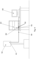
- host computer validation may be improved as any thermal tests which may be required are simplified by allowing the optical module to be located outside of the thermal chamber as illustrated in Figure 3 .
- thermal chamber tests at different thermal conditions may be performed with different optical modules plugged in.
- the thermal chamber would have to be opened and closed to change the optical modules plugged into the host computer.
- the optical module 102 may be plugged into the emulator controller 105 located outside of the thermal chamber 300.
- An electrical cable 104 may then connect the optical module 102 to the optical module emulator 101 which may then be plugged into the host computer 103 inside the thermal chamber 300. Therefore, to change the optical modules it may no longer be necessary to open and close the thermal chamber.
- the optical module may then be connected to an optical instrument 301 by an optical fiber 302.
- a controller graphical interface 303 may then monitor the performance of the host computer under different thermal conditions.
- exporting the optical module control interface to the emulator controller allows the emulator controller to analyze the control interface at a much faster frequency rate when compared to previous solutions which may have used an I2C connection to emulate the control interface.
- control channel between the controller and the emulator allows for the implementation of more complex functionality at the emulator.
- the emulator may perform power consumption emulation and timing emulation, making the emulator debug capabilities flexible for future needs.
- Embodiments described herein also avoid the need for electrical traffic cable customizations.
- electrical cables may have to be customized in order to allow for the transmission of so many signals.
- a further implementation of the embodiments described herein is for use in analysis of the control interface for newly developed optical modules, as illustrated in Figure 4 .
- the signals transmitted between the optical module and the host computer may be sampled at high frequency and by multiplexed in a specific order on a serial data stream (one per direction). These serial data streams may be transmitted along an electrical cable 104 connecting the two devices, the emulator controller 105 and the optical module emulator 101.
- a multi-frame alignment word (MFAW) comprising a sequence of multi-frame alignment bits may then be used to allow the device on the other end of the electrical cable to de-multiplex the signals and regenerate the optical module interface signals in a transparent manner.
- Figure 5 illustrates a method, in an emulator controller for obtaining a plurality of upstream signals for transmission to an optical module.
- the emulator controller receives, from an optical module emulator, a first serial data stream comprising the plurality of upstream signals multiplexed into a plurality of bits.
- the first data stream may therefore comprise sampled upstream control interface signals originating from the optical module emulator.
- these upstream control interface signals may comprise a control interface between the emulator and the emulator controller, or may comprise a control interface between the host computer and the optical module.
- the plurality of upstream signals comprise two or more of the following: serial control data transmitted from the host computer to the optical module; a serial control clock transmitted from the host computer to the optical module; serial control data transmitted between the optical module emulator to the emulator controller; a serial control clock transmitted between the optical module emulator and the emulator controller; and control signals transmitted from the host computer to the optical module.
- the first data stream therefore comprises a plurality of frames, each frame comprising a multi-frame alignment bit.
- the emulator controller then de-multiplexes, in step 502, the plurality of upstream signals based on the multi-frame alignment bit within each frame.
- Each multi-frame alignment bit comprises a bit from a predetermined multi-frame alignment word, MFAW, wherein the predetermined MFAW comprises a sequence of N bits, as described in more detail with reference to Figure 7 .
- Figure 6 illustrates a method in an optical module emulator, for obtaining a plurality of downstream signals transmitted by an emulator controller.
- the optical module emulator receives from an emulator controller, a second serial data stream comprising the plurality of downstream signals multiplexed into a plurality of bits.
- the second data stream may therefore comprise sampled downstream control interface signals originating from the emulator controller.
- these downstream control interface signals may comprise a control interface between the emulator controller and the optical module emulator, or may comprise a control interface between the optical module and the host computer.
- the plurality of downstream signals comprise one or more of the following: serial control data transmitted from the optical module to the host computer; a serial control clock transmitted from the optical module the host computer; serial control data transmitted between the emulator controller to the optical module emulator; a serial control clock transmitted between the emulator controller and the optical module emulator; and control signals transmitted from the optical module to the host computer.
- the second serial data stream comprises a plurality of frames, each frame comprising a multi-frame alignment bit.
- the optical module emulator then de-multiplexes, in step 602, the plurality of downstream signals based on the multi-frame alignment bit within each frame.
- Each multi-frame alignment bit comprises a bit from a predetermined multi-frame alignment word, MFAW, wherein the predetermined MFAW comprises a sequence of N bits, as described in more detail with reference to Figure 7 .
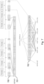
- Figure 7 illustrates an example of a protocol for the transmission of a plurality of upstream or downstream signals between an optical module emulator and an emulator controller.
- the signals which may be required to be transmitted between the optical module emulator and the emulator controller may comprise: control interface signals between the host computer and the optical module, this may include a control clock (SDA) and a control data (SDA) signal; control signals from the host computer to the optical module, (in some examples this may comprise up to 3 signals); control signals from the optical module to the host computer (in some examples this may comprise up to 3 signals); the control interface signals between the emulator controller and the optical module emulator, this may include a control clock (SCL) and a control data (SDA) signal; control signals between the emulator controller and the optical module emulator (in some examples this may comprise up to 2 signals); and control signals between the optical module emulator and the emulator controller (in some examples this may comprise up to 2 signals).
- SDA control clock
- SDA control data
- a control interface signal may be sampled multiple times per frame in order to limit as much as possible the delay introduced by the multiplexing and de-multiplexing in both directions.
- a frame may comprise M bits, comprising a sequence of interleaved samples of control signals and control interface signals.
- Each bit has a position with the frame, and this position within the frame may be illustrated by the bit number within the frame, as shown by the numbered bits 700 in figure 7 .
- position M-1 is the final bit within each frame
- position 0 is the first bit within each frame.
- each frame comprises 30 bits.
- a predetermined position within each frame is populated by a multi-frame alignment bit from a MFAW.
- the optical module emulator or emulator controller locates the MFAW within the first serial data stream or second serial data stream respectively, and from the predetermined position within each frame that the MFAW populates, determine the position of the bits of the frames within the respective first and second serial data streams.
- the MFAW 701 comprises a predetermined sequence of N bits as follows: 1011001110001111000011110000111000110010. Therefore in this example, N, the number of bits in the MFAW, is equal to 40.
- each of these multi-frame alignment bits populates a predetermined position in each frame, which, in the example illustrated in Figure 7 is position 0. Therefore the first bit of the first frame is 1, the first bit of the second frame is 0, the first bit of the third frame is 1, and so on for every bit of the MFAW.
- Each consecutive group of 40 frames may repeat this pattern with the predetermined position in each frame comprising a multi-frame alignment bit.
- each multi-frame alignment bit from the MFAW populates the first bit in each frame, i.e. position 0.
- the multi-frame alignment bit may populate any position within each frame.
- each multi-frame alignment bit may populate a different position within each frame.
- the predetermined position populated by each bit of the MFAW may be known by both the optical module emulator and the emulator controller. In this way, the emulator controller may locate the MFAW in the first serial data stream, and the optical module emulator may locate the MFAW in the second serial data stream. It will be appreciated that in some embodiments different MFAWs may be used for the upstream and downstream directions. By locating the MFAW in a data stream the optical module emulator or emulator controller determines the positions of the bits of the frames within the received data stream, and therefore de-multiplexes the received signals correctly.
- Figure 7 illustrates an example frame 702 which illustrates the multiplexing of the control interface and control signals into a single frame.
- the signals in the downstream emulator controller to optical module emulator direction may be interleaved as follows: Bit 0 may be the downstream multi-frame alignment bit, bits 1, 6, 11, 16, 21 and 26 may be the sampled optical module to host computer control data, bits 2, 7, 12, 17, 22 and 27 may be the sampled optical module to host computer control clock; bits 3, 8, 13, 18, 23, 28 may be the sampled emulator controller to optical module emulator control data; bits 4, 9, 14, 19, 24, 29 may be the sampled emulator controller to optical module emulator control clock; and bits 5, 10, 15, 20, 25 may be the optical module to host computer control signals.
- bits 1 may be the upstream multi-frame alignment bit
- bits 1, 6, 11, 16, 21 and 26 may be the sampled host computer to optical module control data
- bits 2, 7, 12, 17, 22 and 27 may be the sampled host computer optical module control clock
- bits 3, 8, 13, 18, 23, 28 may be the sampled optical module emulator to emulator controller control data
- bits 4, 9, 14, 19, 24, 29 may be the sampled optical module emulator to emulator controller control clock
- bits 5, 10, 15, 20, 25 may be the host computer to optical module control signals.
- the signals, and the multi-frame alignment bit may be interleaved within a frame in any suitable manner.
- the positions which each signal populates within a frame may be known to the emulator controller and to the optical module emulator.
- the upstream signals and downstream signals may be multiplexed in a different manner.
- each of the control interface signals is sampled 6 times per frame in order to compensate for the delay caused by multiplexing and de-multiplexing the signals.
- a frame may comprise a plurality of samples of a particular control interface signal.
- the protocol may also comprise including at least one parity bit in each frame.
- each frame comprises one parity bit every 5 bits, wherein each parity bit reports the parity of the bits between one parity bit and the following one, for example the parity of the preceding 5 bits. These parity bits may then be used for bit error detection and to avoid unwanted glitches in the de-multiplexed signals.
- the parity bits may be distributed evenly over each frame, which introduces a deterministic latency in the multiplexing/de-multiplexing of the signals.
- the emulator controller acts as the protocol master, providing the optical module emulator with a system clock and transferring all the information in the downstream direction in form of a second serial data stream.
- the optical module emulator may then use the system clock to extract the downstream signals received from the emulator controller over in the second serial data stream, recognizing the positions of the bits of the frames in the second serial data stream by locating the multi-frame alignment word (MFAW), which, in this example, comprises 1 bit per frame and repeats every N frames (see example in Figure 7 , where for instance N is equal to 40).
- MFAW multi-frame alignment word
- Figure 8 illustrates an example of a method performed by an emulator controller according to some embodiments.
- the emulator controller may first transmit a control system clock to the optical module emulator in step 802.
- the optical module emulator upon receiving the system clock, may re-transmit the control system clock back to the emulator controller, to confirm that it is present.
- the emulator controller may unlock the optical module emulator, in step 803, and may wait a predetermined slave unlock time in order for the optical module emulator to be ready to receive a second data stream. During this time, further transmissions may not be made by the emulator controller, and the state value TX may be set to 0.
- the emulator controller may enter a reset state RX RESET, in step 804, which sets an internal signal RX RESET to 1.
- the internal signal RX RESET being set to 1 forces a receive buffer which configured to store incoming data received from the optical module emulator into a reset state RX RESET in step 811.
- the resetting of the receive buffer may clear the receive buffer ready for receiving any information from the optical module emulator.
- the internal signal RX RESET is set to 1, which causes the receive buffer to reset.
- the emulator controller is configured to start writing to the receive buffer.
- the internal signal RX OK which switches to 1 when a toggle is received on an upstream data stream, is set to 0 when the receive buffer is reset in step 811.
- this receive buffer allows for resampling the receive first serial data stream from the optical module emulator using the emulator controller system clock, whilst ensuring enough of a setup/hold margin despite the different phase relationships between optical module system clock and the emulator controller system clock, which are identical but for a phase relationship which may be caused by a round trip delay time in transmitting the system clock to the optical module emulator over the electrical cable.
- the emulator controller may then start transmitting, in step 805, the MFAW to the optical module emulator.
- the state value TX may be set to MFAW.
- the emulator controller may transmit the MFAW in a second data stream to the optical module emulator by populating the predetermined position in each of N frames with consecutive bits of the MFAW. Initially, the remaining bits in each frame which are not populated by a multi-frame alignment bit may be all set to either 1 or 0. In this example therefore, the emulator controller may not commence transmitting the downstream data signals until it has confirmation that the optical module emulator has located the MFAW in the second serial data stream. As only the MFAW bits are transmitted at this stage, this means that, during hardware debugging, the MFAW pattern may be easily recognized by probing the first data stream with an oscilloscope.
- all bits not populated by one of the sequence of N bits in the second serial data stream have a value of 1.
- all bits in not populated by one of the sequence of N bits in the second data stream have a value of 0.
- the internal signal RX RESET is set to 0 and the buffer may start to write the received upstream data to the receive buffer in step 806.
- the receive buffer which runs in an upstream clock domain after a reset in step 811, starts writing at address 0 until a bit causing a toggle on the first serial data stream is received.
- the internal signal RX_OK is set to 1 and the receive buffer increases the write address for next write.
- a datavalid flag may be toggled in another ring buffer that is the same size of receive buffer.
- the emulator controller may check the datavalid flag each time a received data bit is read, so that if upstream clock stops, the datavalid flag may not be updated and the emulator controller may set an internal signal RX_DATA_ERROR to 1, forcing the emulator controller into the IDLE state in step 800.
- the emulator controller may also be set to prepare to read from the receive buffer using the downstream clock by setting the internal signal START READ to 1. However, the emulator controller may not commence reading from the receive buffer until the internal signal RX OK has been set to 1. In other words, the emulator controller may only start reading from the receive buffer once a toggle has been received on the first serial data stream from the optical module emulator. RX OK may be resampled using the downstream clock to ensure a delay between the writing and reading of the receive buffer. As described above, at each read from the receive buffer the emulator controller may also check a datavalid flag in another ring buffer, and if the datavalid flag is not updated an internal signal RX_DATA_ERROR may be set to 1, forcing the emulator controller into IDLE state in step 800.
- the emulator controller may attempt to locate a MFAW in the first serial data stream. For example, the emulator controller may receive a first bit causing a toggle on the first serial data stream from the optical module emulator. This means that the optical module emulator is sending information to the emulator controller.
- the first serial data stream may have previously comprised all 0's, and a 1 is received, or the first data stream had previously comprised all 1's, and a 0 is received.
- the emulator controller may then set the internal signal RX OK to 1 and may commence reading from the receive buffer in step 808.
- the emulator controller may then check that the first serial data stream comprises a correct MFAW in step 807. To do this, the emulator controller may set the bit which caused the toggle as the first bit of the MFAW in a first frame of N consecutive frames. The position of this first bit of the MFAW within the first frame may be set as the predetermined position within the first frame. The emulator controller may then determine whether bits populating the predetermined position in the following N-1 consecutive frames of the first serial data stream match the sequence of N bits in the MFAW.
- the emulator controller may set the bit causing the toggle as the first bit of frame 0, and may check that the first bit of the following 39 frames matches the corresponding bit of the 40 bit MFAW.
- the emulator controller may determine that it has received a correct MFAW may move to step 809. If one of the bits populating the predetermined position within the following N-1 consecutive frames of the first serial data stream does not match the MFAW, the method may return to IDLE mode in step 800. Retuning to IDLE mode may set the internal signal START READ to 0. Returning to IDLE mode may also comprise repeating the step of locating the MFAW.
- the emulator controller may continue to check further frames in the first serial data stream to check that more MFAWs are received correctly in step 809. For example, in some embodiments the emulator controller may check to receive X further correct MFAWs in step 809, where X is an integer number. In some examples X may be 4. It will be appreciated that in some embodiments X may be 0. In other words, it may not be required that the emulator controller wait to receive any further correct MFAWs.
- the method may return to IDLE mode in step 800.
- ENABLE may be set to 1
- the process may automatically restart when the method returns to IDLE mode in step 800.
- the emulator controller may determine that the optical module emulator has received a correct MFAW in the second data stream, and may therefore determine that the optical module emulator is ready to receive downstream signals. Therefore, in step 810, the value TX may be set to all bits, and the emulator controller may start transmitting the downstream signals to the optical module emulator multiplexed with the multi-frame alignment bits as illustrated in Figure 7 .
- the emulator controller may sample the plurality of downstream signals, and multiplex the plurality downstream signals such that each sample populates a bit in the second serial data stream.
- the emulator controller is now also locked onto the phase of the first serial data stream received form the optical module emulator, in step 810, and may therefore commence de-multiplexing the upstream signals according to a protocol, for example as illustrated in Figure 7 .
- the emulator controller may then, in some examples, transmit the de-multiplexed upstream signals to an optical module.
- Figure 9 illustrates a method, in an optical module emulator according to some embodiments.
- the optical module emulator may first receive a control system clock from the emulator controller, and may transmit a re-transmission of the control system clock back to the emulator controller to confirm to the emulator control that the optical module emulator is present.
- the optical module emulator may then start in IDLE mode, in step 900, and may proceed to step 901.
- the optical module emulator may be transmitting in the first serial data stream all 0's or all 1's until it locates a MFAW in the second serial data stream transmitted downstream from the emulator controller.
- a state value TX is therefore set to 0, indicating that no information is being transmitted in the first serial data stream.
- step 901 the optical module emulator starts receiving information on the second serial data stream and starts to attempt to locate a MFAW in the second serial data stream.
- the optical module emulator may be configured to locate the predetermined MFAW by setting a candidate for a multi-frame alignment bit as the first bit of the MFAW in a first frame of N consecutive frames. The optical module emulator may then set the position of the first bit as the predetermined position within the first frame; and may determine whether bits populating the predetermined position in a following N-1 consecutive frames of the second serial data stream match the sequence of N bits.
- the optical module emulator may place the candidate for a multi-frame alignment bit and all subsequent bits populating the predetermined position of the following consecutive N-1 frames into a shift register N bits wide.
- This shift register may be compared with the expected predetermined MFAW. If the bits in the shift register do not match the predetermined MFAW, the shift register may be shifted along one bit, and a new bit populates the end of the shift register. The new bit may be taken from the predetermined position in the N th frame of the second serial data stream. The shift register may then be compared to the MFAW again. This process may be repeated until the shift register matches the predetermine MFAW.
- this process may be repeated up to 2*N times, such that if the candidate for a multi-frame alignment bit was from a frame that was not the first of the multi-frames comprising a complete MFAW, the MFAW may still be located by repeating the process of shifting the shift register 2*N times. If the optical module emulator is unable to locate a MFAW, the optical module emulator may return to IDLE mode.
- the optical module emulator may determine that a correct MFAW has been received in the second serial data stream.
- the method may pass to step 902 in which the optical module emulator checks the second serial data stream for further MFAWs.
- the optical module emulator may be required to receive X consecutive MFAWs before transmitting upstream signals to the emulator controller in step 903.
- the method may pass back to IDLE mode in step 900.
- the method may pass to step 903 in which the optical module emulator may start transmitting upstream signals multiplexed into a first serial data stream with a MFAW, for example as illustrated in Figure 7 .
- the optical module emulator locates the predetermined MFAW by determining that a correct MFAW has been received in the second serial data stream before transmitting the first serial data stream to the emulator controller.
- the optical module emulator may generate a first serial data stream comprising a plurality of upstream signals; wherein the first data stream comprises plurality of frames.
- the optical module emulator may position, in the first serial data stream, predetermined multi-frame alignment bits in each respective frame; sample a plurality of upstream signals to be transmitted to the emulator controller; multiplex the sampled plurality of upstream signals into remaining bits of first serial data stream; and transmit the first serial data stream to the emulator controller.
- control interface and the control signals between the optical module emulator and the emulator controller may be transferred in real time, being multiplexed at the system clock rate at one side and de-multiplexed at the same rate at the other.
- the controller may be configured to stop transmitting downstream data for a while (to force the emulator to unlock as well), which may start the alignment process from the beginning.
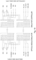
- Figure 10 illustrates an example for an SFP/SFP+/SFP28 type optical module emulator implementation for transmitting control interface and control signals between a host and an optical module.
- the control interface signals transmitted by the optical module emulator to the emulator controller comprise the signals SDA and SCL.
- the control signals transmitted by the optical module emulator to the emulator controller comprise for example, the control signals TX_DISABLE which turns off the transmitter laser output, RS0 which may be an input hardware pin which optionally selects the optical receive data path rate coverage for an SFP+ module, and RS1 which may be an input hardware pin which optionally selects the optical transmit path data rate coverage for an SFP+ module.
- the control interface received at the emulator and transmitted by the emulator controller comprises the signals SDA and SCL.
- the control signals received from the emulator controller comprise for example, the signals RX_LOS which when high may indicate an optical signal level below that specified in a relevant standard, TX_FAULT which is a module output pin that when high, indicates that the module transmitter has detected a fault condition related to laser operation or safety, and MOD_ABS which may be "High" when the SFP+ optical module is physically absent from a host slot.
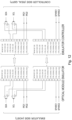
- Figure 11 illustrates an example for a QSFP/QSFP28 type optical module emulator implementation for transmitting control interface and control signals between a host and an optical module.
- the control interface signals transmitted by the optical module emulator to the emulator controller comprise the signals SDA and SCL.
- the control signals transmitted by the optical module emulator to the emulator controller comprise for example, the control signals MODESELL which when held low by the host may cause the optical module to respond to 2-wire serial communication commands, RESETL which enables a complete reset by returning the settings to their default state when a low level on the RESETL pin is held for longer than a minimum pulse length, and LPMODE which may be used to set the maximum power consumption for the optical module in order to protect hosts that are not capable of cooling higher power optical modules.
- the control interface received at the optical module emulator and transmitted by the emulator controller comprises the signals SDA and SCL.
- the control signals received at the optical module emulator from the emulator controller may comprise for example, the signals MODPRESL which when high may indicate that an optical module is not present, and INT_L which when low may indicate a possible operational fault or a status critical to the host system.
- Figure 12 illustrates an example for control channel implementation for controlling the optical module emulator.
- the control interface signals transmitted by the optical module emulator to the emulator controller comprise the signals SDA and SCL.
- the control signals transmitted by the optical module emulator to the emulator controller comprise for example, interrupt requests IRQ1 and IRQ2.
- the control interface received at the optical module emulator and transmitted by the emulator controller comprises the signals SDA and SCL.
- the control signals received at the optical module emulator from the emulator controller may comprise for example, control signals SPARE1 and SPARE2 which may be used to provide any form of control to the optical module emulator.
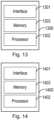
- FIG. 13 illustrates an example of an emulator controller 1300 according to some embodiments.
- the emulator controller 1300 comprises an interface 1301, a processor 1302 and a memory 1303.
- the processor may be any type of processor, e.g. integrated circuitry or processing circuitry, e.g. in form of an FPGA (Field Programmable Gate Array) and/or ASIC (Application Specific Integrated Circuitry).
- the processor may be configured to receive, from an optical module emulator, a first serial data stream comprising the plurality of upstream signals multiplexed into a plurality of bits; wherein the first data stream comprises a plurality of frames, each frame comprising a multi-frame alignment bit.
- the processor 1302 may be further configured to de-multiplex the plurality of upstream signals based on each multi-frame alignment bit within each respective frame. In some embodiments it will be appreciated that the processor 1302 may be configured to perform a method such as the method illustrated in Figure 8 .
- the memory 1303 may comprise a receive buffer as described in Figure 8 .
- the memory 1303 may also comprise the predetermined MFAW.
- FIG 14 illustrates an example of an optical module emulator 1400 according to some embodiments.
- the optical module emulator 1400 comprises an interface 1401, a processor 1402 and a memory 1403.
- the processor 1402 may be configured to receive, from the emulator controller, a second serial data stream comprising the plurality of downstream signals multiplexed into a plurality of bits; wherein the second serial data stream comprises a plurality of frames, each frame comprising a multi-frame alignment bit.
- the processor 1402 may be further configured to de-multiplex the plurality of downstream signals based on each multi-frame alignment bit within each respective frame.
- the processor 1402 may be configured to perform a method such as the method illustrated in Figure 9 .
- the memory 1403 may comprise the predetermined MFAW.
- the emulator controller or optical module emulator may be considered as a plurality of units or modules.
- the units or modules may be implemented with a processor 1402, and optionally memory 1403.
- the units or modules may be functional units or modules, and may for example be implemented in an integrated circuit.
- the emulator controller 1300 or optical module emulator 1400 are for obtaining a plurality of upstream or downstream signals for transmission to, or reception from, an optical module.
- the emulator controller may comprise a receiving module configured to receive from an optical module emulator a first serial data stream comprising the plurality of upstream signals multiplexed into a plurality of bits.
- the first data stream comprises a plurality of frames, each frame comprising a multi-frame alignment bit.
- the emulator controller further comprises a de-multiplexing module configured to de-multiplex the plurality of upstream signals based on each multi-frame alignment bit within each respective frame.
- the optical module emulator may comprise a receiving module configured to receive from an emulator controller a second serial data stream comprising a plurality of downstream signals multiplexed into a plurality of bits.
- the second serial data stream comprises a plurality of frames, each frame comprising a multi-frame alignment bit.
- the optical module emulator further comprises a de-multiplexing module configured to de-multiplex the plurality of downstream signals based on each multi-frame alignment bit within each respective frame.
Landscapes
- Engineering & Computer Science (AREA)
- Computer Networks & Wireless Communication (AREA)
- Signal Processing (AREA)
- Physics & Mathematics (AREA)
- Electromagnetism (AREA)
- General Physics & Mathematics (AREA)
- Optics & Photonics (AREA)
- Optical Communication System (AREA)
- Information Transfer Systems (AREA)
Claims (15)
- Verfahren in einer Emulatorsteuerung zum Erhalten einer Vielzahl von Upstream-Signalen für eine Übertragung an ein optisches Modul, wobei die Emulatorsteuerung eine Steuerschnittstelle und Steuersignale für ein optisches Modul überwacht, das Verfahren umfassend:Empfangen (501), von einem entfernten optischen Modulemulator, eines ersten seriellen Datenstroms, umfassend die Vielzahl von Upstream-Signalen, die in eine Vielzahl von Bits gemultiplext sind; wobei der erste Datenstrom eine Vielzahl von Frames umfasst, jeder Frame umfassend ein Multi-Frame-Synchronisierbit, wobei jedes Multi-Frame-Synchronisierbit ein Bit aus einem zuvor bestimmten Multi-Frame-Synchronisierwort, MFAW, umfasst, wobei das zuvor bestimmte MFAW eine Sequenz von N Bits umfasst; undDemultiplexen (502) der Vielzahl von Upstream-Signalen basierend auf jedem Multi-Frame-Synchronisierbit innerhalb jedes jeweiligen Frames;Lokalisieren, in dem ersten seriellen Datenstrom, des zuvor bestimmten MFAW; wobei jedes Multi-Frame-Synchronisierbit eine zuvor bestimmte Position innerhalb eines der Vielzahl von Frames befüllt, wobei der Schritt des Lokalisierens umfasst;Empfangen eines ersten Bits, das ein Umschalten in dem ersten seriellen Datenstrom verursacht;Festlegen des ersten Bits als ein erstes Bit des MFAW in einem ersten Frame von N aufeinanderfolgenden Frames,Festlegen der Position des ersten Bits als die zuvor bestimmte Position innerhalb des ersten Frames; undBestimmen, ob Bits, die die zuvor bestimmte Position in einem folgenden N-1 aufeinanderfolgenden Frames des ersten seriellen Datenstroms befüllen, mit der Sequenz von N Bits übereinstimmen.
- Verfahren nach Anspruch 1, ferner umfassend, als Reaktion auf eine Bestimmung, dass die Bits, die die zuvor bestimmte Position innerhalb der folgenden N-1 aufeinanderfolgenden Frames des ersten seriellen Datenstroms befüllen, mit der Sequenz von N Bits übereinstimmen, Bestimmen, dass ein korrektes MFAW empfangen wurde.
- Verfahren nach Anspruch 1 oder 2, ferner umfassend, als Reaktion auf eine Bestimmung, dass die Bits, die die zuvor bestimmte Position in den folgenden N-1 aufeinanderfolgenden Frames des ersten Datenstroms befüllen, nicht mit der Sequenz von N Bits übereinstimmen, ein Wiederholen des Schritts zum Lokalisieren des MFAW.
- Verfahren nach einem der vorstehenden Ansprüche, ferner umfassend zunächst das Übertragen eines Steuersystemtakts an den optischen Modulemulator; undEmpfangen einer erneuten Übertragung des Steuersystemtakts von dem optischen Modulemulator; und optional,wobei die Vielzahl von Upstream-Signalen eine Steuerschnittstelle und/oder mindestens ein Steuersignal umfasst.
- Verfahren nach Anspruch 4, wobei jeder Frame des ersten seriellen Datenstroms mehrere Abtastwerte der Steuerschnittstelle umfasst; und/oder wobei die Steuerschnittstelle eines oder mehrere der folgenden umfasst: serielle Steuerdaten, die von dem Host-Computer an das optische Modul übertragen werden; einen seriellen Steuertakt, der von dem Host-Computer an das optische Modul übertragen wird; serielle Steuerdaten, die zwischen dem optischen Modulemulator und der Emulatorsteuerung übertragen werden; einen seriellen Steuertakt, der zwischen dem optischen Modulemulator und der Emulatorsteuerung übertragen wird; und Steuersignale, die von dem Host-Computer an das optische Modul übertragen werden.
- Verfahren nach Anspruch 1, ferner umfassend;Übertragen, in einem zweiten Datenstrom, des MFAW an den optischen Modulemulator durch das Befüllen der zuvor bestimmten Position in jedem von N Frames mit aufeinanderfolgenden Bits des MFAW,wobei vor dem Lokalisieren des MFAW in dem ersten Datenstrom alle Bits, die nicht durch eine der Sequenzen von N Bits in dem zweiten Datenstrom befüllt sind, einen Wert von 1 aufweisen oder alle Bits, die nicht durch eine der Sequenzen von N Bits in dem zweiten Datenstrom befüllt sind, einen Wert von 0 aufweisen.
- Verfahren nach Anspruch 6, ferner umfassend:
als Reaktion auf das Lokalisieren des MFAW in dem ersten Datenstrom, Übertragen von Downstream-Signalen in dem zweiten seriellen Datenstrom, der mit dem MFAW gemultiplext ist; und optional ferner umfassend:Abtasten der Vielzahl von Downstream-Signalen; undderartiges Multiplexen der Vielzahl von Downstream-Signalen, dass jeder Abtastwert ein Bit in dem zweiten seriellen Datenstrom befüllt. - Verfahren in einem optischen Modulemulator zum Erhalten einer Vielzahl von Downstream-Signalen, die durch eine entfernte Emulatorsteuerung übertragen werden, das Verfahren umfassend:Empfangen (601) von der entfernten Emulatorsteuerung eines zweiten seriellen Datenstroms, umfassend die Vielzahl von Downstream-Signalen, die in eine Vielzahl von Bits gemultiplext sind; wobei der zweite serielle Datenstrom eine Vielzahl von Frames umfasst, jeder Frame umfassend ein Multi-Frame-Synchronisierbit, wobei jedes Multi-Frame-Synchronisierbit ein Bit aus einem zuvor bestimmten Multi-Frame-Synchronisierwort, MFAW, umfasst, wobei das zuvor bestimmte MFAW eine Sequenz von N Bits umfasst; undDemultiplexen (602) der Vielzahl von Downstream-Signalen basierend auf jedem Multi-Frame-Synchronisierbit innerhalb jedes jeweiligen Frames;Lokalisieren, in dem zweiten seriellen Datenstrom, des zuvor bestimmten MFAW; wobei jedes Multi-Frame-Synchronisierbit eine zuvor bestimmte Position innerhalb eines der Vielzahl von Frames befüllt, wobei der Schritt des Lokalisierens umfasst:Empfangen eines Kandidaten-Multi-Frame-Synchronisierbits;Festlegen des Kandidaten-Multi-Frame-Synchronisierbits als ein erstes Bit des MFAW in einem ersten Frame von N aufeinanderfolgenden Frames,Festlegen der Position des ersten Bits als die zuvor bestimmte Position innerhalb des ersten Frames; undBestimmen, ob Bits, die die zuvor bestimmte Position in einem folgenden N-1 aufeinanderfolgenden Frames des zweiten seriellen Datenstroms befüllen, mit der Sequenz von N Bits übereinstimmen.
- Verfahren nach Anspruch 8, wobei die Vielzahl von Downstream-Signalen eine Steuerschnittstelle und/oder mindestens ein Steuersignal umfasst; und wobei optional jeder Frame des zweiten seriellen Datenstroms mehrere Abtastwerte der Steuerschnittstelle umfasst.
- Verfahren nach Anspruch 9, wobei die Steuerschnittstelle eines oder mehrere umfasst von: seriellen Steuerdaten, die von dem optischen Modul an den Host-Computer übertragen werden; einen seriellen Steuertakt, der von dem optischen Modul an den Host-Computer übertragen wird; serielle Steuerdaten, die zwischen der Emulatorsteuerung und dem optischen Modulemulator übertragen werden; einen seriellen Steuertakt, der zwischen der Emulatorsteuerung und dem optischen Modulemulator übertragen wird; und Steuersignale, die von dem optischen Modul an den Host-Computer übertragen werden.
- Verfahren nach Anspruch 8, ferner umfassend:Positionieren, in einem ersten seriellen Datenstrom, jeweiliger zuvor bestimmter Multi-Frame-Synchronisierbits in jedem jeweiligen Frame;Abtasten einer Vielzahl von Upstream-Signalen, die an die Emulatorsteuerung zu übertragen sind;Multiplexen der abgetasteten Vielzahl von Upstream-Signalen in verbleibende Bits des ersten seriellen Datenstroms; undÜbertragen des ersten seriellen Datenstroms an die Emulatorsteuerung.
- Verfahren nach Anspruch 8, ferner umfassend das Lokalisieren des zuvor bestimmten MFAW durch das Bestimmen, dass ein korrektes MFAW in dem zweiten seriellen Datenstrom empfangen wurde, bevor der erste Datenstrom an die Emulatorsteuerung übertragen wird.
- Verfahren nach Anspruch 12, ferner umfassend, als Reaktion auf eine Bestimmung, dass die Bits, die die zuvor bestimmte Frame-Position in den folgenden N-1 aufeinanderfolgenden Frames des zweiten seriellen Datenstroms befüllen, mit der Sequenz von N Bits übereinstimmen, Bestimmen, dass ein korrektes MFAW in dem zweiten seriellen Datenstrom empfangen wurde.
- Emulatorsteuerung (105) zum Erhalten einer Vielzahl von Upstream-Signalen für die Übertragung an ein optisches Modul, wobei die Emulatorsteuerung konfiguriert ist, um eine Steuerschnittstelle und Steuersignale für ein optisches Modul zu überwachen, die Emulatorsteuerung umfassend:eine Schnittstelle; undein Prozessor, wobei der Prozessor konfiguriert ist zum;Empfangen, von einem entfernten optischen Modulemulator, eines ersten seriellen Datenstroms, umfassend die Vielzahl von Upstream-Signalen, die in eine Vielzahl von Bits gemultiplext sind; wobei der erste Datenstrom eine Vielzahl von Frames umfasst, jeder Frame umfassend ein Multi-Frame-Synchronisierbit, wobei jedes Multi-Frame-Synchronisierbit ein Bit aus einem zuvor bestimmten Multi-Frame-Synchronisierwort, MFAW, umfasst, wobei das zuvor bestimmte MFAW eine Sequenz von N Bits umfasst; undDemultiplexen der Vielzahl von Upstream-Signalen basierend auf jedem Multi-Frame-Synchronisierbit innerhalb jedes jeweiligen Frames;Lokalisieren, in dem ersten seriellen Datenstrom, des zuvor bestimmten MFAW; wobei jedes Multi-Frame-Synchronisierbit eine zuvor bestimmte Position innerhalb eines der Vielzahl von Frames befüllt, wobei der Prozessor konfiguriert ist, um das zuvor bestimmte MFAW zu lokalisieren durch;Empfangen eines ersten Bits, das ein Umschalten in dem ersten seriellen Datenstrom verursacht;Festlegen des ersten Bits als ein erstes Bit des MFAW in einem ersten Frame von N aufeinanderfolgenden Frames,Festlegen der Position des ersten Bits als die zuvor bestimmte Position innerhalb des ersten Frames; undBestimmen, ob Bits, die die zuvor bestimmte Position in einem folgenden N-1 aufeinanderfolgenden Frames des ersten seriellen Datenstroms befüllen, mit der Sequenz von N Bits übereinstimmen.
- Optischer Modulemulator (101) zum Erhalten einer Vielzahl von Downstream-Signalen, die durch eine entfernte Emulatorsteuerung übertragen werden, der optische Modulemulator umfassend:eine Schnittstelle; undeinen Prozessor, wobei der Prozessor konfiguriert ist zum:Empfangen, von der entfernten Emulatorsteuerung, eines zweiten seriellen Datenstroms, umfassend die Vielzahl von Downstream-Signalen, die in eine Vielzahl von Bits gemultiplext sind; wobei der zweite serielle Datenstrom eine Vielzahl von Frames umfasst, jeder Frame umfassend ein Multi-Frame-Synchronisierbit, wobei jedes Multi-Frame-Synchronisierbit ein Bit aus einem zuvor bestimmten Multi-Frame-Synchronisierwort, MFAW, umfasst, wobei das zuvor bestimmte MFAW eine Sequenz von N Bits umfasst; undDemultiplexen der Vielzahl von Downstream-Signalen basierend auf jedem Multi-Frame-Synchronisierbit innerhalb jedes jeweiligen Frames;Lokalisieren, in dem zweiten seriellen Datenstrom, des zuvor bestimmten MFAW; wobei jedes Multi-Frame-Synchronisierbit eine zuvor bestimmte Position innerhalb eines der Vielzahl von Frames befüllt, wobei der Prozessor konfiguriert ist, um das zuvor bestimmte MFAW zu lokalisieren durch:Empfangen eines Kandidaten-Multi-Frame-Synchronisierbits;Festlegen des Kandidaten-Multi-Frame-Synchronisierbits als ein erstes Bit des MFAW in einem ersten Frame von N aufeinanderfolgenden Frames,Festlegen der Position des ersten Bits als die zuvor bestimmte Position innerhalb des ersten Frames; undBestimmen, ob Bits, die die zuvor bestimmte Position in einem folgenden N-1 aufeinanderfolgenden Frames des zweiten seriellen Datenstroms befüllen, mit der Sequenz von N Bits übereinstimmen.
Applications Claiming Priority (1)
| Application Number | Priority Date | Filing Date | Title |
|---|---|---|---|
| PCT/EP2017/084216 WO2019120552A1 (en) | 2017-12-21 | 2017-12-21 | Methods and apparatus for providing emulation of optical modules |
Publications (2)
| Publication Number | Publication Date |
|---|---|
| EP3729690A1 EP3729690A1 (de) | 2020-10-28 |
| EP3729690B1 true EP3729690B1 (de) | 2025-02-19 |
Family
ID=60957289
Family Applications (1)
| Application Number | Title | Priority Date | Filing Date |
|---|---|---|---|
| EP17828912.0A Active EP3729690B1 (de) | 2017-12-21 | 2017-12-21 | Verfahren und vorrichtung zur bereitstellung der emulation von optischen modulen |
Country Status (3)
| Country | Link |
|---|---|
| US (1) | US11528083B2 (de) |
| EP (1) | EP3729690B1 (de) |
| WO (1) | WO2019120552A1 (de) |
Family Cites Families (6)
| Publication number | Priority date | Publication date | Assignee | Title |
|---|---|---|---|---|
| AU2001274937A1 (en) * | 2000-05-24 | 2001-12-03 | Purdue Research Foundation | Methods and systems for polarization control and polarization mode dispersion compensation for wideband optical signals |
| US6807523B1 (en) * | 2001-10-31 | 2004-10-19 | Ciena Corporation | Method and apparatus for emulating the optical behavior of optical communication systems |
| US7890821B2 (en) * | 2007-10-04 | 2011-02-15 | Veriwave, Inc. | Channel impairment emulator systems and methods |
| JP2009200585A (ja) * | 2008-02-19 | 2009-09-03 | Nec Corp | 光送受信装置、その通信方法、及び通信システム |
| US20150349906A1 (en) * | 2014-05-30 | 2015-12-03 | Eric Joseph Christensen | Scalable efficient framing for digital signals |
| US9497522B2 (en) * | 2014-08-19 | 2016-11-15 | Ciena Corporation | Flexible smart sleeve systems and methods for pluggable transceivers |
-
2017
- 2017-12-21 US US16/954,877 patent/US11528083B2/en active Active
- 2017-12-21 EP EP17828912.0A patent/EP3729690B1/de active Active
- 2017-12-21 WO PCT/EP2017/084216 patent/WO2019120552A1/en not_active Ceased
Also Published As
| Publication number | Publication date |
|---|---|
| US20200403719A1 (en) | 2020-12-24 |
| US11528083B2 (en) | 2022-12-13 |
| EP3729690A1 (de) | 2020-10-28 |
| WO2019120552A1 (en) | 2019-06-27 |
Similar Documents
| Publication | Publication Date | Title |
|---|---|---|
| EP2609697B1 (de) | Skalierbare aktive gigabit-hochgeschwindigkeitsbündelverbindung und tester | |
| EP2773068B1 (de) | Testvorrichtung und Verfahren | |
| CN109558371B (zh) | 用于与微控制器通信的方法、以及计算系统 | |
| CN107704346B (zh) | Soc芯片调试方法及调试系统 | |
| JP6427500B2 (ja) | 多数のデータパケット信号送受信機を同時に試験する方法 | |
| EP2628087B1 (de) | Verfahren und systeme zum testen des elektrischen verhaltens einer verbindung mit asymmetrischen verknüpfungen | |
| CN107025203B (zh) | 第一板卡、第二板卡及一种设备 | |
| CN102972070A (zh) | 使用多网络地址来建立被测设备和控制测试的测试设备的同步的系统和方法 | |
| US20170337152A1 (en) | Port mirroring for peripheral component interconnect express devices | |
| EP4049477B1 (de) | Übertragungsratenanpassung | |
| KR101185971B1 (ko) | 통신 시스템, 시험 장치, 통신 장치, 통신 방법 및 시험 방법 | |
| EP2197218A1 (de) | Verteilte intercross-einrichtung eines gemeinsam benutzten busses | |
| CN106685588B (zh) | 一种适配器、数据传输系统及方法 | |
| CN103759760B (zh) | 测试的方法与装置 | |
| US20150033082A1 (en) | Method and Apparatus for Multi-chip Reduced Pin Cross Triggering To Enhance Debug Experience | |
| US11528083B2 (en) | Methods and apparatus for providing emulation of optical modules | |
| CN110646723B (zh) | 总线接口测试电路和方法 | |
| JP4736135B2 (ja) | カード間通信を行う内部バス解析システム、その方法及びそのプログラム | |
| CN100370765C (zh) | 测试使用光模块的单板电接口的方法及装置 | |
| US9720871B2 (en) | Determining cable connections in a multi-cable link | |
| CN109885420A (zh) | 一种PCIe链路故障的分析方法、BMC及存储介质 | |
| CN119109539A (zh) | 一种用于无线通信系统仿真测试的装置和方法 | |
| CN213461779U (zh) | 基于以太网线的时钟同步装置及系统 | |
| JP7790770B2 (ja) | リンク確立装置、方法及びシステム | |
| CN113259000B (zh) | 一种光模块测试装置 |
Legal Events
| Date | Code | Title | Description |
|---|---|---|---|
| STAA | Information on the status of an ep patent application or granted ep patent |
Free format text: STATUS: UNKNOWN |
|
| STAA | Information on the status of an ep patent application or granted ep patent |
Free format text: STATUS: THE INTERNATIONAL PUBLICATION HAS BEEN MADE |
|
| PUAI | Public reference made under article 153(3) epc to a published international application that has entered the european phase |
Free format text: ORIGINAL CODE: 0009012 |
|
| STAA | Information on the status of an ep patent application or granted ep patent |
Free format text: STATUS: REQUEST FOR EXAMINATION WAS MADE |
|
| 17P | Request for examination filed |
Effective date: 20200612 |
|
| AK | Designated contracting states |
Kind code of ref document: A1 Designated state(s): AL AT BE BG CH CY CZ DE DK EE ES FI FR GB GR HR HU IE IS IT LI LT LU LV MC MK MT NL NO PL PT RO RS SE SI SK SM TR |
|
| AX | Request for extension of the european patent |
Extension state: BA ME |
|
| DAV | Request for validation of the european patent (deleted) | ||
| DAX | Request for extension of the european patent (deleted) | ||
| STAA | Information on the status of an ep patent application or granted ep patent |
Free format text: STATUS: EXAMINATION IS IN PROGRESS |
|
| 17Q | First examination report despatched |
Effective date: 20220518 |
|
| GRAP | Despatch of communication of intention to grant a patent |
Free format text: ORIGINAL CODE: EPIDOSNIGR1 |
|
| STAA | Information on the status of an ep patent application or granted ep patent |
Free format text: STATUS: GRANT OF PATENT IS INTENDED |
|
| INTG | Intention to grant announced |
Effective date: 20240927 |
|
| GRAS | Grant fee paid |
Free format text: ORIGINAL CODE: EPIDOSNIGR3 |
|
| GRAA | (expected) grant |
Free format text: ORIGINAL CODE: 0009210 |
|
| STAA | Information on the status of an ep patent application or granted ep patent |
Free format text: STATUS: THE PATENT HAS BEEN GRANTED |
|
| AK | Designated contracting states |
Kind code of ref document: B1 Designated state(s): AL AT BE BG CH CY CZ DE DK EE ES FI FR GB GR HR HU IE IS IT LI LT LU LV MC MK MT NL NO PL PT RO RS SE SI SK SM TR |
|
| REG | Reference to a national code |
Ref country code: GB Ref legal event code: FG4D |
|
| REG | Reference to a national code |
Ref country code: CH Ref legal event code: EP |
|
| REG | Reference to a national code |
Ref country code: IE Ref legal event code: FG4D |
|
| REG | Reference to a national code |
Ref country code: DE Ref legal event code: R096 Ref document number: 602017087895 Country of ref document: DE |
|
| REG | Reference to a national code |
Ref country code: NL Ref legal event code: MP Effective date: 20250219 |
|
| PG25 | Lapsed in a contracting state [announced via postgrant information from national office to epo] |
Ref country code: RS Free format text: LAPSE BECAUSE OF FAILURE TO SUBMIT A TRANSLATION OF THE DESCRIPTION OR TO PAY THE FEE WITHIN THE PRESCRIBED TIME-LIMIT Effective date: 20250519 |
|
| PG25 | Lapsed in a contracting state [announced via postgrant information from national office to epo] |
Ref country code: FI Free format text: LAPSE BECAUSE OF FAILURE TO SUBMIT A TRANSLATION OF THE DESCRIPTION OR TO PAY THE FEE WITHIN THE PRESCRIBED TIME-LIMIT Effective date: 20250219 |
|
| PG25 | Lapsed in a contracting state [announced via postgrant information from national office to epo] |
Ref country code: PL Free format text: LAPSE BECAUSE OF FAILURE TO SUBMIT A TRANSLATION OF THE DESCRIPTION OR TO PAY THE FEE WITHIN THE PRESCRIBED TIME-LIMIT Effective date: 20250219 |
|
| PG25 | Lapsed in a contracting state [announced via postgrant information from national office to epo] |
Ref country code: ES Free format text: LAPSE BECAUSE OF FAILURE TO SUBMIT A TRANSLATION OF THE DESCRIPTION OR TO PAY THE FEE WITHIN THE PRESCRIBED TIME-LIMIT Effective date: 20250219 |
|
| REG | Reference to a national code |
Ref country code: LT Ref legal event code: MG9D |
|
| PG25 | Lapsed in a contracting state [announced via postgrant information from national office to epo] |
Ref country code: NO Free format text: LAPSE BECAUSE OF FAILURE TO SUBMIT A TRANSLATION OF THE DESCRIPTION OR TO PAY THE FEE WITHIN THE PRESCRIBED TIME-LIMIT Effective date: 20250519 Ref country code: IS Free format text: LAPSE BECAUSE OF FAILURE TO SUBMIT A TRANSLATION OF THE DESCRIPTION OR TO PAY THE FEE WITHIN THE PRESCRIBED TIME-LIMIT Effective date: 20250619 |
|
| PG25 | Lapsed in a contracting state [announced via postgrant information from national office to epo] |
Ref country code: NL Free format text: LAPSE BECAUSE OF FAILURE TO SUBMIT A TRANSLATION OF THE DESCRIPTION OR TO PAY THE FEE WITHIN THE PRESCRIBED TIME-LIMIT Effective date: 20250219 |
|
| PG25 | Lapsed in a contracting state [announced via postgrant information from national office to epo] |
Ref country code: HR Free format text: LAPSE BECAUSE OF FAILURE TO SUBMIT A TRANSLATION OF THE DESCRIPTION OR TO PAY THE FEE WITHIN THE PRESCRIBED TIME-LIMIT Effective date: 20250219 |
|
| PG25 | Lapsed in a contracting state [announced via postgrant information from national office to epo] |
Ref country code: PT Free format text: LAPSE BECAUSE OF FAILURE TO SUBMIT A TRANSLATION OF THE DESCRIPTION OR TO PAY THE FEE WITHIN THE PRESCRIBED TIME-LIMIT Effective date: 20250620 Ref country code: LV Free format text: LAPSE BECAUSE OF FAILURE TO SUBMIT A TRANSLATION OF THE DESCRIPTION OR TO PAY THE FEE WITHIN THE PRESCRIBED TIME-LIMIT Effective date: 20250219 |
|
| PG25 | Lapsed in a contracting state [announced via postgrant information from national office to epo] |
Ref country code: BG Free format text: LAPSE BECAUSE OF FAILURE TO SUBMIT A TRANSLATION OF THE DESCRIPTION OR TO PAY THE FEE WITHIN THE PRESCRIBED TIME-LIMIT Effective date: 20250219 Ref country code: GR Free format text: LAPSE BECAUSE OF FAILURE TO SUBMIT A TRANSLATION OF THE DESCRIPTION OR TO PAY THE FEE WITHIN THE PRESCRIBED TIME-LIMIT Effective date: 20250520 |
|
| REG | Reference to a national code |
Ref country code: AT Ref legal event code: MK05 Ref document number: 1769338 Country of ref document: AT Kind code of ref document: T Effective date: 20250219 |
|
| PG25 | Lapsed in a contracting state [announced via postgrant information from national office to epo] |
Ref country code: SE Free format text: LAPSE BECAUSE OF FAILURE TO SUBMIT A TRANSLATION OF THE DESCRIPTION OR TO PAY THE FEE WITHIN THE PRESCRIBED TIME-LIMIT Effective date: 20250219 |
|
| PG25 | Lapsed in a contracting state [announced via postgrant information from national office to epo] |
Ref country code: SM Free format text: LAPSE BECAUSE OF FAILURE TO SUBMIT A TRANSLATION OF THE DESCRIPTION OR TO PAY THE FEE WITHIN THE PRESCRIBED TIME-LIMIT Effective date: 20250219 |
|
| PG25 | Lapsed in a contracting state [announced via postgrant information from national office to epo] |
Ref country code: DK Free format text: LAPSE BECAUSE OF FAILURE TO SUBMIT A TRANSLATION OF THE DESCRIPTION OR TO PAY THE FEE WITHIN THE PRESCRIBED TIME-LIMIT Effective date: 20250219 |
|
| PG25 | Lapsed in a contracting state [announced via postgrant information from national office to epo] |
Ref country code: IT Free format text: LAPSE BECAUSE OF FAILURE TO SUBMIT A TRANSLATION OF THE DESCRIPTION OR TO PAY THE FEE WITHIN THE PRESCRIBED TIME-LIMIT Effective date: 20250219 |
|
| PG25 | Lapsed in a contracting state [announced via postgrant information from national office to epo] |
Ref country code: AT Free format text: LAPSE BECAUSE OF FAILURE TO SUBMIT A TRANSLATION OF THE DESCRIPTION OR TO PAY THE FEE WITHIN THE PRESCRIBED TIME-LIMIT Effective date: 20250219 |
|
| PG25 | Lapsed in a contracting state [announced via postgrant information from national office to epo] |
Ref country code: EE Free format text: LAPSE BECAUSE OF FAILURE TO SUBMIT A TRANSLATION OF THE DESCRIPTION OR TO PAY THE FEE WITHIN THE PRESCRIBED TIME-LIMIT Effective date: 20250219 Ref country code: CZ Free format text: LAPSE BECAUSE OF FAILURE TO SUBMIT A TRANSLATION OF THE DESCRIPTION OR TO PAY THE FEE WITHIN THE PRESCRIBED TIME-LIMIT Effective date: 20250219 |
|
| PG25 | Lapsed in a contracting state [announced via postgrant information from national office to epo] |
Ref country code: RO Free format text: LAPSE BECAUSE OF FAILURE TO SUBMIT A TRANSLATION OF THE DESCRIPTION OR TO PAY THE FEE WITHIN THE PRESCRIBED TIME-LIMIT Effective date: 20250219 |
|
| PG25 | Lapsed in a contracting state [announced via postgrant information from national office to epo] |
Ref country code: SK Free format text: LAPSE BECAUSE OF FAILURE TO SUBMIT A TRANSLATION OF THE DESCRIPTION OR TO PAY THE FEE WITHIN THE PRESCRIBED TIME-LIMIT Effective date: 20250219 |
|
| REG | Reference to a national code |
Ref country code: DE Ref legal event code: R097 Ref document number: 602017087895 Country of ref document: DE |
|
| PLBE | No opposition filed within time limit |
Free format text: ORIGINAL CODE: 0009261 |
|
| STAA | Information on the status of an ep patent application or granted ep patent |
Free format text: STATUS: NO OPPOSITION FILED WITHIN TIME LIMIT |
|
| PGFP | Annual fee paid to national office [announced via postgrant information from national office to epo] |
Ref country code: GB Payment date: 20251229 Year of fee payment: 9 |
|
| 26N | No opposition filed |
Effective date: 20251120 |
|
| PGFP | Annual fee paid to national office [announced via postgrant information from national office to epo] |
Ref country code: DE Payment date: 20251229 Year of fee payment: 9 |