EP3729633B1 - Schalterunterstütztes diodengeklemmtes energiesammelsystem für wandler mit variabler kapazität - Google Patents
Schalterunterstütztes diodengeklemmtes energiesammelsystem für wandler mit variabler kapazität Download PDFInfo
- Publication number
- EP3729633B1 EP3729633B1 EP18826001.2A EP18826001A EP3729633B1 EP 3729633 B1 EP3729633 B1 EP 3729633B1 EP 18826001 A EP18826001 A EP 18826001A EP 3729633 B1 EP3729633 B1 EP 3729633B1
- Authority
- EP
- European Patent Office
- Prior art keywords
- variable capacitor
- voltage
- switch
- capacitor
- conductive state
- Prior art date
- Legal status (The legal status is an assumption and is not a legal conclusion. Google has not performed a legal analysis and makes no representation as to the accuracy of the status listed.)
- Active
Links
Images



Classifications
-
- H—ELECTRICITY
- H02—GENERATION; CONVERSION OR DISTRIBUTION OF ELECTRIC POWER
- H02N—ELECTRIC MACHINES NOT OTHERWISE PROVIDED FOR
- H02N1/00—Electrostatic generators or motors using a solid moving electrostatic charge carrier
-
- H—ELECTRICITY
- H02—GENERATION; CONVERSION OR DISTRIBUTION OF ELECTRIC POWER
- H02N—ELECTRIC MACHINES NOT OTHERWISE PROVIDED FOR
- H02N2/00—Electric machines in general using piezoelectric effect, electrostriction or magnetostriction
- H02N2/18—Electric machines in general using piezoelectric effect, electrostriction or magnetostriction producing electrical output from mechanical input, e.g. generators
- H02N2/181—Circuits; Control arrangements or methods
-
- G—PHYSICS
- G01—MEASURING; TESTING
- G01R—MEASURING ELECTRIC VARIABLES; MEASURING MAGNETIC VARIABLES
- G01R19/00—Arrangements for measuring currents or voltages or for indicating presence or sign thereof
- G01R19/0046—Arrangements for measuring currents or voltages or for indicating presence or sign thereof characterised by a specific application or detail not covered by any other subgroup of G01R19/00
Definitions
- the present invention relates to an energy harvesting system for harvesting electrical energy from at least one variable capacitor. Moreover, the invention relates to a method for harvesting electrical energy from at least one variable capacitor using such an energy harvesting system.
- WO 2010/146457 discloses an environmental electrical generator having variable capacitors that each includes a repeatedly stretched and relaxed sheet of stretchable material and electrodes lying against opposite faces of the sheet, which includes a power extraction unit coupled to the electrodes of at least a pair of capacitors.
- the unit directs an electrical charge (current) from a first pair of electrodes that have a higher voltage, to one or more second pairs of electrodes that have a lower voltage, to recharge the second pairs of electrodes.
- electrical power is extracted by the drop-in voltage of current passing through the unit.
- the power extraction unit can be provided with a control unit that has voltage detectors and that selectively connect capacitors, based on their voltages, for maximum efficiency in generating power output.
- variable capacitor connects to a half-bridge consisting of a pair of anti-parallel diodes, which creates a passive harvesting system in which the charging and discharging cycle follows the change of the capacitance of the variable capacitor e.g., as induced by a changing external force acting on the variable capacitor.
- a description of this energy harvesting system has been published in: R. van Kessel, A. Wattez, and P. Bauer, "Analyses and comparison of an energy harvesting system for dielectric elastomer generators using a passive harvesting concept: the voltage-clamped multi-phase system," in SS/NDE 2015 - Electroactive Polymer Actuators and Devices (EAPAD) XVII, ser. Proc.
- the system comprises two voltage sources in series, diode half-bridges connected in parallel with the first voltage source, and each variable capacitor connected between the common node of the respective half-bridge and the opposite polarity terminal of the second voltage source.
- the energy harvesting system of the prior art has a relatively low energy capture ability, especially for small capacitance variation levels. As a result it has a low efficiency at particularly small capacitance variation levels due to dielectric losses which are roughly constant and independent of the capacitance variation.
- DE 10 2012 208557 A1 discloses an active energy harvesting system which comprises a single voltage source connected in parallel with a half-bridge of two transistors with antiparallel diodes for each variable capacitor, the latter being coupled to the common node of the respective half-bridge by an inductor.
- the object is achieved by the energy harvesting system as defined in claim 1.
- the second voltage source provides a bias source to the source side such that the active components are exposed to lower voltages for the same variable capacitor voltage.
- the invention relates to a method for operating the energy harvesting system as defined in claim 13.
- the method provides an active switching mode comprising setting the second switch in an modulated conductive state during a portion of the discharging time interval while the first switch remains in the non-conductive state, and setting the first switch in an modulated conductive state during a portion of the charging time interval, while the second switch remains in the non-conductive state.
- the respective switch is continuously switched on and off at a rate of typically several kHz, whereby also the complementary switch/diode pair provides a current path (free-wheeling diode).
- the charging and discharging cycle of the variable capacitor follows the stretching and relaxing of the variable capacitor as imposed by an external mechanical force acting on the gap between the electrodes of the variable capacitor.
- the charging of the variable capacitor is extended upto a comparatively larger charge than possible by passively charging of the variable capacitor.
- the discharging of the variable capacitor is extended to a comparatively smaller resulting charge than in the prior art. As a result, the effectiveness of the charging and discharging cycle is improved.
- Figure 1 shows schematically a circuitry of an energy harvesting system according to an embodiment of the invention.
- An energy harvesting system 100 is configured for harvesting energy from one or more variable capacitors Cs.
- variable capacitors Cs can be based on electro-active polymer devices.
- Electro-active polymer devices function as electrostatic energy transducers that convert mechanical energy into electrical energy.
- Such transducers consist of at least one pair of electrodes that are positioned opposite each other and are separated by a gap that comprises a deformable dielectric, constituting a variable capacitor whose capacitance varies with the level of imposed deformation.
- the energy harvesting system 100 comprises at least one variable capacitor Cs, a first voltage source V1 for providing a first voltage V load and a second voltage source V2 for providing a second voltage V bias .
- the gap between the electrodes E1, E2 of the variable capacitor Cs is indicated by reference G.
- the energy harvesting system further comprises per variable capacitor Cs a half-bridge network HI consisting of a diode pair consisting of a first diode D1 and a second diode D2 that are connected in series with a common node N2 between the first and second diodes D1, D2.
- Each diode D1;D2 is arranged with an associated switch S1;S2 that is connected in parallel with the respective diode.
- the first and second voltage sources VI, V2 are arranged in a series connection with an interconnecting node N1 between a first terminal T11 of the first voltage source V1 and a first terminal T22 of the second voltage source V2.
- the first terminal T22 of the second voltage source V2 has a second polarity that is opposite to the polarity of the first terminal T11 of the first voltage source.
- the diode pair D1, D2 is connected in parallel to the first voltage source between the terminal T11 of the first voltage source V1 and a second terminal T12 of the first voltage source V1.
- the voltage between the electrodes E1 and E2 is either V bias from V2 or V load +V bias from V1+V2 or a voltage in between V bias and V load +V bias .
- variable capacitor Cs is connected with a first capacitor terminal TC1 to the common node N2 and with a second capacitor terminal TC2 to a second terminal T21 of first polarity of the second voltage source V2.
- the second terminal T21 has a polarity with a same sign as the first terminal T11 of the first voltage source V1.
- the system further comprises per variable capacitor an inductor LI, a first switch S1 and a second switch S2.
- the inductor L1 is connected between the common node N2 and the first capacitor terminal TC1 of the respective variable capacitor.
- the first switch S1 is connected in parallel with the first diode D1 between terminal T12 of the first voltage source V1 and the common node N2.
- the second switch S2 is connected in parallel with the second diode D2, between the interconnecting node N1 and the common node N2.
- each of the first and second switches is arranged to be actively switched on and off at a high switching rate, with a frequency several orders of magnitude higher than a fundamental frequency of deformation of the variable capacitor, typically above 1 kHz.
- actively switching is also referred to as a modulated conductive state of the respective switchS1;S2 and the complementary diode D2;D1).
- the first switch S1 is held alternately in the conductive and non-conductive state.
- switch S1 is held in the conductive state during which the magnitude of the current through inductor L1 increases progressively.
- switch S1 is held in the non-conductive state for a second duration t_off1.
- the current is forced through the second diode D2 by the reverse voltage induced across the inductor L1. As a result the magnitude of the current through inductor L1 decreases progressively.
- durations t_on1 and t_off1 are selected such that the increase in current during t_on1 is either larger or respectively smaller than the decrease during t_off1.
- the second switch S2 is held alternately in the conductive and non-conductive state.
- the second switch S2 is held in the conductive state during which the magnitude of the current through inductor L1 increases progressively and with opposite polarity compared to the charging interval.
- the second switch S2 is held in the non-conductive state for a fourth duration of t_off2.
- the current is forced through the first diode D1 by the reverse voltage induced across the inductor L1. As a result the magnitude of the current through inductor L1 decreases progressively.
- third and fourth durations t_on2 and t_off2 are selected such that the increase in current during t_on2 is either larger or respectively smaller than the decrease during t_off2.
- a switching modulator or driver element (not shown) generates the switching signals for switch S1 and S2.
- the switching signals implement the first, second, third and fourth durations t_on1, t_off1, t_on2, t_off2 and the respective corresponding switch state.
- the input of the switching modulator may be the output of a control-loop that enforces an electrical quantity of the variable capacitor to follow a reference signal.
- Such reference signal may be the voltage v cap across the variable capacitor, for which the reference signal is programmed to reflect the cycle described in the q,V diagram as described below in more detail.
- the current through the variable capacitor may or may not reach zero at the end of the cyclic non-conductive state.
- the conductive state interval of the next switching cycle restarts essentially from the current at the end of the non-conductive state, which could either be zero or non-zero.
- the present invention may be operated in both modes, whereas it is identified that the non-zero returning current mode yields lower conduction losses.
- the switching modulators of the variable capacitors share a common switching clock signal for synchronous operation.
- Each switching modulator would be assigned a relative phase, statically or dynamically, by which the fluctuating currents from the active charging and active discharging interval are interleaved. It is identified that such interleaved operation is beneficial for reducing the high-frequency current fluctuation on the bus side, which reduces the losses especially for relative high bus impedances, for instance when the distance between the voltage sources and variable capacitors and their half-bridges is relatively large.
- the first and second switches and associated driver elements are embodied by semiconductor device based switches such as IGBT devices.
- the inductor L1 constitutes a switched-mode filter inductor for an active charge displacement mode, i.e., when one or more of the switches are in the modulated conductive state, whereas it has no significant role in the passive operating mode, when both switches S1 and S2 are set in the non-conductive state.
- the inductor L1 enhances the energy harvesting system's robustness by limiting the rise of the capacitive fault current in case of a (dielectric) breakdown of a connected variable capacitor. In this manner, the inductor L1 provides additional time for conventional circuit breakers and fuses or solid-state switches to interrupt the fault current and to prevent a system-wide shut-down.
- variable capacitor Cs connects to the half-bridge network HI consisting of the pair of controllable switches S1, S2 with the pair of anti-parallel diodes D1, D2.
- the switches and diodes are each discrete devices.
- the diodes D1, D2 may each be integrated into the respective switch S1, S2.
- additional diodes DS1, DS2 are added externally as discrete devices in addition to anti-parallel diodes D1, D2 integrated within the switches S1, S2.
- the variable capacitor would be able to continue to generate electrical energy in passive-only mode by means of the redundant discrete additional diodes.
- the switches are kept off (or set to the non-conductive state) and by identifying that the rate of change of current is much lower than for the active mode, the voltage drop across the inductor L1 may be neglected.
- the half-bridge in combination with the inductor is actively controlled as step-down (Buck) and step-up (Boost) converter, for respectively charging (dq/dt>0) and discharging (dq/dt ⁇ 0), q denoting charge and t denoting time.
- variable capacitor voltage ⁇ cap is always between V low and V high , the output voltage of the converters is restricted between 0 and V load.
- V low V bias
- V high V load + V bias .
- the inductor L1 has to be located at the output i.e. variable capacitor side of the converter.
- the result for the variable capacitor is a continuous current on the time-scale of the switching frequency.
- the continuous current has a lower RMS value, which is beneficial for the series resistance losses of the variable capacitor.
- the energy harvesting system 100 further comprises a controller CT for each variable capacitor Cs that is configured to measure a voltage v cap over the respective variable capacitor Cs by a voltage sensor Sv and to measure a current i cap through the respective variable capacitor by a current sensor Sc.
- the controller CT is coupled to the first and second switches S1, S2 and configured for at least controlling the switching of each of the first and second switches, i.e., either to non-conductive state "off' or to modulated conductive state, "on".
- the controller CT is also arranged for detecting the respective modulated conductive state or the non-conductive state.
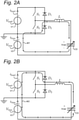
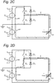
- Figure 2A - 2D show schematically charging and discharging states of the circuitry of Figure 1 .
- a current path W1 for charging in passive mode is shown by a dashed line, where current flows through the second diode D2, while switches S1 and S2 are both open, i.e., non-conductive.
- a current path W2 for discharging in passive mode is depicted. Here the current flows through the first diode D1, while both first and second switches S1, S2 are open.
- a current path W3 for active charging is shown.
- the variable capacitor Cs is charged by the combination of first switch S1 in modulated conductive state and second (free-wheeling) diode D2 along current path W1 and W3.
- the first voltage source V1 is additionally coupled to the variable capacitor Cs for providing charge.
- Discharging in the active mode takes place along a current path W4 as shown in Figure 2D , where the second switch S2 is in modulated conductive state and the first switch S1 is in non-conductive state, which results in a current path W2 and W4 through both the first (free-wheeling) diode D1 and the second switch S2.
- charging is thus performed by a step-down converter similar circuitry and discharging by a step-up converter similar circuitry.
- the control of the active mode of the proposed topology may consist of a low-level modulator implementing e.g. Pulse Width Modulation (PWM) along with closed-loop control on the output voltage.
- PWM Pulse Width Modulation
- synchronous rectification is applied in the active mode for intervals in which the (freewheeling) diode is conducting, and/or in the passive mode when the diode is clamping the variable capacitor to either V low or V high .
- the controller is coupled to a clock signal generator CG and comprises modulating circuitry M in which modulators that are arranged in the controller CT are each coupled to an associated one of the switches S1, S2 of all variable capacitors to share a common switching clock signal for synchronous operation.
- Each modulator would be assigned a relative phase, statically or dynamically, by which the step-up and step-down converters of all variable capacitors are interleaving their currents.
- a grounding connection GND is applied at the interconnecting node N1 between the two voltage sources VI, V2.
- the resulting topology has both voltage sources V1, V2 referenced to ground potential, as well as the half-bridges connected to ground potential. It is observed that advantageously, such a connection scheme reduces the complexity of the voltage source and half-bridge components and their support circuits.
- the grounding connection GND is arranged at the level of the second terminal T21 of the second voltage source V2.
- the invention provides that the variable capacitor Cs and/or connecting cables thereof has/have an outer shield (not shown) that is connected to ground potential GND. Accordingly, the energy harvesting system has favorable characteristics in terms of insulation voltage rating, safety and electromagnetic interference (EMI).
- EMI electromagnetic interference
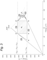
- Figure 3 shows a charge-voltage q,V diagram of a variable capacitor Cs relating to the charging and discharging states shown in Figure 2A - 2D .
- FIG 3 an exemplary charge - voltage q,V diagram is shown for a variable capacitor Cs. It will be appreciated that the value ranges that are shown are only indicative. The invention is not limited to a circuitry and/or a method operating within the ranges shown in Figure 3 , but may operate in different ranges of voltage and charge and with either positive or negative polarity for both voltage and charge.
- Operating variable capacitors Cs in generator mode involves the application of charge (charging) at a state of maximum capacitance and subsequent removal of charge (discharging) at a state of minimum capacitance.
- the challenge of electrostatic energy conversion is the cyclic displacement of charge, the amount of energy involved therein is often several times higher than the amount of mechanical energy to be converted.
- the displacement of charge within the energy harvesting system 100 is fully controllable.
- the charge displacement is driven only indirectly by the imposed capacitance variation and its rate of change.
- the method co-operates the passive (diodes D1, D2) and active (switches S1, S2) elements in the topology of the energy harvesting system 100 during the harvesting cycle: charge is displaced passively as much as possible using deformation-induced (passive) voltage-clamping to the voltages V low , V high as if it was a passive harvesting cycle, while additional charges are displaced actively by charging/discharging as in active harvesting cycle portions such as constant-charge, constant-voltage and constant-field.
- the active harvesting cycle portion involves a constant-field cycle i.e., the electric field is kept constant under a variation of the gap between the electrodes of the variable capacitor.
- the resulting hybrid harvesting cycle then constitutes a combined constant-voltage (indicated in figure 3 as stages P1 and P4) and constant-field (indicated as stage P3) cycle. It is identified that such cycle yields maximum energy within the limits of the voltage rating of the deployed active components (switches S1, S2 and diodes D1, D2).
- the first switch S1 (step-down switch) is set to the modulated conductive state.
- the first switch S1 and second diode D2 actively allow the charging process along current paths W3 and W1 to continue to charge q 3 larger than q 2 . For example, this interval lasts between 1% to 15% of the cycle period, where the former captures more energy from the variable capacitor, and the latter generates lower losses.
- variable capacitor Cs is charged to maximal charge q 4 which approaches or is located at the maximum electric field boundary.
- maximum electric field boundary relation between charge q and voltage V is indicated by the dotted curve referenced as "field limit”.
- stage P3 the charging and discharging cycle follows a q,V path during which the variable capacitor is gradually and actively discharged from q 3 (or q 4 ) to q 2' using the second switch S2 in the modulated conductive state and the first diode D1.
- the first switch S1 is set to the non-conductive state during P3.
- Charge q 2' may be equal to charge q 2 .
- the q.V path follows a constant field q,V relationship.
- variable capacitor voltage v cap has increased to voltage V high (at q 2' )
- variable capacitor Cs is passively discharged from charge q 2' to charge q 1' along current path W2 using the first diode (clamping diode) D1 while both first and second switches S1, S2 are set in non-conductive state.
- the duration of the latter interval is typically in the same order of duration as in stage P2, such that the charging and discharging current are of largely similar magnitude.
- the active discharging terminates when the voltage of the variable capacitor has substantially reached V low at q 0 .
- the invention relates to a method for operating an energy harvesting system 100 for harvesting electrical energy from at least one variable capacitor Cs, as described above, in which the variable capacitor that may comprise electrode layers separated by a deformable dielectric layer, is exposed to a cycle of mechanical loading and unloading, with a capacitance of the variable capacitor varying between a maximum capacitance at a minimal thickness of the dielectric layer during mechanical loading and a minimum capacitance during mechanical unloading.
- the method comprises:
- the method comprises:
- the method further comprises during the charging time interval:
- the method further comprises during the discharging time interval: after reaching q 3 (or q 4 ), setting the first switch in the non-conductive state and setting or holding the second switch in the modulated conductive state, for allowing discharging of the at least one variable capacitor until the voltage of the at least one variable capacitor reaches the value of the voltage V high ; subsequently, when the voltage of the at least one variable capacitor has reached the value of the voltage V high , setting the second switch in the non-conductive state and setting or holding the first switch in the non-conductive state, for allowing further discharging of the at least one variable capacitor until the minimum capacitance is reached at charge q 1 ' and voltage V high .
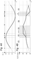
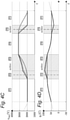
- Figure 4A - 4E show a deformation, an electric field, a voltage, a charge and a current respectively of a variable capacitor coupled to the circuitry of Figure 1 .
- FIG 4A a deformation cycle indicated by stretch parameter ⁇ (stretching and relaxing) of an electro-active polymer based variable capacitor is shown as a function of time.
- stretch parameter ⁇ stretch parameter
- Figure 4B the variation of the electric field E c is shown in Figure 4B
- Figure 4C the variation of the voltage v cap on the variable capacitor is shown in Figure 4C
- Figure 4D the variation of the charge q c on the variable capacitor is shown in Figure 4D
- the variation of the variable capacitor's current i cap is shown in Figure 4E , respectively.
- the stages P1, P2, P3, P4 and P5 as described above with reference to Figure 3 are indicated in each of Figures 4A - 4E .
- the elastic stretch parameter ⁇ is defined as the ratio of the strained length and the relaxed (i.e., not strained) length of the electro-active polymer based variable capacitor.
- each of Figure 4B - 4C the variations originated in accordance with the energy harvesting system and method of the invention are represented by a solid line for the condition that charging of the variable capacitor takes place until the maximum electric field boundary is reached at q 4 .
- the dashed line in each of Figures 4B - 4E represent the variations in a harvesting cycle according to a method of the invention, where charging is done actively to a charge q 3 , in which
- Discharging is done from charge q 1' to charge q 0 , with
- the dotted line in each of Figures 4B - 4E represent the variations in a passive-only harvesting cycle using only passive clamping diodes D1, D2.
- the stages P2, P3 and P5 in which either first switch S1 or second switch S2 are activated to the modulated conductive state are indicated by the hatched areas; the remaining intervals of the cycle are realized while both first and second switches S1, S2 are in the non-conductive state.
- Figure 5 shows a flow diagram 500 for a method of operation of the energy harvesting system according to an embodiment of the invention.
- the controller CT is arranged to control an energy harvesting cycle of the energy harvesting system in accordance with steps in a procedure 500 as shown in the flow diagram.
- the controller comprises at least a processor which is coupled to a memory.
- the memory is arranged to store instructions for the processor to carry out a control program in accordance with the procedure.
- the controller could be implemented as a state machine.
- the energy harvesting cycle starts at an arbitrary capacitance C(t) e.g., equal to or near minimum capacitance C min , while the capacitance is increasing (dC/dt > 0), i.e., while the gap G between the electrodes E1, E2 of the variable capacitor Cs is decreasing e.g., due to an external mechanical force.
- the energy harvesting system 100 is in stage P1 and the variable capacitor Cs clamped to V low with both the first and second switches S1, S2 in non-conductive state in step 504. In this manner, the variable capacitor is charged by current flowing through the second diode D2.
- step 506 the controller CT monitors by means of the current sensor Sc if the current i cap through the variable capacitor becomes essentially zero (i.e., and taking into account possible systematic current leakage). If the current i cap is not zero, the energy harvesting system remains in stage P1 with the variable capacitor clamped to V low . However if the current i cap becomes zero, in step 508 the controller CT activates the first switch S1 to modulated conductive state to allow the variable capacitor to charge to maximal electrical field E high at q 4 or an intermediate electrical field E q3 at q 3 . During charging to q 4 or to q 3 , the energy harvesting system is in stage P2.
- step 510 the controller CT returns the first switch S1 to the open non-conductive state.
- stage P3 the controller CT activates the second switch S2 to allow the variable capacitor to discharge in order to keep the electric field constant.
- step 510 If the voltage v cap on the variable capacitor is smaller than V high then the procedure returns to step 510. If the controller detects by sensor Sv that the voltage v cap on the variable capacitor is equal to V high , then the procedure continues in step 514.
- step 514 the controller CT returns the second switch S2 to the non-conductive state which causes the variable capacitor to discharge over the first diode D1, while both first and second switches S1, S2 are in non-conductive state.
- step 514 the energy harvesting system is in stage P4.
- step 516 the controller CT monitors by means of the current sensor Sc if the current i cap through the variable capacitor Cs becomes essentially zero to detect an end of the discharging step 514. If the current i cap through the variable capacitor Cs becomes zero, in step 518 the detector activates the second switch S2 to the modulated conductive state to discharge further until the voltage on the variable capacitor reaches V low . In step 518, the energy harvesting system is in stage P5.
- step 520 the controller checks if the voltage v cap over the variable capacitor has reached V low by means of the voltage sensor Sv. If the voltage v cap over the variable capacitor has reached V low , then the procedure returns to step 504 (stage PI), otherwise step 518 is continued.
Landscapes
- Physics & Mathematics (AREA)
- General Physics & Mathematics (AREA)
- Charge And Discharge Circuits For Batteries Or The Like (AREA)
- Dc-Dc Converters (AREA)
- Rectifiers (AREA)
Claims (15)
- Energiegewinnungssystem (100) zum Gewinnen von elektrischer Energie aus mindestens einem variablen Kondensator (Cs), umfassend den mindestens einen variablen Kondensator, eine erste Spannungsquelle (V1) zum Bereitstellen einer ersten Spannung (Vload) und eine zweite Spannungsquelle (V2) zum Bereitstellen einer zweiten Spannung (Vbias), für jeden variablen Kondensator ein jeweiliges Halbbrückennetzwerk (H1);wobei die erste und die zweite Spannungsquelle (V1, V2) in einer Reihenschaltung mit einem Verbindungsknoten (N1) zwischen einem Anschluss (T11) erster Polarität der ersten Spannungsquelle und einem Anschluss (T22) zweiter Polarität der zweiten Spannungsquelle angeordnet sind, wobei die zweite Polarität entgegengesetzt zur ersten Polarität ist;wobei das jeweilige Halbbrückennetzwerk ein Paar einer ersten Diode (D1) und einer zweiten Diode (D2) umfasst, die in Reihe mit einem gemeinsamen Knoten (N2) zwischen der ersten und der zweiten Diode geschaltet sind, wobei das Paar parallel zur ersten Spannungsquelle zwischen dem Anschluss (T11) erster Polarität und einem Anschluss (T12) zweiter Polarität der ersten Spannungsquelle geschaltet ist; wobei der mindestens eine variable Kondensator mit einem ersten Kondensatoranschluss (TC1) zum gemeinsamen Knoten (N2) und mit einem zweiten Kondensatoranschluss (TC2) zu einem Anschluss (T21) erster Polarität der zweiten Spannungsquelle (V2) verbunden ist;
wobeifür jeden variablen Kondensator das System ferner einen Induktor (L1), einen ersten Schalter (S1) und einen zweiten Schalter (S2) umfasst;der Induktor (L1) zwischen dem gemeinsamen Knoten (N2) und dem ersten Kondensatoranschluss (TC1) des jeweiligen variablen Kondensators geschaltet ist, undder erste Schalter (S1) parallel zur ersten Diode (D1) geschaltet ist und der zweite Schalter (S2) parallel zur zweiten Diode (D2) geschaltet ist. - Energiegewinnungssystem nach Anspruch 1, wobei der mindestens eine variable Kondensator eine elektroaktive Polymervorrichtung ist, die eine erste Elektrodenschicht, eine zweite Elektrodenschicht und eine dielektrische Elastomerschicht umfasst, wobei die dielektrische Elastomerschicht zwischen der ersten und der zweiten Elektrodenschicht angeordnet ist.
- Energiegewinnungssystem nach einem der vorhergehenden Ansprüche, ferner umfassend eine Steuerung (CT); wobei die Steuerung mit dem ersten und dem zweiten Schalter (S1, S2) im Halbbrückennetzwerk (H1) verbunden ist, um einen Schaltzustand für jeden der Schalter zu steuern.
- Energiegewinnungssystem nach einem der Ansprüche 1-3, wobei jeder des ersten und des zweiten Schalters ein Treiberelement zum aktiven Ein- und Ausschalten des jeweiligen Schalters mit einer vorbestimmten Schaltrate umfasst; wobei die Schaltrate optional basierend auf einer gemessenen Spannung am variablen Kondensator und/oder auf einem gemessenen Lade- oder Entladestrom dynamisch eingestellt wird.
- Energiegewinnungssystem nach Anspruch 3 oder 4, wobei die Steuerung (CT) für jeden variablen Kondensator eine Modulatorvorrichtung (M) zum Bereitstellen eines Modulationssignals an einen oder mehrere der Schalter umfasst.
- Energiegewinnungssystem nach einem der Ansprüche 3-5, wobei die Steuerung einen Spannungssensor (Sv) zum Messen einer Spannung vcap über dem mindestens einen variablen Kondensator und einen Stromsensor (Sc) zum Messen eines Stroms icap durch den variablen Kondensator umfasst.
- Energiegewinnungssystem nach einem der Ansprüche 3-6, wobei die Steuerung konfiguriert ist, um eine Ausgangsspannung mittels einer Schleifensteuerung basierend auf einer am variablen Kondensator gemessenen Spannung zu regeln.
- Energiegewinnungssystem nach einem der vorhergehenden Ansprüche 5-7, ferner umfassend mindestens einen zweiten variablen Kondensator (CS2), wobei der mindestens zweite variable Kondensator mit einem ersten Kondensatoranschluss (TC1-2) davon mit dem gemeinsamen Knoten (N22) und mit einem zweiten Kondensatoranschluss (TC2-2) davon mit dem Anschluss (T21) erster Polarität der zweiten Spannungsquelle (V2) verbunden ist, und für jeden variablen Kondensator die Steuerung mit einem Taktsignalgenerator (CG) zum Bereitstellen einer jeweiligen Modulatorvorrichtung (M) konfiguriert ist, die zum Modulieren mindestens eines der ersten und zweiten Schalter mit einem gemeinsamen Taktsignal für den synchronen Betrieb des Energiegewinnungssystems für den mindestens einen und den zweiten variablen Kondensator angeordnet ist; wobei die Modulatorvorrichtung jedes der mindestens ersten und zweiten variablen Kondensatoren konfiguriert ist, um eine jeweilige Phase relativ zum gemeinsamen Taktsignal aufzuweisen.
- Energiegewinnungssystem nach einem der vorhergehenden Ansprüche, wobei entweder ein Masseanschluss (GND) am Verbindungsknoten (N1) zwischen der ersten und der zweiten Spannungsquelle oder ein Masseanschluss (GND) am zweiten Anschluss (T21) der zweiten Spannungsquelle (V2) vorgesehen ist.
- Energiegewinnungssystem nach einem der vorhergehenden Ansprüche, wobei die erste Spannungsquelle mindestens einen Widerstand umfasst, und wobei die erste Spannungsquelle konfiguriert ist, um eine erste Spannung als Funktion der Ladungsverschiebung zu erzeugen, die durch den mindestens einen variablen Kondensator durch das zugehörige Halbbrückennetzwerk auferlegt wird.
- Verfahren zum Betreiben eines Energiegewinnungssystems (100) zum Gewinnen von elektrischer Energie aus mindestens einem variablen Kondensator (Cs; Cs2) mit einer Kapazität, die als Funktion der mechanischen Verformung variabel ist, nach Anspruch 1,wobei der mindestens eine variable Kondensator einem Zyklus (λ) mechanischer Belastung und Entlastung ausgesetzt ist, wobei die Kapazität des variablen Kondensators zwischen einer maximalen Kapazität während maximaler mechanischer Belastung und einer minimalen Kapazität während minimaler mechanischer Belastung variiert,wobei das Verfahren umfasst:- elektrisches Entladen des mindestens einen variablen Kondensators während des mechanischen Entladens in einem Entladezeitintervall (P4) über die erste Diode, während sich der erste und der zweite Schalter im nicht leitenden Zustand befinden,- elektrisches Laden des mindestens einen variablen Kondensators während des mechanischen Ladens in einem Ladezeitintervall (P1) über die zweite Diode, während sich der erste und der zweite Schalter im nicht leitenden Zustand befinden, undwobei das Verfahren umfasst:Einstellen des zweiten Schalters in einen modulierten leitenden Zustand während eines Abschnitts des Entladezeitintervalls (P3; P5), während der erste Schalter im nicht leitenden Zustand bleibt oder auf diesen eingestellt ist, undEinstellen des ersten Schalters in einen modulierten leitenden Zustand während eines Abschnitts des Ladezeitintervalls (P2), während der zweite Schalter im nicht leitenden Zustand bleibt oder auf diesen eingestellt ist.
- Verfahren nach Anspruch 11, umfassend während des Ladezeitintervalls:- Klemmen (P1) der zweiten Spannungsquelle (V2) bei der zweiten Spannung (Vbias) an den mindestens einen variablen Kondensator mit dem ersten und dem zweiten Schalter (S1, S2) in einem nicht leitenden Zustand, bis die maximale Kapazität und eine erste Ladung q2 erreicht sind, und anschließend- Klemmen (P2) der ersten Spannungsquelle (V1) bei der ersten Spannung (Vload) an den mindestens einen variablen Kondensator in Reihe mit der zweiten Spannungsquelle (V2) bei der zweiten Spannung (Vbias) durch Einstellen des ersten Schalters (S1) in den modulierten leitenden Zustand, bis eine zweite Ladung q3 des mindestens einen variablen Kondensators mit q3>q2 erreicht ist oder sich eine dritte Ladung q4 einem maximalen elektrischen Feldgrenzwert mit q4>q3>q2 erreicht oder sich diesem nähert.
- Verfahren nach Anspruch 11 oder 12, umfassend während des Entladezeitintervalls:nach Erreichen des zweiten Ladungswerts q3 oder des dritten Ladungswerts q4: Einstellen des ersten Schalters in den nichtleitenden Zustand und Halten des zweiten Schalters im modulierten leitenden Zustand, um das Entladen des mindestens einen variablen Kondensators zu ermöglichen, bis die Spannung des mindestens einen variablen Kondensators den Wert der Summe der ersten Spannung und der zweiten Spannung Vbias+Vload (P3) erreicht;anschließend, wenn die Spannung des mindestens einen variablen Kondensators den Wert von Vbias+Vload erreicht hat: Einstellen des zweiten Schalters in den nichtleitenden Zustand und Belassen des ersten Schalters im nichtleitenden Zustand, um das weitere Entladen des mindestens einen variablen Kondensators zu ermöglichen, bis eine vierte Ladung q1 beim Wert Vbias+Vload erreicht wird (P4),
undanschließend Einstellen des zweiten Schalters im modulierten leitenden Zustand, um das zusätzliche Entladen des mindestens einen variablen Kondensators von der vierten Ladung q1 auf eine fünfte Ladung q0 beim Wert der zweiten Spannung (Vbias) zu ermöglichen, wobei der fünfte Ladungswert q0 kleiner als jeder von q1, q2, q3, q4 ist. - Verfahren nach einem der vorhergehenden Ansprüche 11-13, wobei zum Steuern des Zyklus des Energiegewinnungssystems das Verfahren umfasst:Ableiten oder Messen einer Intensität eines elektrischen Felds über dem variablen Kondensator, unter der Annahme, dass ein Zustand maximaler und minimaler Kapazität unter Verwendung einer Nullstromerfassung beobachtet wird, mit einem Strom durch den Kondensator icap == 0,ferner umfassend das Messen der Kondensatorspannung vcap und entweder das Messen eines Abstands des Spalts zwischen Elektroden des Kondensators oder das Ableiten des Abstands des Spalts von einer Kapazität, die aus der gemessenen Kondensatorspannung vcap und dem gemessenen Kondensatorstrom icap bestimmt wird.
- Verfahren nach Anspruch 14, wobei die maximale Kapazität oder minimale Kapazität
durch Messen eines Nulldurchgangs des Stroms durch den Kondensator bestimmt wird.
Applications Claiming Priority (2)
| Application Number | Priority Date | Filing Date | Title |
|---|---|---|---|
| EP17208623 | 2017-12-19 | ||
| PCT/EP2018/085750 WO2019121860A1 (en) | 2017-12-19 | 2018-12-19 | Switch assisted diode-clamped energy harvesting system for variable capacitance transducers |
Publications (2)
| Publication Number | Publication Date |
|---|---|
| EP3729633A1 EP3729633A1 (de) | 2020-10-28 |
| EP3729633B1 true EP3729633B1 (de) | 2022-01-26 |
Family
ID=60937548
Family Applications (1)
| Application Number | Title | Priority Date | Filing Date |
|---|---|---|---|
| EP18826001.2A Active EP3729633B1 (de) | 2017-12-19 | 2018-12-19 | Schalterunterstütztes diodengeklemmtes energiesammelsystem für wandler mit variabler kapazität |
Country Status (6)
| Country | Link |
|---|---|
| US (1) | US11218087B2 (de) |
| EP (1) | EP3729633B1 (de) |
| JP (1) | JP7280267B2 (de) |
| CN (1) | CN111492570B (de) |
| DK (1) | DK3729633T3 (de) |
| WO (1) | WO2019121860A1 (de) |
Families Citing this family (2)
| Publication number | Priority date | Publication date | Assignee | Title |
|---|---|---|---|---|
| FR3076409A1 (fr) | 2017-12-28 | 2019-07-05 | Commissariat A L'energie Atomique Et Aux Energies Alternatives | Circuit et procede de recuperation d'energie |
| US11316446B2 (en) * | 2020-06-02 | 2022-04-26 | Honeywell Federal Manufacturings Technologies, Llc | Electrostatic energy harvester |
Family Cites Families (14)
| Publication number | Priority date | Publication date | Assignee | Title |
|---|---|---|---|---|
| US6580177B1 (en) | 1999-06-01 | 2003-06-17 | Continuum Control Corporation | Electrical power extraction from mechanical disturbances |
| CA2376063A1 (en) | 1999-06-01 | 2000-12-07 | Continuum Control Corporation | Electrical power extraction from mechanical disturbances |
| US7977923B2 (en) * | 2007-03-09 | 2011-07-12 | Sri International | Circuits for electroactive polymer generators |
| US9279409B2 (en) * | 2009-06-16 | 2016-03-08 | Single Buoy Moorings, Inc. | Environmental electrical generator |
| JP5589729B2 (ja) | 2010-09-30 | 2014-09-17 | 大日本印刷株式会社 | 圧電素子発電回路 |
| DK2847856T3 (en) * | 2012-05-10 | 2018-08-06 | Single Buoy Moorings | Charging / Discharging Circuits for Electromechanical Energy Conversion and Electromechanical Energy Conversion System |
| US9231473B2 (en) * | 2012-05-10 | 2016-01-05 | Single Buoy Moorings Inc. | Increasing EAP conversion efficiency by continuous current |
| DE102012208557A1 (de) | 2012-05-22 | 2013-11-28 | Robert Bosch Gmbh | Generatoren aus elektroaktiven Polymeren (EAP) in Differenzanordnung |
| JP6541271B2 (ja) * | 2013-11-13 | 2019-07-10 | シングル ブイ ムーリングス インコーポレイテッド | 多相eapシステムおよびそのシステムを制御する方法 |
| US10116208B2 (en) * | 2014-01-28 | 2018-10-30 | Stmicroelectronics S.R.L. | DC-DC converter with improved energy management, method for operating the DC-DC converter, environmental energy harvesting system using the DC-DC converter, and apparatus using the energy harvesting system |
| JP2016127656A (ja) | 2014-12-26 | 2016-07-11 | ムネカタ株式会社 | 環境発電素子で発生した電力を蓄電する蓄電装置 |
| CN106602687A (zh) * | 2015-10-19 | 2017-04-26 | 北京纳米能源与系统研究所 | 摩擦纳米发电机的能量管理方法、电路和装置 |
| RU2718672C2 (ru) * | 2015-12-03 | 2020-04-13 | Конинклейке Филипс Н.В. | Система и способ генерации энергии |
| US11096429B2 (en) * | 2017-06-13 | 2021-08-24 | Analog Devices, Inc. | System and method for wireless charging of smart garments |
-
2018
- 2018-12-19 DK DK18826001.2T patent/DK3729633T3/da active
- 2018-12-19 WO PCT/EP2018/085750 patent/WO2019121860A1/en not_active Ceased
- 2018-12-19 EP EP18826001.2A patent/EP3729633B1/de active Active
- 2018-12-19 JP JP2020534496A patent/JP7280267B2/ja active Active
- 2018-12-19 CN CN201880082730.7A patent/CN111492570B/zh active Active
- 2018-12-19 US US16/956,416 patent/US11218087B2/en active Active
Also Published As
| Publication number | Publication date |
|---|---|
| US20210104960A1 (en) | 2021-04-08 |
| US11218087B2 (en) | 2022-01-04 |
| DK3729633T3 (da) | 2022-02-21 |
| JP7280267B2 (ja) | 2023-05-23 |
| EP3729633A1 (de) | 2020-10-28 |
| WO2019121860A1 (en) | 2019-06-27 |
| CN111492570A (zh) | 2020-08-04 |
| JP2021507668A (ja) | 2021-02-22 |
| CN111492570B (zh) | 2023-10-27 |
Similar Documents
| Publication | Publication Date | Title |
|---|---|---|
| CN103748758B (zh) | 升压变换器 | |
| EP1852963B1 (de) | Stromrichteranordnung | |
| JP5729732B2 (ja) | 直流電源装置、直流電源装置の制御方法 | |
| JP6174125B2 (ja) | 電気機械エネルギー変換のための充電/放電回路および電気機械エネルギー変換システム | |
| WO2013135118A1 (en) | Apparatus and method for feedforward controlled charge pumps | |
| US10027234B2 (en) | Power conversion device for performing power conversion between DC and DC by controlling switching of a semiconductor switching element | |
| EP3729633B1 (de) | Schalterunterstütztes diodengeklemmtes energiesammelsystem für wandler mit variabler kapazität | |
| JP5761620B2 (ja) | 接地可能dc/dcコンバータ | |
| ITVA20100043A1 (it) | Diodo di by-pass o interruttore per sorgente dc realizzato con un mosfet a bassa resistenza di conduzione e relativo circuito di controllo autoalimentato con mezzi di disabilitazione della sorgente dc in caso di incendio o altro rischio | |
| JP6928013B2 (ja) | 電源装置 | |
| KR102077026B1 (ko) | 태양 에너지 충전장치 및 그 제어방법 | |
| WO2021028990A1 (ja) | Dc-dcコンバータ | |
| JP4253809B2 (ja) | Dc−dcコンバータ | |
| KR102077027B1 (ko) | 태양 에너지 충전장치 및 그 제어방법 | |
| KR102077028B1 (ko) | 태양 에너지 충전장치 및 그 제어방법 | |
| KR102077021B1 (ko) | 태양 에너지 충전장치 및 그 제어방법 | |
| KR102077024B1 (ko) | 태양 에너지 충전장치 및 그 제어방법 | |
| KR102077022B1 (ko) | 태양 에너지 충전장치 및 그 제어방법 | |
| KR102077023B1 (ko) | 태양 에너지 충전장치 및 그 제어방법 | |
| KR102077025B1 (ko) | 태양 에너지 충전장치 및 그 제어방법 | |
| Wang et al. | Practical considerations of the start-up procedure for an active capacitor | |
| KR100679984B1 (ko) | 전류원 rf 전원회로 | |
| JP5523499B2 (ja) | 電力変換装置 | |
| JPWO2023095265A5 (de) | ||
| KR19990066292A (ko) | 대전력 펄스 발생장치 |
Legal Events
| Date | Code | Title | Description |
|---|---|---|---|
| STAA | Information on the status of an ep patent application or granted ep patent |
Free format text: STATUS: UNKNOWN |
|
| STAA | Information on the status of an ep patent application or granted ep patent |
Free format text: STATUS: THE INTERNATIONAL PUBLICATION HAS BEEN MADE |
|
| PUAI | Public reference made under article 153(3) epc to a published international application that has entered the european phase |
Free format text: ORIGINAL CODE: 0009012 |
|
| STAA | Information on the status of an ep patent application or granted ep patent |
Free format text: STATUS: REQUEST FOR EXAMINATION WAS MADE |
|
| 17P | Request for examination filed |
Effective date: 20200706 |
|
| AK | Designated contracting states |
Kind code of ref document: A1 Designated state(s): AL AT BE BG CH CY CZ DE DK EE ES FI FR GB GR HR HU IE IS IT LI LT LU LV MC MK MT NL NO PL PT RO RS SE SI SK SM TR |
|
| AX | Request for extension of the european patent |
Extension state: BA ME |
|
| DAV | Request for validation of the european patent (deleted) | ||
| DAX | Request for extension of the european patent (deleted) | ||
| GRAP | Despatch of communication of intention to grant a patent |
Free format text: ORIGINAL CODE: EPIDOSNIGR1 |
|
| STAA | Information on the status of an ep patent application or granted ep patent |
Free format text: STATUS: GRANT OF PATENT IS INTENDED |
|
| INTG | Intention to grant announced |
Effective date: 20210810 |
|
| GRAS | Grant fee paid |
Free format text: ORIGINAL CODE: EPIDOSNIGR3 |
|
| GRAA | (expected) grant |
Free format text: ORIGINAL CODE: 0009210 |
|
| STAA | Information on the status of an ep patent application or granted ep patent |
Free format text: STATUS: THE PATENT HAS BEEN GRANTED |
|
| AK | Designated contracting states |
Kind code of ref document: B1 Designated state(s): AL AT BE BG CH CY CZ DE DK EE ES FI FR GB GR HR HU IE IS IT LI LT LU LV MC MK MT NL NO PL PT RO RS SE SI SK SM TR |
|
| REG | Reference to a national code |
Ref country code: GB Ref legal event code: FG4D |
|
| REG | Reference to a national code |
Ref country code: CH Ref legal event code: EP |
|
| REG | Reference to a national code |
Ref country code: AT Ref legal event code: REF Ref document number: 1466058 Country of ref document: AT Kind code of ref document: T Effective date: 20220215 |
|
| REG | Reference to a national code |
Ref country code: IE Ref legal event code: FG4D |
|
| REG | Reference to a national code |
Ref country code: DE Ref legal event code: R096 Ref document number: 602018030211 Country of ref document: DE |
|
| REG | Reference to a national code |
Ref country code: DK Ref legal event code: T3 Effective date: 20220215 |
|
| REG | Reference to a national code |
Ref country code: NL Ref legal event code: FP |
|
| REG | Reference to a national code |
Ref country code: LT Ref legal event code: MG9D |
|
| REG | Reference to a national code |
Ref country code: AT Ref legal event code: MK05 Ref document number: 1466058 Country of ref document: AT Kind code of ref document: T Effective date: 20220126 |
|
| PG25 | Lapsed in a contracting state [announced via postgrant information from national office to epo] |
Ref country code: SE Free format text: LAPSE BECAUSE OF FAILURE TO SUBMIT A TRANSLATION OF THE DESCRIPTION OR TO PAY THE FEE WITHIN THE PRESCRIBED TIME-LIMIT Effective date: 20220126 Ref country code: RS Free format text: LAPSE BECAUSE OF FAILURE TO SUBMIT A TRANSLATION OF THE DESCRIPTION OR TO PAY THE FEE WITHIN THE PRESCRIBED TIME-LIMIT Effective date: 20220126 Ref country code: PT Free format text: LAPSE BECAUSE OF FAILURE TO SUBMIT A TRANSLATION OF THE DESCRIPTION OR TO PAY THE FEE WITHIN THE PRESCRIBED TIME-LIMIT Effective date: 20220526 Ref country code: NO Free format text: LAPSE BECAUSE OF FAILURE TO SUBMIT A TRANSLATION OF THE DESCRIPTION OR TO PAY THE FEE WITHIN THE PRESCRIBED TIME-LIMIT Effective date: 20220426 Ref country code: LT Free format text: LAPSE BECAUSE OF FAILURE TO SUBMIT A TRANSLATION OF THE DESCRIPTION OR TO PAY THE FEE WITHIN THE PRESCRIBED TIME-LIMIT Effective date: 20220126 Ref country code: HR Free format text: LAPSE BECAUSE OF FAILURE TO SUBMIT A TRANSLATION OF THE DESCRIPTION OR TO PAY THE FEE WITHIN THE PRESCRIBED TIME-LIMIT Effective date: 20220126 Ref country code: ES Free format text: LAPSE BECAUSE OF FAILURE TO SUBMIT A TRANSLATION OF THE DESCRIPTION OR TO PAY THE FEE WITHIN THE PRESCRIBED TIME-LIMIT Effective date: 20220126 Ref country code: BG Free format text: LAPSE BECAUSE OF FAILURE TO SUBMIT A TRANSLATION OF THE DESCRIPTION OR TO PAY THE FEE WITHIN THE PRESCRIBED TIME-LIMIT Effective date: 20220426 |
|
| PG25 | Lapsed in a contracting state [announced via postgrant information from national office to epo] |
Ref country code: PL Free format text: LAPSE BECAUSE OF FAILURE TO SUBMIT A TRANSLATION OF THE DESCRIPTION OR TO PAY THE FEE WITHIN THE PRESCRIBED TIME-LIMIT Effective date: 20220126 Ref country code: LV Free format text: LAPSE BECAUSE OF FAILURE TO SUBMIT A TRANSLATION OF THE DESCRIPTION OR TO PAY THE FEE WITHIN THE PRESCRIBED TIME-LIMIT Effective date: 20220126 Ref country code: GR Free format text: LAPSE BECAUSE OF FAILURE TO SUBMIT A TRANSLATION OF THE DESCRIPTION OR TO PAY THE FEE WITHIN THE PRESCRIBED TIME-LIMIT Effective date: 20220427 Ref country code: FI Free format text: LAPSE BECAUSE OF FAILURE TO SUBMIT A TRANSLATION OF THE DESCRIPTION OR TO PAY THE FEE WITHIN THE PRESCRIBED TIME-LIMIT Effective date: 20220126 Ref country code: AT Free format text: LAPSE BECAUSE OF FAILURE TO SUBMIT A TRANSLATION OF THE DESCRIPTION OR TO PAY THE FEE WITHIN THE PRESCRIBED TIME-LIMIT Effective date: 20220126 |
|
| PG25 | Lapsed in a contracting state [announced via postgrant information from national office to epo] |
Ref country code: IS Free format text: LAPSE BECAUSE OF FAILURE TO SUBMIT A TRANSLATION OF THE DESCRIPTION OR TO PAY THE FEE WITHIN THE PRESCRIBED TIME-LIMIT Effective date: 20220526 |
|
| REG | Reference to a national code |
Ref country code: DE Ref legal event code: R097 Ref document number: 602018030211 Country of ref document: DE |
|
| PG25 | Lapsed in a contracting state [announced via postgrant information from national office to epo] |
Ref country code: SM Free format text: LAPSE BECAUSE OF FAILURE TO SUBMIT A TRANSLATION OF THE DESCRIPTION OR TO PAY THE FEE WITHIN THE PRESCRIBED TIME-LIMIT Effective date: 20220126 Ref country code: SK Free format text: LAPSE BECAUSE OF FAILURE TO SUBMIT A TRANSLATION OF THE DESCRIPTION OR TO PAY THE FEE WITHIN THE PRESCRIBED TIME-LIMIT Effective date: 20220126 Ref country code: RO Free format text: LAPSE BECAUSE OF FAILURE TO SUBMIT A TRANSLATION OF THE DESCRIPTION OR TO PAY THE FEE WITHIN THE PRESCRIBED TIME-LIMIT Effective date: 20220126 Ref country code: EE Free format text: LAPSE BECAUSE OF FAILURE TO SUBMIT A TRANSLATION OF THE DESCRIPTION OR TO PAY THE FEE WITHIN THE PRESCRIBED TIME-LIMIT Effective date: 20220126 Ref country code: CZ Free format text: LAPSE BECAUSE OF FAILURE TO SUBMIT A TRANSLATION OF THE DESCRIPTION OR TO PAY THE FEE WITHIN THE PRESCRIBED TIME-LIMIT Effective date: 20220126 |
|
| PG25 | Lapsed in a contracting state [announced via postgrant information from national office to epo] |
Ref country code: AL Free format text: LAPSE BECAUSE OF FAILURE TO SUBMIT A TRANSLATION OF THE DESCRIPTION OR TO PAY THE FEE WITHIN THE PRESCRIBED TIME-LIMIT Effective date: 20220126 |
|
| PLBE | No opposition filed within time limit |
Free format text: ORIGINAL CODE: 0009261 |
|
| STAA | Information on the status of an ep patent application or granted ep patent |
Free format text: STATUS: NO OPPOSITION FILED WITHIN TIME LIMIT |
|
| 26N | No opposition filed |
Effective date: 20221027 |
|
| PG25 | Lapsed in a contracting state [announced via postgrant information from national office to epo] |
Ref country code: SI Free format text: LAPSE BECAUSE OF FAILURE TO SUBMIT A TRANSLATION OF THE DESCRIPTION OR TO PAY THE FEE WITHIN THE PRESCRIBED TIME-LIMIT Effective date: 20220126 |
|
| P01 | Opt-out of the competence of the unified patent court (upc) registered |
Effective date: 20230525 |
|
| PG25 | Lapsed in a contracting state [announced via postgrant information from national office to epo] |
Ref country code: IT Free format text: LAPSE BECAUSE OF FAILURE TO SUBMIT A TRANSLATION OF THE DESCRIPTION OR TO PAY THE FEE WITHIN THE PRESCRIBED TIME-LIMIT Effective date: 20220126 |
|
| REG | Reference to a national code |
Ref country code: CH Ref legal event code: PL |
|
| REG | Reference to a national code |
Ref country code: BE Ref legal event code: MM Effective date: 20221231 |
|
| PG25 | Lapsed in a contracting state [announced via postgrant information from national office to epo] |
Ref country code: LU Free format text: LAPSE BECAUSE OF NON-PAYMENT OF DUE FEES Effective date: 20221219 |
|
| PG25 | Lapsed in a contracting state [announced via postgrant information from national office to epo] |
Ref country code: LI Free format text: LAPSE BECAUSE OF NON-PAYMENT OF DUE FEES Effective date: 20221231 Ref country code: CH Free format text: LAPSE BECAUSE OF NON-PAYMENT OF DUE FEES Effective date: 20221231 |
|
| PG25 | Lapsed in a contracting state [announced via postgrant information from national office to epo] |
Ref country code: BE Free format text: LAPSE BECAUSE OF NON-PAYMENT OF DUE FEES Effective date: 20221231 |
|
| PG25 | Lapsed in a contracting state [announced via postgrant information from national office to epo] |
Ref country code: CY Free format text: LAPSE BECAUSE OF FAILURE TO SUBMIT A TRANSLATION OF THE DESCRIPTION OR TO PAY THE FEE WITHIN THE PRESCRIBED TIME-LIMIT Effective date: 20220126 |
|
| PG25 | Lapsed in a contracting state [announced via postgrant information from national office to epo] |
Ref country code: MK Free format text: LAPSE BECAUSE OF FAILURE TO SUBMIT A TRANSLATION OF THE DESCRIPTION OR TO PAY THE FEE WITHIN THE PRESCRIBED TIME-LIMIT Effective date: 20220126 Ref country code: HU Free format text: LAPSE BECAUSE OF FAILURE TO SUBMIT A TRANSLATION OF THE DESCRIPTION OR TO PAY THE FEE WITHIN THE PRESCRIBED TIME-LIMIT; INVALID AB INITIO Effective date: 20181219 |
|
| PG25 | Lapsed in a contracting state [announced via postgrant information from national office to epo] |
Ref country code: MC Free format text: LAPSE BECAUSE OF FAILURE TO SUBMIT A TRANSLATION OF THE DESCRIPTION OR TO PAY THE FEE WITHIN THE PRESCRIBED TIME-LIMIT Effective date: 20220126 |
|
| PG25 | Lapsed in a contracting state [announced via postgrant information from national office to epo] |
Ref country code: TR Free format text: LAPSE BECAUSE OF FAILURE TO SUBMIT A TRANSLATION OF THE DESCRIPTION OR TO PAY THE FEE WITHIN THE PRESCRIBED TIME-LIMIT Effective date: 20220126 Ref country code: MC Free format text: LAPSE BECAUSE OF FAILURE TO SUBMIT A TRANSLATION OF THE DESCRIPTION OR TO PAY THE FEE WITHIN THE PRESCRIBED TIME-LIMIT Effective date: 20220126 |
|
| PG25 | Lapsed in a contracting state [announced via postgrant information from national office to epo] |
Ref country code: MT Free format text: LAPSE BECAUSE OF FAILURE TO SUBMIT A TRANSLATION OF THE DESCRIPTION OR TO PAY THE FEE WITHIN THE PRESCRIBED TIME-LIMIT Effective date: 20220126 |
|
| PGFP | Annual fee paid to national office [announced via postgrant information from national office to epo] |
Ref country code: NL Payment date: 20251119 Year of fee payment: 8 |
|
| PGFP | Annual fee paid to national office [announced via postgrant information from national office to epo] |
Ref country code: DE Payment date: 20251126 Year of fee payment: 8 |
|
| PGFP | Annual fee paid to national office [announced via postgrant information from national office to epo] |
Ref country code: GB Payment date: 20251119 Year of fee payment: 8 |
|
| PGFP | Annual fee paid to national office [announced via postgrant information from national office to epo] |
Ref country code: DK Payment date: 20251119 Year of fee payment: 8 |
|
| PGFP | Annual fee paid to national office [announced via postgrant information from national office to epo] |
Ref country code: FR Payment date: 20251120 Year of fee payment: 8 |
|
| PGFP | Annual fee paid to national office [announced via postgrant information from national office to epo] |
Ref country code: IE Payment date: 20251121 Year of fee payment: 8 |