EP3726937A1 - Driving light emitting diodes and display apparatus - Google Patents
Driving light emitting diodes and display apparatus Download PDFInfo
- Publication number
- EP3726937A1 EP3726937A1 EP19212574.8A EP19212574A EP3726937A1 EP 3726937 A1 EP3726937 A1 EP 3726937A1 EP 19212574 A EP19212574 A EP 19212574A EP 3726937 A1 EP3726937 A1 EP 3726937A1
- Authority
- EP
- European Patent Office
- Prior art keywords
- node
- switching element
- switching
- leds
- charge pump
- Prior art date
- Legal status (The legal status is an assumption and is not a legal conclusion. Google has not performed a legal analysis and makes no representation as to the accuracy of the status listed.)
- Pending
Links
- 238000000034 method Methods 0.000 claims abstract description 27
- 239000003990 capacitor Substances 0.000 claims description 30
- 230000005669 field effect Effects 0.000 claims description 5
- 238000010586 diagram Methods 0.000 description 8
- 230000008569 process Effects 0.000 description 8
- 239000000203 mixture Substances 0.000 description 4
- 230000008901 benefit Effects 0.000 description 3
- 238000007599 discharging Methods 0.000 description 3
- 238000012545 processing Methods 0.000 description 3
- 230000008878 coupling Effects 0.000 description 2
- 238000010168 coupling process Methods 0.000 description 2
- 238000005859 coupling reaction Methods 0.000 description 2
- 238000013461 design Methods 0.000 description 2
- 230000015556 catabolic process Effects 0.000 description 1
- 238000004891 communication Methods 0.000 description 1
- 238000004590 computer program Methods 0.000 description 1
- 238000007796 conventional method Methods 0.000 description 1
- 238000005516 engineering process Methods 0.000 description 1
- 238000005286 illumination Methods 0.000 description 1
- 238000002955 isolation Methods 0.000 description 1
- 239000000463 material Substances 0.000 description 1
- 238000005259 measurement Methods 0.000 description 1
- 238000012986 modification Methods 0.000 description 1
- 230000004048 modification Effects 0.000 description 1
- 230000003287 optical effect Effects 0.000 description 1
- 230000000007 visual effect Effects 0.000 description 1
Images

Classifications
-
- H—ELECTRICITY
- H05—ELECTRIC TECHNIQUES NOT OTHERWISE PROVIDED FOR
- H05B—ELECTRIC HEATING; ELECTRIC LIGHT SOURCES NOT OTHERWISE PROVIDED FOR; CIRCUIT ARRANGEMENTS FOR ELECTRIC LIGHT SOURCES, IN GENERAL
- H05B45/00—Circuit arrangements for operating light-emitting diodes [LED]
- H05B45/30—Driver circuits
- H05B45/37—Converter circuits
-
- H—ELECTRICITY
- H02—GENERATION; CONVERSION OR DISTRIBUTION OF ELECTRIC POWER
- H02M—APPARATUS FOR CONVERSION BETWEEN AC AND AC, BETWEEN AC AND DC, OR BETWEEN DC AND DC, AND FOR USE WITH MAINS OR SIMILAR POWER SUPPLY SYSTEMS; CONVERSION OF DC OR AC INPUT POWER INTO SURGE OUTPUT POWER; CONTROL OR REGULATION THEREOF
- H02M3/00—Conversion of DC power input into DC power output
- H02M3/02—Conversion of DC power input into DC power output without intermediate conversion into AC
- H02M3/04—Conversion of DC power input into DC power output without intermediate conversion into AC by static converters
- H02M3/06—Conversion of DC power input into DC power output without intermediate conversion into AC by static converters using resistors or capacitors, e.g. potential divider
- H02M3/07—Conversion of DC power input into DC power output without intermediate conversion into AC by static converters using resistors or capacitors, e.g. potential divider using capacitors charged and discharged alternately by semiconductor devices with control electrode, e.g. charge pumps
-
- H—ELECTRICITY
- H05—ELECTRIC TECHNIQUES NOT OTHERWISE PROVIDED FOR
- H05B—ELECTRIC HEATING; ELECTRIC LIGHT SOURCES NOT OTHERWISE PROVIDED FOR; CIRCUIT ARRANGEMENTS FOR ELECTRIC LIGHT SOURCES, IN GENERAL
- H05B45/00—Circuit arrangements for operating light-emitting diodes [LED]
- H05B45/10—Controlling the intensity of the light
-
- H—ELECTRICITY
- H05—ELECTRIC TECHNIQUES NOT OTHERWISE PROVIDED FOR
- H05B—ELECTRIC HEATING; ELECTRIC LIGHT SOURCES NOT OTHERWISE PROVIDED FOR; CIRCUIT ARRANGEMENTS FOR ELECTRIC LIGHT SOURCES, IN GENERAL
- H05B45/00—Circuit arrangements for operating light-emitting diodes [LED]
- H05B45/30—Driver circuits
- H05B45/345—Current stabilisation; Maintaining constant current
-
- Y—GENERAL TAGGING OF NEW TECHNOLOGICAL DEVELOPMENTS; GENERAL TAGGING OF CROSS-SECTIONAL TECHNOLOGIES SPANNING OVER SEVERAL SECTIONS OF THE IPC; TECHNICAL SUBJECTS COVERED BY FORMER USPC CROSS-REFERENCE ART COLLECTIONS [XRACs] AND DIGESTS
- Y02—TECHNOLOGIES OR APPLICATIONS FOR MITIGATION OR ADAPTATION AGAINST CLIMATE CHANGE
- Y02B—CLIMATE CHANGE MITIGATION TECHNOLOGIES RELATED TO BUILDINGS, e.g. HOUSING, HOUSE APPLIANCES OR RELATED END-USER APPLICATIONS
- Y02B20/00—Energy efficient lighting technologies, e.g. halogen lamps or gas discharge lamps
- Y02B20/30—Semiconductor lamps, e.g. solid state lamps [SSL] light emitting diodes [LED] or organic LED [OLED]
Definitions
- the present invention generally relates to light emitting diodes (LEDs), and more specifically, to circuit and method for driving LEDs and display apparatus.
- LEDs light emitting diodes
- a light-emitting diode (LED) circuit (also referred to as an LED driver) is an electrical circuit used for an LED.
- the circuit provides sufficient current to light the LED at the required brightness, while also limiting the current to prevent damaging the LED.
- LED driving circuits can face drive voltage shortages utilizing conventional LED modules, especially when driving a large number of LEDs connected in series.
- Embodiments of the present invention are directed to system.
- a non-limiting example of the system includes a set of light emitting diodes (LEDs) arranged in series between a first node and a second node, a power supply coupled to the first node, a first switching element arranged in series between the first node and a third node, wherein the first switching element is in parallel with the set of LEDs, a first charge pump coupled to the third node, a controller configured to operate the first switching element by providing a control voltage for switching the first switching element between an ON and an OFF, wherein the control voltage comprises a switching frequency, and wherein the first charge pump is charged by the power supply responsive to the switching element being in an ON state.
- LEDs light emitting diodes
- Embodiments of the present invention are directed to a method for operating an LED circuit.
- a non-limiting example of the method includes operating, by a controller, a first switching element in the LED circuit by providing a control voltage for switching the first switching element between an ON state and an OFF state, wherein the LED circuit comprises a power supply coupled to a first node, a set of light emitting diodes (LEDs) arranged in series between the first node and a second node, the first switching element arranged in series between a first node and a third node, a first charge pump coupled to the third node, switching the first switching element to an ON state to charge the first charge pump by the power supply.
- LEDs light emitting diodes
- LEDs can be utilized in many power sensitive applications such as, for example, displays and low power electronic devices in aircraft lighting systems, aircraft interiors, aircraft display, landing lights, strobe lights for flashing emergency needs, automobiles, and commercial uses.
- power sensitive applications such as, for example, displays and low power electronic devices in aircraft lighting systems, aircraft interiors, aircraft display, landing lights, strobe lights for flashing emergency needs, automobiles, and commercial uses.
- current LED driving circuits suffer from shortages in LED drive voltages and power loss.
- the above-described aspects of the invention address the shortcomings of the prior art by providing an LED driving circuit which yields LED drive more efficiently. Aspects include a circuit topology that can be configured in energy efficient LED applications where power consumption can be an issue.
- the LED driving circuit described herein drives an array of LEDs by utilizing an inductor/transformer to provide step-up voltage or by utilizing a capacitive multiplier. This LED driving circuit solves the problem of dissipating additional charges in the inrush current limiting resistor during capacitor discharging phase and different step-up voltage levels can be achieved. By this, the power dissipation and efficiency is improved with fewer components than would typically be required.
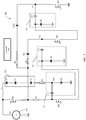
- FIG. 1 depicts a block diagram of a circuit topology driving a set of light emitting diodes according to one or more embodiments.
- the circuit topology 100 includes a controller 102 and a set 104 of light emitting diodes D1, D2, ... D N .
- N represents a positive integer value greater than 2).
- the controller 102 is configured to control the switching elements M1, M2, M3, and M4 in the circuit topology 100. That is to the say, the controller 102 can controller whether any of the switching elements are in an 'On' position or in an 'Off' position.
- the switching elements M1, M2, M3, and M4 are field effect transmitters (FETs) where M2 is a P-MOS type FET and M1, M3, and M4 are each an N-MOS type FETs.
- the set 104 of LEDs (D1, D2, ... D N ) are in series connected to a first node and a second node in the circuit topology 100.
- the first node is also attached to a power supply 106.
- the second node is also attached to a resister R1.
- the resister R1 is a current limiting resister with a resistance value of about 50 ohms to 200 ohms.
- the set 104 of LEDs that are connected in series can be driven by this topology 100 which enables the same current flowing through the set 104 of LEDs, and thus provides a better homogeneity of the LEDs' luminance.
- the circuit topology 100 utilizing lower input voltage and is not limited to the number of LEDs connected.
- the switching elements M1, M2, M3, and M4 will generate a voltage magnitude required to drive the set 104 of LEDs.
- Switching period is controlled, by the controller 102, to regulate the voltage across the charge pump capacitor C1, C2, and C3 based on the desired current.
- a charge pump is a kind of DC to DC converter that uses capacitors for energetic charge storage to raise or lower voltage.
- the system 100 includes three charge pumps 112, 114, 116. These charge pumps 112, 114, 116 will provide an increase (or step-up) in voltage for the system 100. For example, these charge pumps will provide voltage of 1x, 2x, 3x, ... nx (where n is chosen with respect to the switching frequency and the capacitor value in order to supply the required LED current to drive the set 104 of LEDs).
- the controller 102 provides a control voltage for the switching elements M1, M2, M3, and M4 at a predefined switching frequency.
- the switching frequency can be greater than 200Hz so as to avoid human eye visual problems of the LEDs; however, the switching frequency can be lower than 200Hz in some embodiments.
- the controller 102 can be an astable based multi-vibrator having constant t on /t off for fixed brightness or a microcontroller to control duty cycle of the LEDs for dimming.
- the set 104 of LEDs can be any number of LEDs driven by the LED driving circuit. For example, for a set of 10 LEDs with a breakdown voltage of 3.5V each, and a minimum require voltage should be 35V.
- the on/off time of the switching elements M1, M2, M3, and M4 can be controlled, by the controlled 102, to achieve adjustable luminance making dimming on the LEDs, which can be, for example, white LEDs.
- switching elements M1, M3, and M4 are N-MOS type FETs and M2 is a P-MOS type FET which operates as a switch for the charge pump circuits 112, 114, 116.
- the circuit 100 includes the voltage nodes V1, V2, V3, and V4. Vref is taken as reference node to evaluate the charge pumps 112, 114, 116 voltage levels.
- the capacitor C1 provides the first charge pump 112 voltage
- capacitor C2 provides the second charge pump 114 voltage
- capacitor C3 provides the third charge pump 116 voltage.
- the controller 102 can operate the switching elements as follows. At an initial state, switching element M2 is OFF and M1, M3, and M4 are OFF. At this initial state, Vin is much less than the LED set 104 forward bias voltage and therefore the LED set 104 is in an OFF state.
- the controller 102 or any of the hardware referenced in the system 200 can be implemented by executable instructions and/or circuitry such as a processing circuit and memory.
- the processing circuit can be embodied in any type of central processing unit (CPU), including a microprocessor, a digital signal processor (DSP), a microcontroller, an application specific integrated circuit (ASIC), a field programmable gate array (FPGA), or the like.
- the memory may include random access memory (RAM), read only memory (ROM), or other electronic, optical, magnetic, or any other computer readable medium onto which is stored data and algorithms as executable instructions in a non-transitory form.
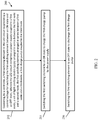
- FIG. 2 depicts a block diagram of a method for operating an LED circuit according to one or more embodiments.
- the method 200 includes operating, by a controller, a first switching element in the LED circuit by providing a control voltage for switching the first switching element between an ON state and an OFF state, wherein the LED circuit comprises a power supply coupled to a first node, a set of light emitting diodes (LEDs) arranged in series between the first node and a second node, the first switching element arranged in series between a first node and a third node, a first charge pump coupled to the third node as shown in block 202.
- the method 200 includes switching the first switching element to an ON state to charge the first charge pump by the power supply.
- the method 200 includes switching the first switching element to an OFF state to discharge the first charge pump.
- FIG. 3 depicts a block diagram of a circuit topology driving a set of light emitting diodes according to one or more embodiments.
- the circuit topology 300 includes resistors R2 and R3 that can be utilized in conjunction with R4 to provide independent current control to each respective capacitors (C1, C2, C3) in the charge pumps 112, 114, 116.
- the charge pumps step up the voltage supplied for the system 300 according to the following described formula.
- a time constant ( ⁇ ) of capacitor can be derived from equation 1.
- Equivalent capacitance during charging phase is the sum of capacitance C1, C2, C3...Cn.
- the voltage across each capacitor is given as equation 2 (previously referenced). I(t) is determined by Vin and R3.
- the capacitor C1, C2, C3, Cn will be in series R1 and LEDs. R1 and number of LEDs will determine the rate at which capacitor to be discharged.
- providing time constant can be described with respect to resistors R2, R3, R4.
- exemplary is used herein to mean “serving as an example, instance or illustration.” Any embodiment or design described herein as “exemplary” is not necessarily to be construed as preferred or advantageous over other embodiments or designs.
- the terms “at least one” and “one or more” may be understood to include any integer number greater than or equal to one, i.e. one, two, three, four, etc.
- the terms “a plurality” may be understood to include any integer number greater than or equal to two, i.e. two, three, four, five, etc.
- connection may include both an indirect “connection” and a direct “connection.”
Landscapes
- Engineering & Computer Science (AREA)
- Power Engineering (AREA)
- Circuit Arrangement For Electric Light Sources In General (AREA)
- Led Devices (AREA)
Abstract
Description
- This application claims the benefit of Indian provisional application no.
201911015618 filed April 18, 2019 - The present invention generally relates to light emitting diodes (LEDs), and more specifically, to circuit and method for driving LEDs and display apparatus.
- A light-emitting diode (LED) circuit (also referred to as an LED driver) is an electrical circuit used for an LED. The circuit provides sufficient current to light the LED at the required brightness, while also limiting the current to prevent damaging the LED.
- The voltage drop across an LED is approximately constant over a wide range of operating current; therefore, a small increase in applied voltage greatly increases the current. Very simple circuits are used for low-power indicator LEDs. More complex, current source circuits are required when driving high-power LEDs for illumination to achieve correct current regulation. LED driving circuits can face drive voltage shortages utilizing conventional LED modules, especially when driving a large number of LEDs connected in series.
- Embodiments of the present invention are directed to system. A non-limiting example of the system includes a set of light emitting diodes (LEDs) arranged in series between a first node and a second node, a power supply coupled to the first node, a first switching element arranged in series between the first node and a third node, wherein the first switching element is in parallel with the set of LEDs, a first charge pump coupled to the third node, a controller configured to operate the first switching element by providing a control voltage for switching the first switching element between an ON and an OFF, wherein the control voltage comprises a switching frequency, and wherein the first charge pump is charged by the power supply responsive to the switching element being in an ON state.
- Embodiments of the present invention are directed to a method for operating an LED circuit. A non-limiting example of the method includes operating, by a controller, a first switching element in the LED circuit by providing a control voltage for switching the first switching element between an ON state and an OFF state, wherein the LED circuit comprises a power supply coupled to a first node, a set of light emitting diodes (LEDs) arranged in series between the first node and a second node, the first switching element arranged in series between a first node and a third node, a first charge pump coupled to the third node, switching the first switching element to an ON state to charge the first charge pump by the power supply.
- Additional technical features and benefits are realized through the techniques of the present invention. Embodiments and aspects of the invention are described in detail herein and are considered a part of the claimed subject matter. For a better understanding, refer to the detailed description and to the drawings.
- The specifics of the exclusive rights described herein are particularly pointed out and distinctly claimed in the claims at the conclusion of the specification. The foregoing and other features and advantages of the embodiments of the invention are apparent from the following detailed description taken in conjunction with the accompanying drawings in which:
-
FIG. 1 depicts a block diagram of a circuit topology driving a set of light emitting diodes according to one or more embodiments; -
FIG. 2 depicts a block diagram of a operating an LED circuit according to one or more embodiments; and -
FIG. 3 depicts a block diagram of a circuit topology driving a set of light emitting diodes according to one or more embodiments. - The diagrams depicted herein are illustrative. There can be many variations to the diagram or the operations described therein without departing from the spirit of the invention. For instance, the actions can be performed in a differing order or actions can be added, deleted or modified. Also, the term "coupled" and variations thereof describes having a communications path between two elements and does not imply a direct connection between the elements with no intervening elements/connections between them. All of these variations are considered a part of the specification.
- Turning now to an overview of technologies that are more specifically relevant to aspects of the invention, LEDs can be utilized in many power sensitive applications such as, for example, displays and low power electronic devices in aircraft lighting systems, aircraft interiors, aircraft display, landing lights, strobe lights for flashing emergency needs, automobiles, and commercial uses. However, as mentioned above, current LED driving circuits suffer from shortages in LED drive voltages and power loss.
- The above-described aspects of the invention address the shortcomings of the prior art by providing an LED driving circuit which yields LED drive more efficiently. Aspects include a circuit topology that can be configured in energy efficient LED applications where power consumption can be an issue. The LED driving circuit described herein drives an array of LEDs by utilizing an inductor/transformer to provide step-up voltage or by utilizing a capacitive multiplier. This LED driving circuit solves the problem of dissipating additional charges in the inrush current limiting resistor during capacitor discharging phase and different step-up voltage levels can be achieved. By this, the power dissipation and efficiency is improved with fewer components than would typically be required.
-
FIG. 1 depicts a block diagram of a circuit topology driving a set of light emitting diodes according to one or more embodiments. Thecircuit topology 100 includes acontroller 102 and aset 104 of light emitting diodes D1, D2, ... DN. (Herein, N represents a positive integer value greater than 2). Thecontroller 102 is configured to control the switching elements M1, M2, M3, and M4 in thecircuit topology 100. That is to the say, thecontroller 102 can controller whether any of the switching elements are in an 'On' position or in an 'Off' position. In one or more embodiments, the switching elements M1, M2, M3, and M4 are field effect transmitters (FETs) where M2 is a P-MOS type FET and M1, M3, and M4 are each an N-MOS type FETs. Theset 104 of LEDs (D1, D2, ... DN) are in series connected to a first node and a second node in thecircuit topology 100. The first node is also attached to apower supply 106. The second node is also attached to a resister R1. In some embodiments, the resister R1 is a current limiting resister with a resistance value of about 50 ohms to 200 ohms. - In one or more embodiments, the
set 104 of LEDs that are connected in series can be driven by thistopology 100 which enables the same current flowing through theset 104 of LEDs, and thus provides a better homogeneity of the LEDs' luminance. By utilizing an LED drive circuit with a ladder charge pump, thecircuit topology 100 utilizing lower input voltage and is not limited to the number of LEDs connected. - In one or more embodiments, the switching elements M1, M2, M3, and M4 will generate a voltage magnitude required to drive the
set 104 of LEDs. Switching period is controlled, by thecontroller 102, to regulate the voltage across the charge pump capacitor C1, C2, and C3 based on the desired current. A charge pump is a kind of DC to DC converter that uses capacitors for energetic charge storage to raise or lower voltage. Thesystem 100 includes threecharge pumps charge pumps system 100. For example, these charge pumps will provide voltage of 1x, 2x, 3x, ... nx (where n is chosen with respect to the switching frequency and the capacitor value in order to supply the required LED current to drive theset 104 of LEDs). - The charge pumps step up the voltage supplied for the
circuit topology 100 according to the following described formula. A time constant (τ) of capacitor can be derived from equation 1. Based on equation 1, the frequency is (f) = 1 / τ. Where, R= R3 and C= C1, C2, C3...Cn. Equivalent capacitance during charging phase is the sum of capacitance C1, C2, C3...Cn. The voltage across each capacitor is given as equation 2. I(t) is determined by Vin and R3. During discharging phase the capacitor C1, C2, C3, Cn will be in series R1 and LEDs. R1 and number of LEDs will determine the rate at which capacitor to be discharged.

- In one or more embodiments, the
controller 102 provides a control voltage for the switching elements M1, M2, M3, and M4 at a predefined switching frequency. The switching frequency can be greater than 200Hz so as to avoid human eye visual problems of the LEDs; however, the switching frequency can be lower than 200Hz in some embodiments. In one or more embodiments, thecontroller 102 can be an astable based multi-vibrator having constant ton/toff for fixed brightness or a microcontroller to control duty cycle of the LEDs for dimming. - In one or more embodiments, the
set 104 of LEDs can be any number of LEDs driven by the LED driving circuit. For example, for a set of 10 LEDs with a breakdown voltage of 3.5V each, and a minimum require voltage should be 35V. Thepower supply 106 for this example can be 15V (i.e., Vin = 15V) and the charge pumps 112, 114, 116 will step up this voltage to 35V where the remaining voltage will drop across the series resistance R1 which provides the controlled current for LED operation. Further, the on/off time of the switching elements M1, M2, M3, and M4 can be controlled, by the controlled 102, to achieve adjustable luminance making dimming on the LEDs, which can be, for example, white LEDs. As shown in the illustrated example, switching elements M1, M3, and M4 are N-MOS type FETs and M2 is a P-MOS type FET which operates as a switch for thecharge pump circuits circuit 100 includes the voltage nodes V1, V2, V3, and V4. Vref is taken as reference node to evaluate the charge pumps 112, 114, 116 voltage levels. The capacitor C1 provides thefirst charge pump 112 voltage, capacitor C2 provides thesecond charge pump 114 voltage, and capacitor C3 provides thethird charge pump 116 voltage. These capacitors C1, C2, C3 are configured to and arranged in thecircuit topology 100 to provide negative voltage with respect to the positive voltage input (Vin). This in turn will sum up with Vin so that the net voltage is Vin = V1 - V2 - V3 - V4. For calculating V1, V1 = Vin + V2 + V3 + V4. - In one or more embodiments, the
controller 102 can operate the switching elements as follows. At an initial state, switching element M2 is OFF and M1, M3, and M4 are OFF. At this initial state, Vin is much less than the LED set 104 forward bias voltage and therefore the LED set 104 is in an OFF state. - In one or more embodiments, when switching element M2 is turned ON and M1, M3, M4 are OFF, as controlled by the
controller 102, capacitors C1, C2, C3 will be charged through diodes D5, D6, and D9. Diodes D8, D10 will provide isolation between the capacitor banks. Then, when switching element M2 is turned OFF and M1, M3, M4 are ON, the capacitors C1, C2, C3 will discharge through M1, M4, M3 switching elements in-series with Vin and theset 104 of LEDs. This causes the net voltage of node V1 to be the sum of the capacitor voltage and input voltage. Also, resistor R3 can have a resistance of any value to limit the inrush current for the charging circuit. For an input voltage Vin = 15V, the voltage is calculated by using Vin = 15V, V2 = 15V, V3 = 15V, V4 = 15V, where V1 = Vin + V2 + V3 + V4 = 60V. - In one or more embodiments, the
controller 102 or any of the hardware referenced in thesystem 200 can be implemented by executable instructions and/or circuitry such as a processing circuit and memory. The processing circuit can be embodied in any type of central processing unit (CPU), including a microprocessor, a digital signal processor (DSP), a microcontroller, an application specific integrated circuit (ASIC), a field programmable gate array (FPGA), or the like. Also, in embodiments, the memory may include random access memory (RAM), read only memory (ROM), or other electronic, optical, magnetic, or any other computer readable medium onto which is stored data and algorithms as executable instructions in a non-transitory form. -
FIG. 2 depicts a block diagram of a method for operating an LED circuit according to one or more embodiments. Themethod 200 includes operating, by a controller, a first switching element in the LED circuit by providing a control voltage for switching the first switching element between an ON state and an OFF state, wherein the LED circuit comprises a power supply coupled to a first node, a set of light emitting diodes (LEDs) arranged in series between the first node and a second node, the first switching element arranged in series between a first node and a third node, a first charge pump coupled to the third node as shown inblock 202. Atblock 204, themethod 200 includes switching the first switching element to an ON state to charge the first charge pump by the power supply. And atblock 206, themethod 200 includes switching the first switching element to an OFF state to discharge the first charge pump. - Additional processes may also be included. It should be understood that the processes depicted in
FIG. 2 represent illustrations, and that other processes may be added or existing processes may be removed, modified, or rearranged without departing from the scope and spirit of the present disclosure. -
FIG. 3 depicts a block diagram of a circuit topology driving a set of light emitting diodes according to one or more embodiments. In addition, since thecircuit topology 300 is similar to that of thesystem 100 according toFIG. 1 , like elements refer to like reference numerals and detailed description thereof is omitted to the extent that the like elements are the same. Thecircuit topology 300 includes resistors R2 and R3 that can be utilized in conjunction with R4 to provide independent current control to each respective capacitors (C1, C2, C3) in the charge pumps 112, 114, 116. As described above, the charge pumps step up the voltage supplied for thesystem 300 according to the following described formula. A time constant (τ) of capacitor can be derived from equation 1. Based on equation 1 (previously referenced), the frequency is (f) = 1 / τ. Where, R= R3 and C= C1, C2, C3...Cn. Equivalent capacitance during charging phase is the sum of capacitance C1, C2, C3...Cn. The voltage across each capacitor is given as equation 2 (previously referenced). I(t) is determined by Vin and R3. During discharging phase the capacitor C1, C2, C3, Cn will be in series R1 and LEDs. R1 and number of LEDs will determine the rate at which capacitor to be discharged. - In one or more embodiments, providing time constant can be described with respect to resistors R2, R3, R4. This resistor arrangement provides independent current control to each capacitor. Thereby if R2 = R3 = R4 and C1 = C2 = C3 then it is possible to charge Vc1 =Vc2 =Vc3 (i.e., same voltage across each capacitor). If resistor R2, R3, R4 are of different values then the charging time will vary for each capacitor; therefore the voltage across each capacitor will vary due to different R2, R3, R4 values. Similarly if C1, C2, C3 of different value and R2 = R3 = R4 then this combination will achieve different voltage levels across each capacitor.
- The term "about" is intended to include the degree of error associated with measurement of the particular quantity based upon the equipment available at the time of filing the application.
- Various embodiments of the invention are described herein with reference to the related drawings. Alternative embodiments of the invention can be devised without departing from the scope of this invention. Various connections and positional relationships (e.g., over, below, adjacent, etc.) are set forth between elements in the following description and in the drawings. These connections and/or positional relationships, unless specified otherwise, can be direct or indirect, and the present invention is not intended to be limiting in this respect. Accordingly, a coupling of entities can refer to either a direct or an indirect coupling, and a positional relationship between entities can be a direct or indirect positional relationship. Moreover, the various tasks and process steps described herein can be incorporated into a more comprehensive procedure or process having additional steps or functionality not described in detail herein.
- The following definitions and abbreviations are to be used for the interpretation of the claims and the specification. As used herein, the terms "comprises," "comprising," "includes," "including," "has," "having," "contains" or "containing," or any other variation thereof, are intended to cover a non-exclusive inclusion. For example, a composition, a mixture, process, method, article, or apparatus that comprises a list of elements is not necessarily limited to only those elements but can include other elements not expressly listed or inherent to such composition, mixture, process, method, article, or apparatus.
- Additionally, the term "exemplary" is used herein to mean "serving as an example, instance or illustration." Any embodiment or design described herein as "exemplary" is not necessarily to be construed as preferred or advantageous over other embodiments or designs. The terms "at least one" and "one or more" may be understood to include any integer number greater than or equal to one, i.e. one, two, three, four, etc. The terms "a plurality" may be understood to include any integer number greater than or equal to two, i.e. two, three, four, five, etc. The term "connection" may include both an indirect "connection" and a direct "connection."
- For the sake of brevity, conventional techniques related to making and using aspects of the invention may or may not be described in detail herein. In particular, various aspects of computing systems and specific computer programs to implement the various technical features described herein are well known. Accordingly, in the interest of brevity, many conventional implementation details are only mentioned briefly herein or are omitted entirely without providing the well-known system and/or process details.
- The terminology used herein is for the purpose of describing particular embodiments only and is not intended to be limiting of the present disclosure. As used herein, the singular forms "a", "an" and "the" are intended to include the plural forms as well, unless the context clearly indicates otherwise. It will be further understood that the terms "comprises" and/or "comprising," when used in this specification, specify the presence of stated features, integers, steps, operations, elements, and/or components, but do not preclude the presence or addition of one or more other features, integers, steps, operations, element components, and/or groups thereof.
- While the present disclosure has been described with reference to an exemplary embodiment or embodiments, it will be understood by those skilled in the art that various changes may be made and equivalents may be substituted for elements thereof without departing from the scope of the present disclosure. In addition, many modifications may be made to adapt a particular situation or material to the teachings of the present disclosure without departing from the essential scope thereof. Therefore, it is intended that the present disclosure not be limited to the particular embodiment disclosed as the best mode contemplated for carrying out this present disclosure, but that the present disclosure will include all embodiments falling within the scope of the claims.
Claims (15)
- A system comprising:
a set of light emitting diodes (LEDs) (104) arranged in series between a first node and a second node;a power supply coupled to the first node;a first switching element arranged in series between the first node and a third node, wherein the first switching element is in parallel with the set of LEDs;a first charge pump coupled to the third node;a controller (102) configured to:operate the first switching element by providing a control voltage for switching the first switching element between an ON and an OFF, wherein the control voltage comprises a switching frequency; andwherein the first charge pump is charged by the power supply responsive to the switching element being in an ON state. - The system of Claim 1, wherein the first charge pump comprises a capacitor and a diode, and preferably wherein a discharge path of the capacitor is in series with the power supply and the set of LEDs.
- The system of claims 1 or 2 further comprising:a second switching element arranged in series between the third node and a fourth node;a second charge pump coupled to the fourth node and a fifth node; andwherein the controller is further configured to:
operate the second switching element by providing the control voltage for switching the second switching element between an OFF and an ON. - The system of claim 3 further comprising:a third switching element arranged in series between the fifth node and a sixth node;a third charge pump coupled to the sixth node and a seventh node; andwherein the controller is further configured to:
operate the third switching element by providing the control voltage for switching the second switching element between an OFF and an ON. - The system of Claim 4 further comprising:a fourth switching element coupled to the seventh node and coupled to ground; andwherein the controller is further configured to:
operate the third switching element by providing the control voltage for switching the second switching element between an OFF and an ON. - The system of any preceding Claim, wherein the first switching element comprises a P-MOS type field effect transistor (FET).
- The system of Claim 3, wherein the second switching element comprises an N-MOS type field effect transistor.
- The system of any preceding Claim, wherein the controller comprises an astable based multi-vibrator; and/or
wherein the switching frequency is about 200 Hertz. - The system of any preceding Claim, wherein the switching frequency is greater than 200 Hertz.
- A method for operating an LED circuit comprising:operating, by a controller, a first switching element in the LED circuit by providing a control voltage for switching the first switching element between an ON state and an OFF state;wherein the LED circuit comprises:a power supply coupled to a first node;a set of light emitting diodes (LEDs) arranged in series between the first node and a second node;the first switching element arranged in series between a first node and a third node;a first charge pump coupled to the third node;switching the first switching element to an ON state to charge the first charge pump by the power supply.
- The method of Claim 10, wherein a discharge path of the capacitor is in series with the power supply and the set of LEDs; and/or
wherein the first charge pump comprises a capacitor and a diode. - The method of Claims 10 or 11, further comprising:
switching the first switching element to an OFF state to discharge the first charge pump. - The method of any of Claims 10 to 12, wherein the LED circuit further comprises:operating a second switching element by providing the control voltage for switching the second switching element between an OFF and an ON; andwherein the LED circuit further comprises:the second switching element arranged in series between the third node and a fourth node;a second charge pump coupled to the fourth node and a fifth node; and
- The method of any of Claims 10 to 13, wherein the first switching element comprises a P-MOS type field effect transistor (FET), and preferably wherein the second switching element comprises an N-MOS type field effect transistor.
- The method of any of Claims 10 to 14, wherein the controller comprises an astable based multi-vibrator; and/or
wherein the switching frequency is greater than 200 Hertz.
Applications Claiming Priority (1)
| Application Number | Priority Date | Filing Date | Title |
|---|---|---|---|
| IN201911015618 | 2019-04-18 |
Publications (1)
| Publication Number | Publication Date |
|---|---|
| EP3726937A1 true EP3726937A1 (en) | 2020-10-21 |
Family
ID=68732954
Family Applications (1)
| Application Number | Title | Priority Date | Filing Date |
|---|---|---|---|
| EP19212574.8A Pending EP3726937A1 (en) | 2019-04-18 | 2019-11-29 | Driving light emitting diodes and display apparatus |
Country Status (2)
| Country | Link |
|---|---|
| US (1) | US10939525B2 (en) |
| EP (1) | EP3726937A1 (en) |
Families Citing this family (1)
| Publication number | Priority date | Publication date | Assignee | Title |
|---|---|---|---|---|
| US12349250B2 (en) * | 2023-01-19 | 2025-07-01 | Goodrich Lighting Systems, Inc. | Night vision imaging system (NVIS) compatible lighting with an adjustable melanopic photopic ratio |
Citations (4)
| Publication number | Priority date | Publication date | Assignee | Title |
|---|---|---|---|---|
| US20070200615A1 (en) * | 2006-02-28 | 2007-08-30 | Jan-Erik Eklund | Driver Circuit |
| US20130175942A1 (en) * | 2011-07-08 | 2013-07-11 | Commissariat A L'energie Atomique Et Aux Ene Alt | Voltage multiplier circuit |
| GB2536851A (en) * | 2013-11-18 | 2016-10-05 | Tridonic Uk Ltd | Driver module for driving LEDs |
| EP3342258A1 (en) * | 2015-12-01 | 2018-07-04 | Philips Lighting Holding B.V. | Coded light modulation arrangement |
Family Cites Families (14)
| Publication number | Priority date | Publication date | Assignee | Title |
|---|---|---|---|---|
| US6628252B2 (en) * | 2000-05-12 | 2003-09-30 | Rohm Co., Ltd. | LED drive circuit |
| JP2002217304A (en) | 2000-11-17 | 2002-08-02 | Rohm Co Ltd | Semiconductor device |
| US6359392B1 (en) | 2001-01-04 | 2002-03-19 | Motorola, Inc. | High efficiency LED driver |
| US6690146B2 (en) | 2002-06-20 | 2004-02-10 | Fairchild Semiconductor Corporation | High efficiency LED driver |
| US7034601B2 (en) | 2003-04-04 | 2006-04-25 | Stmicroelectronics, S.R.L. | Hybrid inductive-capacitive charge pump with high diode driving capability |
| US20060109205A1 (en) | 2004-11-24 | 2006-05-25 | Qi Deng | High Efficiency multi-mode charge pump based LED driver |
| US7271642B2 (en) | 2005-12-27 | 2007-09-18 | Aimtron Technology Corp. | Charge pump drive circuit for a light emitting diode |
| WO2010022350A2 (en) * | 2008-08-21 | 2010-02-25 | Asic Advantage Inc. | Light emitting diode fault monitoring |
| EP2410819A1 (en) | 2010-07-23 | 2012-01-25 | ST-Ericsson SA | Circuit for retro-lighting a display |
| JP5842090B2 (en) * | 2010-08-25 | 2016-01-13 | パナソニックIpマネジメント株式会社 | Illumination light communication device |
| KR101208576B1 (en) | 2010-08-25 | 2012-12-06 | 주식회사 동부하이텍 | luminous device drive apparatus |
| CN101969720B (en) * | 2010-09-15 | 2013-09-18 | 成都芯源系统有限公司 | LED bypass control circuit and control method |
| CN105706528B (en) | 2013-09-19 | 2018-06-08 | 飞利浦照明控股有限公司 | LED drive with differential voltage source |
| WO2018064655A1 (en) * | 2016-09-30 | 2018-04-05 | Edward Stoneham | Apparatus and methods for controlling led light flux |
-
2019
- 2019-06-19 US US16/445,349 patent/US10939525B2/en active Active
- 2019-11-29 EP EP19212574.8A patent/EP3726937A1/en active Pending
Patent Citations (4)
| Publication number | Priority date | Publication date | Assignee | Title |
|---|---|---|---|---|
| US20070200615A1 (en) * | 2006-02-28 | 2007-08-30 | Jan-Erik Eklund | Driver Circuit |
| US20130175942A1 (en) * | 2011-07-08 | 2013-07-11 | Commissariat A L'energie Atomique Et Aux Ene Alt | Voltage multiplier circuit |
| GB2536851A (en) * | 2013-11-18 | 2016-10-05 | Tridonic Uk Ltd | Driver module for driving LEDs |
| EP3342258A1 (en) * | 2015-12-01 | 2018-07-04 | Philips Lighting Holding B.V. | Coded light modulation arrangement |
Also Published As
| Publication number | Publication date |
|---|---|
| US20200337125A1 (en) | 2020-10-22 |
| US10939525B2 (en) | 2021-03-02 |
Similar Documents
| Publication | Publication Date | Title |
|---|---|---|
| KR101910669B1 (en) | Control circuit of switching power supply for driving light emitting elements, and light emitting device and electronic apparatus using the same | |
| US10187938B2 (en) | Multichannel constant current LED controlling circuit and controlling method | |
| US10396659B2 (en) | Load driving device, and lighting apparatus and liquid crystal display device using the same | |
| CN102598315B (en) | Driving circuit and driving method of light-emitting diode string for backlight, and backlight and display device using the same | |
| TWI434609B (en) | Led driver circuit | |
| US20150257225A1 (en) | Ac-powered led light engines, integrated circuits and illuminating apparatuses having the same | |
| CN102821511B (en) | Led drive circuit | |
| JP2012095518A (en) | Load drive circuit, light emitting device and display device using the same | |
| EP2209353A2 (en) | Light source driving apparatus | |
| JP5530489B2 (en) | LED protection circuit | |
| US11523481B2 (en) | Combinational circuit and control circuit | |
| JP5960982B2 (en) | Control circuit for switching power supply for driving light emitting element, and light emitting device and electronic device using the same | |
| TW201228453A (en) | Full function LED driver for LCD backlighting | |
| KR101932364B1 (en) | Led backlight for liquid crystal display device and liquid crystal display device | |
| US10939525B2 (en) | Driving light emitting diodes and display apparatus | |
| KR101932366B1 (en) | Led backlight source for liquid crystal display device and liquid crystal display device | |
| US9306383B2 (en) | Low current protection circuit | |
| CN113841336A (en) | Negative voltage rail | |
| JP6247455B2 (en) | LIGHT EMITTING ELEMENT DRIVE CIRCUIT, AND LIGHT EMITTING DEVICE AND ELECTRONIC DEVICE USING THE SAME | |
| US10582577B2 (en) | LED drive circuit | |
| EP3214904B1 (en) | Wled driver and driving control method | |
| EP4344356A1 (en) | Light-emitting diode driving device with adjustable dimming depth | |
| EP2814159B1 (en) | Power supply circuit | |
| CN110390913B (en) | Driving circuit, backlight system and display device | |
| US10827585B1 (en) | Driving light emitting diodes and display apparatus |
Legal Events
| Date | Code | Title | Description |
|---|---|---|---|
| PUAI | Public reference made under article 153(3) epc to a published international application that has entered the european phase |
Free format text: ORIGINAL CODE: 0009012 |
|
| STAA | Information on the status of an ep patent application or granted ep patent |
Free format text: STATUS: THE APPLICATION HAS BEEN PUBLISHED |
|
| AK | Designated contracting states |
Kind code of ref document: A1 Designated state(s): AL AT BE BG CH CY CZ DE DK EE ES FI FR GB GR HR HU IE IS IT LI LT LU LV MC MK MT NL NO PL PT RO RS SE SI SK SM TR |
|
| AX | Request for extension of the european patent |
Extension state: BA ME |
|
| STAA | Information on the status of an ep patent application or granted ep patent |
Free format text: STATUS: REQUEST FOR EXAMINATION WAS MADE |
|
| 17P | Request for examination filed |
Effective date: 20210420 |
|
| RBV | Designated contracting states (corrected) |
Designated state(s): AL AT BE BG CH CY CZ DE DK EE ES FI FR GB GR HR HU IE IS IT LI LT LU LV MC MK MT NL NO PL PT RO RS SE SI SK SM TR |
|
| STAA | Information on the status of an ep patent application or granted ep patent |
Free format text: STATUS: EXAMINATION IS IN PROGRESS |
|
| 17Q | First examination report despatched |
Effective date: 20230103 |