EP3726675A1 - Semiconductor laser device, and method and program for driving semiconductor laser device - Google Patents
Semiconductor laser device, and method and program for driving semiconductor laser device Download PDFInfo
- Publication number
- EP3726675A1 EP3726675A1 EP18887596.7A EP18887596A EP3726675A1 EP 3726675 A1 EP3726675 A1 EP 3726675A1 EP 18887596 A EP18887596 A EP 18887596A EP 3726675 A1 EP3726675 A1 EP 3726675A1
- Authority
- EP
- European Patent Office
- Prior art keywords
- temperature
- semiconductor laser
- control part
- temperature control
- supply signal
- Prior art date
- Legal status (The legal status is an assumption and is not a legal conclusion. Google has not performed a legal analysis and makes no representation as to the accuracy of the status listed.)
- Pending
Links
Images


Classifications
-
- H—ELECTRICITY
- H01—ELECTRIC ELEMENTS
- H01S—DEVICES USING THE PROCESS OF LIGHT AMPLIFICATION BY STIMULATED EMISSION OF RADIATION [LASER] TO AMPLIFY OR GENERATE LIGHT; DEVICES USING STIMULATED EMISSION OF ELECTROMAGNETIC RADIATION IN WAVE RANGES OTHER THAN OPTICAL
- H01S5/00—Semiconductor lasers
- H01S5/06—Arrangements for controlling the laser output parameters, e.g. by operating on the active medium
- H01S5/0607—Arrangements for controlling the laser output parameters, e.g. by operating on the active medium by varying physical parameters other than the potential of the electrodes, e.g. by an electric or magnetic field, mechanical deformation, pressure, light, temperature
- H01S5/0612—Arrangements for controlling the laser output parameters, e.g. by operating on the active medium by varying physical parameters other than the potential of the electrodes, e.g. by an electric or magnetic field, mechanical deformation, pressure, light, temperature controlled by temperature
-
- H—ELECTRICITY
- H01—ELECTRIC ELEMENTS
- H01S—DEVICES USING THE PROCESS OF LIGHT AMPLIFICATION BY STIMULATED EMISSION OF RADIATION [LASER] TO AMPLIFY OR GENERATE LIGHT; DEVICES USING STIMULATED EMISSION OF ELECTROMAGNETIC RADIATION IN WAVE RANGES OTHER THAN OPTICAL
- H01S5/00—Semiconductor lasers
- H01S5/02—Structural details or components not essential to laser action
- H01S5/024—Arrangements for thermal management
- H01S5/02407—Active cooling, e.g. the laser temperature is controlled by a thermo-electric cooler or water cooling
- H01S5/02415—Active cooling, e.g. the laser temperature is controlled by a thermo-electric cooler or water cooling by using a thermo-electric cooler [TEC], e.g. Peltier element
-
- H—ELECTRICITY
- H01—ELECTRIC ELEMENTS
- H01S—DEVICES USING THE PROCESS OF LIGHT AMPLIFICATION BY STIMULATED EMISSION OF RADIATION [LASER] TO AMPLIFY OR GENERATE LIGHT; DEVICES USING STIMULATED EMISSION OF ELECTROMAGNETIC RADIATION IN WAVE RANGES OTHER THAN OPTICAL
- H01S5/00—Semiconductor lasers
- H01S5/06—Arrangements for controlling the laser output parameters, e.g. by operating on the active medium
- H01S5/068—Stabilisation of laser output parameters
- H01S5/06804—Stabilisation of laser output parameters by monitoring an external parameter, e.g. temperature
-
- H—ELECTRICITY
- H01—ELECTRIC ELEMENTS
- H01S—DEVICES USING THE PROCESS OF LIGHT AMPLIFICATION BY STIMULATED EMISSION OF RADIATION [LASER] TO AMPLIFY OR GENERATE LIGHT; DEVICES USING STIMULATED EMISSION OF ELECTROMAGNETIC RADIATION IN WAVE RANGES OTHER THAN OPTICAL
- H01S5/00—Semiconductor lasers
- H01S5/06—Arrangements for controlling the laser output parameters, e.g. by operating on the active medium
- H01S5/068—Stabilisation of laser output parameters
- H01S5/0683—Stabilisation of laser output parameters by monitoring the optical output parameters
- H01S5/06837—Stabilising otherwise than by an applied electric field or current, e.g. by controlling the temperature
-
- H—ELECTRICITY
- H01—ELECTRIC ELEMENTS
- H01S—DEVICES USING THE PROCESS OF LIGHT AMPLIFICATION BY STIMULATED EMISSION OF RADIATION [LASER] TO AMPLIFY OR GENERATE LIGHT; DEVICES USING STIMULATED EMISSION OF ELECTROMAGNETIC RADIATION IN WAVE RANGES OTHER THAN OPTICAL
- H01S5/00—Semiconductor lasers
- H01S5/06—Arrangements for controlling the laser output parameters, e.g. by operating on the active medium
- H01S5/068—Stabilisation of laser output parameters
- H01S5/0683—Stabilisation of laser output parameters by monitoring the optical output parameters
- H01S5/0687—Stabilising the frequency of the laser
-
- H—ELECTRICITY
- H01—ELECTRIC ELEMENTS
- H01S—DEVICES USING THE PROCESS OF LIGHT AMPLIFICATION BY STIMULATED EMISSION OF RADIATION [LASER] TO AMPLIFY OR GENERATE LIGHT; DEVICES USING STIMULATED EMISSION OF ELECTROMAGNETIC RADIATION IN WAVE RANGES OTHER THAN OPTICAL
- H01S5/00—Semiconductor lasers
- H01S5/10—Construction or shape of the optical resonator, e.g. extended or external cavity, coupled cavities, bent-guide, varying width, thickness or composition of the active region
- H01S5/12—Construction or shape of the optical resonator, e.g. extended or external cavity, coupled cavities, bent-guide, varying width, thickness or composition of the active region the resonator having a periodic structure, e.g. in distributed feedback [DFB] lasers
-
- G—PHYSICS
- G01—MEASURING; TESTING
- G01N—INVESTIGATING OR ANALYSING MATERIALS BY DETERMINING THEIR CHEMICAL OR PHYSICAL PROPERTIES
- G01N21/00—Investigating or analysing materials by the use of optical means, i.e. using sub-millimetre waves, infrared, visible or ultraviolet light
- G01N21/17—Systems in which incident light is modified in accordance with the properties of the material investigated
- G01N21/25—Colour; Spectral properties, i.e. comparison of effect of material on the light at two or more different wavelengths or wavelength bands
- G01N21/31—Investigating relative effect of material at wavelengths characteristic of specific elements or molecules, e.g. atomic absorption spectrometry
- G01N21/39—Investigating relative effect of material at wavelengths characteristic of specific elements or molecules, e.g. atomic absorption spectrometry using tunable lasers
- G01N2021/396—Type of laser source
- G01N2021/399—Diode laser
-
- G—PHYSICS
- G01—MEASURING; TESTING
- G01N—INVESTIGATING OR ANALYSING MATERIALS BY DETERMINING THEIR CHEMICAL OR PHYSICAL PROPERTIES
- G01N21/00—Investigating or analysing materials by the use of optical means, i.e. using sub-millimetre waves, infrared, visible or ultraviolet light
- G01N21/01—Arrangements or apparatus for facilitating the optical investigation
- G01N21/03—Cuvette constructions
- G01N21/031—Multipass arrangements
-
- G—PHYSICS
- G01—MEASURING; TESTING
- G01N—INVESTIGATING OR ANALYSING MATERIALS BY DETERMINING THEIR CHEMICAL OR PHYSICAL PROPERTIES
- G01N21/00—Investigating or analysing materials by the use of optical means, i.e. using sub-millimetre waves, infrared, visible or ultraviolet light
- G01N21/17—Systems in which incident light is modified in accordance with the properties of the material investigated
- G01N21/25—Colour; Spectral properties, i.e. comparison of effect of material on the light at two or more different wavelengths or wavelength bands
- G01N21/31—Investigating relative effect of material at wavelengths characteristic of specific elements or molecules, e.g. atomic absorption spectrometry
- G01N21/35—Investigating relative effect of material at wavelengths characteristic of specific elements or molecules, e.g. atomic absorption spectrometry using infrared light
- G01N21/3504—Investigating relative effect of material at wavelengths characteristic of specific elements or molecules, e.g. atomic absorption spectrometry using infrared light for analysing gases, e.g. multi-gas analysis
-
- G—PHYSICS
- G01—MEASURING; TESTING
- G01N—INVESTIGATING OR ANALYSING MATERIALS BY DETERMINING THEIR CHEMICAL OR PHYSICAL PROPERTIES
- G01N2201/00—Features of devices classified in G01N21/00
- G01N2201/06—Illumination; Optics
- G01N2201/061—Sources
- G01N2201/06113—Coherent sources; lasers
- G01N2201/0612—Laser diodes
-
- H—ELECTRICITY
- H01—ELECTRIC ELEMENTS
- H01S—DEVICES USING THE PROCESS OF LIGHT AMPLIFICATION BY STIMULATED EMISSION OF RADIATION [LASER] TO AMPLIFY OR GENERATE LIGHT; DEVICES USING STIMULATED EMISSION OF ELECTROMAGNETIC RADIATION IN WAVE RANGES OTHER THAN OPTICAL
- H01S5/00—Semiconductor lasers
- H01S5/30—Structure or shape of the active region; Materials used for the active region
- H01S5/34—Structure or shape of the active region; Materials used for the active region comprising quantum well or superlattice structures, e.g. single quantum well [SQW] lasers, multiple quantum well [MQW] lasers or graded index separate confinement heterostructure [GRINSCH] lasers
- H01S5/3401—Structure or shape of the active region; Materials used for the active region comprising quantum well or superlattice structures, e.g. single quantum well [SQW] lasers, multiple quantum well [MQW] lasers or graded index separate confinement heterostructure [GRINSCH] lasers having no PN junction, e.g. unipolar lasers, intersubband lasers, quantum cascade lasers
- H01S5/3402—Structure or shape of the active region; Materials used for the active region comprising quantum well or superlattice structures, e.g. single quantum well [SQW] lasers, multiple quantum well [MQW] lasers or graded index separate confinement heterostructure [GRINSCH] lasers having no PN junction, e.g. unipolar lasers, intersubband lasers, quantum cascade lasers intersubband lasers, e.g. transitions within the conduction or valence bands
-
- H—ELECTRICITY
- H01—ELECTRIC ELEMENTS
- H01S—DEVICES USING THE PROCESS OF LIGHT AMPLIFICATION BY STIMULATED EMISSION OF RADIATION [LASER] TO AMPLIFY OR GENERATE LIGHT; DEVICES USING STIMULATED EMISSION OF ELECTROMAGNETIC RADIATION IN WAVE RANGES OTHER THAN OPTICAL
- H01S5/00—Semiconductor lasers
- H01S5/30—Structure or shape of the active region; Materials used for the active region
- H01S5/34—Structure or shape of the active region; Materials used for the active region comprising quantum well or superlattice structures, e.g. single quantum well [SQW] lasers, multiple quantum well [MQW] lasers or graded index separate confinement heterostructure [GRINSCH] lasers
- H01S5/343—Structure or shape of the active region; Materials used for the active region comprising quantum well or superlattice structures, e.g. single quantum well [SQW] lasers, multiple quantum well [MQW] lasers or graded index separate confinement heterostructure [GRINSCH] lasers in AIIIBV compounds, e.g. AlGaAs-laser, InP-based laser
- H01S5/34313—Structure or shape of the active region; Materials used for the active region comprising quantum well or superlattice structures, e.g. single quantum well [SQW] lasers, multiple quantum well [MQW] lasers or graded index separate confinement heterostructure [GRINSCH] lasers in AIIIBV compounds, e.g. AlGaAs-laser, InP-based laser with a well layer having only As as V-compound, e.g. AlGaAs, InGaAs
Definitions
- the present invention relates to a semiconductor laser device, a method for driving a semiconductor laser device, and a program for driving a semiconductor laser device.
- the gas analyzer includes the semiconductor laser device that emits a laser light having an oscillation wavenumber according to an absorption wavenumber of the measurement target component.
- the oscillation wavenumber is designed with an accuracy of an absorption wavenumber of ⁇ 1 cm -1 . Because the oscillation wavenumber is changed depending on an operating temperature of the semiconductor laser device, the semiconductor laser device is controlled so that variations in oscillation wavenumber of the laser light fall within ⁇ 0.01 cm -1 by temperature control of the semiconductor laser device. In one which is designed to sweep the oscillation wavenumber of the laser light with respect to a predetermined central wavenumber, control is made so that variations in the central wavenumber falls within ⁇ 0.01 cm -1 .
- a semiconductor laser element to emit laser light has conventionally been mounted on a cooling module including a Peltier element in order to perform the temperature control.
- a supply power to the Peltier element is controlled using a detected temperature obtained from a temperature sensor mounted on the cooling module.
- the operating temperature of the semiconductor laser element is adjusted to control so that the variations in the oscillation wavenumber of the laser light falls within ⁇ 0.01 cm -1 .
- the temperature of the semiconductor laser element may not necessarily be identical with the detected temperature obtained from the temperature sensor even if the temperature control is performed using the detected temperature obtained from the temperature sensor. Specifically, even though the temperature sensor is subject to temperature control using the Peltier element, the temperature of the semiconductor laser element may be changed due to a circumferential temperature change. Consequently, variations larger than ⁇ 0.01 cm -1 may occur in the oscillation wavenumber of the laser light.
- Patent Document 1 Japanese Unexamined Patent Publication No. 2009-216385
- the present invention has been made to solve the above problem and has for its main object to ensure that the oscillation wavenumber of the semiconductor laser element is less likely to vary under the influence of the circumferential temperature.
- a semiconductor laser device in one of embodiments of the present invention includes a semiconductor laser element, a temperature control part to control a temperature of the semiconductor laser element, a temperature sensor to detect a temperature of the temperature control part, and a temperature control device to control a supply signal to the temperature control part so that a detected temperature obtained from the temperature sensor reaches a predetermined target temperature.
- the temperature control device changes a target temperature for the temperature control part depending on a supply signal to the temperature control part.
- a supply current, a supply voltage or a supply power is usable as a supply signal to the temperature control part.
- the temperature control device changes the target temperature for the temperature control part depending on the supply signal to the temperature control part, and the temperature of the semiconductor laser element is therefore less likely to change due to a circumferential temperature change, and the oscillation wavenumber of the semiconductor laser element is therefore less likely to vary under the influence of the circumferential temperature.
- the temperature control device preferably includes a relationship data storage part, a supply signal acquisition part and a supply control part.
- the relationship data storage part stores therein relationship data indicating a relationship between a supply signal to the temperature control part and a target temperature for the temperature control part.
- the supply signal acquisition part acquires a supply signal to the temperature control part.
- the supply control part acquires a target temperature for the temperature control part from the relationship data depending on the supply signal thus acquired, and controls the supply signal to the temperature control part so as to achieve the target temperature thus acquired.
- the supply control part When controlling the temperature control part, it is conceivable that the supply signal varies slightly even in a stable state of the temperature control part. In this case, the target temperature may be changed in spite of that no circumferential temperature change occurs.
- the supply control part preferably acquires a target temperature for the temperature control part from the relationship data depending on an average value of the supply signal thus obtained, per predetermined period.
- the supply control part preferably does not change a target temperature for the temperature control part if a variation width of the average value of the supply signal thus obtained is less than a predetermined value.
- the relationship data storage part stores therein relationship data indicating a relationship between a supply signal to the temperature control part and a target temperature for the temperature control part per oscillation wavenumber of the semiconductor laser.
- a method for driving a semiconductor laser device is intended to be applied to a semiconductor laser device.
- the semiconductor laser device includes a semiconductor laser element, a temperature control part to control a temperature of the semiconductor laser element, and a temperature sensor to detect a temperature of the temperature control part.
- the method includes controlling a supply signal to the temperature control part so that a detected temperature obtained from the temperature sensor reaches a predetermined target temperature.
- the method includes changing a target temperature for the temperature control part depending on a supply signal to the temperature control part.
- a driving program is used for a semiconductor laser device.
- the semiconductor laser device includes a semiconductor laser element, a temperature control part to control a temperature of the semiconductor laser element, a temperature sensor to detect a temperature of the temperature control part, and a control device to control a supply signal to the temperature control part so that a detected temperature obtained from the temperature sensor reaches a predetermined target temperature.
- the driving program causes the control device to perform a function of changing a target temperature for the control temperature part depending on a supply signal to the temperature control part.
- the oscillation wavenumber of the semiconductor laser element is less likely to vary under the influence of the circumferential temperature because the target temperature of the temperature control part is changed depending on the supply signal to the temperature control part.
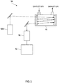
- the semiconductor laser device 100 in the embodiment is intended to be used for a gas analyzer 10 that analyzes a measurement target component in exhaust gas discharged from, for example, an internal combustion engine or an external combustion engine, and in atmosphere as illustrated in FIG. 1 .
- the gas analyzer 10 includes a multiple reflection type measurement cell 11 to permit introduction of the exhaust gas, the semiconductor laser device 100 to emit a laser light to the measurement cell 11, a photodetector 12 to detect the laser light after passing through the measurement cell 11, and an analysis part 13 to analyze the measurement target component by using a detection signal obtained from the photodetector 12.
- the semiconductor laser device 100 is designed to emit a laser light having an oscillation wavenumber of approximately ⁇ 1 cm -1 with respect to an absorption wavenumber of the measurement target component.
- the semiconductor laser device 100 includes a semiconductor laser element 2, a temperature control module 3 to control a temperature of the semiconductor laser element 2, a temperature sensor 4 disposed in the temperature control module 3, and a temperature control device 5 to control the temperature control module 3 on the basis of a detected temperature obtained from the temperature sensor 4.
- the semiconductor laser element 2 is, for example, a quantum cascade laser (QCL) element, and oscillates laser lights of, for example, mid-infrared (4-10 ⁇ m).
- the semiconductor laser element 2 is capable of modulating (changing) an oscillation wavenumber (oscillation wavelength) depending on an applied current (or voltage).
- the semiconductor laser element 2 is subject to current (voltage) control by the laser control device 6.
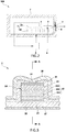
- the semiconductor laser element 2 is, for example, a distributed feedback laser (DFB laser), and includes an optical waveguide 2A composed of a clad layer and a core layer, each disposed on a semiconductor substrate 20 as illustrated in FIGs. 3 and 4 .
- Alight passes through the core layer due to a difference between a refractive index of the clad layer and a refractive index of the core layer in the optical waveguide 3A.
- DFB laser distributed feedback laser
- the semiconductor laser element 2 is one in which a buffer layer 21, a core layer 22, an upper clad layer 23 and a cap layer 24 are formed in this order on an upper surface of the semiconductor substrate 20. These layers 21 to 24 are individually extended in an identical direction.
- the optical waveguide 2A extended in one direction can be formed by causing side surfaces of these layers in their width direction to be covered with a protection film 25.
- the protection film 25 is an inorganic film and may be composed of, for example, SiO 2 or a combination of SiO 2 and Si 3 N 4 .
- the buffer layer 21 and the upper clad layer 23 are layers, each composed of InP.
- a lower clad layer composed of InP may be disposed between the buffer layer 21 and the core layer 22.
- the buffer layer 21 may serve as a clad layer.
- the cap layer 24 is a layer composed of InGaAs, and a part of an upper surface of the layer (both sides in a width direction) is covered with the protection layer 25. Other parts of the upper surface of the cap layer 24 (a middle part in the width direction) are covered with an upper electrode 26.
- the core layer 22 includes a lower guide layer 221 composed of InGaAs, an active layer 222 that emits light upon current injection, and an upper guide layer 223 composed of InGaAs.
- the active layer 222 is composed of a multi quantum well structure including a plurality of well layers, in which a plurality of semiconductor layers serving as a light-emitting region and a plurality of semiconductor layers serving an injection region are alternately laminated one upon another. These well layers may be different in thickness.
- the semiconductor layer serving as the light-emitting region is formed by alternately laminating InGaAs and InAlAs.
- the semiconductor layer serving as the injection region is formed by alternately laminating InGaAs and InAlAs.
- a semiconductor layer element part thus configured is a quantum cascade laser, in which a plurality of cell layers are subjected to multistage connection as illustrated in FIG. 5 , is designed to emit a light by optical transition between subbands formed in quantum cells.
- the semiconductor laser 2 may be a distributed bragg reflector laser (DBR laser).
- a diffraction grating 2B is formed between the core layer 22 and the upper clad layer 23, namely, on the upper guide layer 223 in the semiconductor laser element 2 (refer to FIG. 4 ).
- the diffraction grating 2B is composed of concave parts and convex parts alternately formed on the upper guide layer 223, and the concave parts and the convex parts are extended in a width direction of the upper guide layer 223.
- Lights having a predetermined oscillation wavenumber are mutually intensified and selectively amplified by the diffraction grating 2B.
- the predetermined oscillation wavenumber is prescribed by a pitch of the diffraction grating 2B.
- a lower electrode 37 is disposed on a lower surface of the semiconductor substrate 20.
- a laser light having a predetermined oscillation wavenumber prescribed by the diffraction grating 2B is emitted by applying a current (voltage) for laser oscillation to an upper upper electrode 26 and a lower electrode 27.
- a current source (or voltage source) is coupled to the upper electrode 26 and the lower electrode 27 that are intended for laser oscillation, and the laser control device 8 controls the current source (voltage source).
- the laser control device 6 is designed to control the current source (or voltage source) of the semiconductor laser element 2 by outputting a current (voltage) control signal. Specifically, the laser control device 6 controls the current source (or voltage source) of the semiconductor laser element 2 by outputting a current (or voltage) control signal, thereby causing the semiconductor laser element 2 to be subjected to continuous wave operation (CW) or pulse-like oscillation (pulse driving).
- CW continuous wave operation
- pulse driving pulse-like oscillation
- Ones which cause the pulse driving include pseudo continuous wave operation (pseudo CW).
- the temperature control module 3 includes a substrate 31 having the semiconductor laser element 2 mounted on one surface thereof, namely, a front surface thereof, and a Peltier element 32 that is a temperature control part whose endothermic surface is contactedly disposed on the other surface, namely, rear surface of the substrate 31.
- the Peltier element 32 is a semiconductor element capable of controlling heat generation and heat absorption by using current.
- the Peltier element 32 has such a configuration that a plurality of alternately disposed N-type semiconductors and P-type semiconductors are connected in series by using a metal electrode, and they are held between a pair of ceramic substrates.
- the temperature control module 3 may not include the substrate 31, but may include a semiconductor laser element mounted on the ceramic substrate on a heat absorption side of the Peltier element 32.
- As a temperature control part it is possible to employ, for example, one which uses a compressor, one which uses a heating wire, one which uses a fan, or one which employs a water-cooled system.
- the temperature sensor 4 is disposed on a surface of the substrate 31 and intended to detect a temperature of the substrate 31 with the semiconductor laser element 2 mounted thereon.
- the temperature sensor 4 is, for example, a thermistor. Although the temperature sensor 4 is disposed away from the semiconductor laser element 2 in the embodiment, the temperature sensor 4 may be disposed in contact with the semiconductor laser element 2.
- the semiconductor laser element 2 and the cooling module 3 are accommodated in a tight container 7 in the embodiment.
- Alight outlet part 71 through which a laser light passes to the outside, is formed at a part of the tight container 7 which is opposed to a light emission part of the semiconductor laser element 2.
- An optical window member 8 is disposed on the light outlet part 71, and the optical window member 8 is inclined slightly (for example, 2 degrees) in order to prevent a laser light reflected from the optical window member 8 from returning to the semiconductor laser element 2.
- Alight emitting module is constituted by the tight container 7 accommodating therein the semiconductor laser element 2 and the cooling module 3 or the like.
- the temperature control device 5 is intended to perform feedback control of a supply current, a supply voltage or a supply power to the Peltier element 32 on the basis of a detected temperature obtained from the temperature sensor 4. Specifically, the temperature control device 5 controls the current source (voltage source) of the Peltier element 32 by outputting a current (or voltage) control signal.
- the temperature control device 5 is a general-purpose or special-purpose computer including, as a structure thereof, CPU, memory, input/output interface and AD converter.
- the temperature control device 5 controls a supply power to the Peltier element 32 by causing the CPU and peripheral devices thereof to operate according to a driving program stored in the memory.
- the temperature control device 5 includes a relationship data storage part 51, a supply data acquisition part 52 and a supply control part 53 as illustrated in FIG. 6 .
- the relationship data storage part 51 stores therein relationship data indicating a relationship between a target temperature for the temperature sensor 4 and a supply power to the Peltier element 32 if an oscillation wavenumber of the semiconductor laser element 2 is made constant.
- the supply data acquisition part 52 acquires supply data indicating a supply power to the Peltier element 32.
- the supply control part 53 performs feedback control of the supply power to the Peltier element 32.
- the relationship data storage part 51 stores therein relationship data indicating a relationship between a target temperature T for the temperature sensor 4 and a supply power P to the Peltier element 32 if the oscillation wavenumber (oscillation wavelength ⁇ 1 ) of the semiconductor laser element 2 is made constant.
- a method for generating the relationship data is, for example, as follows.
- a light-emitting module of the semiconductor laser device 100 as a specimen is accommodated in a thermostatic container (not illustrated), and circumferential temperatures (ambient temperatures) are changed, for example, from 5°C to 45°C.
- the Peltier element 32 is controlled so that the oscillation wavelength of the semiconductor laser element 2 becomes constant ( ⁇ 1 ) at the above circumferential temperatures.
- a detected temperature obtained from the Peltier element 32 when the oscillation wavelength of the semiconductor laser element 2 became constant ( ⁇ 1 ) at the individual circumferential temperature and a supply power at that time are recorded.
- a supply current and a supply voltage, each supplied to the Peltier element 32, are detected, and the supply power is calculated from the supply current and the supply voltage.
- the relationship data indicating this relationship is stored in the relationship data storage part 51.
- relationship data relating not only a single oscillation wavelength ( ⁇ 1 ) but also a different oscillation wavelength ( ⁇ 2)
- ⁇ 2 a different oscillation wavelength
- the number of the relationship data is not limited to two, but it may be configured to have relationship data respectively relating to a plurality of oscillation wavelengths.
- a circumferential temperature is detectable from a supply power by linking the circumferential temperature to the relationship data. That is, the Peltier element 32 is usable as a circumferential temperature sensor.
- the supply data acquisition part 52 is designed to acquire a supply current and a supply voltage supplied to the Peltier element 32 and then calculate a supply power by using the supply current and the supply voltage in a state in which the Peltier element 32 is controlled so that a detected temperature obtained from the temperature sensor 4 reaches a constant target temperature.
- the supply current supplied to the Peltier element 32 is detected by a current sensor, and the supply voltage is detected by a voltage sensor. If the Peltier element 32 is subjected to current control, a setting value for the current control is usable. If the Peltier element 32 is subjected to voltage control, a setting value of the voltage control is usable.
- the supply data acquisition part 52 outputs the calculated supply power data to the supply control part 53.
- the supply control part 53 receives the relationship data from the relationship data storage part 51, and also receives the supply power data from the supply data acquisition part 52. Then, the supply control part 53 changes a target temperature for the temperature sensor 4 so that the oscillation wavenumber (oscillation wavelength), from the supply power data and the relationship data. The supply control part 53 then controls a supply power to the Peltier element 32 so that the detected temperature obtained from the temperature sensor 4 reaches a target temperature after being changed.
- the supply control part 53 is designed not to change the target temperature for the Peltier element 32 if a variation range of the acquired supply power is less than a predetermined value.
- predetermined value denotes a threshold value for distinguishing a variation width of the supply power generated in a state in which the Peltier element 32 is controlled so as to achieve the target temperature when no circumferential temperature occurs, and a variation width of a supply power which occurs when a circumferential temperature change occurs.
- the semiconductor laser element 2 is oscillated in a situation where a circumferential temperature (ambient temperature) is 27°C, and the Peltier element 32 is controlled so that a detected temperature obtained from the temperature sensor 4 reaches 25.0 °C. It is also supposed that an actual temperature of the semiconductor laser element 2 is, for example, 70.0 °C.
- the laser control device 6 controls a current (or voltage) applied to the semiconductor laser element 2 so as to cause the semiconductor laser element 2 to emit a laser light having a predetermined wavenumber (predetermined wavelength) (refer to FIG. 7(1) ).
- the temperature control device 5 controls the Peltier element 32 so that a detected temperature obtained from the temperature sensor 4 reaches 25°C. At this point, a supply power to the Peltier element 32 is increased due to a circumferential temperature change, and the semiconductor laser element 2 is excessively cooled and changed to, for example, 69.6°C.
- the oscillation wavenumber (oscillation wavelength) varies accordingly (refer to FIG. 7(2) ).
- the supply data acquisition part 52 of the temperature control device 5 acquires supply power data for the Peltier element 32.
- the supply control part 53 of the temperature control device 5 changes a target temperature so that the oscillation wavenumber (oscillation wavelength) of the semiconductor laser element 2 becomes constant, from the supply power data and the relationship data. For example, the target temperature for the temperature sensor 4 is changed to 24.5°C.
- the supply control part 53 therefore controls a supply power to the Peltier element 32 so that the detected temperature obtained from the temperature sensor 4 reaches 24.5°C.
- the oscillation wavenumber of the semiconductor laser element 2 is less likely to vary under the influence of a circumferential temperature. This is because a target temperature is changed so that the oscillation wavenumber of the semiconductor laser element 2 becomes constant by using the relationship between a target temperature and a supply power to the Peltier element 32 if an oscillation wavenumber (oscillation wavelength) of the semiconductor laser element 2 is made constant.
- the circumferential temperature of the semiconductor laser element 10 may vary significantly due to a temperature influence of the exhaust gas as being a sample gas and an atmospheric temperature influence in addition to the influence of heat generated from the semiconductor laser element 2 itself.
- the semiconductor laser device 100 to which the present invention is already applied, is capable of highly precisely analyzing the exhaust gas because the oscillation wavenumber of the semiconductor laser element 2 is less likely to vary under the influence of the circumferential temperature.
- the semiconductor laser device 100 analyzes atmospheric pollutant or the like, there is some possibility of, for example, continuously analyzing the atmospheric pollutant in the open air in a range from several hours to several days, the semiconductor laser device 100 is susceptible to the atmospheric temperature influence.
- the semiconductor laser device 100 to which the present invention is already applied, is capable of highly precisely analyzing the atmospheric pollutant because the oscillation wavenumber of the semiconductor laser element 2 is less likely to vary under the influence of the circumferential temperature.
- the power control part 53 of the temperature control device 5 may be designed to adjust the supply power by using these data.
- the supply signal acquisition part may be designed to acquire a supply signal indicating a supply current or a supply voltage to the temperature control part in the above embodiment.
- the relationship data storage part stores therein relationship data indicating a relationship between a target temperature and a supply current or supply voltage for the temperature control part when an oscillation wavenumber of the semiconductor laser element is made constant.
- the supply control part controls the supply current or supply voltage for the temperature control part so that a detected temperature obtained from the temperature sensor 4 reaches a target temperature after being changed by changing the target temperature for the temperature sensor 4 so that the oscillation wavenumber (oscillation wavelength) becomes constant, from the supply signal and the relationship data.
- the semiconductor laser device may include another semiconductor laser element 2.
- the temperature control device 5 may be designed to determine deterioration and lifetime of the Peltier element by monitoring a change in resistance value of the Peltier element from a supply current and a supply voltage to the Peltier element.
- the oscillation wavenumber of the semiconductor laser element is less likely to vary under the influence of the circumferential temperature.
Landscapes
- Physics & Mathematics (AREA)
- General Physics & Mathematics (AREA)
- Optics & Photonics (AREA)
- Condensed Matter Physics & Semiconductors (AREA)
- Electromagnetism (AREA)
- Semiconductor Lasers (AREA)
- Investigating Or Analysing Materials By Optical Means (AREA)
- Spectroscopy & Molecular Physics (AREA)
- Health & Medical Sciences (AREA)
- Life Sciences & Earth Sciences (AREA)
- Chemical & Material Sciences (AREA)
- Analytical Chemistry (AREA)
- Biochemistry (AREA)
- General Health & Medical Sciences (AREA)
- Immunology (AREA)
- Pathology (AREA)
Abstract
Description
- The present invention relates to a semiconductor laser device, a method for driving a semiconductor laser device, and a program for driving a semiconductor laser device.
- Conventionally, there has been a gas analyzer that analyzes, for example, a measurement target component in exhaust gas by using a semiconductor laser device (for example, Patent Document 1). The gas analyzer includes the semiconductor laser device that emits a laser light having an oscillation wavenumber according to an absorption wavenumber of the measurement target component. The oscillation wavenumber is designed with an accuracy of an absorption wavenumber of ±1 cm-1. Because the oscillation wavenumber is changed depending on an operating temperature of the semiconductor laser device, the semiconductor laser device is controlled so that variations in oscillation wavenumber of the laser light fall within ±0.01 cm-1 by temperature control of the semiconductor laser device. In one which is designed to sweep the oscillation wavenumber of the laser light with respect to a predetermined central wavenumber, control is made so that variations in the central wavenumber falls within ±0.01 cm-1.
- A semiconductor laser element to emit laser light has conventionally been mounted on a cooling module including a Peltier element in order to perform the temperature control. A supply power to the Peltier element is controlled using a detected temperature obtained from a temperature sensor mounted on the cooling module. Thus, the operating temperature of the semiconductor laser element is adjusted to control so that the variations in the oscillation wavenumber of the laser light falls within ±0.01 cm-1.
- However, because the temperature of the semiconductor laser element is indirectly measured by the temperature sensor disposed separately from the semiconductor laser element, the temperature of the semiconductor laser element may not necessarily be identical with the detected temperature obtained from the temperature sensor even if the temperature control is performed using the detected temperature obtained from the temperature sensor. Specifically, even though the temperature sensor is subject to temperature control using the Peltier element, the temperature of the semiconductor laser element may be changed due to a circumferential temperature change. Consequently, variations larger than ±0.01 cm-1 may occur in the oscillation wavenumber of the laser light.
- Patent Document 1: Japanese Unexamined Patent Publication No.
2009-216385 - The present invention has been made to solve the above problem and has for its main object to ensure that the oscillation wavenumber of the semiconductor laser element is less likely to vary under the influence of the circumferential temperature.
- A semiconductor laser device in one of embodiments of the present invention includes a semiconductor laser element, a temperature control part to control a temperature of the semiconductor laser element, a temperature sensor to detect a temperature of the temperature control part, and a temperature control device to control a supply signal to the temperature control part so that a detected temperature obtained from the temperature sensor reaches a predetermined target temperature. The temperature control device changes a target temperature for the temperature control part depending on a supply signal to the temperature control part. A supply current, a supply voltage or a supply power is usable as a supply signal to the temperature control part.
- If a circumferential temperature change occurs, a supply signal to the temperature control part is changed so that the detected temperature obtained from the temperature sensor reaches the target temperature. At this point, a temperature of the semiconductor laser element is different from the detected temperature obtained from the temperature sensor, and an oscillation wavenumber is therefore changed. With the present invention, the temperature control device changes the target temperature for the temperature control part depending on the supply signal to the temperature control part, and the temperature of the semiconductor laser element is therefore less likely to change due to a circumferential temperature change, and the oscillation wavenumber of the semiconductor laser element is therefore less likely to vary under the influence of the circumferential temperature.
- In a specific embodiment of the temperature control device, the temperature control device preferably includes a relationship data storage part, a supply signal acquisition part and a supply control part. The relationship data storage part stores therein relationship data indicating a relationship between a supply signal to the temperature control part and a target temperature for the temperature control part. The supply signal acquisition part acquires a supply signal to the temperature control part. The supply control part acquires a target temperature for the temperature control part from the relationship data depending on the supply signal thus acquired, and controls the supply signal to the temperature control part so as to achieve the target temperature thus acquired. With this configuration, the oscillation wavenumber of the semiconductor laser element is less likely to vary under the influence of the circumferential temperature.
- When controlling the temperature control part, it is conceivable that the supply signal varies slightly even in a stable state of the temperature control part. In this case, the target temperature may be changed in spite of that no circumferential temperature change occurs. Hence, the supply control part preferably acquires a target temperature for the temperature control part from the relationship data depending on an average value of the supply signal thus obtained, per predetermined period. The supply control part preferably does not change a target temperature for the temperature control part if a variation width of the average value of the supply signal thus obtained is less than a predetermined value.
- If a setting value of an oscillation wavenumber of the semiconductor laser element is changed and used, the relationship data storage part stores therein relationship data indicating a relationship between a supply signal to the temperature control part and a target temperature for the temperature control part per oscillation wavenumber of the semiconductor laser.
- In one of embodiments of the present invention, a method for driving a semiconductor laser device is intended to be applied to a semiconductor laser device. The semiconductor laser device includes a semiconductor laser element, a temperature control part to control a temperature of the semiconductor laser element, and a temperature sensor to detect a temperature of the temperature control part. The method includes controlling a supply signal to the temperature control part so that a detected temperature obtained from the temperature sensor reaches a predetermined target temperature. The method includes changing a target temperature for the temperature control part depending on a supply signal to the temperature control part.
- In one of embodiments of the present invention, a driving program is used for a semiconductor laser device. The semiconductor laser device includes a semiconductor laser element, a temperature control part to control a temperature of the semiconductor laser element, a temperature sensor to detect a temperature of the temperature control part, and a control device to control a supply signal to the temperature control part so that a detected temperature obtained from the temperature sensor reaches a predetermined target temperature. The driving program causes the control device to perform a function of changing a target temperature for the control temperature part depending on a supply signal to the temperature control part.
- With the present invention as described above, the oscillation wavenumber of the semiconductor laser element is less likely to vary under the influence of the circumferential temperature because the target temperature of the temperature control part is changed depending on the supply signal to the temperature control part.
-
-
FIG. 1 is a general schematic diagram of an exhaust gas analyzer for which a semiconductor laser device in one of embodiments is used; -
FIG. 2 is a general schematic diagram of the semiconductor laser device in the embodiment; -
FIG. 3 is a sectional view orthogonal to an optical waveguide direction of a semiconductor laser element part in the embodiment; -
FIG. 4 is a sectional view taken along line A-A in the semiconductor laser element part in the embodiment; -
FIG. 5 is a diagram illustrating light emitting principle of quantum cascade laser; -
FIG. 6 is a functional block diagram of the semiconductor laser device in the embodiment; and -
FIG. 7 is a schematic diagram illustrating operation contents during a circumferential temperature change in the embodiment. -
- 10
- gas analyzer
- 11
- measurement cell
- 12
- photodetector
- 13
- analysis part
- 100
- semiconductor laser device
- 2
- semiconductor laser element
- 32
- Peltier element (temperature control part)
- 4
- temperature sensor
- 5
- temperature control device
- 51
- relationship data storage part
- 52
- supply signal acquisition part
- 53
- supply control part
- A semiconductor laser device in one of embodiments of the present invention is described below with reference to the drawings.
- The
semiconductor laser device 100 in the embodiment is intended to be used for agas analyzer 10 that analyzes a measurement target component in exhaust gas discharged from, for example, an internal combustion engine or an external combustion engine, and in atmosphere as illustrated inFIG. 1 . Thegas analyzer 10 includes a multiple reflectiontype measurement cell 11 to permit introduction of the exhaust gas, thesemiconductor laser device 100 to emit a laser light to themeasurement cell 11, aphotodetector 12 to detect the laser light after passing through themeasurement cell 11, and ananalysis part 13 to analyze the measurement target component by using a detection signal obtained from thephotodetector 12. - Specifically, the
semiconductor laser device 100 is designed to emit a laser light having an oscillation wavenumber of approximately ±1 cm-1 with respect to an absorption wavenumber of the measurement target component. As illustrated inFIG. 2 , thesemiconductor laser device 100 includes asemiconductor laser element 2, atemperature control module 3 to control a temperature of thesemiconductor laser element 2, atemperature sensor 4 disposed in thetemperature control module 3, and atemperature control device 5 to control thetemperature control module 3 on the basis of a detected temperature obtained from thetemperature sensor 4. - The
semiconductor laser element 2 is, for example, a quantum cascade laser (QCL) element, and oscillates laser lights of, for example, mid-infrared (4-10 µm). Thesemiconductor laser element 2 is capable of modulating (changing) an oscillation wavenumber (oscillation wavelength) depending on an applied current (or voltage). Thesemiconductor laser element 2 is subject to current (voltage) control by the laser control device 6. - The
semiconductor laser element 2 is, for example, a distributed feedback laser (DFB laser), and includes anoptical waveguide 2A composed of a clad layer and a core layer, each disposed on asemiconductor substrate 20 as illustrated inFIGs. 3 and4 . Alight passes through the core layer due to a difference between a refractive index of the clad layer and a refractive index of the core layer in the optical waveguide 3A. - Specifically, the
semiconductor laser element 2 is one in which abuffer layer 21, acore layer 22, an upper cladlayer 23 and acap layer 24 are formed in this order on an upper surface of thesemiconductor substrate 20. Theselayers 21 to 24 are individually extended in an identical direction. Theoptical waveguide 2A extended in one direction can be formed by causing side surfaces of these layers in their width direction to be covered with aprotection film 25. Theprotection film 25 is an inorganic film and may be composed of, for example, SiO2 or a combination of SiO2 and Si3N4. - The
buffer layer 21 and the upper cladlayer 23 are layers, each composed of InP. A lower clad layer composed of InP may be disposed between thebuffer layer 21 and thecore layer 22. Alternatively, thebuffer layer 21 may serve as a clad layer. - The
cap layer 24 is a layer composed of InGaAs, and a part of an upper surface of the layer (both sides in a width direction) is covered with theprotection layer 25. Other parts of the upper surface of the cap layer 24 (a middle part in the width direction) are covered with anupper electrode 26. - The
core layer 22 includes alower guide layer 221 composed of InGaAs, anactive layer 222 that emits light upon current injection, and anupper guide layer 223 composed of InGaAs. - The
active layer 222 is composed of a multi quantum well structure including a plurality of well layers, in which a plurality of semiconductor layers serving as a light-emitting region and a plurality of semiconductor layers serving an injection region are alternately laminated one upon another. These well layers may be different in thickness. The semiconductor layer serving as the light-emitting region is formed by alternately laminating InGaAs and InAlAs. The semiconductor layer serving as the injection region is formed by alternately laminating InGaAs and InAlAs. - A semiconductor layer element part thus configured is a quantum cascade laser, in which a plurality of cell layers are subjected to multistage connection as illustrated in
FIG. 5 , is designed to emit a light by optical transition between subbands formed in quantum cells. Thesemiconductor laser 2 may be a distributed bragg reflector laser (DBR laser). - A
diffraction grating 2B is formed between thecore layer 22 and the upper cladlayer 23, namely, on theupper guide layer 223 in the semiconductor laser element 2 (refer toFIG. 4 ). Thediffraction grating 2B is composed of concave parts and convex parts alternately formed on theupper guide layer 223, and the concave parts and the convex parts are extended in a width direction of theupper guide layer 223. Lights having a predetermined oscillation wavenumber are mutually intensified and selectively amplified by thediffraction grating 2B. The predetermined oscillation wavenumber is prescribed by a pitch of thediffraction grating 2B. - A lower electrode 37 is disposed on a lower surface of the
semiconductor substrate 20. A laser light having a predetermined oscillation wavenumber prescribed by thediffraction grating 2B is emitted by applying a current (voltage) for laser oscillation to an upperupper electrode 26 and alower electrode 27. A current source (or voltage source) is coupled to theupper electrode 26 and thelower electrode 27 that are intended for laser oscillation, and thelaser control device 8 controls the current source (voltage source). - The laser control device 6 is designed to control the current source (or voltage source) of the
semiconductor laser element 2 by outputting a current (voltage) control signal. Specifically, the laser control device 6 controls the current source (or voltage source) of thesemiconductor laser element 2 by outputting a current (or voltage) control signal, thereby causing thesemiconductor laser element 2 to be subjected to continuous wave operation (CW) or pulse-like oscillation (pulse driving). Ones which cause the pulse driving include pseudo continuous wave operation (pseudo CW). - The
temperature control module 3 includes asubstrate 31 having thesemiconductor laser element 2 mounted on one surface thereof, namely, a front surface thereof, and aPeltier element 32 that is a temperature control part whose endothermic surface is contactedly disposed on the other surface, namely, rear surface of thesubstrate 31. ThePeltier element 32 is a semiconductor element capable of controlling heat generation and heat absorption by using current. ThePeltier element 32 has such a configuration that a plurality of alternately disposed N-type semiconductors and P-type semiconductors are connected in series by using a metal electrode, and they are held between a pair of ceramic substrates. Alternatively, thetemperature control module 3 may not include thesubstrate 31, but may include a semiconductor laser element mounted on the ceramic substrate on a heat absorption side of thePeltier element 32. As a temperature control part, it is possible to employ, for example, one which uses a compressor, one which uses a heating wire, one which uses a fan, or one which employs a water-cooled system. - The
temperature sensor 4 is disposed on a surface of thesubstrate 31 and intended to detect a temperature of thesubstrate 31 with thesemiconductor laser element 2 mounted thereon. Thetemperature sensor 4 is, for example, a thermistor. Although thetemperature sensor 4 is disposed away from thesemiconductor laser element 2 in the embodiment, thetemperature sensor 4 may be disposed in contact with thesemiconductor laser element 2. - The
semiconductor laser element 2 and thecooling module 3 are accommodated in atight container 7 in the embodiment. Alight outlet part 71, through which a laser light passes to the outside, is formed at a part of thetight container 7 which is opposed to a light emission part of thesemiconductor laser element 2. Anoptical window member 8 is disposed on the light outlet part 71, and theoptical window member 8 is inclined slightly (for example, 2 degrees) in order to prevent a laser light reflected from theoptical window member 8 from returning to thesemiconductor laser element 2. Alight emitting module is constituted by thetight container 7 accommodating therein thesemiconductor laser element 2 and thecooling module 3 or the like. - The
temperature control device 5 is intended to perform feedback control of a supply current, a supply voltage or a supply power to thePeltier element 32 on the basis of a detected temperature obtained from thetemperature sensor 4. Specifically, thetemperature control device 5 controls the current source (voltage source) of thePeltier element 32 by outputting a current (or voltage) control signal. - The
temperature control device 5 is a general-purpose or special-purpose computer including, as a structure thereof, CPU, memory, input/output interface and AD converter. Thetemperature control device 5 controls a supply power to thePeltier element 32 by causing the CPU and peripheral devices thereof to operate according to a driving program stored in the memory. - Specifically, the
temperature control device 5 includes a relationshipdata storage part 51, a supplydata acquisition part 52 and asupply control part 53 as illustrated inFIG. 6 . The relationshipdata storage part 51 stores therein relationship data indicating a relationship between a target temperature for thetemperature sensor 4 and a supply power to thePeltier element 32 if an oscillation wavenumber of thesemiconductor laser element 2 is made constant. The supplydata acquisition part 52 acquires supply data indicating a supply power to thePeltier element 32. Thesupply control part 53 performs feedback control of the supply power to thePeltier element 32. - The relationship
data storage part 51 stores therein relationship data indicating a relationship between a target temperature T for thetemperature sensor 4 and a supply power P to thePeltier element 32 if the oscillation wavenumber (oscillation wavelength λ1) of thesemiconductor laser element 2 is made constant. - A method for generating the relationship data is, for example, as follows.
- A light-emitting module of the
semiconductor laser device 100 as a specimen is accommodated in a thermostatic container (not illustrated), and circumferential temperatures (ambient temperatures) are changed, for example, from 5°C to 45°C.The Peltier element 32 is controlled so that the oscillation wavelength of thesemiconductor laser element 2 becomes constant (λ1) at the above circumferential temperatures. - A detected temperature obtained from the
Peltier element 32 when the oscillation wavelength of thesemiconductor laser element 2 became constant (λ1) at the individual circumferential temperature and a supply power at that time are recorded. In terms of the supply power, a supply current and a supply voltage, each supplied to thePeltier element 32, are detected, and the supply power is calculated from the supply current and the supply voltage. - Thus, the relationship between the target temperature and the supply power when a circumferential temperature change occurs can be found in cases where the oscillation wavelength of the
semiconductor laser element 2 is made constant (λ1). The relationship data indicating this relationship is stored in the relationshipdata storage part 51. The relationship data may be data indicating a relationship between absolute values at individual target temperatures (T1, T2, T3, ...) and absolute values of individual supply powers (P1, P2, P3, ...) or, alternatively, data indicating a relationship between a variation relative to a target temperature (T1) serving as a criterion (ΔT1(=T2-T1), ΔT2(=T3-T1),...) and a variation relative to a supply power (P1) serving as a criterion (ΔP1(=P2-P1), ΔP2(=P3-P1), ...). - In the case of generating relationship data relating not only a single oscillation wavelength (λ1) but also a different oscillation wavelength (λ2), the same operation as described above is carried out. The number of the relationship data is not limited to two, but it may be configured to have relationship data respectively relating to a plurality of oscillation wavelengths.
- A circumferential temperature is detectable from a supply power by linking the circumferential temperature to the relationship data. That is, the
Peltier element 32 is usable as a circumferential temperature sensor. - The supply
data acquisition part 52 is designed to acquire a supply current and a supply voltage supplied to thePeltier element 32 and then calculate a supply power by using the supply current and the supply voltage in a state in which thePeltier element 32 is controlled so that a detected temperature obtained from thetemperature sensor 4 reaches a constant target temperature. - The supply current supplied to the
Peltier element 32 is detected by a current sensor, and the supply voltage is detected by a voltage sensor. If thePeltier element 32 is subjected to current control, a setting value for the current control is usable. If thePeltier element 32 is subjected to voltage control, a setting value of the voltage control is usable. The supplydata acquisition part 52 outputs the calculated supply power data to thesupply control part 53. - The
supply control part 53 receives the relationship data from the relationshipdata storage part 51, and also receives the supply power data from the supplydata acquisition part 52. Then, thesupply control part 53 changes a target temperature for thetemperature sensor 4 so that the oscillation wavenumber (oscillation wavelength), from the supply power data and the relationship data. Thesupply control part 53 then controls a supply power to thePeltier element 32 so that the detected temperature obtained from thetemperature sensor 4 reaches a target temperature after being changed. Thesupply control part 53 is designed not to change the target temperature for thePeltier element 32 if a variation range of the acquired supply power is less than a predetermined value. The term "predetermined value" denotes a threshold value for distinguishing a variation width of the supply power generated in a state in which thePeltier element 32 is controlled so as to achieve the target temperature when no circumferential temperature occurs, and a variation width of a supply power which occurs when a circumferential temperature change occurs. - Operations performed to ensure that the oscillation wavenumber (oscillation wavelength) of the
semiconductor laser device 100 becomes constant are described below with reference toFIG. 7 . The following temperatures are for the purpose of description, which are different from actual values. - For example, suppose that the
semiconductor laser element 2 is oscillated in a situation where a circumferential temperature (ambient temperature) is 27°C, and thePeltier element 32 is controlled so that a detected temperature obtained from thetemperature sensor 4 reaches 25.0 °C. It is also supposed that an actual temperature of thesemiconductor laser element 2 is, for example, 70.0 °C. - In this state, the laser control device 6 controls a current (or voltage) applied to the
semiconductor laser element 2 so as to cause thesemiconductor laser element 2 to emit a laser light having a predetermined wavenumber (predetermined wavelength) (refer toFIG. 7(1) ). - If the circumferential temperature is changed from 27°C to 30°C, the
temperature control device 5 controls thePeltier element 32 so that a detected temperature obtained from thetemperature sensor 4reaches 25°C. At this point, a supply power to thePeltier element 32 is increased due to a circumferential temperature change, and thesemiconductor laser element 2 is excessively cooled and changed to, for example, 69.6°C. The oscillation wavenumber (oscillation wavelength) varies accordingly (refer toFIG. 7(2) ). - The supply
data acquisition part 52 of thetemperature control device 5 acquires supply power data for thePeltier element 32. Thesupply control part 53 of thetemperature control device 5 changes a target temperature so that the oscillation wavenumber (oscillation wavelength) of thesemiconductor laser element 2 becomes constant, from the supply power data and the relationship data. For example, the target temperature for thetemperature sensor 4 is changed to 24.5°C. Thesupply control part 53 therefore controls a supply power to thePeltier element 32 so that the detected temperature obtained from thetemperature sensor 4 reaches 24.5°C. - With the
semiconductor laser device 100 of the above embodiment, the oscillation wavenumber of thesemiconductor laser element 2 is less likely to vary under the influence of a circumferential temperature. This is because a target temperature is changed so that the oscillation wavenumber of thesemiconductor laser element 2 becomes constant by using the relationship between a target temperature and a supply power to thePeltier element 32 if an oscillation wavenumber (oscillation wavelength) of thesemiconductor laser element 2 is made constant. - For example, in cases where the
semiconductor laser device 100 analyzes a measurement target component in exhaust gas, the circumferential temperature of thesemiconductor laser element 10 may vary significantly due to a temperature influence of the exhaust gas as being a sample gas and an atmospheric temperature influence in addition to the influence of heat generated from thesemiconductor laser element 2 itself. Thesemiconductor laser device 100, to which the present invention is already applied, is capable of highly precisely analyzing the exhaust gas because the oscillation wavenumber of thesemiconductor laser element 2 is less likely to vary under the influence of the circumferential temperature. In cases where thesemiconductor laser device 100 analyzes atmospheric pollutant or the like, there is some possibility of, for example, continuously analyzing the atmospheric pollutant in the open air in a range from several hours to several days, thesemiconductor laser device 100 is susceptible to the atmospheric temperature influence. Thesemiconductor laser device 100, to which the present invention is already applied, is capable of highly precisely analyzing the atmospheric pollutant because the oscillation wavenumber of thesemiconductor laser element 2 is less likely to vary under the influence of the circumferential temperature. - The present invention is not limited to the foregoing embodiments.
- For example, even though the
power control part 53 of thetemperature control device 5 is designed to change a target temperature by using the supply power data and the relationship data, thepower control part 53 may be designed to adjust the supply power by using these data. For example, thepower control part 53 adjusts a supply power by using a relationship of ΔWNcorr=a×Ppel+b, where ΔWNcorr is a correction amount of an oscillation wavenumber (a reciprocal of the oscillation wavenumber, Ppel is a supply power to thePeltier element 32, and coefficients "a" and "b" are values included in the relationship data or values obtainable from the relationship data. - The supply signal acquisition part may be designed to acquire a supply signal indicating a supply current or a supply voltage to the temperature control part in the above embodiment. In this case, the relationship data storage part stores therein relationship data indicating a relationship between a target temperature and a supply current or supply voltage for the temperature control part when an oscillation wavenumber of the semiconductor laser element is made constant. The supply control part controls the supply current or supply voltage for the temperature control part so that a detected temperature obtained from the
temperature sensor 4 reaches a target temperature after being changed by changing the target temperature for thetemperature sensor 4 so that the oscillation wavenumber (oscillation wavelength) becomes constant, from the supply signal and the relationship data. - While the above embodiments have described the semiconductor laser devices including the quantum cascade laser element, the semiconductor laser device may include another
semiconductor laser element 2. - The
temperature control device 5 may be designed to determine deterioration and lifetime of the Peltier element by monitoring a change in resistance value of the Peltier element from a supply current and a supply voltage to the Peltier element. - Besides the above, various modifications and combinations of embodiments may be made as long as they do not depart from the spirit and scope of the present invention.
- With the present invention, the oscillation wavenumber of the semiconductor laser element is less likely to vary under the influence of the circumferential temperature.
Claims (10)
- A semiconductor laser device, comprising:
a semiconductor laser element:a temperature control part to control a temperature of the semiconductor laser element;a temperature sensor to detect a temperature of the temperature control part; anda temperature control device to control a supply signal to the temperature control part so that a detected temperature obtained from the temperature sensor reaches a predetermined target temperature, whereinthe temperature control device changes a target temperature for the temperature control part depending on a supply signal to the temperature control part. - The semiconductor laser device according to claim 1, wherein the temperature control device comprises
a relationship data storage part to store therein relationship data indicating a relationship between a supply signal to the temperature control part and a target temperature for the temperature control part,
a supply signal acquisition part to acquire a supply signal to the temperature control part, and
a supply control part designed to acquire a target temperature for the temperature control part from the relationship data depending on the supply signal thus acquired, and designed to control a supply signal to the temperature control part so as to achieve the target temperature thus acquired. - The semiconductor laser device according to claim 1, wherein the supply control part acquires a target temperature for the temperature control part from the relationship data depending on an average value of the supply signal thus obtained, per predetermined period.
- The semiconductor laser device according to claim 1, wherein the supply control part does not change a target temperature for the temperature control part if a variation width of the average value of the supply signal thus obtained is less than a predetermined value.
- The semiconductor laser device according to claim 1, wherein the relationship data storage part stores therein relationship data indicating a relationship between a supply signal to the temperature control part and a target temperature for the temperature control part per oscillation wavenumber of the semiconductor laser.
- The semiconductor laser device according to claim 1, wherein the semiconductor laser element is composed of a multi quantum well structure including a plurality of well layers subjected to multistage connection, and the semiconductor laser element is designed to emit a light by optical transition between subbands formed in quantum cells.
- The semiconductor laser device according to claim 1, wherein the semiconductor laser is a quantum cascade laser.
- A gas analyzer to analyze a measurement target component included in gas, the gas analyzer comprising:a measurement cell to permit introduction of the gas,a semiconductor laser device according to claim 1 designed to emit a laser light to the measurement cell,an optical detector to detect a laser light after passing through the measurement cell, andan analysis part to analyze the measurement target component by using a detection signal obtained from the optical detector.
- A method for driving a semiconductor laser device, the semiconductor laser device comprising a semiconductor laser element, a temperature control part to control a temperature of the semiconductor laser element, and a temperature sensor to detect a temperature of the temperature control part, the method includes controlling a supply signal to the temperature control part so that a detected temperature obtained from the temperature sensor reaches a predetermined target temperature, wherein the method includes:
changing a target temperature for the temperature control part depending on a supply signal to the temperature control part. - A driving program used for a semiconductor laser device comprising a semiconductor laser element, a temperature control part to control a temperature of the semiconductor laser element, a temperature sensor to detect a temperature of the temperature control part, and a control device to control a supply signal to the temperature control part so that a detected temperature obtained from the temperature sensor reaches a predetermined target temperature, wherein
the driving program causes the control device to perform a function of changing a target temperature for the control temperature part depending on a supply signal to the temperature control part.
Applications Claiming Priority (2)
| Application Number | Priority Date | Filing Date | Title |
|---|---|---|---|
| JP2017240868 | 2017-12-15 | ||
| PCT/JP2018/034924 WO2019116660A1 (en) | 2017-12-15 | 2018-09-20 | Semiconductor laser device, and method and program for driving semiconductor laser device |
Publications (2)
| Publication Number | Publication Date |
|---|---|
| EP3726675A1 true EP3726675A1 (en) | 2020-10-21 |
| EP3726675A4 EP3726675A4 (en) | 2021-08-25 |
Family
ID=66820873
Family Applications (1)
| Application Number | Title | Priority Date | Filing Date |
|---|---|---|---|
| EP18887596.7A Pending EP3726675A4 (en) | 2017-12-15 | 2018-09-20 | SEMICONDUCTOR LASER COMPONENT, METHOD AND PROGRAM FOR CONTROLLING A SEMICONDUCTOR LASER COMPONENT |
Country Status (5)
| Country | Link |
|---|---|
| US (1) | US11764542B2 (en) |
| EP (1) | EP3726675A4 (en) |
| JP (1) | JP7165144B2 (en) |
| CN (1) | CN111201684B (en) |
| WO (1) | WO2019116660A1 (en) |
Families Citing this family (4)
| Publication number | Priority date | Publication date | Assignee | Title |
|---|---|---|---|---|
| CN111969412B (en) * | 2020-08-17 | 2021-11-19 | 大连理工大学 | Semiconductor laser active wavelength stabilizing method |
| JP7819115B2 (en) * | 2020-12-09 | 2026-02-24 | 株式会社堀場製作所 | Semiconductor laser element, semiconductor laser device, manufacturing method for semiconductor laser device, and gas analyzer |
| WO2025205063A1 (en) * | 2024-03-28 | 2025-10-02 | ヌヴォトンテクノロジージャパン株式会社 | Laser device and method for controlling laser device |
| WO2026053541A1 (en) * | 2024-09-03 | 2026-03-12 | 株式会社日立ハイテク | Temperature adjustment device and sample processing device |
Family Cites Families (74)
| Publication number | Priority date | Publication date | Assignee | Title |
|---|---|---|---|---|
| JPH0626259B2 (en) * | 1984-04-27 | 1994-04-06 | 松下電器産業株式会社 | Optical transmission device |
| JPH0728077B2 (en) * | 1986-04-16 | 1995-03-29 | 株式会社トプコン | Semiconductor laser oscillation frequency / oscillation output stabilizer |
| DE3706635A1 (en) * | 1987-03-02 | 1988-09-15 | Spindler & Hoyer Kg | Method for stabilising the frequency of a laser diode independently of the diode current |
| JP2532450B2 (en) * | 1987-03-27 | 1996-09-11 | 喜代治 上原 | Semiconductor laser equipment |
| JP2725012B2 (en) * | 1988-03-04 | 1998-03-09 | 富士通株式会社 | Semiconductor light emitting device |
| JPH01233869A (en) | 1988-03-15 | 1989-09-19 | Nippon Telegr & Teleph Corp <Ntt> | Picture communication system |
| JPH0812943B2 (en) * | 1989-08-22 | 1996-02-07 | 日本電気株式会社 | Laser device oscillation frequency stabilization method and device used therefor |
| US5019769A (en) * | 1990-09-14 | 1991-05-28 | Finisar Corporation | Semiconductor laser diode controller and laser diode biasing control method |
| WO1992019014A1 (en) * | 1991-04-15 | 1992-10-29 | Honeywell Inc. | Semiconductor light source temperature control |
| JPH05259988A (en) * | 1992-03-13 | 1993-10-08 | Nec Corp | Optical output monitoring circuit |
| JP2669309B2 (en) * | 1993-11-05 | 1997-10-27 | 日本電気株式会社 | Device module |
| US5402433A (en) * | 1994-01-05 | 1995-03-28 | Alcatel Network Systems, Inc. | Apparatus and method for laser bias and modulation control |
| JPH07249817A (en) * | 1994-03-09 | 1995-09-26 | Toshiba Corp | Wavelength stabilized light source |
| JPH07273393A (en) * | 1994-03-30 | 1995-10-20 | Olympus Optical Co Ltd | Wavelength stabilizer |
| DE4429582C2 (en) * | 1994-08-19 | 1998-02-26 | Draegerwerk Ag | Radiation source for a measuring system |
| WO1997001203A1 (en) * | 1995-06-23 | 1997-01-09 | Coherent, Inc. | Temperature correction circuit for wavelength stabilization in a laser diode |
| US5604758A (en) * | 1995-09-08 | 1997-02-18 | Xerox Corporation | Microprocessor controlled thermoelectric cooler and laser power controller |
| JPH11233869A (en) * | 1998-02-10 | 1999-08-27 | Yokogawa Electric Corp | Frequency stabilized semiconductor laser light source |
| KR100272403B1 (en) * | 1998-08-31 | 2000-12-01 | 강선모 | Stabilization Drive of Semiconductor Laser Diode |
| EP1233488A1 (en) * | 2001-02-16 | 2002-08-21 | Agilent Technologies, Inc. (a Delaware corporation) | A light source |
| US6807206B2 (en) * | 2001-04-16 | 2004-10-19 | The Furukawa Electric Co., Ltd. | Semiconductor laser device and drive control method for a semiconductor laser device |
| US6850398B2 (en) * | 2001-06-07 | 2005-02-01 | Xicor, Inc. | Feed forward programmable current controller |
| GB2387961B (en) * | 2002-04-25 | 2006-06-21 | Bookham Technology Plc | Frequency locker |
| JP4043844B2 (en) * | 2002-05-24 | 2008-02-06 | フリースケール セミコンダクター インコーポレイテッド | Light emitting element driving device |
| US6931038B2 (en) * | 2002-07-08 | 2005-08-16 | Technology Asset Trust | Wavelength locked semiconductor laser module |
| WO2004042799A2 (en) * | 2002-11-05 | 2004-05-21 | Finisar Corporation | Age compensation in optoelectronic modules with integrated temperature control |
| US7035300B2 (en) * | 2002-11-05 | 2006-04-25 | Finisar Corporation | Calibration of a multi-channel optoelectronic module with integrated temperature control |
| US7054343B1 (en) * | 2002-11-26 | 2006-05-30 | National Semiconductor Corporation | Method of compensating for temperature changes and channel variations in a laser diode array to produce a substantially constant average optical power over temperature |
| JP2005085815A (en) * | 2003-09-04 | 2005-03-31 | Mitsubishi Electric Corp | Wavelength stabilizer |
| US6880345B1 (en) * | 2003-11-04 | 2005-04-19 | Intel Corporation | Cooling system for an electronic component |
| US7075047B2 (en) * | 2004-03-10 | 2006-07-11 | Matsushita Electric Industrial Co., Ltd. | Temperature control apparatus |
| JP5148815B2 (en) * | 2005-01-20 | 2013-02-20 | 住友電気工業株式会社 | Optical transmission module |
| US7242701B2 (en) * | 2005-02-15 | 2007-07-10 | Lucent Technologies Inc. | Laser wavelength control arrangement and method |
| EP1856775A4 (en) * | 2005-03-09 | 2011-03-02 | Sabeus Inc | SYSTEM FOR CONTROLLING MULTIPLE VARIABLES WITH RETROACTIVE STATUS INFORMATION |
| WO2006098094A1 (en) * | 2005-03-16 | 2006-09-21 | Nippon Telegraph And Telephone Corporation | Light source for optical communication and its wavelength monitoring/controlling method |
| TWI261959B (en) * | 2005-06-24 | 2006-09-11 | Leadlight Technology Inc | Power control device of laser module and method thereof |
| US7975493B2 (en) * | 2006-02-10 | 2011-07-12 | Finisar Corporation | Thermoelectric cooler with inrush current control |
| JP2009216385A (en) | 2006-05-19 | 2009-09-24 | Toyota Motor Corp | Gas analyzer and wavelength sweeping control method of laser in gas analyzer |
| JP2007325189A (en) * | 2006-06-05 | 2007-12-13 | Sumitomo Electric Ind Ltd | Optical transmitter |
| JP5011914B2 (en) * | 2006-09-28 | 2012-08-29 | 住友電気工業株式会社 | LASER DIODE CONTROL DEVICE AND ATC CIRCUIT DRIVING METHOD |
| US7826509B2 (en) * | 2006-12-15 | 2010-11-02 | President And Fellows Of Harvard College | Broadly tunable single-mode quantum cascade laser sources and sensors |
| US7512162B2 (en) * | 2007-05-11 | 2009-03-31 | Avanex Corporation | Dynamic thermal management of laser devices |
| JP2008312038A (en) * | 2007-06-15 | 2008-12-25 | Sumitomo Electric Ind Ltd | Optical transmitter |
| JP4943255B2 (en) | 2007-07-20 | 2012-05-30 | 住友電工デバイス・イノベーション株式会社 | Semiconductor laser control method |
| JP2010123619A (en) | 2008-11-17 | 2010-06-03 | Rohm Co Ltd | Drive unit for semiconductor laser, display, and semiconductor laser array |
| JP2010232336A (en) * | 2009-03-26 | 2010-10-14 | Fujitsu Optical Components Ltd | Light source control device and light source device |
| JP5515667B2 (en) * | 2009-11-19 | 2014-06-11 | 株式会社島津製作所 | Laser gas analyzer using semiconductor laser element |
| US20150146757A1 (en) * | 2010-02-19 | 2015-05-28 | Furukawa Electric Co., Ltd. | Semiconductor laser module |
| US8605763B2 (en) * | 2010-03-31 | 2013-12-10 | Microsoft Corporation | Temperature measurement and control for laser and light-emitting diodes |
| US9246310B2 (en) * | 2010-08-03 | 2016-01-26 | President And Fellows Of Harvard College | Wavelength beam combining of quantum cascade laser arrays |
| GB2484486A (en) * | 2010-10-12 | 2012-04-18 | Oclaro Technology Ltd | Component Temperature Control |
| JP5919679B2 (en) * | 2011-08-19 | 2016-05-18 | 住友電気工業株式会社 | Optical transmitter |
| JP2013089754A (en) * | 2011-10-18 | 2013-05-13 | Sumitomo Electric Ind Ltd | Method for controlling variable wavelength semiconductor laser |
| JP5910139B2 (en) * | 2012-02-10 | 2016-04-27 | 株式会社島津製作所 | Laser gas analyzer |
| WO2013186834A1 (en) * | 2012-06-11 | 2013-12-19 | 三菱電機株式会社 | Olt optical transmitter and temperature control method for olt optical transmitter |
| JP6180213B2 (en) * | 2012-09-19 | 2017-08-16 | 日本オクラロ株式会社 | Optical module and optical module control method |
| JP2014225583A (en) * | 2013-05-16 | 2014-12-04 | 富士通オプティカルコンポーネンツ株式会社 | Method, device and program for controlling temperature of semiconductor laser |
| JP6423997B2 (en) * | 2013-07-09 | 2018-11-14 | オリンパス株式会社 | Heat treatment apparatus for light source and light source apparatus |
| US9083468B2 (en) * | 2013-08-26 | 2015-07-14 | Applied Optoelectronics, Inc. | Heated laser package with increased efficiency for optical transmitter systems |
| CN103728270B (en) | 2013-12-29 | 2017-10-03 | 西藏民族学院 | A kind of semiconductor laser modulated spectrum multicomponent gas detection method and device |
| WO2015162964A1 (en) * | 2014-04-21 | 2015-10-29 | 三菱電機株式会社 | Optical transmitter and method for controlling temperature of semiconductor laser |
| US9438005B1 (en) * | 2014-06-02 | 2016-09-06 | Google Inc. | Calibration of a tunable DBR laser |
| JP2016100380A (en) * | 2014-11-19 | 2016-05-30 | 富士通オプティカルコンポーネンツ株式会社 | Laser apparatus and optical transmitter |
| US9722705B2 (en) * | 2014-11-20 | 2017-08-01 | Oe Solutions America, Inc. | Method and apparatus for controlling, monitoring, and communicating with tunable optical devices and subassemblies |
| US9705280B2 (en) * | 2015-02-24 | 2017-07-11 | Lockheed Martin Corporation | Systems and methods for adaptively controlling a thermoelectric cooler |
| US9755399B2 (en) * | 2015-05-05 | 2017-09-05 | Boreal Laser Inc. | Packaged laser thermal control system |
| JP2017101950A (en) * | 2015-11-30 | 2017-06-08 | 富士電機株式会社 | Laser gas analyzer |
| JP6367900B2 (en) * | 2016-12-14 | 2018-08-01 | ファナック株式会社 | Laser equipment |
| WO2018150584A1 (en) * | 2017-02-20 | 2018-08-23 | 三菱電機株式会社 | Optical transmitter, temperature control device, and temperature control method |
| CN108539574B (en) * | 2017-03-06 | 2021-05-14 | 苏州旭创科技有限公司 | Low-power-consumption control method and control device for laser working temperature and optical module |
| JP7175264B2 (en) * | 2017-03-31 | 2022-11-18 | 三菱電機株式会社 | optical transmitter |
| EP3399607A1 (en) * | 2017-05-02 | 2018-11-07 | Nokia Solutions and Networks Oy | A method of wavelength tuning for an onu and an onu |
| CN110707513A (en) * | 2019-10-09 | 2020-01-17 | 深圳市欧深特信息技术有限公司 | Temperature adjusting method and system of laser and computer readable storage medium |
| CN113328326A (en) * | 2021-08-03 | 2021-08-31 | 武汉联特科技股份有限公司 | Method for implementing work temperature DWDM scheme by using coaxial EML TOSA |
-
2018
- 2018-09-20 CN CN201880065242.5A patent/CN111201684B/en active Active
- 2018-09-20 EP EP18887596.7A patent/EP3726675A4/en active Pending
- 2018-09-20 WO PCT/JP2018/034924 patent/WO2019116660A1/en not_active Ceased
- 2018-09-20 US US16/756,551 patent/US11764542B2/en active Active
- 2018-09-20 JP JP2019558913A patent/JP7165144B2/en active Active
Also Published As
| Publication number | Publication date |
|---|---|
| US20200295535A1 (en) | 2020-09-17 |
| US11764542B2 (en) | 2023-09-19 |
| JP7165144B2 (en) | 2022-11-02 |
| CN111201684B (en) | 2023-07-25 |
| WO2019116660A1 (en) | 2019-06-20 |
| CN111201684A (en) | 2020-05-26 |
| EP3726675A4 (en) | 2021-08-25 |
| JPWO2019116660A1 (en) | 2020-10-22 |
Similar Documents
| Publication | Publication Date | Title |
|---|---|---|
| US11764542B2 (en) | Semiconductor laser device, and method and program for driving the same | |
| US9909988B2 (en) | Light intensity detector and detection method | |
| US6807206B2 (en) | Semiconductor laser device and drive control method for a semiconductor laser device | |
| US10113954B2 (en) | Gas sensor by light absorption | |
| US20110184624A1 (en) | Gas detection device | |
| US9142937B2 (en) | Wavelength referencing by monitoring a voltage across a laser diode | |
| EP3213378B1 (en) | Fast calibration and programming optical components | |
| Romadhon et al. | Longitudinal modes evolution of a GaN-based blue laser diode | |
| Xie et al. | Room Temperature CW Operation of Mid-IR Distributed Feedback Quantum Cascade Lasers for $\hbox {CO} _ {2},\hbox {N} _ {2} $ O, and NO Gas Sensing | |
| US9250130B2 (en) | Quantum cascade laser with autonomously aligned external cavity and related methods | |
| WO2019138795A1 (en) | Light source for gas detector, and gas detector | |
| JP2015129653A (en) | Gas analyzer | |
| Bugajski et al. | Thermoreflectance study of facet heating in semiconductor lasers | |
| US20210396697A1 (en) | Humidity sensor incorporating an optical waveguide | |
| Murata et al. | Compact and low power-consumption MIR DFB-QCL with To-CAN package for portable sensor | |
| Pushkarsky et al. | High-power tunable external cavity quantum cascade laser in the 5-11 micron regime | |
| Murata et al. | High sensitive gas sensing with low power consumption quantum cascade lasers | |
| Yong-Gang et al. | An innovative gas sensor with on-chip reference using monolithic twin laser | |
| Evans et al. | Gas Sensing Using Heterogeneously Integrated Quantum Cascade Lasers on Silicon | |
| US20260128567A1 (en) | Tunable lasers and their sensing applications | |
| Sumpf et al. | Microsystem technology based diode lasers and Raman sensors for in situ food quality control | |
| Sumpf et al. | 5,000 h reliable operation of 785nm dual-wavelength DBR-RW diode lasers suitable for Raman spectroscopy and SERDS | |
| JP2017083175A (en) | Breath diagnosis device | |
| PUSHKARSKY et al. | Performance characteristics of a compact widely tunable external cavity quantum cascade laser | |
| Piwoński et al. | Thermoreflectance study of temperature distribution on the semiconductor laser mirrors. |
Legal Events
| Date | Code | Title | Description |
|---|---|---|---|
| STAA | Information on the status of an ep patent application or granted ep patent |
Free format text: STATUS: THE INTERNATIONAL PUBLICATION HAS BEEN MADE |
|
| PUAI | Public reference made under article 153(3) epc to a published international application that has entered the european phase |
Free format text: ORIGINAL CODE: 0009012 |
|
| STAA | Information on the status of an ep patent application or granted ep patent |
Free format text: STATUS: REQUEST FOR EXAMINATION WAS MADE |
|
| 17P | Request for examination filed |
Effective date: 20200331 |
|
| AK | Designated contracting states |
Kind code of ref document: A1 Designated state(s): AL AT BE BG CH CY CZ DE DK EE ES FI FR GB GR HR HU IE IS IT LI LT LU LV MC MK MT NL NO PL PT RO RS SE SI SK SM TR |
|
| AX | Request for extension of the european patent |
Extension state: BA ME |
|
| DAV | Request for validation of the european patent (deleted) | ||
| DAX | Request for extension of the european patent (deleted) | ||
| A4 | Supplementary search report drawn up and despatched |
Effective date: 20210728 |
|
| RIC1 | Information provided on ipc code assigned before grant |
Ipc: H01S 5/0687 20060101AFI20210722BHEP Ipc: G01N 21/3504 20140101ALI20210722BHEP Ipc: H01S 5/024 20060101ALI20210722BHEP Ipc: H01S 5/343 20060101ALI20210722BHEP Ipc: H01S 5/34 20060101ALI20210722BHEP Ipc: H01S 5/12 20210101ALI20210722BHEP Ipc: H01S 5/0683 20060101ALI20210722BHEP Ipc: G01N 21/03 20060101ALI20210722BHEP Ipc: G01N 21/39 20060101ALI20210722BHEP |
|
| STAA | Information on the status of an ep patent application or granted ep patent |
Free format text: STATUS: EXAMINATION IS IN PROGRESS |
|
| 17Q | First examination report despatched |
Effective date: 20230321 |
|
| P01 | Opt-out of the competence of the unified patent court (upc) registered |
Effective date: 20231108 |