EP3726667A1 - Connector for high-frequency transmissions in the automotive field, impedance improving element, connection assembly, method of improving the impedance in a connector - Google Patents
Connector for high-frequency transmissions in the automotive field, impedance improving element, connection assembly, method of improving the impedance in a connector Download PDFInfo
- Publication number
- EP3726667A1 EP3726667A1 EP19169265.6A EP19169265A EP3726667A1 EP 3726667 A1 EP3726667 A1 EP 3726667A1 EP 19169265 A EP19169265 A EP 19169265A EP 3726667 A1 EP3726667 A1 EP 3726667A1
- Authority
- EP
- European Patent Office
- Prior art keywords
- connector
- impedance
- section
- improving element
- impedance improving
- Prior art date
- Legal status (The legal status is an assumption and is not a legal conclusion. Google has not performed a legal analysis and makes no representation as to the accuracy of the status listed.)
- Withdrawn
Links
Images


Classifications
-
- H—ELECTRICITY
- H01—ELECTRIC ELEMENTS
- H01R—ELECTRICALLY-CONDUCTIVE CONNECTIONS; STRUCTURAL ASSOCIATIONS OF A PLURALITY OF MUTUALLY-INSULATED ELECTRICAL CONNECTING ELEMENTS; COUPLING DEVICES; CURRENT COLLECTORS
- H01R13/00—Details of coupling devices of the kinds covered by groups H01R12/70 or H01R24/00 - H01R33/00
- H01R13/66—Structural association with built-in electrical component
- H01R13/6608—Structural association with built-in electrical component with built-in single component
-
- H—ELECTRICITY
- H01—ELECTRIC ELEMENTS
- H01R—ELECTRICALLY-CONDUCTIVE CONNECTIONS; STRUCTURAL ASSOCIATIONS OF A PLURALITY OF MUTUALLY-INSULATED ELECTRICAL CONNECTING ELEMENTS; COUPLING DEVICES; CURRENT COLLECTORS
- H01R13/00—Details of coupling devices of the kinds covered by groups H01R12/70 or H01R24/00 - H01R33/00
- H01R13/02—Contact members
-
- H—ELECTRICITY
- H01—ELECTRIC ELEMENTS
- H01R—ELECTRICALLY-CONDUCTIVE CONNECTIONS; STRUCTURAL ASSOCIATIONS OF A PLURALITY OF MUTUALLY-INSULATED ELECTRICAL CONNECTING ELEMENTS; COUPLING DEVICES; CURRENT COLLECTORS
- H01R24/00—Two-part coupling devices, or either of their cooperating parts, characterised by their overall structure
- H01R24/38—Two-part coupling devices, or either of their cooperating parts, characterised by their overall structure having concentrically or coaxially arranged contacts
- H01R24/40—Two-part coupling devices, or either of their cooperating parts, characterised by their overall structure having concentrically or coaxially arranged contacts specially adapted for high frequency
- H01R24/42—Two-part coupling devices, or either of their cooperating parts, characterised by their overall structure having concentrically or coaxially arranged contacts specially adapted for high frequency comprising impedance matching means or electrical components, e.g. filters or switches
-
- H—ELECTRICITY
- H01—ELECTRIC ELEMENTS
- H01R—ELECTRICALLY-CONDUCTIVE CONNECTIONS; STRUCTURAL ASSOCIATIONS OF A PLURALITY OF MUTUALLY-INSULATED ELECTRICAL CONNECTING ELEMENTS; COUPLING DEVICES; CURRENT COLLECTORS
- H01R13/00—Details of coupling devices of the kinds covered by groups H01R12/70 or H01R24/00 - H01R33/00
- H01R13/646—Details of coupling devices of the kinds covered by groups H01R12/70 or H01R24/00 - H01R33/00 specially adapted for high-frequency, e.g. structures providing an impedance match or phase match
- H01R13/6473—Impedance matching
- H01R13/6477—Impedance matching by variation of dielectric properties
-
- H—ELECTRICITY
- H01—ELECTRIC ELEMENTS
- H01R—ELECTRICALLY-CONDUCTIVE CONNECTIONS; STRUCTURAL ASSOCIATIONS OF A PLURALITY OF MUTUALLY-INSULATED ELECTRICAL CONNECTING ELEMENTS; COUPLING DEVICES; CURRENT COLLECTORS
- H01R24/00—Two-part coupling devices, or either of their cooperating parts, characterised by their overall structure
- H01R24/38—Two-part coupling devices, or either of their cooperating parts, characterised by their overall structure having concentrically or coaxially arranged contacts
- H01R24/40—Two-part coupling devices, or either of their cooperating parts, characterised by their overall structure having concentrically or coaxially arranged contacts specially adapted for high frequency
- H01R24/42—Two-part coupling devices, or either of their cooperating parts, characterised by their overall structure having concentrically or coaxially arranged contacts specially adapted for high frequency comprising impedance matching means or electrical components, e.g. filters or switches
- H01R24/44—Two-part coupling devices, or either of their cooperating parts, characterised by their overall structure having concentrically or coaxially arranged contacts specially adapted for high frequency comprising impedance matching means or electrical components, e.g. filters or switches comprising impedance matching means
-
- H—ELECTRICITY
- H01—ELECTRIC ELEMENTS
- H01R—ELECTRICALLY-CONDUCTIVE CONNECTIONS; STRUCTURAL ASSOCIATIONS OF A PLURALITY OF MUTUALLY-INSULATED ELECTRICAL CONNECTING ELEMENTS; COUPLING DEVICES; CURRENT COLLECTORS
- H01R4/00—Electrically-conductive connections between two or more conductive members in direct contact, i.e. touching one another; Means for effecting or maintaining such contact; Electrically-conductive connections having two or more spaced connecting locations for conductors and using contact members penetrating insulation
- H01R4/10—Electrically-conductive connections between two or more conductive members in direct contact, i.e. touching one another; Means for effecting or maintaining such contact; Electrically-conductive connections having two or more spaced connecting locations for conductors and using contact members penetrating insulation effected solely by twisting, wrapping, bending, crimping, or other permanent deformation
- H01R4/18—Electrically-conductive connections between two or more conductive members in direct contact, i.e. touching one another; Means for effecting or maintaining such contact; Electrically-conductive connections having two or more spaced connecting locations for conductors and using contact members penetrating insulation effected solely by twisting, wrapping, bending, crimping, or other permanent deformation by crimping
-
- H—ELECTRICITY
- H01—ELECTRIC ELEMENTS
- H01R—ELECTRICALLY-CONDUCTIVE CONNECTIONS; STRUCTURAL ASSOCIATIONS OF A PLURALITY OF MUTUALLY-INSULATED ELECTRICAL CONNECTING ELEMENTS; COUPLING DEVICES; CURRENT COLLECTORS
- H01R2101/00—One pole
-
- H—ELECTRICITY
- H01—ELECTRIC ELEMENTS
- H01R—ELECTRICALLY-CONDUCTIVE CONNECTIONS; STRUCTURAL ASSOCIATIONS OF A PLURALITY OF MUTUALLY-INSULATED ELECTRICAL CONNECTING ELEMENTS; COUPLING DEVICES; CURRENT COLLECTORS
- H01R2103/00—Two poles
-
- H—ELECTRICITY
- H01—ELECTRIC ELEMENTS
- H01R—ELECTRICALLY-CONDUCTIVE CONNECTIONS; STRUCTURAL ASSOCIATIONS OF A PLURALITY OF MUTUALLY-INSULATED ELECTRICAL CONNECTING ELEMENTS; COUPLING DEVICES; CURRENT COLLECTORS
- H01R2201/00—Connectors or connections adapted for particular applications
- H01R2201/26—Connectors or connections adapted for particular applications for vehicles
-
- H—ELECTRICITY
- H01—ELECTRIC ELEMENTS
- H01R—ELECTRICALLY-CONDUCTIVE CONNECTIONS; STRUCTURAL ASSOCIATIONS OF A PLURALITY OF MUTUALLY-INSULATED ELECTRICAL CONNECTING ELEMENTS; COUPLING DEVICES; CURRENT COLLECTORS
- H01R24/00—Two-part coupling devices, or either of their cooperating parts, characterised by their overall structure
- H01R24/28—Coupling parts carrying pins, blades or analogous contacts and secured only to wire or cable
Definitions
- the invention relates to a connector for high-frequency transmissions in the automotive field, an impedance improving element, a connection assembly, and a method of improving the impedance in a connector.
- Connectors that are used in the automotive field are produced in large quantities. It has recently become desirable to transmit data with a high rate and thus at high frequencies. However, current connectors suitable for high-frequency transmissions are difficult to produce and expensive and thus unsuitable for the automotive field.
- a connector for high-frequency transmissions in the automotive field comprising at least one contact element arranged in an interior of the connector and adapted to make contact to an electrical connection element like a cable or a mating connector, the connector further comprising an impedance improving element located at a side of the electrical connection element, wherein the impedance improving element comprises a reception channel through which the at least one contact element extends, and a deformation section adapted to be deformed, at least one of radially or axially.
- An impedance improving element according to the invention is adapted to be used in a connector according to the invention.
- a connection assembly according to the invention comprises a connector according to the invention.
- the object is further achieved by a method of improving the impedance in a connector with a contact element, wherein an impedance improving element is used, the element comprising a reception channel for the contact element and a deformation section adapted to be deformed.
- the impedance improving element may be located between an attachment section, at which the contact element is attached to a housing of the connector, and an end of the at least one contact element, the end being configured to be connected to the electrical connection element.
- the impedance improving effect is hereby optimized.
- the impedance improving element can be located between the cable and the attachment section or located between the mating connector and the attachment section.
- the deformation section can comprise a foam material.
- a foam material can be easily deformable.
- the foam material can be an open or closed cell foam material.
- the impedance improving element can be made from a dielectric material.
- the material can for example comprise plastic. This allows an easy production.
- the impedance improving element can comprise a conductive material.
- the impedance improving element can consist of a conductive material.
- the conductive material can for example be a metal or a material comprising metal, for instance a hybrid material comprising a dielectric material and a conductive network within the dielectric material.
- the deformation section can be elastically deformable to allow repeated use of the impedance improving element.
- the deformation section can be plastically deformable. This can allow a stable configuration.
- the deformation section can comprise a heat-shrinkable material. This can improve the manufacturing process, as such a material can be applied in an un-shrunken state and then be shrunk by applying heat.
- the impedance improving element is located at a proximal side of the connector, the proximal side being configured to be connected to the cable, and comprises a receptacle for a dielectric insulation of a cable, wherein the deformation section is adapted to be deformed radially.
- the impedance in the transition between the cable and the connector can be improved.
- the connector can comprise a crimping section and the impedance improving element can be located at the crimping section.
- the impedance improving element can be located in a space defined by the crimping section, if the crimping section is closed around a circumferential direction, for example if it is cylindrical.
- the crimping section can be, at least in sections, plastically deformable in the radial direction.
- the crimping section can for example comprise a metal that is deformable by a crimping tool.
- the amount to which the crimping section is deformed can be controlled and adjusted to a desired impedance.
- the impedance improving element can be mounted to a shielding element of the connector.
- the electrical connection element can then be inserted into the connector easily so that the manufacturing is simplified.
- the impedance improving element can for example be mounted to the shielding element with glue or through an elastic fit.
- the shielding element can be a part of the housing.
- the shielding element can make up the entire housing of the connector.
- the impedance improving element is located at a distal side of the connector, the distal side being configured to be connected to the mating connector, and the deformation section is adapted to be deformed axially by a mating connector. In such a development, the impedance in the transition area between the connector and the mating connector can be improved.
- the deformation section can comprise a spring section that is elastically deformable in a plugging direction.
- the plugging direction is the direction along which the connector is mated with the mating connector.
- the deformation section can comprise a helicoid section.
- a helicoid section can have a spring function.
- the spring constant can be, for example, adjusted by an appropriate choice of material thickness and winding density of the helicoid section.
- the axis of the helicoid can be parallel to the plugging direction of the connector in order to allow a simple operation.
- the deformation section can comprise a meander section. This can allow for application of material for improving the impedance while maintaining a degree of deformability.
- the deformation section can comprise disks.
- the disks can have an insulating effect.
- the deformation section can comprise a zigzag section.
- the zigzag section can have several interconnected sections at angles to each other. Each of the interconnected sections can be slightly angled to a direction perpendicular to the plugging direction. Such a configuration can have a spring effect while providing material for improving the impedance in the areas around the contact element.
- the impedance improving element can be produced by a moulding process.
- the impedance improving element can be moulded onto an existing element, for example the housing.
- the impedance improving element can be a separate part that can be attached to a further part.
- the impedance improving element can be configured to be attached to already existing connectors to improve their performance.
- the impedance improving element can be produced by machining.
- the impedance improving element can comprise visco-elastic materials such as dry silicone gel. These materials can be squeezed into non-functional voids which has the additional advantage of a constant permittivity.
- the impedance improving element is located at a distal side of the connector, the distal side being configured to be connected to the mating connector, wherein the deformation section is adapted to be deformed radially.
- the impedance improving element can be configured to contact an outer conductor of the connector or the electrical connection element, in particular the mating connector or the cable. In a mounted state, the impedance improving element can contact the outer conductor.
- the outer conductor can be a part of a shielding or a housing of the connector.
- the outer conductor can be connected to ground or a similar common voltage level.
- the connector can comprise a recess configured to take up the impedance improving element, in particular in a deformed state.
- the recess can comprise a channel and be adapted to take up parts of the deformation section of the impedance improving element, for instance when it is deformed.
- the recess can be open radially inwards in order to take up an impedance improving element that is deformable radially outwards.
- the impedance improving element and the deformation section can comprise a hollow section in order to allow an easy deformation with a low force.
- a connection assembly can comprise a connector according to the invention and a cable attached to the connector, wherein the deformation section seals and/or holds a dielectric insulation of the cable. Air and creeping connections along which an electrical shortcut can occur can thus be avoided or elongated.
- the impedance improving element can be mounted to a dielectric insulation of the cable before the connection between the cable and the connector is made.
- the connector can then be slid over such an arrangement.
- a connection assembly can comprise a connector according to the invention and a mating connector with at least one mating contact element for the contact element, wherein the impedance improving element surrounds a contact area in which the at least one contact element and the at least one mating contact element contact each other.
- the impedance in the transition between the at least contact element and the at least one mating contact element can be improved.
- the impedance improving element can cover at least across its length 360° of the circumference of the at least one contact element.
- a method according to the invention can advantageously comprise the step of deforming the deformation section.
- the deformation section can be at least partially moved over a dielectric insulation of a cable and the deformation section can be subsequently deformed radially.
- the deformation can be controlled depending on the impedance of the connector and/or the connection assembly.
- the impedance can, for example, be measured during the deformation process by TDR measurements.
- the adjustment can for example be done by adjusting the crimp height.
- the cross section and/or the circumference of the crimp section can correspond to the cross section and/or circumference of the outer conductor of the cable. A deviation of plus/minus 20 % in these values can be considered as corresponding.
- the cross section and/or the circumference at the crimp section can be smaller than the cross section and/or circumference at the outer conductor of the cable. By this, nearby sections with bigger cross sections or circumferences can be compensated.
- the impedance between the core conductor and outer conductor at the deformation section can be adjusted to correspond to the impedance of the cable.
- a deviation of plus/minus 20 % in the impedances can be considered as corresponding.
- the impedance at the deformation section can be adjusted to be lower than the impedance of the cable. This can be used to compensate a higher impedance region before or after the crimping section.
- the deformation section or the impedance improving element can be deformed radially and the impedance improving element can be adapted to contact an outer conductor of the connector or the electrical connection element.
- the deformation section can be deformed axially. This may be due to the movement of a mating connector during a connection step.
- the deforming can occur automatically during the plugging process.
- the impedance improving element can comprise stop faces at a front for mating faces of the mating connector to achieve such an automatic deformation.
- the impedance improving element can be tube-like or sleeve like. This can enable an easy assembly.
- the impedance improving element can at least in sections have a circular cross-section in order to improve the mounting process.
- it can have other types of cross-sections, for example a rectangular or an elliptic cross-section.
- the impedance improving element can have a first section with a large inner diameter and a second section with a smaller inner diameter.
- the first section may face towards a proximal side.
- the second section may face towards a distal side.
- the at least one contact element can protrude out of the impedance improving element through a through-hole at a front section. Simple contacting can be achieved with this.
- the at least one contact element and the through-hole can have mating inclined or beveled surfaces to allow a precise positioning and a sealing effect.
- the impedance improving element can comprise a stop face for corresponding elements of the mating connector. This can allow a precise positioning.
- the impedance improving element can comprise a sealing surface at a front for sealing the at least one contact element together with corresponding elements at the mating connector.
- the impedance improving element can be a separate part. It can be a part that can be produced separately and be added later to existing connectors to improve their impedance performance.
- the impedance improving element can be integrated into and/or monolithic with other elements.
- the impedance improving element can be integrated into or be formed by an insulation part, in particular a dielectric insulation between a core conductor and an outer conductor.
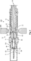
- a first embodiment of a connector 10 and a method for improving the impedance in the connector 10 is shown.
- the connector 10 can be used in the automotive field. However, other applications are of course also possible.
- the connector 10 is adapted to be connected to a mating connector 30 (see for example Fig. 2 ) by plugging the connector 10 along a plugging direction P into the mating connector 30.
- the connector 10 therefore has a contact element 11, which is in this example embodied as a pin that can be received in a mating contact element 31 of the mating connector 30, for example in a socket.
- the contact element 11 is arranged in an interior 15 of the connector 10 and is adapted to make contact to an electrical connection element 20 like the mating connector 30 at a distal end 13 or a cable 14 at a proximal end 14 opposite the distal end 13.
- the contact element 11 is attached to a core conductor 41 of the cable 40.
- the core conductor 41 is surrounded by a dielectric insulation 42 which is in turn surrounded by an outer conductor 43 of the cable 14.
- the conductor 10 further comprises an impedance improving element 50.
- the impedance improving element 50 is located at a side of the cable 40 in order to improve the connection between the cable 40 and the contact element 11.
- the impedance improving element 50 comprises a reception channel 51 for the contact element 11 in the connector 10, through which the contact element 11 extends. Further, the impedance improving element 50 comprises a deformation section 52 that is adapted to be deformed. In this case, the deformation section 52 is adapted to be deformed in a radial direction R that is perpendicular to the axial direction A along which the contact element 11 extends. The axial direction A is parallel to the plugging direction P.
- the deformation section 52 can comprise a foam material in order to be easily deformable.
- the deformation section can comprise a heat-shrinkable material.
- the deformation section 52 can be elastically or plastically deformable.
- the impedance improving element 50 is made from a dielectric material so that it provides an insulating effect.
- the impedance improving element 50 can, for example, be made from a plastic material or a rubber-like material.
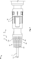
- the impedance improving element 50 is located at a proximal side 14 of the connector 10. It comprises a receptacle 54 for a dielectric insulation 42 of the cable 14. The dielectric insulation 42 thus protrudes into the interior 15 of the impedance improving element 50.
- the connector 10 comprises a crimping section 19 that is adapted to be crimped radially.
- the crimping section 19 is plastically deformable in the radial direction R.
- a crimping tool 200 is used to deform the crimping section 19 and the deformation section 52 of the impedance improving element 50 by applying a radial pressure.
- the crimping section 19 squeezes the impedance improving element 50 onto the cable 40 and thus also mechanically connects the two.
- the crimping process leaves an indent 191 in the housing 17 of the connector 10.
- the housing 17 also comprises a shielding 17 that is connected to the outer conductor 43 of the cable and provides an electromagnetic shielding.
- a cross-section is shown in which an indent 191 is located in the background.
- the deformation section 52 is located in a space 190 defined by the crimping section 19. After the crimping and the deformation, the interior of the impedance improving element 50 is sealed. The core conductor 41 of the cable is thus insulated from the outer conductor 43 and short circuits through conduction through air or dirt are minimized.
- the impedance improving element 50 can be mounted either to the cable 14 or to the connector 10 before the crimping takes place. This allows an easy assembly.
- the impedance improving element 50 can, for example, be attached by means of glue or through an elastic fit.
- the impedance improving element 50 When viewed from a front side, the impedance improving element 50 covers the entire circumference of the contact element. This maximizes the impedance improving effect and guarantees sealing.
- the amount to which the crimping tool 200 deforms the crimping section 19 and the deformation section 52 of the impedance improving element 50 can be adjusted depending on the desired impedance in this area. It can, for example, be adjusted during the crimping process by measuring the impedance. The impedance can, for example, be measured during the deformation process by TDR measurements.
- the crimping tool 200 can perform a crimping around the entire circumference of the connector 10 or only in parts.
- the adjustment can for example be done by adjusting the crimp height.
- the cross section 192 and/or the circumference of the housing 17 and the shielding 18 at the crimp section 19 can correspond to the cross section 430 and/or circumference at the outer conductor 43 of the cable 40. A deviation of plus/minus 20 % in these values can be considered as corresponding.
- the cross section 192 and/or the circumference at the crimp section 19 can be smaller than the cross section 430 and/or circumference at the outer conductor 430 of the cable 40. By this, nearby sections with bigger cross sections or circumferences can be compensated.
- the impedance at the deformation section 19 can be adjusted to correspond to the impedance of the cable 40.
- a deviation of plus/minus 20 % in the impedances can be considered as corresponding.
- the impedance at the deformation section 19 can be adjusted to be lower than the impedance of the cable. This can be used to compensate a higher impedance region before or after the crimping section 19.
- the impedance improving element 50 can be tube-like or sleeve like. This can enable an easy assembly. It can have a circular cross-section. In other embodiments, it can have different cross-sections.
- the impedance improving element 50 can have a first section 251 with a large inner diameter and a second section 252 with a smaller inner diameter.
- the contact element 11 can protrude out of the impedance improving element 50 through a through-hole 57 at a distal end 13. Simple contacting can be achieved with this.
- the contact element 11 and the through-hole 57 can have mating inclined surfaces 58, 118 to allow a precise positioning.
- the impedance improving element 50 can comprise a stop face 65 for corresponding elements of the mating connector. This can allow a precise positioning.
- the impedance improving element can comprise a sealing surface 59 at the distal side 13 for sealing the contact element 11 together with corresponding elements at the mating connector 30.
- a connection assembly 300 comprises the connector 10 and the cable 40 attached to the connector 10.
- a further embodiment of a connector 10 with an impedance improving element 50 is shown.
- the connector 10 is connected to the mating connector 30, which comprises a socket as a mating contact element 31 for the contact element 11 of the connector 10.
- the connector 10 is again used in the automotive field. In this field, large quantities of connectors 10 need to be manufactured at low cost. The manufactured connectors 10 then have big tolerances and the distance between the connector 10 and the counter connector 30 varies considerably. This leads to variations in the impedance of the connection assembly 300.
- the connector 10 further comprises a second impedance improving element 50 located around a front part of the contact element 11.
- This impedance improving element 50 again comprises a reception channel 51 for the contact element 11.
- This impedance improving element 50 also comprises a deformation section 52 adapted to be deformed.
- the deformation section 52 of this impedance improving element 50 can be deformed axially.
- the deformation section 52 is deformed along the axial direction A of the contact element 11.
- the embodiment shown in Figs. 6 and 7 comprises discs 170, the planes of which run along the radial direction R and are thus perpendicular to the plugging direction P and the axial direction A.
- the disks can thus provide an insulating effect.
- a further embodiment of a connector 10 is shown.
- the connector 10 again comprises the impedance improving element 50 located around the contact element 11.
- the impedance improving element 50 comprises a deformation section 52 that can be deformed axially.
- the deformation section 52 comprises a helicoid section 150 in which material is arranged in a screw-like manner.
- the axis 155 of the helicoid section 150 runs along the plugging direction P of the connector 10.
- Such a configuration can result in spring forces along the axial direction A.
- the deformation section 52 is automatically deformed. Thereby, the impedance is improved independent of the production tolerances.
- Fig. 8 shows a further embodiment of the connector 10.
- a deformation section 52 of the impedance improving element 50 comprises a zigzag section 160 with interconnected sections 151.
- Each of the interconnected sections 51 has a slight angle 152 relative to the radial direction R.
- the impedance improving element is located between an attachment section 16, at which the contact element 11 is attached to the housing 17 of the connector 10, and an end 111 of the contact element 11, the end 111 being configured to be connected to the electrical connection element 20 in the form of the mating connector 30.
- the impedance element 50 is located at the distal side 13 of the connector 10, the distal side 14 being configured to be connected to the mating connector 40.
- the impedance improving element 50 is located next to a contact area 81 in which the contact element 11 contacts the mating contact element 31.
- the impedance improving element 50 covers at least across its length 360° of the circumference of the contact element 10.
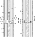
- Figs. 10A and 10B a further embodiment of a connector 10 with an impedance improving element 50 is shown.
- the connector 10 is connected to a mating connector 30 and shown with different mating depths in Figs. 10A and 10B .
- the impedance improving element 50 comprises a conductive material and is in a conductive electric connection with an outer conductor 63 of the connector 10.
- the outer conductor 63 is in this case a housing 17 which also serves as a shielding 18 and is connected to ground. This outer conductor 63 is also connected to an outer conductor 63 of the mating connector 30.
- the deformability of the impedance improving element 50 results in an improved impedance for all mating depths.
- the impedance improving element 50 is embodied as a ring that surrounds an empty space 64 which serves as the reception channel 51 for the contact element 11.
- Figs. 11A, 11B , 12A and 12B show further embodiments of a connector 10.
- the impedance improving element 50 and the deformation section 52 are radially deformable.
- the impedance improving element 50 is configured to contact an outer conductor 63 and comprises an electrically conductive material.
- the impedance improving element 50 is again located at a distal side 13 of the connector 10, the distal side 13 being the side that is adapted to contact the mating connector 30.
- the impedance improving element 50 has a basically torus-shaped configuration in which an outer ring has a hollow section 66 at the inside. Due to the hollow section 66, the deformability of the deformation section 52 is improved.
- a wedge-shaped front section 45 of the mating connector 30 deforms the impedance improving element 50 when it is connected to the counter connector.
- the impedance improving element 50 in particular the deformation section 52 is deformed radially and the hollow section 66 is squeezed to a minimal volume. Due to the fact that the deformation section 52 is deformed radially, the impedance of the impedance improvement element 50 differs depending on the mating or insertion depth of the mating connector 13, improving the overall impedance of the connection assembly 300.
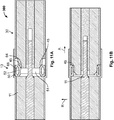
- a further embodiment is shown.
- the impedance improving element 50 is again located at a distal side 13 of the connector 10 and radially deformable.
- the deformation section 52 of the impedance improving element15 is deflected radially outwards due to a wedge-shaped front section 45 on the mating connector 30.
- a recess 68 is present in the connector 10.
- the recess 68 is formed by an outer conductor 63 of the connector 10.
- the recess 68 is channel-like with the channel being open radially inwards in order to take up the radially outwardly deflecting impedance improving element.
- This impedance improving element 50 can again be electrically conductive and in electric contact with the outer conductor 63 of the connector 10.
- the deflection of the impedance improving element 50, in particular the deformation section 52 varies. Accordingly, the appearance in this area also varies and the overall impedance of the connection assembly 300 is improved relative to a configuration without an impedance improving element 50.
- the impedance improving elements 50 are separate parts that can be manufactured separately. In other embodiments, however, the impedance improving elements 50 could be integrated into or be monolithic with other parts. For example, a housing 17 or a dielectric insulation between a core conductor and an outer conductor could form an impedance improving element 50.
Abstract
The application shows a connector (10) for high-frequency transmissions in the automotive field, comprising a contact element (11) arranged in an interior (15) of the connector (10) and adapted to make contact to an electrical connection element (20) like a cable (40) or a mating connector (30), the connector (10) further comprising an impedance improving element 50 located at a side of the electrical connection element (20), wherein the impedance improving element (50) comprises a reception channel (51) through which the contact element (11) extends and a deformation section (52) adapted to be deformed, at least one of radially or axially. Further, a connection assembly (300) comprising a connector (10) and a cable (40) attached to the connector (10), wherein the deformation section (52) seals and/or holds a dielectric insulation (42) of the cable (14), is disclosed. Moreover, shown is a method of improving the impedance in a connector (10) with a contact element (11), wherein an impedance improving element (50) is used, the impedance improving element (50) comprising a reception channel (51) for the contact element (11) and a deformation section (52) adapted to be deformed.
Description
- The invention relates to a connector for high-frequency transmissions in the automotive field, an impedance improving element, a connection assembly, and a method of improving the impedance in a connector.
- Connectors that are used in the automotive field are produced in large quantities. It has recently become desirable to transmit data with a high rate and thus at high frequencies. However, current connectors suitable for high-frequency transmissions are difficult to produce and expensive and thus unsuitable for the automotive field.
- It is the object of the invention to provide a solution that allows producing large quantities of connectors that are suitable for high-frequency transmissions, in particular in the automotive field.
- According to the invention, this is achieved by a connector for high-frequency transmissions in the automotive field, comprising at least one contact element arranged in an interior of the connector and adapted to make contact to an electrical connection element like a cable or a mating connector, the connector further comprising an impedance improving element located at a side of the electrical connection element, wherein the impedance improving element comprises a reception channel through which the at least one contact element extends, and a deformation section adapted to be deformed, at least one of radially or axially.
- An impedance improving element according to the invention is adapted to be used in a connector according to the invention.
- A connection assembly according to the invention comprises a connector according to the invention.
- The object is further achieved by a method of improving the impedance in a connector with a contact element, wherein an impedance improving element is used, the element comprising a reception channel for the contact element and a deformation section adapted to be deformed.
- The solution according to the invention can further be improved by the following further developments and advantageous embodiments, which are independent of each other and can be combined arbitrarily, as desired.
- The impedance improving element may be located between an attachment section, at which the contact element is attached to a housing of the connector, and an end of the at least one contact element, the end being configured to be connected to the electrical connection element. The impedance improving effect is hereby optimized.
- For example, the impedance improving element can be located between the cable and the attachment section or located between the mating connector and the attachment section.
- In a simple configuration, the deformation section can comprise a foam material. Such a material can be easily deformable. The foam material can be an open or closed cell foam material.
- Advantageously, the impedance improving element can be made from a dielectric material. The material can for example comprise plastic. This allows an easy production.
- In a further development, the impedance improving element can comprise a conductive material. In particular, the impedance improving element can consist of a conductive material. The conductive material can for example be a metal or a material comprising metal, for instance a hybrid material comprising a dielectric material and a conductive network within the dielectric material.
- The deformation section can be elastically deformable to allow repeated use of the impedance improving element.
- In an alternative, the deformation section can be plastically deformable. This can allow a stable configuration.
- In an advantageous development, the deformation section can comprise a heat-shrinkable material. This can improve the manufacturing process, as such a material can be applied in an un-shrunken state and then be shrunk by applying heat.
- In a first advantageous development, the impedance improving element is located at a proximal side of the connector, the proximal side being configured to be connected to the cable, and comprises a receptacle for a dielectric insulation of a cable, wherein the deformation section is adapted to be deformed radially. In such a development, the impedance in the transition between the cable and the connector can be improved.
- The connector can comprise a crimping section and the impedance improving element can be located at the crimping section. For example, the impedance improving element can be located in a space defined by the crimping section, if the crimping section is closed around a circumferential direction, for example if it is cylindrical.
- The crimping section can be, at least in sections, plastically deformable in the radial direction. The crimping section can for example comprise a metal that is deformable by a crimping tool. The amount to which the crimping section is deformed can be controlled and adjusted to a desired impedance.
- The impedance improving element can be mounted to a shielding element of the connector. The electrical connection element can then be inserted into the connector easily so that the manufacturing is simplified.
- The impedance improving element can for example be mounted to the shielding element with glue or through an elastic fit.
- The shielding element can be a part of the housing. In particular, the shielding element can make up the entire housing of the connector.ln a further advantageous development, the impedance improving element is located at a distal side of the connector, the distal side being configured to be connected to the mating connector, and the deformation section is adapted to be deformed axially by a mating connector. In such a development, the impedance in the transition area between the connector and the mating connector can be improved.
- In order to compensate for tolerances during the production process that lead to different distances between the connector and the mating connector in the assembled state, the deformation section can comprise a spring section that is elastically deformable in a plugging direction. The plugging direction is the direction along which the connector is mated with the mating connector.
- In one alternative, the deformation section can comprise a helicoid section. Such a configuration can have a spring function. The spring constant can be, for example, adjusted by an appropriate choice of material thickness and winding density of the helicoid section.
- The axis of the helicoid can be parallel to the plugging direction of the connector in order to allow a simple operation.
- In a further alternative, the deformation section can comprise a meander section. This can allow for application of material for improving the impedance while maintaining a degree of deformability.
- In a further alternative, the deformation section can comprise disks. The disks can have an insulating effect.
- The deformation section can comprise a zigzag section. The zigzag section can have several interconnected sections at angles to each other. Each of the interconnected sections can be slightly angled to a direction perpendicular to the plugging direction. Such a configuration can have a spring effect while providing material for improving the impedance in the areas around the contact element.
- The impedance improving element can be produced by a moulding process. The impedance improving element can be moulded onto an existing element, for example the housing. Alternatively, the impedance improving element can be a separate part that can be attached to a further part. The impedance improving element can be configured to be attached to already existing connectors to improve their performance.
- In an alternative embodiment, the impedance improving element can be produced by machining.
- The impedance improving element can comprise visco-elastic materials such as dry silicone gel. These materials can be squeezed into non-functional voids which has the additional advantage of a constant permittivity.
- In a further advantageous development, the impedance improving element is located at a distal side of the connector, the distal side being configured to be connected to the mating connector, wherein the deformation section is adapted to be deformed radially. In such a development, the impedance in the transition between the cable and the connector can be improved.
- The impedance improving element can be configured to contact an outer conductor of the connector or the electrical connection element, in particular the mating connector or the cable. In a mounted state, the impedance improving element can contact the outer conductor. The outer conductor can be a part of a shielding or a housing of the connector. The outer conductor can be connected to ground or a similar common voltage level.
- The connector can comprise a recess configured to take up the impedance improving element, in particular in a deformed state. For example, the recess can comprise a channel and be adapted to take up parts of the deformation section of the impedance improving element, for instance when it is deformed. In particular, the recess can be open radially inwards in order to take up an impedance improving element that is deformable radially outwards.
- The impedance improving element and the deformation section can comprise a hollow section in order to allow an easy deformation with a low force.A connection assembly can comprise a connector according to the invention and a cable attached to the connector, wherein the deformation section seals and/or holds a dielectric insulation of the cable. Air and creeping connections along which an electrical shortcut can occur can thus be avoided or elongated.
- In order to keep the manufacturing simple, the impedance improving element can be mounted to a dielectric insulation of the cable before the connection between the cable and the connector is made. The connector can then be slid over such an arrangement.
- A connection assembly can comprise a connector according to the invention and a mating connector with at least one mating contact element for the contact element, wherein the impedance improving element surrounds a contact area in which the at least one contact element and the at least one mating contact element contact each other. With such an embodiment, the impedance in the transition between the at least contact element and the at least one mating contact element can be improved.
- In order to achieve a good impedance improving, the impedance improving element can cover at least across its length 360° of the circumference of the at least one contact element.
- A method according to the invention can advantageously comprise the step of deforming the deformation section.
- For example, the deformation section can be at least partially moved over a dielectric insulation of a cable and the deformation section can be subsequently deformed radially.
- In order to adjust the impedance, the deformation can be controlled depending on the impedance of the connector and/or the connection assembly. The impedance can, for example, be measured during the deformation process by TDR measurements.
- The adjustment can for example be done by adjusting the crimp height. For example, the cross section and/or the circumference of the crimp section can correspond to the cross section and/or circumference of the outer conductor of the cable. A deviation of plus/minus 20 % in these values can be considered as corresponding.
- The cross section and/or the circumference at the crimp section can be smaller than the cross section and/or circumference at the outer conductor of the cable. By this, nearby sections with bigger cross sections or circumferences can be compensated.
- The impedance between the core conductor and outer conductor at the deformation section can be adjusted to correspond to the impedance of the cable. A deviation of plus/minus 20 % in the impedances can be considered as corresponding.
- The impedance at the deformation section can be adjusted to be lower than the impedance of the cable. This can be used to compensate a higher impedance region before or after the crimping section.
- In an advantageous embodiment, the deformation section or the impedance improving element can be deformed radially and the impedance improving element can be adapted to contact an outer conductor of the connector or the electrical connection element.
- In a further embodiment, the deformation section can be deformed axially. This may be due to the movement of a mating connector during a connection step. In particular, the deforming can occur automatically during the plugging process. The impedance improving element can comprise stop faces at a front for mating faces of the mating connector to achieve such an automatic deformation.
- The impedance improving element can be tube-like or sleeve like. This can enable an easy assembly. For example, the impedance improving element can at least in sections have a circular cross-section in order to improve the mounting process. Alternatively, it can have other types of cross-sections, for example a rectangular or an elliptic cross-section.
- The impedance improving element can have a first section with a large inner diameter and a second section with a smaller inner diameter. The first section may face towards a proximal side. The second section may face towards a distal side.
- The at least one contact element can protrude out of the impedance improving element through a through-hole at a front section. Simple contacting can be achieved with this.
- The at least one contact element and the through-hole can have mating inclined or beveled surfaces to allow a precise positioning and a sealing effect.
- The impedance improving element can comprise a stop face for corresponding elements of the mating connector. This can allow a precise positioning.
- The impedance improving element can comprise a sealing surface at a front for sealing the at least one contact element together with corresponding elements at the mating connector.
- In order to allow for example the use of different materials, the impedance improving element can be a separate part. It can be a part that can be produced separately and be added later to existing connectors to improve their impedance performance.
- In a further embodiment, the impedance improving element can be integrated into and/or monolithic with other elements. For example, the impedance improving element can be integrated into or be formed by an insulation part, in particular a dielectric insulation between a core conductor and an outer conductor.
- The invention will now be described in greater detail and in an exemplary manner using advantageous embodiments and with reference to the drawings. The described embodiments are only possible configurations in which, however, the individual features as described above can be provided independently of one another or can be omitted.
- In the figures:
- Fig. 1
- shows a schematic longitudinal cross-section through an embodiment of a connector;
- Fig. 2
- shows a schematic longitudinal cross-section through the embodiment of
Fig. 1 during a method step; - Fig. 3
- shows an enlarged view of a detail of
Fig. 2 ; - Fig. 4
- shows a schematic longitudinal cross-section through the embodiment of
Fig. 1 after a crimping step; - Fig. 5
- shows an enlarged view of a detail of
Fig. 4 ; - Fig. 6
- shows a schematic longitudinal cross-section through the further embodiment of a connector;
- Fig. 7
- shows a schematic side view of the embodiment of a connector shown in
Fig. 6 ; - Fig. 8
- shows a schematic side view of a further embodiment of a connector;
- Fig. 9
- shows a schematic side view of a further embodiment of a connector;
- Figs. 10A and 10B
- show schematic cross-sections through a further embodiment of a connector in a first state and a second state;
- Figs. 11A and 11B
- show schematic cross-sections through a further embodiment of a connector in a first state and a second state; and
- Figs. 12A and 12B
- show schematic cross-sections through a further embodiment of a connector in a first state and a second state.
- In
Figs. 1 to 5 , a first embodiment of aconnector 10 and a method for improving the impedance in theconnector 10 is shown. - The
connector 10 can be used in the automotive field. However, other applications are of course also possible. - The
connector 10 is adapted to be connected to a mating connector 30 (see for exampleFig. 2 ) by plugging theconnector 10 along a plugging direction P into themating connector 30. Theconnector 10 therefore has acontact element 11, which is in this example embodied as a pin that can be received in amating contact element 31 of themating connector 30, for example in a socket. Thecontact element 11 is arranged in an interior 15 of theconnector 10 and is adapted to make contact to anelectrical connection element 20 like themating connector 30 at adistal end 13 or acable 14 at aproximal end 14 opposite thedistal end 13. - In particular, the
contact element 11 is attached to acore conductor 41 of thecable 40. Thecore conductor 41 is surrounded by adielectric insulation 42 which is in turn surrounded by anouter conductor 43 of thecable 14. - The
conductor 10 further comprises animpedance improving element 50. In this case, theimpedance improving element 50 is located at a side of thecable 40 in order to improve the connection between thecable 40 and thecontact element 11. - The
impedance improving element 50 comprises areception channel 51 for thecontact element 11 in theconnector 10, through which thecontact element 11 extends. Further, theimpedance improving element 50 comprises adeformation section 52 that is adapted to be deformed. In this case, thedeformation section 52 is adapted to be deformed in a radial direction R that is perpendicular to the axial direction A along which thecontact element 11 extends. The axial direction A is parallel to the plugging direction P. - The
deformation section 52 can comprise a foam material in order to be easily deformable. In other embodiments, the deformation section can comprise a heat-shrinkable material. - The
deformation section 52 can be elastically or plastically deformable. - The
impedance improving element 50 is made from a dielectric material so that it provides an insulating effect. Theimpedance improving element 50 can, for example, be made from a plastic material or a rubber-like material. - The
impedance improving element 50 is located at aproximal side 14 of theconnector 10. It comprises areceptacle 54 for adielectric insulation 42 of thecable 14. Thedielectric insulation 42 thus protrudes into the interior 15 of theimpedance improving element 50. - The
connector 10 comprises a crimpingsection 19 that is adapted to be crimped radially. The crimpingsection 19 is plastically deformable in the radial direction R. As shown inFigs. 2 to 5 , a crimpingtool 200 is used to deform the crimpingsection 19 and thedeformation section 52 of theimpedance improving element 50 by applying a radial pressure. In this crimping step, the crimpingsection 19 squeezes theimpedance improving element 50 onto thecable 40 and thus also mechanically connects the two. The crimping process leaves anindent 191 in thehousing 17 of theconnector 10. Thehousing 17 also comprises a shielding 17 that is connected to theouter conductor 43 of the cable and provides an electromagnetic shielding. InFig. 2 , a cross-section is shown in which anindent 191 is located in the background. - The
deformation section 52 is located in aspace 190 defined by the crimpingsection 19. After the crimping and the deformation, the interior of theimpedance improving element 50 is sealed. Thecore conductor 41 of the cable is thus insulated from theouter conductor 43 and short circuits through conduction through air or dirt are minimized. - The
impedance improving element 50 can be mounted either to thecable 14 or to theconnector 10 before the crimping takes place. This allows an easy assembly. Theimpedance improving element 50 can, for example, be attached by means of glue or through an elastic fit. - When viewed from a front side, the
impedance improving element 50 covers the entire circumference of the contact element. This maximizes the impedance improving effect and guarantees sealing. - The amount to which the crimping
tool 200 deforms the crimpingsection 19 and thedeformation section 52 of theimpedance improving element 50 can be adjusted depending on the desired impedance in this area. It can, for example, be adjusted during the crimping process by measuring the impedance. The impedance can, for example, be measured during the deformation process by TDR measurements. - The crimping
tool 200 can perform a crimping around the entire circumference of theconnector 10 or only in parts. - The adjustment can for example be done by adjusting the crimp height. For example, the
cross section 192 and/or the circumference of thehousing 17 and the shielding 18 at thecrimp section 19 can correspond to the cross section 430 and/or circumference at theouter conductor 43 of thecable 40. A deviation of plus/minus 20 % in these values can be considered as corresponding. - The
cross section 192 and/or the circumference at thecrimp section 19 can be smaller than the cross section 430 and/or circumference at the outer conductor 430 of thecable 40. By this, nearby sections with bigger cross sections or circumferences can be compensated. - The impedance at the
deformation section 19 can be adjusted to correspond to the impedance of thecable 40. A deviation of plus/minus 20 % in the impedances can be considered as corresponding. - The impedance at the
deformation section 19 can be adjusted to be lower than the impedance of the cable. This can be used to compensate a higher impedance region before or after the crimpingsection 19. - The
impedance improving element 50 can be tube-like or sleeve like. This can enable an easy assembly. It can have a circular cross-section. In other embodiments, it can have different cross-sections. - The
impedance improving element 50 can have a first section 251 with a large inner diameter and a second section 252 with a smaller inner diameter. - The
contact element 11 can protrude out of theimpedance improving element 50 through a through-hole 57 at adistal end 13. Simple contacting can be achieved with this. - The
contact element 11 and the through-hole 57 can have mating inclined surfaces 58, 118 to allow a precise positioning. - The
impedance improving element 50 can comprise astop face 65 for corresponding elements of the mating connector. This can allow a precise positioning. - The impedance improving element can comprise a sealing
surface 59 at thedistal side 13 for sealing thecontact element 11 together with corresponding elements at themating connector 30. - A
connection assembly 300 comprises theconnector 10 and thecable 40 attached to theconnector 10. - In
Figs. 6 and7 , a further embodiment of aconnector 10 with animpedance improving element 50 is shown. InFig. 6 , theconnector 10 is connected to themating connector 30, which comprises a socket as amating contact element 31 for thecontact element 11 of theconnector 10. - The
connector 10 is again used in the automotive field. In this field, large quantities ofconnectors 10 need to be manufactured at low cost. The manufacturedconnectors 10 then have big tolerances and the distance between theconnector 10 and thecounter connector 30 varies considerably. This leads to variations in the impedance of theconnection assembly 300. - Apart from the already described
impedance improving element 50 located in the transition area between thecontact element 11 and thecable 40, theconnector 10 further comprises a secondimpedance improving element 50 located around a front part of thecontact element 11. Thisimpedance improving element 50 again comprises areception channel 51 for thecontact element 11. Thisimpedance improving element 50 also comprises adeformation section 52 adapted to be deformed. Thedeformation section 52 of thisimpedance improving element 50 can be deformed axially. When making contact to themating connector 30, thedeformation section 52 is deformed along the axial direction A of thecontact element 11. By this, the space between thecontact element 11 and ahousing 17 of theconnector 10 is filled with dielectric material and the impedance is improved. - The embodiment shown in
Figs. 6 and7 comprisesdiscs 170, the planes of which run along the radial direction R and are thus perpendicular to the plugging direction P and the axial direction A. The disks can thus provide an insulating effect. - In
Fig. 8 , a further embodiment of aconnector 10 is shown. Theconnector 10 again comprises theimpedance improving element 50 located around thecontact element 11. Theimpedance improving element 50 comprises adeformation section 52 that can be deformed axially. Thedeformation section 52 comprises ahelicoid section 150 in which material is arranged in a screw-like manner. Theaxis 155 of thehelicoid section 150 runs along the plugging direction P of theconnector 10. - Such a configuration can result in spring forces along the axial direction A. When the
connector 10 is plugged into themating connector 30, thedeformation section 52 is automatically deformed. Thereby, the impedance is improved independent of the production tolerances. -
Fig. 8 shows a further embodiment of theconnector 10. In this embodiment, adeformation section 52 of theimpedance improving element 50 comprises azigzag section 160 withinterconnected sections 151. Each of theinterconnected sections 51 has aslight angle 152 relative to the radial direction R. - In the embodiments of
Figs. 6 to 9 , the impedance improving element is located between anattachment section 16, at which thecontact element 11 is attached to thehousing 17 of theconnector 10, and anend 111 of thecontact element 11, theend 111 being configured to be connected to theelectrical connection element 20 in the form of themating connector 30. - Further, in the embodiments of
Figs. 6 to 9 , theimpedance element 50 is located at thedistal side 13 of theconnector 10, thedistal side 14 being configured to be connected to themating connector 40. - The
impedance improving element 50 is located next to acontact area 81 in which thecontact element 11 contacts themating contact element 31. - Moreover, the
impedance improving element 50 covers at least across its length 360° of the circumference of the contact element 10.InFigs. 10A and 10B , a further embodiment of aconnector 10 with animpedance improving element 50 is shown. Theconnector 10 is connected to amating connector 30 and shown with different mating depths inFigs. 10A and 10B . - The
impedance improving element 50 comprises a conductive material and is in a conductive electric connection with anouter conductor 63 of theconnector 10. Theouter conductor 63 is in this case ahousing 17 which also serves as a shielding 18 and is connected to ground. Thisouter conductor 63 is also connected to anouter conductor 63 of themating connector 30. - The deformability of the
impedance improving element 50 results in an improved impedance for all mating depths. - The
impedance improving element 50 is embodied as a ring that surrounds anempty space 64 which serves as thereception channel 51 for thecontact element 11. -
Figs. 11A, 11B ,12A and 12B show further embodiments of aconnector 10. In these embodiments, theimpedance improving element 50 and thedeformation section 52 are radially deformable. As in the embodiment ofFigs. 10A and 10B , theimpedance improving element 50 is configured to contact anouter conductor 63 and comprises an electrically conductive material. - The
impedance improving element 50 is again located at adistal side 13 of theconnector 10, thedistal side 13 being the side that is adapted to contact themating connector 30. Theimpedance improving element 50 has a basically torus-shaped configuration in which an outer ring has ahollow section 66 at the inside. Due to thehollow section 66, the deformability of thedeformation section 52 is improved. A wedge-shapedfront section 45 of themating connector 30 deforms theimpedance improving element 50 when it is connected to the counter connector. During this insertion process, theimpedance improving element 50, in particular thedeformation section 52 is deformed radially and thehollow section 66 is squeezed to a minimal volume. Due to the fact that thedeformation section 52 is deformed radially, the impedance of theimpedance improvement element 50 differs depending on the mating or insertion depth of themating connector 13, improving the overall impedance of theconnection assembly 300. - In
Figs. 12A and 12B , a further embodiment is shown. Theimpedance improving element 50 is again located at adistal side 13 of theconnector 10 and radially deformable. When themating connector 30 is inserted into aconnector 10, thedeformation section 52 of the impedance improving element15 is deflected radially outwards due to a wedge-shapedfront section 45 on themating connector 30. To take up theimpedance improving element 50, arecess 68 is present in theconnector 10. Therecess 68 is formed by anouter conductor 63 of theconnector 10. Therecess 68 is channel-like with the channel being open radially inwards in order to take up the radially outwardly deflecting impedance improving element. - This
impedance improving element 50 can again be electrically conductive and in electric contact with theouter conductor 63 of theconnector 10. Depending on the insertion depth of themating connector 13, the deflection of theimpedance improving element 50, in particular thedeformation section 52 varies. Accordingly, the appearance in this area also varies and the overall impedance of theconnection assembly 300 is improved relative to a configuration without animpedance improving element 50. - In the depicted embodiments, the
impedance improving elements 50 are separate parts that can be manufactured separately. In other embodiments, however, theimpedance improving elements 50 could be integrated into or be monolithic with other parts. For example, ahousing 17 or a dielectric insulation between a core conductor and an outer conductor could form animpedance improving element 50. -
- 10
- connector
- 11
- contact element
- 12
- side of electrical connection element
- 13
- distal side
- 14
- proximal side
- 15
- interior
- 16
- attachment section
- 17
- housing
- 18
- shielding
- 19
- crimping section
- 20
- electrical connection element
- 30
- mating connector
- 31
- mating contact element
- 40
- cable
- 41
- core conductor
- 42
- insulation
- 43
- outer conductor
- 45
- front section
- 50
- impedance improving element
- 51
- reception channel
- 52
- deformation section
- 54
- receptacle
- 55
- spring section
- 57
- through-hole
- 58
- inclined surface
- 59
- sealing surface
- 63
- outer conductor
- 64
- empty space
- 65
- stop face
- 66
- hollow section
- 68
- recess
- 81
- contact area
- 111
- end of contact element
- 118
- inclined surface
- 150
- helicoid section
- 151
- interconnected section
- 152
- angle
- 155
- axis
- 160
- zigzag section
- 170
- disk
- 190
- space defined by crimping section
- 191
- indent
- 192
- cross-section
- 200
- crimping tool
- 251
- first section
- 252
- second section
- 300
- connection assembly
- 430
- cross-section
- A
- axial direction
- P
- plugging direction
- R
- radial direction
Claims (15)
- Connector (10) for high-frequency transmissions in the automotive field, comprising at least one contact element (11) arranged in an interior (15) of the connector (10) and adapted to make contact to an electrical connection element (20) like a cable (40) or a mating connector (30), the connector (10) further comprising an impedance improving element (50) located at a side of the electrical connection element (20), wherein the impedance improving element (50) comprises a reception channel (51) through which the at least one contact element (11) extends and a deformation section (52) adapted to be deformed, at least one of radially or axially.
- Connector (10) according to claim 1, wherein the impedance improving element (50) is located at a proximal side (14) of the connector (10), the proximal side (14) being configured to be connected to the cable (40), and comprises a receptacle (54) for a dielectric insulation (42) of the cable (40) and wherein the deformation section (52) is adapted to be deformed radially.
- Connector (10) according to claim 1 or 2, wherein the connector (10) comprises a crimping section (19) and the impedance improving element (50) is located at the crimping section (19).
- Connector (10) according to one of claims 1 to 3, wherein the impedance improving element (50) is mounted to a shielding (18) of the connector (10).
- Connector (10) according to one of claims 1 to 4, wherein the impedance improving element (50) is located at a distal side (13) of the connector (10), the distal side (13) being configured to be connected to the mating connector (30), and the deformation section (52) is adapted to be deformed axially by the mating connector (30).
- Connector (10) according to one of claims 1 to 5, wherein the impedance improving element (50) is located at a distal side (13) of the connector (10), the distal side (13) being configured to be connected to the mating connector (30), and the deformation section (52) is adapted to be deformed radially by the mating connector (30).
- Connector (10) according to one of claims 1 to 6, wherein the impedance improving element (50) is located between an attachment section (16), at which the at least one contact element (11) is attached to a housing (17) of the connector (10), and an end (111) of the at least one contact element (11), the end (111) being configured to be connected to the electrical connection element (20).
- Connector (10) according to one of claims 1 to 7, wherein the deformation section (52) comprises a foam material.
- Impedance improving element (50) adapted to be used in a connector (10) according to one of claims 1 to 8.
- Connection assembly (300) comprising a connector (10) according to one of claims 1 to 8 and a cable (40) attached to the connector (10), wherein the deformation section (52) seals and/or holds a dielectric insulation (42) of the cable (14).
- Connection assembly (300) according to claim 10, wherein the impedance improving element (50) is mounted to a dielectric insulation (42) of the cable (40).
- Method of improving the impedance in a connector (10) with at least one contact element (11), wherein an impedance improving element (50) is used, the impedance improving element (50) comprising a reception channel (51) for the at least one contact element (11) and a deformation section (52) adapted to be deformed.
- Method according to claim 12, wherein the method comprises the step of deforming the deformation section (52).
- Method according to claim 12 or 13, wherein the deformation section (52) is at least partially moved over a dielectric insulation (42) of a cable (40) and the deformation section (52) is subsequently deformed radially.
- Method according to one of claims 12 to 14, wherein the deformation is controlled depending on the impedance of the connector (10).
Priority Applications (6)
| Application Number | Priority Date | Filing Date | Title |
|---|---|---|---|
| EP19169265.6A EP3726667A1 (en) | 2019-04-15 | 2019-04-15 | Connector for high-frequency transmissions in the automotive field, impedance improving element, connection assembly, method of improving the impedance in a connector |
| JP2020070689A JP2020177909A (en) | 2019-04-15 | 2020-04-10 | Connector for high-frequency transmission in automotive field, impedance improving element, connection assembly, and method of improving impedance in connector |
| KR1020200044420A KR20200121242A (en) | 2019-04-15 | 2020-04-13 | Connector for high-frequency transmissions in the automotive field, impedance improving element, connection assembly, method of improving the impedance in a connector |
| CN202010288974.XA CN111834774A (en) | 2019-04-15 | 2020-04-14 | Connector, impedance improving member, connecting assembly, and method of improving impedance of connector |
| EP20169299.3A EP3726668A1 (en) | 2019-04-15 | 2020-04-14 | Connector for high-frequency transmissions in the automotive field, impedance improving element, connection assembly, method of improving the impedance in a connector |
| US16/849,627 US11233360B2 (en) | 2019-04-15 | 2020-04-15 | Connector for high-frequency transmissions in the automotive field, impedance improving element, connection assembly, method of improving the impedance in a connector |
Applications Claiming Priority (1)
| Application Number | Priority Date | Filing Date | Title |
|---|---|---|---|
| EP19169265.6A EP3726667A1 (en) | 2019-04-15 | 2019-04-15 | Connector for high-frequency transmissions in the automotive field, impedance improving element, connection assembly, method of improving the impedance in a connector |
Publications (1)
| Publication Number | Publication Date |
|---|---|
| EP3726667A1 true EP3726667A1 (en) | 2020-10-21 |
Family
ID=66182431
Family Applications (2)
| Application Number | Title | Priority Date | Filing Date |
|---|---|---|---|
| EP19169265.6A Withdrawn EP3726667A1 (en) | 2019-04-15 | 2019-04-15 | Connector for high-frequency transmissions in the automotive field, impedance improving element, connection assembly, method of improving the impedance in a connector |
| EP20169299.3A Pending EP3726668A1 (en) | 2019-04-15 | 2020-04-14 | Connector for high-frequency transmissions in the automotive field, impedance improving element, connection assembly, method of improving the impedance in a connector |
Family Applications After (1)
| Application Number | Title | Priority Date | Filing Date |
|---|---|---|---|
| EP20169299.3A Pending EP3726668A1 (en) | 2019-04-15 | 2020-04-14 | Connector for high-frequency transmissions in the automotive field, impedance improving element, connection assembly, method of improving the impedance in a connector |
Country Status (5)
| Country | Link |
|---|---|
| US (1) | US11233360B2 (en) |
| EP (2) | EP3726667A1 (en) |
| JP (1) | JP2020177909A (en) |
| KR (1) | KR20200121242A (en) |
| CN (1) | CN111834774A (en) |
Cited By (2)
| Publication number | Priority date | Publication date | Assignee | Title |
|---|---|---|---|---|
| DE102020106243A1 (en) | 2020-03-09 | 2021-09-09 | Md Elektronik Gmbh | Connector arrangement for electrically connecting two cables |
| US11916346B2 (en) | 2020-07-24 | 2024-02-27 | Te Connectivity Germany Gmbh | Method of crimping an electrical HF connection device |
Families Citing this family (1)
| Publication number | Priority date | Publication date | Assignee | Title |
|---|---|---|---|---|
| DE102021112505A1 (en) * | 2021-05-12 | 2022-11-17 | Te Connectivity Germany Gmbh | Crimp contact, crimp connection and method of making a crimp connection |
Citations (5)
| Publication number | Priority date | Publication date | Assignee | Title |
|---|---|---|---|---|
| US3711942A (en) * | 1968-01-04 | 1973-01-23 | Amp Inc | Coaxial connector controlled characteristic impedance process |
| US20060030208A1 (en) * | 2004-08-05 | 2006-02-09 | Cassanego Paul E | Microwave connector |
| US20100297867A1 (en) * | 2007-06-25 | 2010-11-25 | Rosenberger Hochfrequenztechnik Gmbh & Co. Kg | Co-axial connector |
| JP2011124136A (en) * | 2009-12-11 | 2011-06-23 | Autonetworks Technologies Ltd | Shield connector |
| JP2019029103A (en) * | 2017-07-26 | 2019-02-21 | 第一精工株式会社 | Coaxial connector and evaluation jig |
Family Cites Families (47)
| Publication number | Priority date | Publication date | Assignee | Title |
|---|---|---|---|---|
| US2904619A (en) | 1954-07-23 | 1959-09-15 | Amp Inc | Shielded wire connectors |
| US3384703A (en) | 1964-05-26 | 1968-05-21 | Amp Inc | Coaxial connector |
| US3283287A (en) | 1964-11-24 | 1966-11-01 | Amp Inc | Connector ferrule with improved seal construction |
| US3439294A (en) | 1965-05-28 | 1969-04-15 | Amphenol Corp | Coaxial cable connector |
| US3373243A (en) | 1966-06-06 | 1968-03-12 | Bendix Corp | Electrical multiconductor cable connecting assembly |
| US3868616A (en) | 1967-08-15 | 1975-02-25 | Edward H Yonkers | Grounded surface distribution apparatus |
| US3499101A (en) | 1968-08-23 | 1970-03-03 | Amp Inc | Outer conductor crimp for coaxial devices |
| US3681739A (en) | 1970-01-12 | 1972-08-01 | Reynolds Ind Inc | Sealed coaxial cable connector |
| US3824686A (en) | 1972-05-12 | 1974-07-23 | Amp Inc | A method of terminating a semi-rigid coaxial cable |
| US3797104A (en) | 1972-07-13 | 1974-03-19 | W Pote | Flexible coaxial cable and method of making same |
| US4426127A (en) | 1981-11-23 | 1984-01-17 | Omni Spectra, Inc. | Coaxial connector assembly |
| GB8518141D0 (en) | 1985-07-18 | 1985-08-21 | Raychem Ltd | Electrical crimp connection |
| EP0339067B1 (en) | 1987-10-15 | 1996-07-31 | Palco Connector Inc. | Constant impedance high frequency coaxial connector |
| US4789351A (en) | 1988-04-29 | 1988-12-06 | Amp Incorporated | Blind mating connector with snap ring insertion |
| US5083943A (en) | 1989-11-16 | 1992-01-28 | Amphenol Corporation | Catv environmental f-connector |
| US5123864A (en) | 1991-04-05 | 1992-06-23 | Amp Incorporated | Coaxial contact with sleeve |
| US5217391A (en) | 1992-06-29 | 1993-06-08 | Amp Incorporated | Matable coaxial connector assembly having impedance compensation |
| GB2271678B (en) | 1993-12-03 | 1994-10-12 | Itt Ind Ltd | Electrical connector |
| DE19632905A1 (en) | 1996-08-16 | 1998-02-19 | Itt Cannon Gmbh | Electrical connector |
| JPH11195448A (en) | 1997-12-26 | 1999-07-21 | Amp Japan Ltd | Waterproof-type electric connector |
| JP3767783B2 (en) | 1999-08-30 | 2006-04-19 | 矢崎総業株式会社 | Half-mating prevention connector |
| US6666698B2 (en) | 2000-08-17 | 2003-12-23 | Tyco Electronics Corporation | Arc limiting electrical connector assembly |
| US6641421B1 (en) | 2002-09-09 | 2003-11-04 | Reynolds Industries, Inc. | High-voltage electrical connector and related method |
| US6869320B2 (en) | 2003-04-23 | 2005-03-22 | Hewlett-Packard Development Company, L.P. | Portable modular electronic system with symmetrical connections |
| US8142223B2 (en) | 2004-08-27 | 2012-03-27 | Belden Inc. | Universal cable connector with interchangeable color bands |
| US7351101B1 (en) | 2006-08-17 | 2008-04-01 | John Mezzalingua Associates, Inc. | Compact compression connector for annular corrugated coaxial cable |
| JP5332677B2 (en) | 2009-02-09 | 2013-11-06 | 株式会社オートネットワーク技術研究所 | Cable connector and cable with cable connector |
| DE102009019626B3 (en) * | 2009-04-30 | 2011-03-03 | Tyco Electronics Amp Gmbh | Electrical connector with impedance correcting element and method of making the same |
| US9159472B2 (en) | 2010-12-08 | 2015-10-13 | Pandult Corp. | Twinax cable design for improved electrical performance |
| US8366483B2 (en) | 2011-02-04 | 2013-02-05 | Tyco Electronics Corporation | Radio frequency connector assembly |
| US8333603B1 (en) | 2011-05-23 | 2012-12-18 | Delphi Technologies, Inc. | Electrical connection system having dielectric spring to absorb axial positional mating tolerance variation for multiple connectors |
| USRE46958E1 (en) | 2011-10-24 | 2018-07-17 | Ardent Concepts, Inc. | Controlled-impedance cable termination using compliant interconnect elements |
| US8727807B2 (en) | 2011-10-28 | 2014-05-20 | Tyco Electronics Corporation | Coaxial connector |
| US8574007B2 (en) | 2012-04-06 | 2013-11-05 | Curtiss-Wright Flow Control Service Corporation | Electrical connector having a shielding adapter to radially compress a shielding ferrule onto a cable |
| US8662924B2 (en) | 2012-04-23 | 2014-03-04 | Tyco Electronics Corporation | Electrical connector system having impedance control |
| US20140106614A1 (en) | 2012-10-16 | 2014-04-17 | Donald Andrew Burris | Coaxial cable connector with a compressible ferrule |
| US9147963B2 (en) | 2012-11-29 | 2015-09-29 | Corning Gilbert Inc. | Hardline coaxial connector with a locking ferrule |
| US20140206209A1 (en) | 2013-01-24 | 2014-07-24 | Apple Inc. | Reversible usb connector |
| US9350063B2 (en) | 2013-02-27 | 2016-05-24 | Texas Instruments Incorporated | Dielectric waveguide with non-planar interface surface and mating deformable material |
| US9590339B2 (en) | 2013-05-09 | 2017-03-07 | Commscope, Inc. Of North Carolina | High data rate connectors and cable assemblies that are suitable for harsh environments and related methods and systems |
| US9537231B2 (en) | 2014-11-12 | 2017-01-03 | Tyco Electronics Corporation | Connector assembly |
| US9705240B2 (en) | 2015-09-11 | 2017-07-11 | Winchester Electronics Corporation | Vibration resistant connector |
| EP3179564A1 (en) | 2015-12-09 | 2017-06-14 | Teleste Oyj | A coaxial cable connector |
| EP3179563A1 (en) | 2015-12-09 | 2017-06-14 | Teleste Oyj | A coaxial cable connector |
| EP3179562A1 (en) | 2015-12-09 | 2017-06-14 | Teleste Oyj | An arrangement for a coaxial cable connector |
| EP3220483A1 (en) | 2016-03-17 | 2017-09-20 | TE Connectivity Germany GmbH | Electric connection device, method of assembling an electrical cable and assembled electrical coaxial cable |
| CN206558829U (en) * | 2017-02-14 | 2017-10-13 | 深圳市华领科技有限公司 | Blindmate type radio frequency (RF) coaxial connector |
-
2019
- 2019-04-15 EP EP19169265.6A patent/EP3726667A1/en not_active Withdrawn
-
2020
- 2020-04-10 JP JP2020070689A patent/JP2020177909A/en active Pending
- 2020-04-13 KR KR1020200044420A patent/KR20200121242A/en unknown
- 2020-04-14 EP EP20169299.3A patent/EP3726668A1/en active Pending
- 2020-04-14 CN CN202010288974.XA patent/CN111834774A/en active Pending
- 2020-04-15 US US16/849,627 patent/US11233360B2/en active Active
Patent Citations (5)
| Publication number | Priority date | Publication date | Assignee | Title |
|---|---|---|---|---|
| US3711942A (en) * | 1968-01-04 | 1973-01-23 | Amp Inc | Coaxial connector controlled characteristic impedance process |
| US20060030208A1 (en) * | 2004-08-05 | 2006-02-09 | Cassanego Paul E | Microwave connector |
| US20100297867A1 (en) * | 2007-06-25 | 2010-11-25 | Rosenberger Hochfrequenztechnik Gmbh & Co. Kg | Co-axial connector |
| JP2011124136A (en) * | 2009-12-11 | 2011-06-23 | Autonetworks Technologies Ltd | Shield connector |
| JP2019029103A (en) * | 2017-07-26 | 2019-02-21 | 第一精工株式会社 | Coaxial connector and evaluation jig |
Cited By (4)
| Publication number | Priority date | Publication date | Assignee | Title |
|---|---|---|---|---|
| DE102020106243A1 (en) | 2020-03-09 | 2021-09-09 | Md Elektronik Gmbh | Connector arrangement for electrically connecting two cables |
| EP3879641A1 (en) * | 2020-03-09 | 2021-09-15 | MD Elektronik GmbH | Connector assembly for electrically connecting two cables |
| US11404832B2 (en) | 2020-03-09 | 2022-08-02 | Md Elektronik Gmbh | Connector assembly for electrically connecting two cables |
| US11916346B2 (en) | 2020-07-24 | 2024-02-27 | Te Connectivity Germany Gmbh | Method of crimping an electrical HF connection device |
Also Published As
| Publication number | Publication date |
|---|---|
| KR20200121242A (en) | 2020-10-23 |
| CN111834774A (en) | 2020-10-27 |
| US20200328562A1 (en) | 2020-10-15 |
| JP2020177909A (en) | 2020-10-29 |
| US11233360B2 (en) | 2022-01-25 |
| EP3726668A1 (en) | 2020-10-21 |
Similar Documents
| Publication | Publication Date | Title |
|---|---|---|
| EP3726668A1 (en) | Connector for high-frequency transmissions in the automotive field, impedance improving element, connection assembly, method of improving the impedance in a connector | |
| US8882543B2 (en) | Electromagnetic shielding device | |
| EP0001701B1 (en) | Electrical connector for terminating coaxial cable | |
| US6805583B2 (en) | Mini-coax cable connector and method of installation | |
| US5626486A (en) | High voltage low current connector interface with compressible terminal site seal | |
| US5052946A (en) | Plug connector for high-voltage coaxial cables | |
| EP2161788A1 (en) | Connector assembly having a plurality of discrete components | |
| US8636551B2 (en) | Electrical contact with embedded wiring | |
| JPH04262380A (en) | Capacitance coupling type connector | |
| JP2015225766A (en) | Airtight coaxial connector | |
| US4834678A (en) | High voltage contact assembly | |
| EP2690718A2 (en) | High speed electrical contact assembly | |
| US5000695A (en) | Females connector construction for use in high voltage circuits | |
| US6835096B2 (en) | Connecting structure of coaxial cable and coaxial connector | |
| JP2022547845A (en) | Hermetically sealed, controlled impedance feedthrough assembly | |
| EP3195420B1 (en) | Coaxial cable and connector assembly | |
| US4186369A (en) | Connector for terminating the end of a sheathed heating element | |
| CN112997369B (en) | Cable arrangement | |
| CN111162419B (en) | Radio frequency connector and radio frequency connection structure between two circuit boards | |
| US6250963B1 (en) | Connector shell, connector assembly and method of fabricating same | |
| EP4213305A1 (en) | Connector arrangement | |
| US3458852A (en) | High power microwave coaxial cable connector | |
| WO1996028864A1 (en) | High voltage low current connector interface | |
| EP3132509B1 (en) | Assembly comprising a controlled-impedance cable termination with compensation for cable expansion and contraction and a cable | |
| CN209929531U (en) | Easily assemble electric connection terminal |
Legal Events
| Date | Code | Title | Description |
|---|---|---|---|
| PUAI | Public reference made under article 153(3) epc to a published international application that has entered the european phase |
Free format text: ORIGINAL CODE: 0009012 |
|
| STAA | Information on the status of an ep patent application or granted ep patent |
Free format text: STATUS: THE APPLICATION HAS BEEN PUBLISHED |
|
| AK | Designated contracting states |
Kind code of ref document: A1 Designated state(s): AL AT BE BG CH CY CZ DE DK EE ES FI FR GB GR HR HU IE IS IT LI LT LU LV MC MK MT NL NO PL PT RO RS SE SI SK SM TR |
|
| AX | Request for extension of the european patent |
Extension state: BA ME |
|
| STAA | Information on the status of an ep patent application or granted ep patent |
Free format text: STATUS: THE APPLICATION IS DEEMED TO BE WITHDRAWN |
|
| 18D | Application deemed to be withdrawn |
Effective date: 20210422 |