EP3726643A2 - Photonische integrierte schaltung - Google Patents
Photonische integrierte schaltung Download PDFInfo
- Publication number
- EP3726643A2 EP3726643A2 EP20159446.2A EP20159446A EP3726643A2 EP 3726643 A2 EP3726643 A2 EP 3726643A2 EP 20159446 A EP20159446 A EP 20159446A EP 3726643 A2 EP3726643 A2 EP 3726643A2
- Authority
- EP
- European Patent Office
- Prior art keywords
- thz
- dielectric
- substrate
- waveguide arrangement
- metallization
- Prior art date
- Legal status (The legal status is an assumption and is not a legal conclusion. Google has not performed a legal analysis and makes no representation as to the accuracy of the status listed.)
- Withdrawn
Links
- 239000000758 substrate Substances 0.000 claims abstract description 52
- 238000001465 metallisation Methods 0.000 claims abstract description 38
- 238000007306 functionalization reaction Methods 0.000 claims abstract description 28
- 239000000463 material Substances 0.000 claims description 31
- 238000004519 manufacturing process Methods 0.000 claims description 18
- 238000000034 method Methods 0.000 claims description 18
- 230000008878 coupling Effects 0.000 claims description 13
- 238000010168 coupling process Methods 0.000 claims description 13
- 238000005859 coupling reaction Methods 0.000 claims description 13
- 229910052751 metal Inorganic materials 0.000 claims description 13
- 239000002184 metal Substances 0.000 claims description 13
- 230000010355 oscillation Effects 0.000 claims description 8
- 230000008569 process Effects 0.000 claims description 6
- 230000005855 radiation Effects 0.000 claims description 6
- 239000003989 dielectric material Substances 0.000 claims description 5
- 150000002739 metals Chemical class 0.000 claims description 4
- 230000000694 effects Effects 0.000 claims description 3
- 238000001704 evaporation Methods 0.000 claims description 3
- 238000004026 adhesive bonding Methods 0.000 claims description 2
- 238000005530 etching Methods 0.000 claims description 2
- 238000001459 lithography Methods 0.000 description 7
- 230000005684 electric field Effects 0.000 description 6
- 239000004698 Polyethylene Substances 0.000 description 5
- 238000000576 coating method Methods 0.000 description 4
- 239000000654 additive Substances 0.000 description 3
- 239000002800 charge carrier Substances 0.000 description 3
- 239000011248 coating agent Substances 0.000 description 3
- 238000002508 contact lithography Methods 0.000 description 3
- -1 for example Substances 0.000 description 3
- 230000001965 increasing effect Effects 0.000 description 3
- 230000003287 optical effect Effects 0.000 description 3
- 238000001020 plasma etching Methods 0.000 description 3
- 239000000523 sample Substances 0.000 description 3
- 230000000996 additive effect Effects 0.000 description 2
- 229920000573 polyethylene Polymers 0.000 description 2
- 239000010453 quartz Substances 0.000 description 2
- VYPSYNLAJGMNEJ-UHFFFAOYSA-N silicon dioxide Inorganic materials O=[Si]=O VYPSYNLAJGMNEJ-UHFFFAOYSA-N 0.000 description 2
- 230000007704 transition Effects 0.000 description 2
- JBRZTFJDHDCESZ-UHFFFAOYSA-N AsGa Chemical compound [As]#[Ga] JBRZTFJDHDCESZ-UHFFFAOYSA-N 0.000 description 1
- 238000009623 Bosch process Methods 0.000 description 1
- 229910001218 Gallium arsenide Inorganic materials 0.000 description 1
- 238000013459 approach Methods 0.000 description 1
- QVGXLLKOCUKJST-UHFFFAOYSA-N atomic oxygen Chemical compound [O] QVGXLLKOCUKJST-UHFFFAOYSA-N 0.000 description 1
- 230000008859 change Effects 0.000 description 1
- 238000006243 chemical reaction Methods 0.000 description 1
- 239000004020 conductor Substances 0.000 description 1
- 238000013016 damping Methods 0.000 description 1
- 230000001419 dependent effect Effects 0.000 description 1
- 238000011161 development Methods 0.000 description 1
- 230000002500 effect on skin Effects 0.000 description 1
- 238000000609 electron-beam lithography Methods 0.000 description 1
- 230000008020 evaporation Effects 0.000 description 1
- 239000003365 glass fiber Substances 0.000 description 1
- 230000001939 inductive effect Effects 0.000 description 1
- 230000003993 interaction Effects 0.000 description 1
- 238000000608 laser ablation Methods 0.000 description 1
- 238000003698 laser cutting Methods 0.000 description 1
- 238000003801 milling Methods 0.000 description 1
- 239000000203 mixture Substances 0.000 description 1
- 230000004048 modification Effects 0.000 description 1
- 238000012986 modification Methods 0.000 description 1
- TWNQGVIAIRXVLR-UHFFFAOYSA-N oxo(oxoalumanyloxy)alumane Chemical compound O=[Al]O[Al]=O TWNQGVIAIRXVLR-UHFFFAOYSA-N 0.000 description 1
- 239000001301 oxygen Substances 0.000 description 1
- 229910052760 oxygen Inorganic materials 0.000 description 1
- 230000010363 phase shift Effects 0.000 description 1
- 238000012545 processing Methods 0.000 description 1
- 230000009467 reduction Effects 0.000 description 1
- 229910052710 silicon Inorganic materials 0.000 description 1
- 239000010703 silicon Substances 0.000 description 1
- HBMJWWWQQXIZIP-UHFFFAOYSA-N silicon carbide Chemical compound [Si+]#[C-] HBMJWWWQQXIZIP-UHFFFAOYSA-N 0.000 description 1
- 229910010271 silicon carbide Inorganic materials 0.000 description 1
- 239000002904 solvent Substances 0.000 description 1
- 230000001629 suppression Effects 0.000 description 1
- 230000003746 surface roughness Effects 0.000 description 1
- 238000012360 testing method Methods 0.000 description 1
- 238000012546 transfer Methods 0.000 description 1
Images


Classifications
-
- G—PHYSICS
- G02—OPTICS
- G02B—OPTICAL ELEMENTS, SYSTEMS OR APPARATUS
- G02B6/00—Light guides; Structural details of arrangements comprising light guides and other optical elements, e.g. couplings
- G02B6/10—Light guides; Structural details of arrangements comprising light guides and other optical elements, e.g. couplings of the optical waveguide type
- G02B6/12—Light guides; Structural details of arrangements comprising light guides and other optical elements, e.g. couplings of the optical waveguide type of the integrated circuit kind
-
- H—ELECTRICITY
- H01—ELECTRIC ELEMENTS
- H01P—WAVEGUIDES; RESONATORS, LINES, OR OTHER DEVICES OF THE WAVEGUIDE TYPE
- H01P3/00—Waveguides; Transmission lines of the waveguide type
- H01P3/16—Dielectric waveguides, i.e. without a longitudinal conductor
-
- G—PHYSICS
- G02—OPTICS
- G02B—OPTICAL ELEMENTS, SYSTEMS OR APPARATUS
- G02B6/00—Light guides; Structural details of arrangements comprising light guides and other optical elements, e.g. couplings
- G02B6/10—Light guides; Structural details of arrangements comprising light guides and other optical elements, e.g. couplings of the optical waveguide type
- G02B6/12—Light guides; Structural details of arrangements comprising light guides and other optical elements, e.g. couplings of the optical waveguide type of the integrated circuit kind
- G02B6/13—Integrated optical circuits characterised by the manufacturing method
-
- H—ELECTRICITY
- H01—ELECTRIC ELEMENTS
- H01P—WAVEGUIDES; RESONATORS, LINES, OR OTHER DEVICES OF THE WAVEGUIDE TYPE
- H01P11/00—Apparatus or processes specially adapted for manufacturing waveguides or resonators, lines, or other devices of the waveguide type
- H01P11/001—Manufacturing waveguides or transmission lines of the waveguide type
- H01P11/006—Manufacturing dielectric waveguides
-
- H—ELECTRICITY
- H01—ELECTRIC ELEMENTS
- H01P—WAVEGUIDES; RESONATORS, LINES, OR OTHER DEVICES OF THE WAVEGUIDE TYPE
- H01P3/00—Waveguides; Transmission lines of the waveguide type
- H01P3/20—Quasi-optical arrangements for guiding a wave, e.g. focusing by dielectric lenses
-
- H—ELECTRICITY
- H01—ELECTRIC ELEMENTS
- H01P—WAVEGUIDES; RESONATORS, LINES, OR OTHER DEVICES OF THE WAVEGUIDE TYPE
- H01P5/00—Coupling devices of the waveguide type
- H01P5/08—Coupling devices of the waveguide type for linking dissimilar lines or devices
- H01P5/087—Transitions to a dielectric waveguide
-
- H—ELECTRICITY
- H01—ELECTRIC ELEMENTS
- H01P—WAVEGUIDES; RESONATORS, LINES, OR OTHER DEVICES OF THE WAVEGUIDE TYPE
- H01P5/00—Coupling devices of the waveguide type
- H01P5/12—Coupling devices having more than two ports
-
- H—ELECTRICITY
- H01—ELECTRIC ELEMENTS
- H01P—WAVEGUIDES; RESONATORS, LINES, OR OTHER DEVICES OF THE WAVEGUIDE TYPE
- H01P7/00—Resonators of the waveguide type
- H01P7/10—Dielectric resonators
-
- B—PERFORMING OPERATIONS; TRANSPORTING
- B82—NANOTECHNOLOGY
- B82Y—SPECIFIC USES OR APPLICATIONS OF NANOSTRUCTURES; MEASUREMENT OR ANALYSIS OF NANOSTRUCTURES; MANUFACTURE OR TREATMENT OF NANOSTRUCTURES
- B82Y20/00—Nanooptics, e.g. quantum optics or photonic crystals
-
- G—PHYSICS
- G02—OPTICS
- G02B—OPTICAL ELEMENTS, SYSTEMS OR APPARATUS
- G02B6/00—Light guides; Structural details of arrangements comprising light guides and other optical elements, e.g. couplings
- G02B6/10—Light guides; Structural details of arrangements comprising light guides and other optical elements, e.g. couplings of the optical waveguide type
- G02B6/12—Light guides; Structural details of arrangements comprising light guides and other optical elements, e.g. couplings of the optical waveguide type of the integrated circuit kind
- G02B2006/12083—Constructional arrangements
- G02B2006/12085—Integrated
-
- G—PHYSICS
- G02—OPTICS
- G02B—OPTICAL ELEMENTS, SYSTEMS OR APPARATUS
- G02B6/00—Light guides; Structural details of arrangements comprising light guides and other optical elements, e.g. couplings
- G02B6/10—Light guides; Structural details of arrangements comprising light guides and other optical elements, e.g. couplings of the optical waveguide type
- G02B6/12—Light guides; Structural details of arrangements comprising light guides and other optical elements, e.g. couplings of the optical waveguide type of the integrated circuit kind
- G02B2006/12166—Manufacturing methods
-
- G—PHYSICS
- G02—OPTICS
- G02B—OPTICAL ELEMENTS, SYSTEMS OR APPARATUS
- G02B6/00—Light guides; Structural details of arrangements comprising light guides and other optical elements, e.g. couplings
- G02B6/10—Light guides; Structural details of arrangements comprising light guides and other optical elements, e.g. couplings of the optical waveguide type
- G02B6/12—Light guides; Structural details of arrangements comprising light guides and other optical elements, e.g. couplings of the optical waveguide type of the integrated circuit kind
- G02B6/122—Basic optical elements, e.g. light-guiding paths
- G02B6/1226—Basic optical elements, e.g. light-guiding paths involving surface plasmon interaction
-
- H—ELECTRICITY
- H01—ELECTRIC ELEMENTS
- H01Q—ANTENNAS, i.e. RADIO AERIALS
- H01Q13/00—Waveguide horns or mouths; Slot antennas; Leaky-waveguide antennas; Equivalent structures causing radiation along the transmission path of a guided wave
- H01Q13/08—Radiating ends of two-conductor microwave transmission lines, e.g. of coaxial lines, of microstrip lines
- H01Q13/085—Slot-line radiating ends
Definitions
- the present invention relates to a photonic integrated circuit and a method for its manufacture or utilization.
- Waveguide structures and especially functionalized waveguides are highly relevant structures that are used over many frequency ranges, from microwave radiation over terahertz (100 GHz - 10 THz) to optics in the visible range.
- Metallic hollow guides are used in the microwave range and partly also in the terahertz range.
- the waveguides consist of a metal block in which the waveguide, often with a rectangular cross-section, is milled out and usually filled with air.
- the hollow guide should have a width of at least ⁇ /2 ( ⁇ is the wavelength of the respective wave) in order to be able to lead a mode.
- ⁇ is the wavelength of the respective wave
- the upper frequency limit results from the oscillation of undesired higher propagation modes. Although these modes can propagate, components integrated into the waveguide, such as frequency multipliers or beam splitters, are adapted to the ground mode and are inefficient in higher modes.
- Planar waveguides such as microstrip lines and coplanar waveguides are also highly lossy at higher THz frequencies.
- the present invention relates to a photonic integrated circuit having a dielectric substrate, a dielectric waveguide arrangement on the substrate for guiding terahertz (THz-) waves and a local functionalization which has a metallization in a surface area of the dielectric waveguide arrangement.
- the metallization is localized along a propagation direction of the THz waves to allow a metallization-free propagation of the THz wave outside of the local functionalization.
- the term "metallization-free” means that further structures that force a null of the electric field strength (such as metal or other materials having a sufficient number of free charge carriers) are sufficiently far away that they do not influence the THz wave.
- the term "photonic" should mean that the signal propagation is based on photons, using in particular frequencies in the THz range (100 GHz - 10 THz). It also serves as a demarcation to electrical lines.
- the dielectric waveguide arrangement In order for the dielectric waveguide arrangement to efficiently guide these THz waves, the dielectric waveguide arrangement has, in particular, an extension perpendicular to the propagation direction of the THz wave, which is, for example, in a range from 10 ⁇ m to 300 ⁇ m or in a range from 30 ⁇ m to 100 ⁇ m (or is approx. 50 ⁇ m).
- a material can be selected for the waveguide arrangement whose refraction index is at least 1.5x as high as a refractive index of the (adjacent) dielectric substrate.
- PE polyethylene
- a metallization is formed according to embodiments.
- the metallization can only be formed on one side of the waveguide structure to cause a shift of the THz wave.
- Further functionalizations relate in particular to curved surface areas of the waveguides, since modes are often suppressed or a mode conversion of the THz waves is to be performed there. Such curvatures can be accompanied by a change (e.g. reduction) of the cross-sectional surface perpendicular to the propagation direction.
- the local functionalization causes for example: a suppression of higher modes of the THz waves, a coupling or uncoupling or decoupling of modes of the THz waves, a transfer of a mode of the THz wave into another mode etc.
- the waveguide arrangement may optionally have a bifurcation (e.g. of a beam splitter) having a branching point and the surface area of the local functionalization may be formed by opposing surfaces adjacent to the branching point.
- a bifurcation e.g. of a beam splitter
- the photonic integrated circuit can also have a device (e.g. a diode or another active element) for generating and/or for receiving a THz oscillation and the waveguide arrangement can, for example, have a Vivaldi antenna coupling to the device and, starting from the diode, a widening opening portion for radiation of a coupled THz wave.
- the metallization can be formed on both sides of the widening opening portion to support a coupling of the THz oscillation from the device into the Vivaldi antenna and finally into the dielectric waveguide.
- the device e.g. a diode or another active element
- the photonic integrated circuit may also have at least one THz resonator which has a dielectric material and is arranged along the substrate laterally offset from the waveguide arrangement. In particular, a gap may be formed in between.
- an underlay or a shielding layer e.g. made of a metal
- the material of the resonator also has a higher refraction number than the substrate and is optionally formed from the same material as the waveguide arrangement.
- the metallization can be formed locally in the area of a minimum distance between the waveguide arrangement and the THz resonator, namely on a surface of the waveguide arrangement opposing the substrate or the THz resonator. Therefore the coupling of the THz wave into the resonator is facilitated.
- a further dielectric substrate is formed in the circuit, wherein the dielectric waveguide arrangement is arranged between the dielectric substrate and the further dielectric substrate.
- a refraction index of the further dielectric substrate can be at least a factor of 1.5 lower than a refractive index of the dielectric waveguide arrangement.
- Embodiments also relate to a method for manufacturing a photonic integrated circuit.
- the method comprises the following steps:
- the manufacture can be performed in particular by using a lithography for structuring and/or an etching process or a laser cutting process and/or a gluing of dielectric layers or evaporating metals or applying conductive layers by means of additive production.
- a lithography for structuring and/or an etching process or a laser cutting process and/or a gluing of dielectric layers or evaporating metals or applying conductive layers by means of additive production.
- the small dimensions (30 ... 70 ⁇ m) of the waveguides can be achieved.
- Embodiments solve the problems of conventional hollow guides mentioned at the beginning by using dielectric waveguides, which have only a local metallization.
- the waveguide material has a (preferably) high refraction number, nK, and low dielectric losses, while the surrounding material (e.g. the substrate acting as sheathing) has a (preferably) lower refraction number, nM, so that the wave is led by means of total reflection.
- the difference in the refraction numbers is as large as possible, and the high refraction number is at least more than 50% or more than 100% or more than 150% larger than the low refraction number.
- Both monomodal (mainly one mode is to be led) and multimodal (more than one mode is to be led) waveguides can be used according to embodiments.
- the functionalized areas can be produced in a planar geometry and then coupled to the waveguide.
- the structuring of the waveguide and/or the metallization can be performed lithographically according to embodiments in order to achieve the desired function.
- the refraction index of the substrate material is locally increased by surface modification instead of the material of higher refraction index (waveguide material). This can also be achieved using lithographic techniques.
- Embodiments can be used in many different ways. Thus, with local functionalization, the following can be integrated into a given circuit: passive members such as beam splitters, delay sections, interferometers, filters or resonators, as well as active components such as phase shift lasers or amplifiers and more.
- passive members such as beam splitters, delay sections, interferometers, filters or resonators, as well as active components such as phase shift lasers or amplifiers and more.
- different waveguide structures are structured, e.g. by means of lithography, and locally functionalized by means of metallization.
- a structured waveguide can be formed from a low-loss dielectric of higher refraction number.
- HRFZ Si, silicon carbide, gallium arsenide, aluminum oxide etc. can be used as material for the waveguide.
- the substrate also only needs to be used in sections and can be combined with other structures. It is also possible to create covered basic structures, where the waveguide arrangement is arranged between two substrates (e.g. of the same material), wherein the functionalization can be formed locally between one of the substrates and the waveguide.
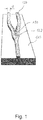
- Fig. 1 shows a photonic integrated circuit according to an embodiment of the present invention.
- the circuit comprises: a dielectric substrate 110; a dielectric waveguide arrangement 120 on the substrate 110 for guiding terahertz (THz) waves and a local functionalization 130 which has a metallization in a surface area of the dielectric waveguide arrangement 120.
- the metallization 130 is localized along a propagation direction of the THz waves to allow metallization-free propagation of the THz wave outside the local functionalization.
- the waveguide arrangement 120 comprises a bifurcation having a branching point 123 and the surface area of the local functionalization 130 is formed by opposing surfaces adjacent to the branching point 123.
- This structure can be used, for example, as a beam splitter, wherein the metallic structure 130 improves the beam splitting property and makes the beam splitter broadband while keeping the splitting factor as constant as possible.
- the dielectric waveguide arrangement 120 here and in other embodiments can have an extension d perpendicular to the propagation direction of a THz wave, which is in a range from 10 ⁇ m to 300 ⁇ m or in a range from 30 ⁇ m to 100 ⁇ m.
- the material of the waveguide 120 has a refraction index (refraction number) that is at least 1.5 as high as a refraction index of the dielectric substrate 110, in order to keep the THz wave efficiently in the waveguide 120.
- the waveguide 120 and its surroundings should be mostly pure dielectric.
- the circuit could of course have further distant metallic structures.
- the desired metallization-free propagation should mean that the THz wave is not influenced by free charge carriers, as they occur in metals as well as in other guides. Since free, easily movable charge carriers, which are present in large numbers in metals, force a null of the electric field strength (they are field-free inside), higher modes are suppressed or at least shifted (away from the metallization) by the metallization.
- the metallization sets even modes to null, while odd modes are suppressed with increasing height, as their maxima increasingly approach the metallization. All these effects lead to losses that avoid embodiments or that are used specifically for functionalization.
- Fig. 2 shows a further embodiment of the photonic integrated circuit, which has an exemplary diode 140 for generating a THz oscillation.
- the waveguide arrangement 120 is formed as a Vivaldi antenna which couples to the diode 140 and, starting from the diode 140, has a widening opening portion 125 for radiating a coupled THz wave.
- the metallization 130 is formed here on both sides of the widening opening portion 125 to support a coupling of the THz oscillation from the diode 140 into the Vivaldi antenna.
- This embodiment shows only as an example a THz emitter diode as a possible active element, which couples power with a Vivaldi antenna into an underlying dielectric waveguide.
- other active elements can also be efficiently coupled to the waveguide arrangement 110 by means of local functionalization 130.
- Fig. 3 shows a further embodiment of the photonic integrated circuit, which has at least one THz resonator 150.
- the resonator 150 also has a dielectric material having a higher refraction number than the substrate 110 and is arranged along the substrate 110 laterally offset from the waveguide arrangement 120.
- a gap 135 can be formed between the resonator 150 and the waveguide arrangement 120 in such a manner that there is no direct contact between the two components.
- the resonator 150 can, for example, be formed from the same material as the waveguide 120.
- an optional underlay 160 is also formed on a back side of the substrate 110 (on a side of the substrate 110 opposing the THz resonator 150).
- Such an underlay 160 provides not only mechanical support or hold, but can also provide shielding from external influences that could interfere with the photonic signals.
- Such an underlay/shielding layer can also be formed in the embodiments from Fig. 1 or Fig. 2 .
- This shielding layer/underlay may have a metal, for example, wherein the distance to the waveguide should be chosen sufficiently large (distance of at least a plurality of THz wavelengths) such that the influence on the THz wave is negligible due to the exponential damping.
- the metallization 130 is in turn only formed locally in an area 135, namely where the distance between the waveguide arrangement 120 and the THz resonator 150 is the smallest.
- the metallization 130 can again be formed on a surface of the waveguide arrangement 120 which is opposing the substrate 110 and/or the THz resonator 150. With this metallization 130, in turn, certain modes of the THz waves are specifically suppressed or the wave is formed in such a manner that it migrates towards the resonator 150, which facilitates the coupling.
- the purely dielectric resonator 150 which was locally functionalized by means of metallization 130, therefore couples efficiently to the dielectric waveguide 120, the metallization layer 130 on the waveguide 120 pushes the mode towards the resonator 150 to improve the coupling.
- Embodiments have a number of advantages over conventional circuits.
- these are based on the combination of dielectric waveguide structures 120, which are similar to optical photonic integrated circuits, and the metallic structures 130, which can be manufactured by contact lithography or similar lithography techniques. Therefore, a considerable scalability is already given.
- the wave guidance occurs primarily in the low-loss dielectric (the waveguide 120), while the metallic additives (metallizations 130 as functionalizations) reduce the losses, e.g. in curved structures (as in Fig. 1 ), suppress undesired modes or simply allow interfaces to other components (as in Fig. 2 or Fig. 3 ).
- the metallic additives metallic additives 130 as functionalizations
- reduce the losses e.g. in curved structures (as in Fig. 1 ), suppress undesired modes or simply allow interfaces to other components (as in Fig. 2 or Fig. 3 ).
- GSG ground-signal-ground
- a mixture of metallic and dielectric structures can also provide advantages for the improved radiation (emission).
- the invention does not require that metallic structures 130 be present everywhere on the waveguide 120. They are mainly used to improve desired properties such as the components integrated into the waveguide structure 120.
- the functionalization 130 (e.g. metallization) could be on both sides of the dielectric waveguide arrangement 120.
- the functionalization 130 is formed directly on the surface of the dielectric waveguide arrangement 120 (e.g. by evaporation on the waveguide arrangement 120). Since a metal surface sets the electric field to zero, the metallization directly on the waveguide arrangement 120 will yield the desired functionalization 130 by the interaction of the electro-magnetic wave in the waveguide 120 with the surface of the waveguide 120.
- the exemplary metallization 130 may not generate an electric field strength in the dielectric waveguide arrangement 120.
- no voltage is applied on or between components of the metallization 130, but, optionally, they may be set on a common voltage level (e.g. ground) or its potential level is freely floating.
- the dielectric waveguide arrangement 120 comprises a material with a refractive index that maybe independent of an external electric field (DC or AC).
- an DC and/or AC voltage may be applied on or between the metal components of the functionalization 130, which is formed directly on the surface of the dielectric waveguide arrangement 120.
- the manufacture of the structures can be performed with a variety of methods, e.g. UV contact lithography, UV projection lithography, UV laser lithography, laser ablation, electron beam lithography, possibly even additive manufacturing, as far as low-loss dielectrics become printable, and more.
- a further material similar to the material having a lower refraction number (substrate 110) can be applied to the structured sample.
- the waveguide arrangement 120 can therefore be arranged between two dielectric substrates having a low refraction number (e.g. less than half of the refraction number of the waveguide material 120).
- further metallic structures can optionally be applied to the substrate 120 (material of lower refraction number).
- the upper layer and the lower layer can consist of materials of the same or very similar refraction number, while the middle material should have a significantly higher refraction number. This allows for a significant increase in bandwidth, as substrate modes are suppressed.
Landscapes
- Engineering & Computer Science (AREA)
- Physics & Mathematics (AREA)
- Manufacturing & Machinery (AREA)
- Microelectronics & Electronic Packaging (AREA)
- General Physics & Mathematics (AREA)
- Optics & Photonics (AREA)
- Optical Integrated Circuits (AREA)
Applications Claiming Priority (1)
| Application Number | Priority Date | Filing Date | Title |
|---|---|---|---|
| DE102019104982.2A DE102019104982A1 (de) | 2019-02-27 | 2019-02-27 | Photonische Integrierte Schaltung |
Publications (2)
| Publication Number | Publication Date |
|---|---|
| EP3726643A2 true EP3726643A2 (de) | 2020-10-21 |
| EP3726643A3 EP3726643A3 (de) | 2020-12-23 |
Family
ID=69740181
Family Applications (1)
| Application Number | Title | Priority Date | Filing Date |
|---|---|---|---|
| EP20159446.2A Withdrawn EP3726643A3 (de) | 2019-02-27 | 2020-02-26 | Photonische integrierte schaltung |
Country Status (4)
| Country | Link |
|---|---|
| US (1) | US11239538B2 (de) |
| EP (1) | EP3726643A3 (de) |
| CN (1) | CN111624704B (de) |
| DE (1) | DE102019104982A1 (de) |
Families Citing this family (1)
| Publication number | Priority date | Publication date | Assignee | Title |
|---|---|---|---|---|
| CN115548616B (zh) * | 2022-12-01 | 2023-03-21 | 四川太赫兹通信有限公司 | 一种太赫兹电路的构造元件、构造系统及电路系统 |
Family Cites Families (13)
| Publication number | Priority date | Publication date | Assignee | Title |
|---|---|---|---|---|
| US3995238A (en) * | 1975-06-30 | 1976-11-30 | Epsilon Lambda Electronics Corporation | Image waveguide transmission line and mode launchers utilizing same |
| US4677404A (en) * | 1984-12-19 | 1987-06-30 | Martin Marietta Corporation | Compound dielectric multi-conductor transmission line |
| WO2009111610A1 (en) * | 2008-03-05 | 2009-09-11 | University Of Washington | Waveguides and devices for enhanced third order nonlinearities in polymer-silicon systems |
| US20130265733A1 (en) * | 2012-04-04 | 2013-10-10 | Texas Instruments Incorporated | Interchip communication using an embedded dielectric waveguide |
| US9112253B2 (en) * | 2013-03-19 | 2015-08-18 | Texas Instruments Incorporated | Dielectric waveguide combined with electrical cable |
| US9472840B2 (en) * | 2013-06-12 | 2016-10-18 | Texas Instruments Incorporated | Dielectric waveguide comprised of a core, a cladding surrounding the core and cylindrical shape conductive rings surrounding the cladding |
| US9568675B2 (en) * | 2013-07-03 | 2017-02-14 | City University Of Hong Kong | Waveguide coupler |
| CN103682534B (zh) * | 2013-12-26 | 2016-05-04 | 航天恒星科技有限公司 | 一种缺陷地加载磁耦合结构的介质波导滤波器 |
| US9515363B2 (en) * | 2014-04-09 | 2016-12-06 | Texas Instruments Incorporated | Dielectric waveguide (DWG) filter having curved first and second DWG branches where the first branch forms a delay line that rejoins the second branch |
| CN104103882B (zh) * | 2014-07-15 | 2017-08-08 | 电子科技大学 | 一种太赫兹介质填充金属槽波导 |
| CN106054291B (zh) * | 2016-06-16 | 2018-03-30 | 北京大学 | 混合型的金属‑介质ssp周期光栅系统及其用途和方法 |
| CN108020873B (zh) * | 2017-11-29 | 2020-03-31 | 东南大学 | 一种光子集成电路中八边形金属纳米光学天线 |
| CN108152870B (zh) * | 2017-12-27 | 2020-07-31 | 东南大学 | 一种光子集成电路中双领结金属纳米光学天线 |
-
2019
- 2019-02-27 DE DE102019104982.2A patent/DE102019104982A1/de active Pending
-
2020
- 2020-02-20 US US16/796,343 patent/US11239538B2/en active Active
- 2020-02-26 CN CN202010120352.6A patent/CN111624704B/zh active Active
- 2020-02-26 EP EP20159446.2A patent/EP3726643A3/de not_active Withdrawn
Also Published As
| Publication number | Publication date |
|---|---|
| US20200274220A1 (en) | 2020-08-27 |
| CN111624704B (zh) | 2024-10-01 |
| US11239538B2 (en) | 2022-02-01 |
| DE102019104982A1 (de) | 2020-08-27 |
| EP3726643A3 (de) | 2020-12-23 |
| CN111624704A (zh) | 2020-09-04 |
Similar Documents
| Publication | Publication Date | Title |
|---|---|---|
| Cong et al. | Spatiotemporal dielectric metasurfaces for unidirectional propagation and reconfigurable steering of terahertz beams | |
| US11374294B2 (en) | Tunable phase shifter wherein phase shift is changed by varying a distance between an image guide and a dielectric perturber | |
| Zhang et al. | High‐efficiency circularly polarised leaky‐wave antenna fed by spoof surface plasmon polaritons | |
| US9219298B2 (en) | Removal of spurious microwave modes via flip-chip crossover | |
| US7692516B2 (en) | Phase shifter with photonic band gap structure using ferroelectric thin film | |
| Merlo et al. | Wireless communication system via nanoscale plasmonic antennas | |
| KR102031058B1 (ko) | 물리적 접촉 방식의 그래핀 전-광 변조기 및 이를 제조하는 방법 | |
| Luo et al. | Tunable surface-plasmon-polariton filter constructed by corrugated metallic line and high permittivity material | |
| US11239538B2 (en) | Photonic integrated circuit comprising a dielectric waveguide on a substrate including a local functionalization to enable metallization-free THz wave propagation | |
| Rezaee et al. | Dirac leaky wave antenna for millimetre‐wave applications | |
| Der et al. | Design and characterization of W-band silicon micromachined high-power and high-speed photoconductive evanescent-mode waveguide single and double throw switches | |
| CN120660451A (zh) | 一种用于生产电气线路布置的方法和电气线路布置 | |
| Mahdian et al. | THz multimode interference power divider based on groove gap waveguide configuration | |
| Tajik et al. | Dielectric resonator antenna fed by photonic crystal waveguide based on silicon-on-glass technology | |
| Li et al. | Narrow beam and low-sidelobe electro-optic beam steering on thin-film lithium niobate optical phased array | |
| Shireen et al. | CPW to Rectangular Waveguide Transition on an ${\hbox {LiNbO}} _ {3} $ Substrate | |
| Zheng et al. | Continuously tunable topological negative refraction via a tailorable Bloch wavevector in momentum space | |
| Gao et al. | Plasmonic Luneburg and Eaton lenses for terahertz spoof surface plasmon polaritons | |
| Chen et al. | Broadband graphene modulator with high modulation depth based on tip plasmonic waveguide | |
| Koul et al. | Microwave Integrated Circuits Based on Spoof Surface Plasmon Polariton | |
| RU2663266C1 (ru) | Зонд ближнепольного микроскопа | |
| Kumar et al. | Photonic crystal assisted multiband compact terahertz antenna on engineered silicon‐on‐insulator | |
| Minasian et al. | Integrated Microwave Photonic Signal Processing and Sensing | |
| Ramirez et al. | Electro Optical Waveguide Based on Embedded Double-Monolayer Graphene Capacitor | |
| Salhi et al. | Multilayer integration platform with low propagation and transition losses for dense optical phased arrays |
Legal Events
| Date | Code | Title | Description |
|---|---|---|---|
| PUAI | Public reference made under article 153(3) epc to a published international application that has entered the european phase |
Free format text: ORIGINAL CODE: 0009012 |
|
| STAA | Information on the status of an ep patent application or granted ep patent |
Free format text: STATUS: THE APPLICATION HAS BEEN PUBLISHED |
|
| AK | Designated contracting states |
Kind code of ref document: A2 Designated state(s): AL AT BE BG CH CY CZ DE DK EE ES FI FR GB GR HR HU IE IS IT LI LT LU LV MC MK MT NL NO PL PT RO RS SE SI SK SM TR |
|
| AX | Request for extension of the european patent |
Extension state: BA ME |
|
| PUAL | Search report despatched |
Free format text: ORIGINAL CODE: 0009013 |
|
| AK | Designated contracting states |
Kind code of ref document: A3 Designated state(s): AL AT BE BG CH CY CZ DE DK EE ES FI FR GB GR HR HU IE IS IT LI LT LU LV MC MK MT NL NO PL PT RO RS SE SI SK SM TR |
|
| AX | Request for extension of the european patent |
Extension state: BA ME |
|
| RIC1 | Information provided on ipc code assigned before grant |
Ipc: H01P 5/12 20060101ALI20201118BHEP Ipc: H01P 7/10 20060101ALI20201118BHEP Ipc: H01P 5/08 20060101ALI20201118BHEP Ipc: H01P 3/16 20060101AFI20201118BHEP Ipc: G02B 6/12 20060101ALI20201118BHEP |
|
| STAA | Information on the status of an ep patent application or granted ep patent |
Free format text: STATUS: THE APPLICATION IS DEEMED TO BE WITHDRAWN |
|
| 18D | Application deemed to be withdrawn |
Effective date: 20210824 |