EP3726589A1 - Single toe interconnect - Google Patents
Single toe interconnect Download PDFInfo
- Publication number
- EP3726589A1 EP3726589A1 EP20168447.9A EP20168447A EP3726589A1 EP 3726589 A1 EP3726589 A1 EP 3726589A1 EP 20168447 A EP20168447 A EP 20168447A EP 3726589 A1 EP3726589 A1 EP 3726589A1
- Authority
- EP
- European Patent Office
- Prior art keywords
- interconnects
- solar cell
- toe
- edge
- solar cells
- Prior art date
- Legal status (The legal status is an assumption and is not a legal conclusion. Google has not performed a legal analysis and makes no representation as to the accuracy of the status listed.)
- Pending
Links
Images





Classifications
-
- H—ELECTRICITY
- H10—SEMICONDUCTOR DEVICES; ELECTRIC SOLID-STATE DEVICES NOT OTHERWISE PROVIDED FOR
- H10F—INORGANIC SEMICONDUCTOR DEVICES SENSITIVE TO INFRARED RADIATION, LIGHT, ELECTROMAGNETIC RADIATION OF SHORTER WAVELENGTH OR CORPUSCULAR RADIATION
- H10F77/00—Constructional details of devices covered by this subclass
- H10F77/93—Interconnections
- H10F77/933—Interconnections for devices having potential barriers
- H10F77/935—Interconnections for devices having potential barriers for photovoltaic devices or modules
-
- H—ELECTRICITY
- H10—SEMICONDUCTOR DEVICES; ELECTRIC SOLID-STATE DEVICES NOT OTHERWISE PROVIDED FOR
- H10F—INORGANIC SEMICONDUCTOR DEVICES SENSITIVE TO INFRARED RADIATION, LIGHT, ELECTROMAGNETIC RADIATION OF SHORTER WAVELENGTH OR CORPUSCULAR RADIATION
- H10F19/00—Integrated devices, or assemblies of multiple devices, comprising at least one photovoltaic cell covered by group H10F10/00, e.g. photovoltaic modules
- H10F19/90—Structures for connecting between photovoltaic cells, e.g. interconnections or insulating spacers
-
- B—PERFORMING OPERATIONS; TRANSPORTING
- B64—AIRCRAFT; AVIATION; COSMONAUTICS
- B64G—COSMONAUTICS; VEHICLES OR EQUIPMENT THEREFOR
- B64G1/00—Cosmonautic vehicles
- B64G1/22—Parts of, or equipment specially adapted for fitting in or to, cosmonautic vehicles
- B64G1/42—Arrangements or adaptations of power supply systems
- B64G1/44—Arrangements or adaptations of power supply systems using radiation, e.g. deployable solar arrays
- B64G1/443—Photovoltaic cell arrays
-
- H—ELECTRICITY
- H10—SEMICONDUCTOR DEVICES; ELECTRIC SOLID-STATE DEVICES NOT OTHERWISE PROVIDED FOR
- H10F—INORGANIC SEMICONDUCTOR DEVICES SENSITIVE TO INFRARED RADIATION, LIGHT, ELECTROMAGNETIC RADIATION OF SHORTER WAVELENGTH OR CORPUSCULAR RADIATION
- H10F19/00—Integrated devices, or assemblies of multiple devices, comprising at least one photovoltaic cell covered by group H10F10/00, e.g. photovoltaic modules
- H10F19/20—Integrated devices, or assemblies of multiple devices, comprising at least one photovoltaic cell covered by group H10F10/00, e.g. photovoltaic modules comprising photovoltaic cells in arrays in or on a single semiconductor substrate, the photovoltaic cells having planar junctions
-
- H—ELECTRICITY
- H10—SEMICONDUCTOR DEVICES; ELECTRIC SOLID-STATE DEVICES NOT OTHERWISE PROVIDED FOR
- H10F—INORGANIC SEMICONDUCTOR DEVICES SENSITIVE TO INFRARED RADIATION, LIGHT, ELECTROMAGNETIC RADIATION OF SHORTER WAVELENGTH OR CORPUSCULAR RADIATION
- H10F19/00—Integrated devices, or assemblies of multiple devices, comprising at least one photovoltaic cell covered by group H10F10/00, e.g. photovoltaic modules
- H10F19/90—Structures for connecting between photovoltaic cells, e.g. interconnections or insulating spacers
- H10F19/902—Structures for connecting between photovoltaic cells, e.g. interconnections or insulating spacers for series or parallel connection of photovoltaic cells
-
- H—ELECTRICITY
- H10—SEMICONDUCTOR DEVICES; ELECTRIC SOLID-STATE DEVICES NOT OTHERWISE PROVIDED FOR
- H10F—INORGANIC SEMICONDUCTOR DEVICES SENSITIVE TO INFRARED RADIATION, LIGHT, ELECTROMAGNETIC RADIATION OF SHORTER WAVELENGTH OR CORPUSCULAR RADIATION
- H10F19/00—Integrated devices, or assemblies of multiple devices, comprising at least one photovoltaic cell covered by group H10F10/00, e.g. photovoltaic modules
- H10F19/90—Structures for connecting between photovoltaic cells, e.g. interconnections or insulating spacers
- H10F19/902—Structures for connecting between photovoltaic cells, e.g. interconnections or insulating spacers for series or parallel connection of photovoltaic cells
- H10F19/904—Structures for connecting between photovoltaic cells, e.g. interconnections or insulating spacers for series or parallel connection of photovoltaic cells characterised by the shapes of the structures
-
- H—ELECTRICITY
- H10—SEMICONDUCTOR DEVICES; ELECTRIC SOLID-STATE DEVICES NOT OTHERWISE PROVIDED FOR
- H10F—INORGANIC SEMICONDUCTOR DEVICES SENSITIVE TO INFRARED RADIATION, LIGHT, ELECTROMAGNETIC RADIATION OF SHORTER WAVELENGTH OR CORPUSCULAR RADIATION
- H10F71/00—Manufacture or treatment of devices covered by this subclass
-
- H—ELECTRICITY
- H10—SEMICONDUCTOR DEVICES; ELECTRIC SOLID-STATE DEVICES NOT OTHERWISE PROVIDED FOR
- H10F—INORGANIC SEMICONDUCTOR DEVICES SENSITIVE TO INFRARED RADIATION, LIGHT, ELECTROMAGNETIC RADIATION OF SHORTER WAVELENGTH OR CORPUSCULAR RADIATION
- H10F77/00—Constructional details of devices covered by this subclass
- H10F77/93—Interconnections
- H10F77/933—Interconnections for devices having potential barriers
- H10F77/935—Interconnections for devices having potential barriers for photovoltaic devices or modules
- H10F77/937—Busbar structures for modules
-
- H—ELECTRICITY
- H10—SEMICONDUCTOR DEVICES; ELECTRIC SOLID-STATE DEVICES NOT OTHERWISE PROVIDED FOR
- H10F—INORGANIC SEMICONDUCTOR DEVICES SENSITIVE TO INFRARED RADIATION, LIGHT, ELECTROMAGNETIC RADIATION OF SHORTER WAVELENGTH OR CORPUSCULAR RADIATION
- H10F77/00—Constructional details of devices covered by this subclass
- H10F77/80—Arrangements for preventing damage to photovoltaic cells caused by corpuscular radiation, e.g. for space applications
-
- Y—GENERAL TAGGING OF NEW TECHNOLOGICAL DEVELOPMENTS; GENERAL TAGGING OF CROSS-SECTIONAL TECHNOLOGIES SPANNING OVER SEVERAL SECTIONS OF THE IPC; TECHNICAL SUBJECTS COVERED BY FORMER USPC CROSS-REFERENCE ART COLLECTIONS [XRACs] AND DIGESTS
- Y02—TECHNOLOGIES OR APPLICATIONS FOR MITIGATION OR ADAPTATION AGAINST CLIMATE CHANGE
- Y02E—REDUCTION OF GREENHOUSE GAS [GHG] EMISSIONS, RELATED TO ENERGY GENERATION, TRANSMISSION OR DISTRIBUTION
- Y02E10/00—Energy generation through renewable energy sources
- Y02E10/50—Photovoltaic [PV] energy
Definitions
- the disclosure is related generally to a single toe interconnect for solar cells.
- the current In order to make use of electrical power generated by solar cells from sunlight, the current must be transported from the solar cell to the external circuit. This is typically done using metal gridlines (fine features collecting current from all areas of the device), one or more busbars (larger feature aggregating current from many gridlines), contact pads (locations to attach tabs/interconnects to connect to other devices), and interconnects to span between the contact pads and other devices. These grids, busbars, contact pads, tabs and interconnects all result in parasitic losses.
- the metal used for grids, busbars, contact pads and interconnects also imposes power losses on the solar cell's conversion efficiency, by preventing light from reaching the semiconductor layers of the solar cell, from parasitic losses, and with series resistance.
- metal coverage of the solar cell is the primary loss factor. Optimization of gridlines and busbar designs is standard practice to reduce obscuration, but the design and location of contacts and interconnects has received little attention.
- Space solar cells typically have two or three interconnects spaced as widely apart as possible. This common practice is intended to reduce the risk of an open circuit if a solar cell cracks, but also results in current flowing relatively long distances along the busbars. Removal of an interconnect for large-format solar cells is known to cause efficiency loss. For example, the most recent evolution has been to reduce interconnects from three to two for all solar cells with an area less than 65 cm 2 , with the remaining two interconnects being placed as widely apart as possible.
- interconnects increase resistance losses when conducting current to the interconnects and/or result in increased dimensions of the busbars that reduces cell current.
- widely spaced interconnects increase the risk that cell cracks could isolate all interconnects, creating on open circuit.
- interconnects only being available in multiples of two leads to over- or under-designed solutions.
- the present disclosure describes an interconnect for making electrical connections for a solar cell, wherein the interconnect consists of a single toe, without a second toe connected to the single toe, and with no connected crossbars.
- the present disclosure also describes a method for fabricating the interconnect and a method for making electrical connections using the interconnect.
- the interconnect is comprised of one or more layers of conductive, bondable material, selected from aluminum (Al), copper (Cu), silver (Ag), gold (Au), molybdenum (Mo), Kovar® (an iron-nickel-cobalt alloy), Invar (64FeNi), or an alloy or combination thereof.
- the interconnect is about 0.25 to 1 inch in length, 40 to 100 mils in width, and 1 to 2 mils in thickness.
- a plurality of the interconnects may be placed uniformly across an edge of the solar cell.
- three interconnects are placed uniformly across an edge of the solar cell, when the solar cell has an area less than 60 cm 2 .
- four or more interconnects are placed uniformly across an edge of the solar cell, when the solar cell has an area greater than 60 cm 2 .
- This disclosure improves electrical connections between solar cells by replacing relatively fewer, large interconnects with relatively more, smaller interconnects.
- space-grade interconnects are comprised of two parallel flat metal "toes" or “legs” connected with crossbars.
- an interconnect consists of a single flat metal toe, without a second toe, and with no connected crossbars.
- interconnects with only a single toe allows the number of interconnects to be properly sized to the cell and program, including odd numbers of interconnects.
- Removing the crossbars allows interconnects to be placed more uniformly across the solar cell's edges, increasing solar cell efficiency, reducing material cost, improving reliability and enabling advanced manufacturing, such as real-time laser cutting of interconnects.
- FIG. 1A illustrates a solar cell 10 and the interconnects 12 used to transmit the electrical power generated by the solar cell 10.
- the solar cell 10 includes metal gridlines 14 collecting current from all areas of the solar cell 10, one or more busbars 16 aggregating current from the gridlines 14, contact pads 18 used to attach the interconnects 12 to span between the contact pads 18 and other devices (not shown).
- space solar cells 10 typically have 2 or 3 interconnects 12 spaced as widely apart as possible. This common practice is intended to reduce the risk of an open circuit if a solar cell cracks, but also results in current flowing relatively long distances along the busbar 16. However, customers have been known to remove an interconnect 12 for large-format cells 10, which is known to cause efficiency losses.
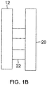
- FIG. 1B illustrates a configuration for one interconnect 12.
- the interconnect 12 is comprised of two thin flat metal toes or legs 20 positioned in parallel with two or more crossbars 22 holding the two toes 20 in place. The need to provide weld redundancy is why double toes 20 are used.
- This disclosure overcomes these limitations by providing a new design for an improved interconnect with a single toe or leg, and distributing the interconnects relatively uniformly across an edge of the solar cell.
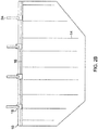
- FIGS. 2A , 2B and 2C An apparatus, method of fabricating and method of making electrical connections using this new design are illustrated in FIGS. 2A , 2B and 2C , wherein FIG. 2A shows an interconnect 24 for making electrical connections for the solar cell 10, the interconnect 24 consisting of a single toe 26, without a second toe 20 connected to the single toe 26, and with no connected crossbars 22; FIG. 2B illustrates a plurality, i.e., four, of the interconnects 24 placed uniformly along an edge of the solar cell 10; and FIG. 2C illustrates a plurality, i.e., five, of the interconnects 24 placed uniformly along an edge of the solar cell 10.
- FIGS. 2A , 2B and 2C An apparatus, method of fabricating and method of making electrical connections using this new design are illustrated in FIGS. 2A , 2B and 2C , wherein FIG. 2A shows an interconnect 24 for making electrical connections for the solar cell 10, the interconnect 24 consisting of a single
- the interconnect 24 is comprised of one or more layers of conductive, bondable material, for example, in the form of a metal foil, selected from aluminum (Al), copper (Cu), silver (Ag), gold (Au), molybdenum (Mo), Kovar® (an iron-nickel-cobalt alloy), Invar (64FeNi), or an alloy, or combination thereof.
- the interconnect 24 may be about 0.25 to 1 inch in length, 40 to 100 mils in width, and 1 to 2 mils in thickness.
- the plurality of the interconnects comprise three interconnects 24 placed uniformly, i.e., with equal space between each interconnect 24, across an edge of the solar cell 10, when the solar cell 10 has an area less than 60 cm 2 .
- the plurality of the interconnects 24 comprise four or more interconnects 24 placed uniformly across an edge of the solar cell 10, when the solar cell 10 has an area greater than 60 cm 2 .
- This interconnect 24 reduces both current and voltage losses in the busbars 16, while reducing assembly attrition and maintaining risk mitigation against open circuits. The result is improved efficiency, reduced parasitic loss, and improved manufacturability by eliminating the double toe interconnects 12 with connected crossbars 22.
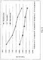
- FIG. 3 is a graph of relative power loss (i.e., resistance loss, obscuration, and total power loss) for a solar cell 10 with an area greater than 70 cm 2 with different numbers and types of interconnects (lower power loss is better), including a 3x double toe interconnect (IC) 12, 4x single toe IC 24, 5x single toe IC 24, 6x single toe IC 24, and 8x 20 mil wire bond.
- IC 3x double toe interconnect
- 4x single toe IC 24 5x single toe IC 24, 6x single toe IC 24, and 8x 20 mil wire bond.
- the reduced metal used for the interconnect 24 may increase the potential for damage.
- use of the single toe interconnects 24 between solar cells 10 provides a number of benefits, including increased redundancy, reduced assembly attrition, more flexible design options, increased reliability, improved efficiency, reduced material cost, and advanced manufacturing.
- the number of interconnections can be increased using the single toe interconnects 24 to increase redundancy.
- the number of interconnections using the single toe interconnects 24 can be decreased to reduce assembly attrition.
- This disclosure provides more flexible design options, in that the solar cell 10 can have more points of interconnection (more redundancy) or fewer points of interconnection (reduced assembly attrition) using the new interconnects 24.
- this disclosure provides more design freedom to select the number of interconnections and the location of those interconnections using the new interconnects 24. For example, odd numbers of interconnections for the solar cell 10 are possible using the interconnects 24, whereas the interconnects 12 always result in even numbers of interconnections due to the double toes 20.
- This disclosure can provide equal, greater, or less reliability than currently required as determined by the number, spacing and/or locations of interconnects 24.
- the number, spacing and locations of the interconnections can be selected to improve solar cell 10 efficiency (evenly spaced) or positioned based on some other constraints.
- the location of interconnections using the interconnects 24 are not constrained by the crossbars 22.
- Removing the crossbars 22 allows the interconnects 24 to be placed more uniformly across the edges of the solar cell 10, which simultaneously increases solar cell 10 efficiency, reduces material cost, and improves reliability. For example, even spacing of interconnects 24 leads to improved reliability by reducing the probability that solar cell 10 cracks can electrically isolate the interconnects 24 to create an open circuit. Even spacing of interconnects 24 also leads to higher solar cell 10 efficiency due to reduced busbar 16 obscuration and resistance losses.
- Single toe interconnects 24 inherently reduce the amount of material consumed in fabrication and therefore the cost of the interconnect 24.
- the crossbars 22 increase material consumption and cost of interconnects 12, and increases obscuration for contact pads 18 on a solar cell 10.
- Single toe interconnects 24 are more compatible with advanced manufacturing concepts, such as real-time laser cutting of the interconnects 24 from raw stock material.
- Single-toe interconnects 24 also provide mechanical stress relief for the solar cell 10.
- Examples of the disclosure may be described in the context of a method 28 of fabricating one or more interconnects 24, a solar cell 10 using the interconnects 24, a solar cell panel comprised of the solar cells 10, and/or a space vehicle such as a satellite including the solar cell panel, comprising steps 30-42, as shown in FIG. 4A , wherein the resulting satellite 44 comprised of various systems 46 and a body 48, including a panel 50 comprised of an array 52 of one or more solar cells 10 is shown in FIG. 4B .
- exemplary method 28 may include specification and design 30 of the satellite 44, and material procurement 32 for same.
- component and subassembly manufacturing 34 and system integration 36 of the satellite 44 takes place, which include fabricating the satellite 44, panel 50, array 52 and solar cells 10.
- the satellite 44 may go through certification and delivery 38 in order to be placed in service 40.
- the satellite 44 may also be scheduled for maintenance and service 42 (which includes modification, reconfiguration, refurbishment, and so on), before being launched.
- a system integrator may include without limitation any number of manufacturers and major-system subcontractors; a third party may include without limitation any number of venders, subcontractors, and suppliers; and an operator may be a satellite company, military entity, service organization, and so on.
- the satellite 44 fabricated by exemplary method 28 may include various systems 46 and a body 48.
- the systems 46 included with the satellite 44 include, but are not limited to, one or more of a propulsion system 54, an electrical system 56, a communications system 58, and a power system 60. Any number of other systems also may be included.
- FIG. 5 is an illustration of the panel 50 in the form of a functional block diagram, according to one example.
- the panel 50 is comprised of the array 52, which is comprised of one or more of the solar cells 10 individually attached to the panel 50.
- Each of the solar cells 10 absorbs light 62 from a light source 64 and generates an electrical output 66 in response thereto.
- At least one of the solar cells 10 includes at least the metal gridlines 14 collecting current from all areas of the solar cell 10, the busbars 16 aggregating current from the gridlines 14, and contact pads 18 used to attach the interconnects 24 to span between the contact pads 18 and other devices (not shown) for making electrical connections.
Landscapes
- Engineering & Computer Science (AREA)
- Life Sciences & Earth Sciences (AREA)
- Sustainable Development (AREA)
- Remote Sensing (AREA)
- Aviation & Aerospace Engineering (AREA)
- Photovoltaic Devices (AREA)
Abstract
Description
- The disclosure is related generally to a single toe interconnect for solar cells.
- In order to make use of electrical power generated by solar cells from sunlight, the current must be transported from the solar cell to the external circuit. This is typically done using metal gridlines (fine features collecting current from all areas of the device), one or more busbars (larger feature aggregating current from many gridlines), contact pads (locations to attach tabs/interconnects to connect to other devices), and interconnects to span between the contact pads and other devices. These grids, busbars, contact pads, tabs and interconnects all result in parasitic losses.
- The metal used for grids, busbars, contact pads and interconnects also imposes power losses on the solar cell's conversion efficiency, by preventing light from reaching the semiconductor layers of the solar cell, from parasitic losses, and with series resistance. For state-of-the-art space solar cells, metal coverage of the solar cell is the primary loss factor. Optimization of gridlines and busbar designs is standard practice to reduce obscuration, but the design and location of contacts and interconnects has received little attention.
- Space solar cells typically have two or three interconnects spaced as widely apart as possible. This common practice is intended to reduce the risk of an open circuit if a solar cell cracks, but also results in current flowing relatively long distances along the busbars. Removal of an interconnect for large-format solar cells is known to cause efficiency loss. For example, the most recent evolution has been to reduce interconnects from three to two for all solar cells with an area less than 65 cm2, with the remaining two interconnects being placed as widely apart as possible.
- However, widely spaced interconnects increase resistance losses when conducting current to the interconnects and/or result in increased dimensions of the busbars that reduces cell current. Moreover, widely spaced interconnects increase the risk that cell cracks could isolate all interconnects, creating on open circuit. In addition, interconnects only being available in multiples of two leads to over- or under-designed solutions.
- Thus, there is a need in the art for improved solar cell interconnects. The present disclosure satisfies this need.
- To overcome the limitations described above, and to overcome other limitations that will become apparent upon reading and understanding the present specification, the present disclosure describes an interconnect for making electrical connections for a solar cell, wherein the interconnect consists of a single toe, without a second toe connected to the single toe, and with no connected crossbars. The present disclosure also describes a method for fabricating the interconnect and a method for making electrical connections using the interconnect.
- The interconnect is comprised of one or more layers of conductive, bondable material, selected from aluminum (Al), copper (Cu), silver (Ag), gold (Au), molybdenum (Mo), Kovar® (an iron-nickel-cobalt alloy), Invar (64FeNi), or an alloy or combination thereof. The interconnect is about 0.25 to 1 inch in length, 40 to 100 mils in width, and 1 to 2 mils in thickness.
- A plurality of the interconnects may be placed uniformly across an edge of the solar cell. In one example, three interconnects are placed uniformly across an edge of the solar cell, when the solar cell has an area less than 60 cm2. In another example, four or more interconnects are placed uniformly across an edge of the solar cell, when the solar cell has an area greater than 60 cm2.
- Referring now to the drawings in which like reference numbers represent corresponding parts throughout:
-
FIG. 1A illustrates a typical solar cell and the interconnects used to transmit electrical power generated by the solar cell. -
FIG. 1B illustrates a typical configuration for one interconnect. -
FIG. 2A shows an interconnect consisting of a single toe, without a second toe and with no crossbars. -
FIG. 2B illustrates the placement of four interconnects along one edge of a solar cell. -
FIG. 2C illustrates the placement of five interconnects along one edge of a solar cell. -
FIG. 3 is a graph of relative power loss (i.e., resistance loss, obscuration, and total power loss) for a solar cell with different numbers and types of interconnects. -
FIG. 4A illustrates a method of fabricating a solar cell, solar cell panel and/or satellite. -
FIG. 4B illustrates a resulting satellite having a solar cell panel comprised of solar cells. -
FIG. 5 is an illustration of the solar cell panel in the form of a functional block diagram. - In the following description, reference is made to the accompanying drawings which form a part hereof, and in which is shown by way of illustration a specific example in which the disclosure may be practiced. It is to be understood that other examples may be utilized and structural changes may be made without departing from the scope of the present disclosure.
- This disclosure improves electrical connections between solar cells by replacing relatively fewer, large interconnects with relatively more, smaller interconnects. Currently, space-grade interconnects are comprised of two parallel flat metal "toes" or "legs" connected with crossbars. In this disclosure, an interconnect consists of a single flat metal toe, without a second toe, and with no connected crossbars.
- Making interconnects with only a single toe allows the number of interconnects to be properly sized to the cell and program, including odd numbers of interconnects. Removing the crossbars allows interconnects to be placed more uniformly across the solar cell's edges, increasing solar cell efficiency, reducing material cost, improving reliability and enabling advanced manufacturing, such as real-time laser cutting of interconnects.
-
FIG. 1A illustrates asolar cell 10 and theinterconnects 12 used to transmit the electrical power generated by thesolar cell 10. Thesolar cell 10 includesmetal gridlines 14 collecting current from all areas of thesolar cell 10, one ormore busbars 16 aggregating current from thegridlines 14,contact pads 18 used to attach theinterconnects 12 to span between thecontact pads 18 and other devices (not shown). - As shown in
FIG. 1A , spacesolar cells 10 typically have 2 or 3interconnects 12 spaced as widely apart as possible. This common practice is intended to reduce the risk of an open circuit if a solar cell cracks, but also results in current flowing relatively long distances along thebusbar 16. However, customers have been known to remove aninterconnect 12 for large-format cells 10, which is known to cause efficiency losses. -
FIG. 1B illustrates a configuration for oneinterconnect 12. Theinterconnect 12 is comprised of two thin flat metal toes orlegs 20 positioned in parallel with two ormore crossbars 22 holding the twotoes 20 in place. The need to provide weld redundancy is whydouble toes 20 are used. - The limitations of this configuration include:
- The
crossbars 22 require thedouble toes 20 to be closely spaced, which has disadvantages, namely, mechanical stress is concentrated at thetoes 20, and placing twotoes 20 close together increases stress concentration factors. - The use of
crossbars 22 increases the width of material required to make eachinterconnect 12. - Widely spaced
interconnects 12 increase resistance losses of conducting current to theinterconnects 12 and/or result in increased dimensions of thebusbars 16, which reduces cell current. - Widely spaced
interconnects 12 increase the risk thatsolar cell 10 cracks could isolate allinterconnects 12, creating on open circuit. -
Interconnects 12 only being available in multiples of two leads to over-designed or under-designed solutions. - As noted above, metal coverage of the
solar cell 10 is the primary loss factor. Gridlines 14 andbusbars 16 have been optimized to reduce obscuration, but interconnects 12 have received little attention. - This disclosure overcomes these limitations by providing a new design for an improved interconnect with a single toe or leg, and distributing the interconnects relatively uniformly across an edge of the solar cell.
- An apparatus, method of fabricating and method of making electrical connections using this new design are illustrated in
FIGS. 2A ,2B and2C , whereinFIG. 2A shows aninterconnect 24 for making electrical connections for thesolar cell 10, theinterconnect 24 consisting of asingle toe 26, without asecond toe 20 connected to thesingle toe 26, and with noconnected crossbars 22;FIG. 2B illustrates a plurality, i.e., four, of theinterconnects 24 placed uniformly along an edge of thesolar cell 10; andFIG. 2C illustrates a plurality, i.e., five, of theinterconnects 24 placed uniformly along an edge of thesolar cell 10. - In one example, the
interconnect 24 is comprised of one or more layers of conductive, bondable material, for example, in the form of a metal foil, selected from aluminum (Al), copper (Cu), silver (Ag), gold (Au), molybdenum (Mo), Kovar® (an iron-nickel-cobalt alloy), Invar (64FeNi), or an alloy, or combination thereof. Theinterconnect 24 may be about 0.25 to 1 inch in length, 40 to 100 mils in width, and 1 to 2 mils in thickness. - In one example, the plurality of the interconnects comprise three
interconnects 24 placed uniformly, i.e., with equal space between eachinterconnect 24, across an edge of thesolar cell 10, when thesolar cell 10 has an area less than 60 cm2. In another example, the plurality of theinterconnects 24 comprise four ormore interconnects 24 placed uniformly across an edge of thesolar cell 10, when thesolar cell 10 has an area greater than 60 cm2. - This
interconnect 24 reduces both current and voltage losses in thebusbars 16, while reducing assembly attrition and maintaining risk mitigation against open circuits. The result is improved efficiency, reduced parasitic loss, and improved manufacturability by eliminating the double toe interconnects 12 with connectedcrossbars 22. -
FIG. 3 is a graph of relative power loss (i.e., resistance loss, obscuration, and total power loss) for asolar cell 10 with an area greater than 70 cm2 with different numbers and types of interconnects (lower power loss is better), including a 3x double toe interconnect (IC) 12, 4xsingle toe IC single toe IC single toe IC 8x 20 mil wire bond. - From an operational efficiency perspective, there are reasons one might not look to this solution of a
single toe interconnect 24. For example, the reduced metal used for theinterconnect 24 may increase the potential for damage. - However, use of the single toe interconnects 24 between
solar cells 10 provides a number of benefits, including increased redundancy, reduced assembly attrition, more flexible design options, increased reliability, improved efficiency, reduced material cost, and advanced manufacturing. - For example, the number of interconnections can be increased using the single toe interconnects 24 to increase redundancy. Alternatively, the number of interconnections using the single toe interconnects 24 can be decreased to reduce assembly attrition.
- This disclosure provides more flexible design options, in that the
solar cell 10 can have more points of interconnection (more redundancy) or fewer points of interconnection (reduced assembly attrition) using thenew interconnects 24. - Specifically, by removing the
crossbar 22 betweendouble toes 20, this disclosure provides more design freedom to select the number of interconnections and the location of those interconnections using thenew interconnects 24. For example, odd numbers of interconnections for thesolar cell 10 are possible using theinterconnects 24, whereas theinterconnects 12 always result in even numbers of interconnections due to thedouble toes 20. - This disclosure can provide equal, greater, or less reliability than currently required as determined by the number, spacing and/or locations of
interconnects 24. For example, the number, spacing and locations of the interconnections can be selected to improvesolar cell 10 efficiency (evenly spaced) or positioned based on some other constraints. Specifically, the location of interconnections using theinterconnects 24 are not constrained by thecrossbars 22. - Removing the
crossbars 22 allows theinterconnects 24 to be placed more uniformly across the edges of thesolar cell 10, which simultaneously increasessolar cell 10 efficiency, reduces material cost, and improves reliability. For example, even spacing ofinterconnects 24 leads to improved reliability by reducing the probability thatsolar cell 10 cracks can electrically isolate theinterconnects 24 to create an open circuit. Even spacing ofinterconnects 24 also leads to highersolar cell 10 efficiency due to reducedbusbar 16 obscuration and resistance losses. - Single toe interconnects 24 inherently reduce the amount of material consumed in fabrication and therefore the cost of the
interconnect 24. Thecrossbars 22 increase material consumption and cost ofinterconnects 12, and increases obscuration forcontact pads 18 on asolar cell 10. Single toe interconnects 24 are more compatible with advanced manufacturing concepts, such as real-time laser cutting of theinterconnects 24 from raw stock material. Single-toe interconnects 24 also provide mechanical stress relief for thesolar cell 10. - Examples of the disclosure may be described in the context of a
method 28 of fabricating one ormore interconnects 24, asolar cell 10 using theinterconnects 24, a solar cell panel comprised of thesolar cells 10, and/or a space vehicle such as a satellite including the solar cell panel, comprising steps 30-42, as shown inFIG. 4A , wherein the resultingsatellite 44 comprised ofvarious systems 46 and abody 48, including apanel 50 comprised of anarray 52 of one or moresolar cells 10 is shown inFIG. 4B . - As illustrated in
FIG. 4A , during pre-production,exemplary method 28 may include specification anddesign 30 of thesatellite 44, andmaterial procurement 32 for same. During production, component andsubassembly manufacturing 34 andsystem integration 36 of thesatellite 44 takes place, which include fabricating thesatellite 44,panel 50,array 52 andsolar cells 10. Thereafter, thesatellite 44 may go through certification anddelivery 38 in order to be placed in service 40. Thesatellite 44 may also be scheduled for maintenance and service 42 (which includes modification, reconfiguration, refurbishment, and so on), before being launched. - Each of the processes of
method 28 may be performed or carried out by a system integrator, a third party, and/or an operator (e.g., a customer). For the purposes of this description, a system integrator may include without limitation any number of manufacturers and major-system subcontractors; a third party may include without limitation any number of venders, subcontractors, and suppliers; and an operator may be a satellite company, military entity, service organization, and so on. - As shown in
FIG. 4B , thesatellite 44 fabricated byexemplary method 28 may includevarious systems 46 and abody 48. Examples of thesystems 46 included with thesatellite 44 include, but are not limited to, one or more of apropulsion system 54, anelectrical system 56, acommunications system 58, and apower system 60. Any number of other systems also may be included. -
FIG. 5 is an illustration of thepanel 50 in the form of a functional block diagram, according to one example. Thepanel 50 is comprised of thearray 52, which is comprised of one or more of thesolar cells 10 individually attached to thepanel 50. Each of thesolar cells 10 absorbs light 62 from alight source 64 and generates anelectrical output 66 in response thereto. - At least one of the
solar cells 10 includes at least themetal gridlines 14 collecting current from all areas of thesolar cell 10, thebusbars 16 aggregating current from thegridlines 14, andcontact pads 18 used to attach theinterconnects 24 to span between thecontact pads 18 and other devices (not shown) for making electrical connections. - Further, the disclosure comprises examples according to the following clauses:
-
Clause 1. An apparatus, comprising: one or more interconnects for making electrical connections, each of the interconnects consisting of a single toe, without a second toe connected to the single toe, and with no connected crossbars. - Clause 2. The apparatus of
Clause 1, wherein each of the interconnects is comprised of one or more layers of conductive, bondable material, selected from aluminum (Al), copper (Cu), silver (Ag), gold (Au), molybdenum (Mo), Kovar® (an iron-nickel-cobalt alloy), Invar (64FeNi), or an alloy or combination thereof. - Clause 3. The apparatus of
Clause 1 or 2, wherein each of the interconnects is about 0.25 to 1 inch in length, 40 to 100 mils in width, and 1 to 2 mils in thickness. - Clause 4. The apparatus of any of Clauses 1-3, wherein the interconnects make the electrical connections for a solar cell.
- Clause 5. The apparatus of Clause 4, wherein a plurality of the interconnects are placed uniformly across an edge of the solar cell.
- Clause 6. The apparatus of Clause 5, wherein the plurality of the interconnects comprise three interconnects placed uniformly across an edge of the solar cell, and the solar cell has an area less than 60 cm2.
- Clause 7. The apparatus of Clause 5, wherein the plurality of the interconnects comprise four or more interconnects placed uniformly across an edge of the solar cell, and the solar cell has an area greater than 60 cm2.
- Clause 8. A method, comprising: fabricating one or more interconnects for making electrical connections, each of the interconnects consisting of a single toe, without a second toe connected to the single toe, and with no connected crossbars.
- Clause 9. The method of Clause 8, wherein each of the interconnects is comprised of one or more layers of conductive, bondable material, selected from aluminum (Al), copper (Cu), silver (Ag), gold (Au), molybdenum (Mo), Kovar® (an iron-nickel-cobalt alloy), Invar (64FeNi), or an alloy or combination thereof.
-
Clause 10. The method of Clause 8 or 9, wherein each of the interconnects is about 0.25 to 1 inch in length, 40 to 100 mils in width, and 1 to 2 mils in thickness. - Clause 11. The method of any of Clauses 8-10, wherein the interconnects make the electrical connections for a solar cell.
-
Clause 12. The method of Clause 11, wherein a plurality of the interconnects are placed uniformly across an edge of the solar cell. - Clause 13. The method of
Clause 12, wherein the plurality of the interconnects comprise three interconnects placed uniformly across an edge of the solar cell, and the solar cell has an area less than 60 cm2. -
Clause 14. The method ofClause 12, wherein the plurality of the interconnects comprise four or more interconnects placed uniformly across an edge of the solar cell, and the solar cell has an area greater than 60 cm2. - Clause 15. A method, comprising: making electrical connections to one or more solar cells using one or more interconnects, each of the interconnects consisting of a single toe, without a second toe connected to the single toe, and with no connected crossbars.
-
Clause 16. The method of Clause 15, further comprising making the electrical connections to the one or more solar cells in a panel comprised of an array of the one or more solar cells. - Clause 17. The method of
Clause 16, further comprising making the electrical connections to the one or more solar cells in a space vehicle including the panel. -
Clause 18. An apparatus, comprising: one or more solar cells; and one or more interconnects for making electrical connections to the solar cells, each of the interconnects consisting of a single toe, without a second toe connected to the single toe, and with no connected crossbars. - Clause 19. The apparatus of
Clause 18, wherein the one or more interconnects comprise three interconnects placed uniformly across an edge of one of the solar cells having an area less than 60 cm2. -
Clause 20. The apparatus ofClause 18 or 19, wherein the one or more interconnects comprise four or more interconnects placed uniformly across an edge of one of the solar cells having an area greater than 60 cm2. - Clause 21. The apparatus of any of Clauses 18-20, further comprising a panel comprised of an array of the solar cells.
-
Clause 22. The apparatus of Clause 21, further comprising a space vehicle including the panel.
Claims (15)
- An apparatus, comprising:
one or more interconnects (24) for making electrical connections, each of the interconnects (24) consisting of a single toe (26), without a second toe (20) connected to the single toe (26), and with no connected crossbars (22). - The apparatus of claim 1, wherein each of the interconnects (24) is comprised of one or more layers of conductive, bondable material, selected from aluminum (Al), copper (Cu), silver (Ag), gold (Au), molybdenum (Mo), an iron-nickel-cobalt alloy, Invar (64FeNi), or an alloy or combination thereof.
- The apparatus of claim 1 or 2, wherein each of the interconnects (24) is about 0.25 to 1 inch in length, 40 to 100 mils in width, and 1 to 2 mils in thickness.
- The apparatus of any one of claims 1-3, wherein the interconnects (24) make the electrical connections for a solar cell (10).
- The apparatus of claim 4, wherein a plurality of the interconnects (24) are placed uniformly across an edge of the solar cell (10), wherein the plurality of the interconnects (24) preferably comprise three interconnects (24) placed uniformly across an edge of the solar cell (10), and the solar cell (10) has an area less than 60 cm2 or wherein the plurality of the interconnects (24) preferably comprise four or more interconnects (24) placed uniformly across an edge of the solar cell (10), and the solar cell (10) has an area greater than 60 cm2.
- A method, comprising:
fabricating one or more interconnects (24) for making electrical connections, each of the interconnects (24) consisting of a single toe (26), without a second toe (20) connected to the single toe (26), and with no connected crossbars (22). - The method of claim 6, wherein each of the interconnects (24) is comprised of one or more layers of conductive, bondable material, selected from aluminum (Al), copper (Cu), silver (Ag), gold (Au), molybdenum (Mo), an iron-nickel-cobalt alloy, Invar (64FeNi), or an alloy or combination thereof.
- The method of claim 6 or 7, wherein each of the interconnects (24) is about 0.25 to 1 inch in length, 40 to 100 mils in width, and 1 to 2 mils in thickness.
- The method of any of claims 6-8, wherein the interconnects (24) make the electrical connections for a solar cell (10).
- The method of claim 9, wherein a plurality of the interconnects (24) are placed uniformly across an edge of the solar cell (10), wherein the plurality of the interconnects (24) preferably comprise three interconnects (24) placed uniformly across an edge of the solar cell (10), and the has an area less than 60 cm2 or wherein the plurality of the interconnects (24) preferably comprise four or more interconnects (24) placed uniformly across an edge of the solar cell (10), and the solar cell (10) has an area greater than 60 cm2.
- A method, comprising:
making electrical connections to one or more solar cells (10) using one or more interconnects (24), each of the interconnects (24) consisting of a single toe (26), without a second toe (20) connected to the single toe (26), and with no connected crossbars (22). - The method of claim 11, further comprising making the electrical connections to the one or more solar cells (10) in a panel (50) comprised of an array (52) of the one or more solar cells (10), the method optionally further comprising making the electrical connections to the one or more solar cells (10) in a space vehicle including the panel (50).
- An apparatus, comprising:one or more solar cells (10); andone or more interconnects (24) for making electrical connections to the solar cells (10), each of the interconnects (24) consisting of a single toe (26), without a second toe (20) connected to the single toe (26), and with no connected crossbars (22).
- The apparatus of claim 13, wherein the one or more interconnects (24) comprise three interconnects (24) placed uniformly across an edge of one of the solar cells (10) having an area less than 60 cm2 or wherein the one or more interconnects (24) comprise four or more interconnects (24) placed uniformly across an edge of one of the solar cells (10) having an area greater than 60 cm2.
- The apparatus of claim 14, further comprising a panel (50) comprised of an array (52) of the solar cells (10), the apparatus optionally further comprising a space vehicle including the panel (50).
Applications Claiming Priority (1)
| Application Number | Priority Date | Filing Date | Title |
|---|---|---|---|
| US16/389,643 US20200335648A1 (en) | 2019-04-19 | 2019-04-19 | Single toe interconnect |
Publications (1)
| Publication Number | Publication Date |
|---|---|
| EP3726589A1 true EP3726589A1 (en) | 2020-10-21 |
Family
ID=70227836
Family Applications (1)
| Application Number | Title | Priority Date | Filing Date |
|---|---|---|---|
| EP20168447.9A Pending EP3726589A1 (en) | 2019-04-19 | 2020-04-07 | Single toe interconnect |
Country Status (4)
| Country | Link |
|---|---|
| US (1) | US20200335648A1 (en) |
| EP (1) | EP3726589A1 (en) |
| JP (1) | JP2020198426A (en) |
| CN (1) | CN111863974B (en) |
Families Citing this family (1)
| Publication number | Priority date | Publication date | Assignee | Title |
|---|---|---|---|---|
| US12245444B2 (en) | 2021-09-29 | 2025-03-04 | The Boeing Company | Upright photovoltaic cell with front contacts |
Citations (3)
| Publication number | Priority date | Publication date | Assignee | Title |
|---|---|---|---|---|
| US20050022857A1 (en) * | 2003-08-01 | 2005-02-03 | Daroczi Shandor G. | Solar cell interconnect structure |
| US20050133079A1 (en) * | 2003-12-23 | 2005-06-23 | Alcatel | Solar generator panel and an associated satellite |
| DE102007011403A1 (en) * | 2007-03-08 | 2008-09-11 | Fraunhofer-Gesellschaft zur Förderung der angewandten Forschung e.V. | Front side series connected solar module |
Family Cites Families (17)
| Publication number | Priority date | Publication date | Assignee | Title |
|---|---|---|---|---|
| US4430519A (en) * | 1982-05-28 | 1984-02-07 | Amp Incorporated | Electron beam welded photovoltaic cell interconnections |
| JPS6216579A (en) * | 1985-07-15 | 1987-01-24 | Sharp Corp | Interconnector for solar cell |
| JPH02298080A (en) * | 1989-05-12 | 1990-12-10 | Sharp Corp | Solar battery cell |
| JP2548820B2 (en) * | 1990-03-29 | 1996-10-30 | 三菱電機株式会社 | Compound semiconductor photoelectric conversion device on Si substrate |
| JP4039949B2 (en) * | 2000-12-28 | 2008-01-30 | 三菱電機株式会社 | Solar cell |
| US7390961B2 (en) * | 2004-06-04 | 2008-06-24 | Sunpower Corporation | Interconnection of solar cells in a solar cell module |
| JP5289913B2 (en) * | 2007-12-07 | 2013-09-11 | シャープ株式会社 | Surface protection sheet for solar cell and solar cell module |
| EP2427913A4 (en) * | 2009-05-04 | 2014-04-30 | Microlink Devices Inc | ASSEMBLY TECHNIQUES FOR SOLAR CELL NETWORKS AND SOLAR CELLS FORMED THEREFROM |
| US8394650B2 (en) * | 2010-06-08 | 2013-03-12 | Amerasia International Technology, Inc. | Solar cell interconnection, module and panel method |
| EP2546889B1 (en) * | 2011-07-12 | 2020-06-17 | Airbus Defence and Space GmbH | Solar cell assembly and method of fabrication of solar cell assembly |
| JP5980540B2 (en) * | 2012-04-02 | 2016-08-31 | シャープ株式会社 | Method for producing thin film compound solar cell with interconnector, method for producing thin film compound solar cell string, and method for producing thin film compound solar cell array |
| CN103489947A (en) * | 2012-06-11 | 2014-01-01 | 无锡尚德太阳能电力有限公司 | Solar cell interconnector |
| WO2014005102A1 (en) * | 2012-06-28 | 2014-01-03 | Microlink Devices, Inc. | High efficiency, lightweight, flexible solar sheets |
| US20140124014A1 (en) * | 2012-11-08 | 2014-05-08 | Cogenra Solar, Inc. | High efficiency configuration for solar cell string |
| CN104333321A (en) * | 2014-10-28 | 2015-02-04 | 友达光电股份有限公司 | Photovoltaic module and electric connector thereof |
| CN107534069B (en) * | 2015-03-25 | 2020-11-10 | 纳美仕有限公司 | Method for manufacturing solar cell module |
| EP3151288B1 (en) * | 2015-10-02 | 2019-12-04 | LG Electronics Inc. | Apparatus for attaching interconnector of solar cell panel |
-
2019
- 2019-04-19 US US16/389,643 patent/US20200335648A1/en not_active Abandoned
-
2020
- 2020-04-07 EP EP20168447.9A patent/EP3726589A1/en active Pending
- 2020-04-17 CN CN202010303974.2A patent/CN111863974B/en active Active
- 2020-04-18 JP JP2020074436A patent/JP2020198426A/en active Pending
Patent Citations (3)
| Publication number | Priority date | Publication date | Assignee | Title |
|---|---|---|---|---|
| US20050022857A1 (en) * | 2003-08-01 | 2005-02-03 | Daroczi Shandor G. | Solar cell interconnect structure |
| US20050133079A1 (en) * | 2003-12-23 | 2005-06-23 | Alcatel | Solar generator panel and an associated satellite |
| DE102007011403A1 (en) * | 2007-03-08 | 2008-09-11 | Fraunhofer-Gesellschaft zur Förderung der angewandten Forschung e.V. | Front side series connected solar module |
Also Published As
| Publication number | Publication date |
|---|---|
| JP2020198426A (en) | 2020-12-10 |
| US20200335648A1 (en) | 2020-10-22 |
| CN111863974A (en) | 2020-10-30 |
| CN111863974B (en) | 2025-01-10 |
Similar Documents
| Publication | Publication Date | Title |
|---|---|---|
| EP0657948B1 (en) | Concentrating photovoltaic module and fabrication method | |
| US11139403B2 (en) | Solar panel | |
| EP1943683B1 (en) | Photovoltaic modules and interconnect methodology for fabricating the same | |
| JP7607014B2 (en) | Solar cells for solar cell arrays | |
| US7977567B2 (en) | Photovoltaic module and the use thereof | |
| US12100774B2 (en) | Solar cells for a solar cell array | |
| US20080023065A1 (en) | Thin film photovoltaic module wiring for improved efficiency | |
| EP3297041B1 (en) | Power routing module for a solar cell array | |
| US20150364631A1 (en) | Solar cell module with interconnection of neighboring solar cells on a common back plane | |
| US20090256254A1 (en) | Wafer level interconnection and method | |
| US20180069143A1 (en) | Parallel interconnection of neighboring solar cells via a common back plane | |
| US11600733B2 (en) | System and method for shingling wafer strips connected in parallel | |
| TW201547181A (en) | Photovoltaic module with flexible circuit | |
| US20160233366A1 (en) | Parallel interconnection of neighboring solar cells with dual common back planes | |
| US10665744B2 (en) | Bifacial photovoltaic module | |
| EP3726589A1 (en) | Single toe interconnect | |
| CN207303120U (en) | A kind of photovoltaic module | |
| US20200335646A1 (en) | Back contact solar cell assemblies | |
| US20240405137A1 (en) | Protection of space solar cells in an arrangement in the form of a string | |
| EP3297040B1 (en) | Solar cells for a solar cell array | |
| EP3043391B1 (en) | Parallel interconnection of neighboring solar cells via a common back plane | |
| CN118539863A (en) | Protection of space solar cells when arranged in strings | |
| EP4521885A2 (en) | Solar cells for a solar cell array | |
| EP3657553A1 (en) | Solar cell module with interconnection of neighboring solar cells on a common back plane |
Legal Events
| Date | Code | Title | Description |
|---|---|---|---|
| PUAI | Public reference made under article 153(3) epc to a published international application that has entered the european phase |
Free format text: ORIGINAL CODE: 0009012 |
|
| STAA | Information on the status of an ep patent application or granted ep patent |
Free format text: STATUS: THE APPLICATION HAS BEEN PUBLISHED |
|
| AK | Designated contracting states |
Kind code of ref document: A1 Designated state(s): AL AT BE BG CH CY CZ DE DK EE ES FI FR GB GR HR HU IE IS IT LI LT LU LV MC MK MT NL NO PL PT RO RS SE SI SK SM TR |
|
| AX | Request for extension of the european patent |
Extension state: BA ME |
|
| STAA | Information on the status of an ep patent application or granted ep patent |
Free format text: STATUS: REQUEST FOR EXAMINATION WAS MADE |
|
| 17P | Request for examination filed |
Effective date: 20210407 |
|
| RBV | Designated contracting states (corrected) |
Designated state(s): AL AT BE BG CH CY CZ DE DK EE ES FI FR GB GR HR HU IE IS IT LI LT LU LV MC MK MT NL NO PL PT RO RS SE SI SK SM TR |
|
| STAA | Information on the status of an ep patent application or granted ep patent |
Free format text: STATUS: EXAMINATION IS IN PROGRESS |
|
| 17Q | First examination report despatched |
Effective date: 20220318 |
|
| RAP3 | Party data changed (applicant data changed or rights of an application transferred) |
Owner name: THE BOEING COMPANY |