EP3723257A1 - Switching power supply - Google Patents
Switching power supply Download PDFInfo
- Publication number
- EP3723257A1 EP3723257A1 EP18885552.2A EP18885552A EP3723257A1 EP 3723257 A1 EP3723257 A1 EP 3723257A1 EP 18885552 A EP18885552 A EP 18885552A EP 3723257 A1 EP3723257 A1 EP 3723257A1
- Authority
- EP
- European Patent Office
- Prior art keywords
- switching element
- turned
- signal
- switching
- circuit
- Prior art date
- Legal status (The legal status is an assumption and is not a legal conclusion. Google has not performed a legal analysis and makes no representation as to the accuracy of the status listed.)
- Granted
Links
Images




Classifications
-
- H—ELECTRICITY
- H02—GENERATION; CONVERSION OR DISTRIBUTION OF ELECTRIC POWER
- H02M—APPARATUS FOR CONVERSION BETWEEN AC AND AC, BETWEEN AC AND DC, OR BETWEEN DC AND DC, AND FOR USE WITH MAINS OR SIMILAR POWER SUPPLY SYSTEMS; CONVERSION OF DC OR AC INPUT POWER INTO SURGE OUTPUT POWER; CONTROL OR REGULATION THEREOF
- H02M1/00—Details of apparatus for conversion
- H02M1/38—Means for preventing simultaneous conduction of switches
-
- H—ELECTRICITY
- H02—GENERATION; CONVERSION OR DISTRIBUTION OF ELECTRIC POWER
- H02M—APPARATUS FOR CONVERSION BETWEEN AC AND AC, BETWEEN AC AND DC, OR BETWEEN DC AND DC, AND FOR USE WITH MAINS OR SIMILAR POWER SUPPLY SYSTEMS; CONVERSION OF DC OR AC INPUT POWER INTO SURGE OUTPUT POWER; CONTROL OR REGULATION THEREOF
- H02M3/00—Conversion of DC power input into DC power output
- H02M3/22—Conversion of DC power input into DC power output with intermediate conversion into AC
- H02M3/24—Conversion of DC power input into DC power output with intermediate conversion into AC by static converters
- H02M3/28—Conversion of DC power input into DC power output with intermediate conversion into AC by static converters using discharge tubes with control electrode or semiconductor devices with control electrode to produce the intermediate AC
- H02M3/325—Conversion of DC power input into DC power output with intermediate conversion into AC by static converters using discharge tubes with control electrode or semiconductor devices with control electrode to produce the intermediate AC using devices of a triode or a transistor type requiring continuous application of a control signal
- H02M3/335—Conversion of DC power input into DC power output with intermediate conversion into AC by static converters using discharge tubes with control electrode or semiconductor devices with control electrode to produce the intermediate AC using devices of a triode or a transistor type requiring continuous application of a control signal using semiconductor devices only
- H02M3/33569—Conversion of DC power input into DC power output with intermediate conversion into AC by static converters using discharge tubes with control electrode or semiconductor devices with control electrode to produce the intermediate AC using devices of a triode or a transistor type requiring continuous application of a control signal using semiconductor devices only having several active switching elements
- H02M3/33576—Conversion of DC power input into DC power output with intermediate conversion into AC by static converters using discharge tubes with control electrode or semiconductor devices with control electrode to produce the intermediate AC using devices of a triode or a transistor type requiring continuous application of a control signal using semiconductor devices only having several active switching elements having at least one active switching element at the secondary side of an isolation transformer
- H02M3/33592—Conversion of DC power input into DC power output with intermediate conversion into AC by static converters using discharge tubes with control electrode or semiconductor devices with control electrode to produce the intermediate AC using devices of a triode or a transistor type requiring continuous application of a control signal using semiconductor devices only having several active switching elements having at least one active switching element at the secondary side of an isolation transformer having a synchronous rectifier circuit or a synchronous freewheeling circuit at the secondary side of an isolation transformer
-
- H—ELECTRICITY
- H02—GENERATION; CONVERSION OR DISTRIBUTION OF ELECTRIC POWER
- H02M—APPARATUS FOR CONVERSION BETWEEN AC AND AC, BETWEEN AC AND DC, OR BETWEEN DC AND DC, AND FOR USE WITH MAINS OR SIMILAR POWER SUPPLY SYSTEMS; CONVERSION OF DC OR AC INPUT POWER INTO SURGE OUTPUT POWER; CONTROL OR REGULATION THEREOF
- H02M7/00—Conversion of AC power input into DC power output; Conversion of DC power input into AC power output
- H02M7/02—Conversion of AC power input into DC power output without possibility of reversal
- H02M7/04—Conversion of AC power input into DC power output without possibility of reversal by static converters
- H02M7/12—Conversion of AC power input into DC power output without possibility of reversal by static converters using discharge tubes with control electrode or semiconductor devices with control electrode
- H02M7/21—Conversion of AC power input into DC power output without possibility of reversal by static converters using discharge tubes with control electrode or semiconductor devices with control electrode using devices of a triode or transistor type requiring continuous application of a control signal
Definitions
- the present invention relates to a switching power supply that converts and outputs an input voltage.
- a switching power supply includes an input terminal and an output terminal, converts a voltage input from the input terminal and outputs the converted voltage to the output terminal.
- a first transistor serving as a trigger for inputting the voltage from the input terminal and a second transistor serving as a trigger for outputting the voltage from the output terminal are turned on and off by an control signal output from a dedicated-use IC, so that the voltage input from the input terminal is output from the output terminal.
- the above-described switching power supply is configured to provide a time (dead time) when both the first transistor and the second transistor are turned off, and set a configuration where both the first transistor and the second transistor are not turned on at the same time. The dead time is fixed by the dedicated-use IC.
- Patent Document 1 Japanese Patent Laid-Open No. 2001-112241
- the present invention has been made in view of the above-described circumstances, and is aimed at providing a switching power supply that can improve efficiency of step-up and step-down while risks such as circuit damage in voltage step-up and step-down operations are reduced.
- an aspect of the present invention is directed to a switching power supply including an input terminal and an output terminal, a voltage converter including a first switching circuit configured to serve as a trigger for inputting a voltage from the input terminal and a second switching circuit configured to serve as a trigger for outputting, after the input voltage is converted, the converted voltage from the output terminal, a control circuit configured to output a control signal for selectively sequentially driving the first switching circuit and the second switching circuit, and a delay circuit configured to delay, based on the control signal for driving any one of the first switching circuit and the second switching circuit, a subsequent driving timing of the other switching circuit that is not driven to provide a dead time when both the first switching circuit and the second switching circuit are turned off.
- the dead time when both the first switching circuit and the second switching circuit are turned off is provided by the delay circuit. Accordingly, it is possible to avoid a state where the first switching circuit and the second switching circuit are turned on at the same time. In addition, the dead time is secured even when a first control signal and a second control signal are input at various timings, and it is possible to avoid a state where the first switching circuit and the second switching circuit are turned on at the same time.
- the switching power supply according to the aspect of the present invention can improve the efficiency of the step-up and step-down while the risks such as the circuit damage in the voltage step-up and step-down operations are reduced.
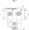
- FIG. 1 is a block diagram illustrating the switching power supply according to the present embodiment.
- the switching power supply illustrated in FIG. 1 is, for example, an apparatus that converts a voltage input from an input terminal I including a first positive terminal T 1 and a first negative terminal T 2 , and outputs the converted voltage from an output terminal O including a second positive terminal T 3 and a second negative terminal T 4 .
- the switching power supply illustrated in FIG. 1 includes a voltage converter 10, a control circuit 20, and a delay circuit 30.
- the voltage converter 10 converts the voltage input from the input terminal I, and outputs the converted voltage from the output terminal O.
- the voltage converter 10 includes a first switching circuit SW1 serving as a trigger for inputting the voltage from the input terminal I and a second switching circuit SW2 serving as a trigger for outputting, after the input voltage is converted, the converted voltage from the output terminal O.
- the control circuit 20 outputs a control signal for selectively sequentially driving the first switching circuit SW1 and the second switching circuit SW2 described above.
- the control circuit 20 outputs a first control signal for turning on the first switching circuit SW1 and a second control signal for turning on the second switching circuit SW2.
- the first control signal and the second control signal which are output from the control circuit 20 are pulse signals that repeat an on-period or an off-period at a certain cycle.
- the control circuit 20 is, for example, a general-use IC.
- the control circuit 20 is connected to an external power supply Vcc.
- the delay circuit 30 delays, based on control signal for driving any one of the first switching circuit SW1 and the second switching circuit SW2, a subsequent driving timing of the other switching circuit that is not driven. For example, the delay circuit 30 delays, based on the first control signal for turning on the first switching circuit SW1, the subsequent timing for turning on the second switching circuit SW2 that is not driven. In addition, the delay circuit 30 delays, based on the second control signal for turning on the second switching circuit SW2, the subsequent timing for turning on the first switching circuit SW1 that is not driven. Accordingly, the delay circuit 30 provides a dead time when both the first switching circuit SW1 and the second switching circuit SW2 are turned off in a process for selectively sequentially driving the first switching circuit and the second switching circuit SW2.
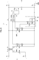
- FIG. 2 is a circuit diagram illustrating an example of the switching power supply illustrated in FIG. 1 .
- the voltage converter 10 illustrated in FIG. 2 includes a transformer Tr.
- the first positive terminal T 1 is connected to one terminal T 5 of a primary winding of the transformer.
- the first negative terminal T 2 is connected to the other terminal T 6 of the primary winding of the transformer Tr.
- the second positive terminal T 3 to one terminal T 7 of a secondary winding of the transformer.
- the second negative terminal T 4 is connected to the other terminal T 8 of the secondary winding of the transformer Tr.
- the second negative terminal T 4 is connected to the ground GND (Ground fault).
- the voltage converter 10 illustrated in FIG. 2 also includes a coil L and a first capacitance C1.
- the coil L is connected between the one terminal T 7 of the secondary winding of the transformer Tr and the second positive terminal T 3 .
- One terminal of the first capacitance C1 is connected between the other terminal of the coil L on the positive terminal side and the second positive terminal T3.
- the other terminal of the first capacitance C1 is connected to the second negative terminal T 4 .
- the other terminal of the first capacitance C1 is connected to the ground GND. That is, the voltage converter 10 illustrated in FIG.
- the second negative terminal T 4 is an insulation type step-down converter in which the transformer Tr is provided between the input terminal I and the output terminal O, and the voltage input from the input terminal I is stepped-down to be output from the output terminal O.
- the transformer Tr is provided between the input terminal I and the output terminal O, and the voltage input from the input terminal I is stepped-down to be output from the output terminal O.
- the input of the voltage to the primary winding side of the transformer Tr is managed by an input side switching circuit Qin.
- a gate of the input side switching circuit Qin is connected to the switching power supply that is not illustrated in the drawing.
- the first switching circuit SW1 is connected between the other terminal T 8 of the secondary winding of the transformer Tr and the second negative terminal T 4 .
- Driving of the first switching circuit SW1 is synchronized with driving of the input side switching circuit Qin. For example, in a case where the input side switching circuit Qin is turned on, the first switching circuit SW1 is turned on.
- One terminal of the second switching circuit SW2 is connected between the one terminal T 7 of the secondary winding of the transformer Tr and one terminal of the coil L on the first positive terminal side.
- the other terminal of the second switching circuit SW2 is connected to the ground GND.
- the first switching circuit SW1 includes a first resistor R1, a second resistor R2, and a first switching element Q1.
- One terminal of the first resistor R1 is connected to a first signal output terminal O 1 configured to output the first control signal (A signal illustrated in FIG. 2 ) in the control circuit 20.
- the second resistor R2 is connected in parallel to the first resistor R1. That is, one terminal of the second resistor R2 is connected to the other terminal of the first resistor R1. In addition, the other terminal of the second resistor R2 is connected to the ground GND.
- the first switching element Q1 is, for example, an n-channel MOS-FET.
- a gate of the first switching element Q1 is connected between the first resistor R1 and the second resistor R2.
- a drain of the first switching element Q1 is connected to the other terminal T 8 of the secondary winding of the transformer Tr.
- a source of the first switching element Q1 is connected to the ground GND.
- the second switching circuit SW2 includes a third resistor R3, a fourth resistor R4, and a second switching element Q2.
- One terminal of the third resistor R3 is connected to a second signal output terminal O 2 configured to output the second control signal (B signal illustrated in FIG. 2 ) in the control circuit 20.
- the fourth resistor R4 is connected in series to the third resistor R3. That is, one terminal of the fourth resistor R4 is connected to the other terminal of the third resistor R3. In addition, the other terminal of the fourth resistor R4 is connected to the ground GND.
- the second switching element Q2 is, for example, an n-channel MOS-FET. A gate of the second switching element Q2 is connected between the third resistor R3 and the fourth resistor R4.
- a drain of the second switching element Q2 is connected between the one terminal T 7 of the secondary winding of the transformer Tr and one terminal of the coil L on the first positive terminal side.
- a source of the second switching element Q2 is connected to the ground GND.
- the delay circuit 30 includes a first delay circuit 31 and a second delay circuit 32.
- the first delay circuit 31 delays, based on the first control signal for turning on the first switching circuit SW1, a subsequent timing for turning on the second switching circuit SW2 that is not driven.
- the first delay circuit 31 includes a fifth resistor R5, a sixth resistor R6, and a third switching element Q3.
- One terminal of the fifth resistor R5 is connected between the first signal output terminal O 1 and the first resistor R1.
- the sixth resistor R6 is connected in series to the fifth resistor R5. That is, one terminal of the sixth resistor R6 is connected to the other terminal of the fifth resistor R5. In addition, the other terminal of the sixth resistor R6 is connected to the ground GND.
- a second capacitance C2 is connected in parallel to the sixth resistor R6. That is, one terminal of the second capacitance C2 is connected between the fifth resistor R5 and the sixth resistor R6 and also connected to a gate of the third switching element Q3. In addition, the other terminal of the second capacitance C2 is connected to the ground GND.
- the gate of the third switching element Q3 is connected between the fifth resistor R5 and the sixth resistor R6.
- a drain of the third switching element Q3 is connected between the third resistor R3 and the fourth resistor R4 and also connected to the gate of the second switching element Q2.
- a source of the third switching element Q3 is connected to the ground GND.
- the second delay circuit 32 delays, based on the second control signal for turning on the second switching circuit SW2, a subsequent timing for turning on the first switching circuit SW1 that is not driven.
- the second delay circuit 32 includes a seventh resistor R7, an eighth resistor R8, and a fourth switching element Q4.
- One terminal of the seventh resistor R7 is connected to the second signal output terminal O 2 .
- the eighth resistor R8 is connected in series to the seventh resistor R7. That is, one terminal of the eighth resistor R8 is connected to the other terminal of the seventh resistor R7.
- the other terminal of the eighth resistor R8 is connected to the ground GND.
- a third capacitance C3 is connected in parallel to the eighth resistor R8.
- the one terminal of the eighth resistor R8 is connected between the seventh resistor R7 and the eighth resistor R8 and also connected to a gate of the fourth switching element Q4.
- the other terminal of the eighth resistor R8 is connected to the ground GND.
- the gate of the fourth switching element Q4 is connected between the seventh resistor R7 and the eighth resistor R8.
- a drain of the fourth switching element Q4 is connected between the first resistor R1 and the first resistor R1 and also connected to the gate of the first switching element Q1.
- a source of the fourth switching element Q4 is connected to the ground GND.
- FIG. 3 is a timing chart in a case where the first control signal and the second control signal are alternately input to the first switching circuit SW1 and the second switching circuit SW2.
- the timing chart illustrated in FIG. 3 indicates a gate-source voltage Vgs and a drain-source voltage Vds in the third switching element Q3, a gate-source voltage Vgs and a drain-source voltage Vds in the fourth switching element Q4, a gate-source voltage Vgs and a drain-source voltage Vds in the first switching element Q1, and a gate-source voltage Vgs and a drain-source voltage Vds in the second switching element Q2 in a case where the first control signal for turning on the first switching circuit SW1 (A signal illustrated in FIG.
- FIG. 3 illustrates the states of the respective elements included in the switching power supply in a case where the A signal and the B signal described above are alternately input.
- the A signal that has passed through the first resistor R1 is input to the gate of the first switching element Q1. Accordingly, the gate-source voltage Vgs in the first switching element Q1 is turned on. In addition, the drain-source voltage Vds in the first switching element Q1 is turned on. That is, the first switching element Q1 is turned on.
- the A signal that has passed through the fifth resistor R5 is input to the second capacitance C2. Accordingly, the second capacitance C2 accumulates charges.
- the A signal that has passed through the fifth resistor R5 is also input to the gate of the third switching element Q3. Accordingly, the gate-source voltage Vgs in the third switching element Q3 is turned on. In addition, the drain-source voltage Vds in the third switching element Q3 is turned on. That is, the third switching element Q3 is turned on.
- the A signal is not input to the gate of the first switching element Q1. Accordingly, the gate-source voltage Vgs in the first switching element Q1 is turned off. In addition, the drain-source voltage Vds in the first switching element Q1 is turned off. That is, the first switching element Q1 is turned off.
- the A signal is not input to the second capacitance C2.
- the second capacitance C2 supplies the accumulated charges to the gate of the third switching element Q3.
- a part of the charges output from the second capacitance C2 is also supplied to the gate of the first switching element Q1 via a supply path of the A signal.
- the fifth resistor R5 and the first resistor R1 exist in the supply path, the voltage is decreased. Accordingly, even when the part of the charges is input to the gate of the first switching element Q1, a gate threshold voltage of the first switching element Q1 does not increase to a predetermined value. That is, the first switching element Q1 is not turned on.
- the A signal is not input to the gate of the third switching element Q3. Accordingly, the gate-source voltage Vgs in the third switching element Q3 is turned off. In addition, the drain-source voltage Vds in the third switching element Q3 is turned off. That is, the third switching element Q3 is turned off. At this time, the third switching element Q3 is turned off later than the first switching element Q1. A reason for this is because the charges are supplied to the gate of the third switching element Q3 from the second capacitance C2. When the charges are supplied from the second capacitance C2, a voltage exceeding a gate threshold voltage of the third switching element Q3 is applied for a predetermined time.
- the predetermined time can be obtained from a pulse width of the B signal supplied to the second capacitance C2 and a time constant calculated from the fifth resistor R5, the sixth resistor R6, and the second capacitance C2.
- the timing at which the third switching element Q3 is turned off is delayed by a predetermined time calculated from the pulse width of the B signal supplied to the second capacitance C2, and the fifth resistor R5, the sixth resistor R6, and the second capacitance C2. After the elapse of the certain time, the third switching element Q3 is turned off.
- the B signal that has passed through the third resistor R3 is input to the gate of the second switching element Q2.
- the second switching element Q2 remains off.
- a reason for this is because the third switching element Q3 is turned off later than the first switching element Q1.
- the third switching element Q3 remains on. In other words, since continuity is provided between the drain and the source of the third switching element Q3, a part of the B signal that has passed through the third resistor R3 flows between the drain and the source of the third switching element Q3.
- a gate threshold voltage of the second switching element Q2 does not increase to a predetermined value. That is, since the third switching element Q3 is turned off later than the first switching element Q1, it is possible to delay the timing for turning on the second switching element Q2. As a result, it is possible to secure the time (dead time) Td when both the first switching element Q1 and the second switching element Q2 are turned off.
- the third switching element Q3 is turned off, and then the gate-source voltage Vgs in the second switching element Q2 is turned on.
- the drain-source voltage Vds in the second switching element Q2 is turned on. That is, the second switching element Q2 is turned on.
- the B signal that has passed through the seventh resistor R7 is input to the third capacitance C3. Accordingly, the third capacitance C3 accumulates charges.
- the B signal that has passed through the seventh resistor R7 is also input to the gate of the fourth switching element Q4. Accordingly, the gate-source voltage Vgs in the fourth switching element Q4 is turned on. In addition, the drain-source voltage Vds in the fourth switching element Q4 is turned on. That is, the fourth switching element Q4 is turned on.
- the B signal is not input to the gate of the second switching element Q2. Accordingly, the gate-source voltage Vgs in the second switching element Q2 is turned off. In addition, the drain-source voltage Vds in the second switching element Q2 is turned off. That is, the second switching element Q2 is turned off.
- the B signal is not input to the third capacitance C3.
- the third capacitance C3 supplies the accumulated charges to the gate of the fourth switching element Q4.
- a part of the charges output from the third capacitance C3 is also supplied to the gate of the second switching element Q2 via the supply path of the B signal.
- the seventh resistor R7 and the third resistor R3 exist in the supply path, the voltage is decreased. Accordingly, even when the part of the charges is input to the gate of the second switching element Q2, the gate threshold voltage of the second switching element Q2 does not increase to the predetermined value. That is, the second switching element Q2 is not turned on.
- the B signal is not input to the gate of the fourth switching element Q4. Accordingly, the gate-source voltage Vgs in the fourth switching element Q4 is turned off. In addition, the drain-source voltage Vds in the fourth switching element Q4 is turned off. That is, the fourth switching element Q4 is turned off. At this time, the fourth switching element Q4 is turned off later than the second switching element Q2. A reason for this is because the charges are supplied to the gate of the fourth switching element Q4 from the third capacitance C3. When the charges are supplied from the third capacitance C3, a voltage exceeding a gate threshold voltage of the fourth switching element Q4 is applied for a predetermined time.
- the predetermined time can be obtained from a pulse width of the A signal supplied to the third capacitance C3 and a time constant calculated from the seventh resistor R7, the eighth resistor R8, and the third capacitance C3.
- the timing at which the fourth switching element Q4 is turned off is delayed by a predetermined time calculated from the pulse width of the A signal supplied to the third capacitance C3, and the seventh resistor R7, the eighth resistor R8, and the third capacitance C3. After the elapse of the certain time, the fourth switching element Q4 is turned off.
- the A signal that has passed through the first resistor R1 is input to the gate of the first switching element Q1.
- the first switching element Q1 remains off.
- the fourth switching element Q4 is turned off later than the second switching element Q2.
- the fourth switching element Q4 remains on. In other words, since continuity is provided between the drain and the source of the fourth switching element Q4, a part of the A signal that has passed through the first resistor R1 flows between the drain and the source of the fourth switching element Q4.
- the gate threshold voltage of the first switching element Q1 does not increase to the predetermined value. That is, since the fourth switching element Q4 is turned off later than the second switching element Q2, it is possible to delay the timing for turning on the first switching element Q1. As a result, it is possible to secure the time (dead time) Td when both the first switching element Q1 and the second switching element Q2 are turned off.
- the fourth switching element Q4 is turned off, and then the gate-source voltage Vgs in the first switching element Q1 is turned on.
- the drain-source voltage Vds in the first switching element Q1 is turned on. That is, the first switching element Q1 is turned on.
- the A signal that has passed through the fifth resistor R5 is input to the second capacitance C2. Accordingly, the second capacitance C2 accumulates charges.
- the A signal that has passed through the fifth resistor R5 is also input to the gate of the third switching element Q3. Accordingly, the gate-source voltage Vgs in the third switching element Q3 is turned on. In addition, the drain-source voltage Vds in the third switching element Q3 is turned on. That is, the third switching element Q3 is turned on.
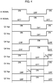
- FIG. 4 is a timing chart in a case where the first control signal and the second control signal are discretely input to the first switching circuit SW1 and the second switching circuit SW2.
- the timing chart illustrated in FIG. 4 indicates the gate-source voltage Vgs and the drain-source voltage Vds in the third switching element Q3, the gate-source voltage Vgs and the drain-source voltage Vds in the fourth switching element Q4, the gate-source voltage Vgs and the drain-source voltage Vds in the first switching element Q1, and the gate-source voltage Vgs and the drain-source voltage Vds in the second switching element Q2 in a case where the first control signal for turning on the first switching circuit SW1 (A signal illustrated in FIG.
- FIG. 4 illustrates the states of the respective elements included in the switching power supply in a case where the A signal and the B signal described above are discretely input.
- the first switching element Q1 is turned on.
- the second capacitance C2 accumulates charges.
- the third switching element Q3 is turned on.
- the first switching element Q1 is turned off.
- the second capacitance C2 supplies the accumulated charges to the gate of the third switching element Q3.
- the third switching element Q3 is turned off later than the first switching element Q1. A reason for this is because the charges are supplied to the gate of the third switching element Q3 from the second capacitance C2. After the elapse of the certain time, the third switching element Q3 is turned off.
- the second switching element Q2 remains off.
- a reason for this is because the third switching element Q3 is turned off later than the first switching element Q1. That is, since the third switching element Q3 is turned off later than the first switching element Q1, it is possible to delay the timing for turning on the second switching element Q2. As a result, it is possible to secure the time (dead time) Td when both the first switching element Q1 and the second switching element Q2 are turned off.
- the third switching element Q3 is turned off, and then the second switching element Q2 is turned on.
- the third capacitance C3 accumulates charges.
- the fourth switching element Q4 is turned on.
- the second switching element Q2 is turned off.
- the third capacitance C3 supplies the accumulated charges to the gate of the fourth switching element Q4.
- the fourth switching element Q4 is turned off later than the second switching element Q2. A reason for this is because the charges are supplied to the gate of the fourth switching element Q4 from the third capacitance C3. After the elapse of the certain time, the fourth switching element Q4 is turned off.
- the first switching element Q1 remains off.
- a reason for this is because the fourth switching element Q4 is turned off later than the second switching element Q2. That is, since the fourth switching element Q4 is turned off later than the second switching element Q2, it is possible to delay the timing for turning on the first switching element Q1. As a result, it is possible to secure the time (dead time) Td when both the first switching element Q1 and the second switching element Q2 are turned off.
- the fourth switching element Q4 is turned off, and then the first switching element Q1 is turned on.
- the second capacitance C2 accumulates charges.
- the third switching element Q3 is turned on.
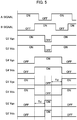
- FIG. 5 is a timing chart in a case where the first control signal and the second control signal are input to the first switching circuit SW1 and the second switching circuit SW2 while being overlapped with each other.
- the timing chart illustrated in FIG. 5 indicates the gate-source voltage Vgs and the drain-source voltage Vds in the third switching element Q3, the gate-source voltage Vgs and the drain-source voltage Vds in the fourth switching element Q4, the gate-source voltage Vgs and the drain-source voltage Vds in the first switching element Q1, and the gate-source voltage Vgs and the drain-source voltage Vds in the second switching element Q2 in a case where the first control signal for turning on the first switching circuit SW1 (A signal illustrated in FIG.
- FIG. 5 illustrates the states of the respective elements included in the switching power supply in a case where the A signal and the B signal described above are input while being overlapped with each other.
- the first switching element Q1 is turned on.
- the second capacitance C2 accumulates charges.
- the third switching element Q3 is turned on.
- the third switching element Q3 is turned on.
- the fourth switching element Q4 is turned on.
- a reason for this is because both the A signal and the B signal are turned on.
- the fourth switching element Q4 is on, even when the A signal is input to the gate of the first switching element Q1, a part of the A signal flows into the fourth switching element Q4. Accordingly, the gate threshold voltage of the first switching element Q1 does not increase to the predetermined value. That is, the first switching element Q1 is turned off.
- the third switching element Q3 is on, even when the B signal is input to the gate of the second switching element Q2, a part of the B signal flows into the third switching element Q3. Accordingly, the gate threshold voltage of the second switching element Q2 does not increase to the predetermined value. That is, the second switching element Q2 is turned off.
- the first switching element Q1 is turned off.
- the second capacitance C2 supplies the accumulated charges to the gate of the third switching element Q3.
- the third switching element Q3 is turned off later than the first switching element Q1. A reason for this is because the charges are supplied to the gate of the third switching element Q3 from the second capacitance C2. After the elapse of the certain time, the third switching element Q3 is turned off.
- the second switching element Q2 remains off.
- a reason for this is because the third switching element Q3 is turned off later than the first switching element Q1. That is, since the third switching element Q3 is turned off later than the first switching element Q1, it is possible to delay the timing for turning on the second switching element Q2. As a result, it is possible to secure the time (dead time) Td when both the first switching element Q1 and the second switching element Q2 are turned off.
- the third switching element Q3 is turned off, and then the second switching element Q2 is turned on.
- the third capacitance C3 accumulates charges.
- the fourth switching element Q4 is turned on.
- the third switching element Q3 is turned on.
- the fourth switching element Q4 is turned on. Since the third switching element Q3 and the fourth switching element Q4 are on, the first switching element Q1 and the second switching element Q2 are turned off.
- the second switching element Q2 is turned off.
- the third capacitance C3 supplies the accumulated charges to the gate of the fourth switching element Q4.
- the fourth switching element Q4 is turned off later than the second switching element Q2. A reason for this is because the charges are supplied to the gate of the fourth switching element Q4 from the third capacitance C3. After the elapse of the certain time, the fourth switching element Q4 is turned off.
- the first switching element Q1 remains off.
- a reason for this is because the fourth switching element Q4 is turned off later than the second switching element Q2. That is, since the fourth switching element Q4 is turned off later than the second switching element Q2, it is possible to delay the timing for turning on the first switching element Q1. As a result, it is possible to secure the time (dead time) Td when both the first switching element Q1 and the second switching element Q2 are turned off.
- the fourth switching element Q4 is turned off, and then the first switching element Q1 is turned on.
- the second capacitance C2 accumulates charges.
- the third switching element Q3 is turned on.
- the first switching element Q1 is turned on.
- the second capacitance C2 accumulates charges.
- the fourth switching element Q4 is turned on.
- the third switching element Q3 is turned on.
- the second capacitance C2 accumulates charges.
- the second switching element Q2 remains off. A reason for this is because the third switching element Q3 is turned on. That is, the second switching element Q2 is turned off.
- the first switching element Q1 is turned off.
- the second capacitance C2 supplies the accumulated charges to the gate of the third switching element Q3.
- the third switching element Q3 is turned off later than the first switching element Q1. A reason for this is because the charges are supplied to the gate of the third switching element Q3 from the second capacitance C2. After the elapse of the certain time, the third switching element Q3 is turned off.
- the second switching element Q2 remains off.
- a reason for this is because the third switching element Q3 is turned off later than the first switching element Q1. That is, since the fourth switching element Q4 is turned off later than the second switching element Q2, it is possible to delay the timing for turning on the first switching element Q1. As a result, it is possible to secure the time (dead time) Td when both the first switching element Q1 and the second switching element Q2 are turned off.
- the third switching element Q3 is turned off, and then the second switching element Q2 is turned on.
- the third capacitance C3 accumulates charges.
- the fourth switching element Q4 is turned on.
- the switching power supply according to the present embodiment provides the dead time when both the first switching element Q1 and the second switching element Q2 are turned off, by the first delay circuit 31 and the second delay circuit 32. Accordingly, it is possible to avoid the state where the first switching element Q1 and the second switching element Q2 are turned on at the same time. In addition, as described above, the dead time is secured even when the first control signal and the second control signal are input at various timings, and it is possible to avoid the state where the first switching element Q1 and the second switching element Q2 are turned on at the same time.
- the switching power supply according to the present embodiment can improve efficiency of step-up and step-down.
- an operation similar to the dedicated-use IC can be performed by a general-use IC.
- the switching power supply according to the above-described embodiment a configuration including the first delay circuit 31 and the second delay circuit 32 is illustrated as an example.
- the switching power supply according to the present embodiment is not limited to this.
- the switching power supply according to the present embodiment may also adopt a configuration where turning-on of only one of the switching circuits can be delayed.
- FIG. 6 is a circuit diagram illustrating an example of the switching power supply according to a modified example.
- FIG. 6 illustrates a circuit diagram in which a time until the second switching circuit SW2 is turned on is delayed.
- a delay circuit 33 includes the first delay circuit 31.
- the first delay circuit 31 delays, based on the first control signal for turning on the first switching circuit SW1, the time until the second switching circuit SW2 is turned on. It is noted that detailed descriptions will be omitted with regard to the parts redundant with those in FIG. 2 described above.
- FIG. 7 is a timing chart in a case where the first control signal and the second control signal are alternately input to the first switching circuit SW1 and the second switching circuit SW2.
- the timing chart illustrated in FIG. 7 indicates the gate-source voltage Vgs and the drain-source voltage Vds in the third switching element Q3, the gate-source voltage Vgs and the drain-source voltage Vds in the first switching element Q1, and the gate-source voltage Vgs and the drain-source voltage Vds in the second switching element Q2 in a case where the first control signal for turning on the first switching circuit SW1 (A signal illustrated in FIG. 7 ) and the second control signal for turning on the second switching circuit SW2 (B signal illustrated in FIG. 7 ) are alternately input by the control circuit 20. That is, FIG. 7 illustrates the states of the respective elements included in the switching power supply in a case where the A signal and the B signal described above are alternately input.
- the first switching element Q1 is turned on.
- the second capacitance C2 accumulates charges.
- the third switching element Q3 is turned on.
- the first switching element Q1 is turned off.
- the second capacitance C2 supplies the accumulated charges to the gate of the third switching element Q3.
- the third switching element Q3 is turned off later than the first switching element Q1. A reason for this is because the charges are supplied to the gate of the third switching element Q3 from the second capacitance C2.
- the second switching element Q2 remains off.
- a reason for this is because the third switching element Q3 is turned off later than the first switching element Q1. That is, since the third switching element Q3 is turned off later than the first switching element Q1, it is possible to delay the timing for turning on the second switching element Q2. As a result, it is possible to secure the time (dead time) Td when both the first switching element Q1 and the second switching element Q2 are turned off. After the elapse of the certain time, the third switching element Q3 is turned off, and then the second switching element Q2 is turned on.
- the second switching element Q2 is turned off.
- FIG. 8 is a timing chart in a case where the first control signal and the second control signal are discretely input to the first switching circuit SW1 and the second switching circuit SW2.
- the timing chart illustrated in FIG. 8 indicates the gate-source voltage Vgs and the drain-source voltage Vds in the third switching element Q3, the gate-source voltage Vgs and the drain-source voltage Vds in the first switching element Q1, and the gate-source voltage Vgs and the drain-source voltage Vds in the second switching element Q2 in a case where the first control signal for turning on the first switching circuit SW1 (A signal illustrated in FIG. 8 ) and the second control signal for turning on the second switching circuit SW2 (B signal illustrated in FIG. 8 ) are discretely input by the control circuit 20. That is, FIG. 8 illustrates the states of the respective elements included in the switching power supply in a case where the A signal and the B signal described above are discretely input.
- the first switching element Q1 is turned on.
- the second capacitance C2 accumulates charges.
- the third switching element Q3 is turned on.
- the first switching element Q1 is turned off.
- the second capacitance C2 supplies the accumulated charges to the gate of the third switching element Q3.
- the third switching element Q3 is turned off later than the first switching element Q1. A reason for this is because the charges are supplied to the gate of the third switching element Q3 from the second capacitance C2. After the elapse of the certain time, the third switching element Q3 is turned off.
- the second switching element Q2 remains off.
- a reason for this is because the third switching element Q3 is turned off later than the first switching element Q1. That is, since the third switching element Q3 is turned off later than the first switching element Q1, it is possible to delay the timing for turning on the second switching element Q2. As a result, it is possible to secure the time (dead time) Td when both the first switching element Q1 and the second switching element Q2 are turned off. After the elapse of the certain time, the third switching element Q3 is turned off, and then the second switching element Q2 is turned on.
- the second switching element Q2 is turned off.
- the switching power supply according to the present embodiment provides the dead time when both the first switching element Q1 and the second switching element Q2 are turned off, by the first delay circuit 31. Accordingly, it is possible to avoid the state where the first switching element Q1 and the second switching element Q2 are turned on at the same time. In addition, as described above, the dead time is secured even when the first control signal and the second control signal are input at various timings, and it is possible to avoid the state where the first switching element Q1 and the second switching element Q2 are turned on at the same time.
- the switching power supply according to the present embodiment can improve the efficiency of step-up and step-down.
- the operation similar to the dedicated-use IC can be performed by the general-use IC.
- the switching power supply includes the input terminal I and the output terminal O, the voltage converter 10 that includes the first switching circuit SW1 configured to serve as a trigger for inputting the voltage from the input terminal I and the second switching circuit SW2 configured to serve as a trigger for outputting, after the input voltage is converted, the converted voltage from the output terminal O, the control circuit 20 configured to output a control signal for selectively sequentially driving the first switching circuit SW1 and the second switching circuit SW2, and the delay circuit configured to delay, based on the control signal for driving any one of the first switching circuit SW1 and the second switching circuit SW2, the subsequent driving timing of the other switching circuit that is not driven to provide the dead time when both the first switching circuit SW1 and the second switching circuit SW2 are turned off.
- the switching power supply according to the present embodiment provides the dead time when both the first switching element Q1 and the second switching element Q2 are turned off, by the delay circuit 30. Accordingly, it is possible to avoid the state where the first switching element Q1 and the second switching element Q2 are turned on at the same time. In addition, as described above, the dead time is secured even when the first control signal and the second control signal are input at various timings, and it is possible to avoid the state where the first switching element Q1 and the second switching element Q2 are turned on at the same time.
- the switching power supply according to the present embodiment can improve the efficiency of step-up and step-down.
- the operation similar to the dedicated-use IC can be performed by the general-use IC.
- the switching power supply according to the present embodiment can improve the efficiency of the step-up and step-down while the risks such as the circuit damage in the voltage step-up and step-down operations are reduced.
- the insulation type step-down converter is illustrated as the voltage converter 10.
- the switching power supply according to the present embodiment is not limited to this.
- the present embodiment can also be applied to a non-insulation type step-down converter, an insulation type step-up converter, a non-insulation type step-up converter, a non-insulation type bidirectional converter, or an insulation type bidirectional converter.
- a switching power supply includes an input terminal and an output terminal, a voltage converter including a first switching circuit configured to serve as a trigger for inputting a voltage from the input terminal and a second switching circuit configured to serve as a trigger for outputting, after the input voltage is converted, the converted voltage from the output terminal, a control circuit configured to output a control signal for selectively sequentially driving the first switching circuit and the second switching circuit, and a delay circuit configured to delay, based on the control signal for driving any one of the first switching circuit and the second switching circuit, a subsequent driving timing of the other switching circuit that is not driven to provide a dead time when both the first switching circuit and the second switching circuit are turned off.
- the switching power supply according to the first mode of the present invention provides the dead time when both the first switching circuit and the second switching circuit are turned off, by the delay circuit. Accordingly, it is possible to avoid the state where the first switching circuit and the second switching circuit are turned on at the same time. In addition, the dead time is secured even when the first control signal and the second control signal are input at various timings, and it is possible to avoid the state where the first switching circuit and the second switching circuit are turned on at the same time.
- the switching power supply according to the first mode of the present invention can improve the efficiency of the step-up and step-down while the risks such as the circuit damage in the voltage step-up and step-down operations are reduced.
- a delay circuit in a switching power supply according to a second mode of the present invention includes, in the switching power supply according to the above-described first mode, a first resistor connected to a signal output terminal for outputting the control signal to the driven switching circuit in the control circuit, a second resistor connected in series to the first resistor, a capacitance connected in parallel to the second resistor, and a switching element having a gate connected between the first resistor and the second resistor and a drain connected to the other switching circuit that is not driven.
- the switching power supply according to the second mode of the present invention can adjust the dead time to the optimal time appropriate to the circuit by adjusting the values of the first resistor, the second resistor, and the capacitance which are included in the delay circuit. Accordingly, the switching power supply according to the second mode of the present invention can improve the efficiency of step-up and step-down.
- the switching power supply according to the second mode of the present invention can improve the efficiency of the step-up and step-down while the risks such as the circuit damage in the voltage step-up and step-down operations are reduced.
Landscapes
- Engineering & Computer Science (AREA)
- Power Engineering (AREA)
- Dc-Dc Converters (AREA)
- Power Conversion In General (AREA)
- Rectifiers (AREA)
- Electronic Switches (AREA)
Abstract
Description
- The present invention relates to a switching power supply that converts and outputs an input voltage.
- A switching power supply includes an input terminal and an output terminal, converts a voltage input from the input terminal and outputs the converted voltage to the output terminal. In the switching power supply, a first transistor serving as a trigger for inputting the voltage from the input terminal and a second transistor serving as a trigger for outputting the voltage from the output terminal are turned on and off by an control signal output from a dedicated-use IC, so that the voltage input from the input terminal is output from the output terminal. The above-described switching power supply is configured to provide a time (dead time) when both the first transistor and the second transistor are turned off, and set a configuration where both the first transistor and the second transistor are not turned on at the same time. The dead time is fixed by the dedicated-use IC.
- Patent Document 1: Japanese Patent Laid-Open No.
2001-112241 - On the other hand, since on and off of a first transistor and a second transistor are controlled by a dedicated-use IC, a highly versatile IC is not to be used. In addition, since a dead time is fixed by the dedicated-use IC, there is a possibility that the first transistor and the second transistor may be turned on at the same time depending on a configuration of the circuit. When the first transistor and the second transistor are turned on at the same time, the circuit is damaged. Furthermore, since the dead time is fixed by the dedicated-use IC, an adjustment to set any dead time is not to be performed. Accordingly, since an adjustment to a dead time optimal to the circuit is not performed, efficiency of step-up and step-down in a switching power supply is not improved.
- The present invention has been made in view of the above-described circumstances, and is aimed at providing a switching power supply that can improve efficiency of step-up and step-down while risks such as circuit damage in voltage step-up and step-down operations are reduced.
- In order to achieve the above object, an aspect of the present invention is directed to a switching power supply including an input terminal and an output terminal, a voltage converter including a first switching circuit configured to serve as a trigger for inputting a voltage from the input terminal and a second switching circuit configured to serve as a trigger for outputting, after the input voltage is converted, the converted voltage from the output terminal, a control circuit configured to output a control signal for selectively sequentially driving the first switching circuit and the second switching circuit, and a delay circuit configured to delay, based on the control signal for driving any one of the first switching circuit and the second switching circuit, a subsequent driving timing of the other switching circuit that is not driven to provide a dead time when both the first switching circuit and the second switching circuit are turned off.
- In accordance with the above-described configuration, in the switching power supply according to the aspect of the present invention, the dead time when both the first switching circuit and the second switching circuit are turned off is provided by the delay circuit. Accordingly, it is possible to avoid a state where the first switching circuit and the second switching circuit are turned on at the same time. In addition, the dead time is secured even when a first control signal and a second control signal are input at various timings, and it is possible to avoid a state where the first switching circuit and the second switching circuit are turned on at the same time.
- The switching power supply according to the aspect of the present invention can improve the efficiency of the step-up and step-down while the risks such as the circuit damage in the voltage step-up and step-down operations are reduced.
- The present invention will become more fully understood from the detailed description given hereinafter and the accompanying drawings which are given by way of illustration only, and thus, are not limitative of the present invention, and characterized in that:
-
FIG. 1 is a block diagram illustrating a switching power supply according to a present embodiment. -
FIG. 2 is a circuit diagram illustrating an example of the switching power supply illustrated inFIG. 1 . -
FIG. 3 is a timing chart in a case where a first control signal and a second control signal are alternately input to a first switching circuit and a second switching circuit. -
FIG. 4 is a timing chart in a case where the first control signal and the second control signal are discretely input to the first switching circuit and the second switching circuit. -
FIG. 5 is a timing chart in a case where the first control signal and the second control signal are input while being overlapped with each other to the first switching circuit and the second switching circuit. -
FIG. 6 is a circuit diagram illustrating an example of the switching power supply according to a modified example. -
FIG. 7 is a timing chart in the modified example in a case where the first control signal and the second control signal are alternately input to the first switching circuit and the second switching circuit. -
FIG. 8 is a timing chart in the modified example in a case where the first control signal and the second control signal are discretely input to the first switching circuit and the second switching circuit. - Hereinafter, a switching power supply according to one present embodiment of the present invention will be described with reference to the drawings. It is noted that the present embodiment is not limited by contents which will be described below, and can be implemented by optionally making a change within a range without departing from the gist thereof. In addition, each of the drawings used for describing the embodiment schematically illustrates a component, in which partial emphasis, expansion, reduction, omission, or the like is performed to improve understanding, and in some cases, the drawing does not accurately represent a scale, a shape, or the like of the component.
-
FIG. 1 is a block diagram illustrating the switching power supply according to the present embodiment. The switching power supply illustrated inFIG. 1 is, for example, an apparatus that converts a voltage input from an input terminal I including a first positive terminal T1 and a first negative terminal T2, and outputs the converted voltage from an output terminal O including a second positive terminal T3 and a second negative terminal T4. The switching power supply illustrated inFIG. 1 includes avoltage converter 10, acontrol circuit 20, and adelay circuit 30. - The
voltage converter 10 converts the voltage input from the input terminal I, and outputs the converted voltage from the output terminal O. Thevoltage converter 10 includes a first switching circuit SW1 serving as a trigger for inputting the voltage from the input terminal I and a second switching circuit SW2 serving as a trigger for outputting, after the input voltage is converted, the converted voltage from the output terminal O. - The
control circuit 20 outputs a control signal for selectively sequentially driving the first switching circuit SW1 and the second switching circuit SW2 described above. For example, thecontrol circuit 20 outputs a first control signal for turning on the first switching circuit SW1 and a second control signal for turning on the second switching circuit SW2. The first control signal and the second control signal which are output from thecontrol circuit 20 are pulse signals that repeat an on-period or an off-period at a certain cycle. Thecontrol circuit 20 is, for example, a general-use IC. Thecontrol circuit 20 is connected to an external power supply Vcc. - The
delay circuit 30 delays, based on control signal for driving any one of the first switching circuit SW1 and the second switching circuit SW2, a subsequent driving timing of the other switching circuit that is not driven. For example, thedelay circuit 30 delays, based on the first control signal for turning on the first switching circuit SW1, the subsequent timing for turning on the second switching circuit SW2 that is not driven. In addition, thedelay circuit 30 delays, based on the second control signal for turning on the second switching circuit SW2, the subsequent timing for turning on the first switching circuit SW1 that is not driven. Accordingly, thedelay circuit 30 provides a dead time when both the first switching circuit SW1 and the second switching circuit SW2 are turned off in a process for selectively sequentially driving the first switching circuit and the second switching circuit SW2. - Furthermore, a detailed circuit configuration of each unit illustrated in
FIG. 1 will be described with reference toFIG. 2. FIG. 2 is a circuit diagram illustrating an example of the switching power supply illustrated inFIG. 1 . Herein, thevoltage converter 10 illustrated inFIG. 2 includes a transformer Tr. As illustrated inFIG. 2 , the first positive terminal T1 is connected to one terminal T5 of a primary winding of the transformer. The first negative terminal T2 is connected to the other terminal T6 of the primary winding of the transformer Tr. The second positive terminal T3 to one terminal T7 of a secondary winding of the transformer. The second negative terminal T4 is connected to the other terminal T8 of the secondary winding of the transformer Tr. The second negative terminal T4 is connected to the ground GND (Ground fault). - The
voltage converter 10 illustrated inFIG. 2 also includes a coil L and a first capacitance C1. The coil L is connected between the one terminal T7 of the secondary winding of the transformer Tr and the second positive terminal T3. One terminal of the first capacitance C1 is connected between the other terminal of the coil L on the positive terminal side and the second positive terminal T3. In addition, the other terminal of the first capacitance C1 is connected to the second negative terminal T4. In other words, the other terminal of the first capacitance C1 is connected to the ground GND. That is, thevoltage converter 10 illustrated inFIG. 2 is an insulation type step-down converter in which the transformer Tr is provided between the input terminal I and the output terminal O, and the voltage input from the input terminal I is stepped-down to be output from the output terminal O. Hereinafter, in the embodiment, for convenience of the descriptions, a case of the connection to the second negative terminal T4 will be described as being connected to the ground GND. - In addition, the input of the voltage to the primary winding side of the transformer Tr is managed by an input side switching circuit Qin. A gate of the input side switching circuit Qin is connected to the switching power supply that is not illustrated in the drawing.
- The first switching circuit SW1 is connected between the other terminal T8 of the secondary winding of the transformer Tr and the second negative terminal T4. Driving of the first switching circuit SW1 is synchronized with driving of the input side switching circuit Qin. For example, in a case where the input side switching circuit Qin is turned on, the first switching circuit SW1 is turned on. One terminal of the second switching circuit SW2 is connected between the one terminal T7 of the secondary winding of the transformer Tr and one terminal of the coil L on the first positive terminal side. In addition, the other terminal of the second switching circuit SW2 is connected to the ground GND.
- Herein, a circuit configuration of the first switching circuit SW1 and the second switching circuit SW2 will be described in detail. The first switching circuit SW1 includes a first resistor R1, a second resistor R2, and a first switching element Q1. One terminal of the first resistor R1 is connected to a first signal output terminal O1 configured to output the first control signal (A signal illustrated in
FIG. 2 ) in thecontrol circuit 20. The second resistor R2 is connected in parallel to the first resistor R1. That is, one terminal of the second resistor R2 is connected to the other terminal of the first resistor R1. In addition, the other terminal of the second resistor R2 is connected to the ground GND. The first switching element Q1 is, for example, an n-channel MOS-FET. A gate of the first switching element Q1 is connected between the first resistor R1 and the second resistor R2. In addition, a drain of the first switching element Q1 is connected to the other terminal T8 of the secondary winding of the transformer Tr. In addition, a source of the first switching element Q1 is connected to the ground GND. - The second switching circuit SW2 includes a third resistor R3, a fourth resistor R4, and a second switching element Q2. One terminal of the third resistor R3 is connected to a second signal output terminal O2 configured to output the second control signal (B signal illustrated in
FIG. 2 ) in thecontrol circuit 20. The fourth resistor R4 is connected in series to the third resistor R3. That is, one terminal of the fourth resistor R4 is connected to the other terminal of the third resistor R3. In addition, the other terminal of the fourth resistor R4 is connected to the ground GND. The second switching element Q2 is, for example, an n-channel MOS-FET. A gate of the second switching element Q2 is connected between the third resistor R3 and the fourth resistor R4. In addition, a drain of the second switching element Q2 is connected between the one terminal T7 of the secondary winding of the transformer Tr and one terminal of the coil L on the first positive terminal side. In addition, a source of the second switching element Q2 is connected to the ground GND. - The
delay circuit 30 includes afirst delay circuit 31 and asecond delay circuit 32. Thefirst delay circuit 31 delays, based on the first control signal for turning on the first switching circuit SW1, a subsequent timing for turning on the second switching circuit SW2 that is not driven. Thefirst delay circuit 31 includes a fifth resistor R5, a sixth resistor R6, and a third switching element Q3. One terminal of the fifth resistor R5 is connected between the first signal output terminal O1 and the first resistor R1. The sixth resistor R6 is connected in series to the fifth resistor R5. That is, one terminal of the sixth resistor R6 is connected to the other terminal of the fifth resistor R5. In addition, the other terminal of the sixth resistor R6 is connected to the ground GND. A second capacitance C2 is connected in parallel to the sixth resistor R6. That is, one terminal of the second capacitance C2 is connected between the fifth resistor R5 and the sixth resistor R6 and also connected to a gate of the third switching element Q3. In addition, the other terminal of the second capacitance C2 is connected to the ground GND. The gate of the third switching element Q3 is connected between the fifth resistor R5 and the sixth resistor R6. In addition, a drain of the third switching element Q3 is connected between the third resistor R3 and the fourth resistor R4 and also connected to the gate of the second switching element Q2. In addition, a source of the third switching element Q3 is connected to the ground GND. - The
second delay circuit 32 delays, based on the second control signal for turning on the second switching circuit SW2, a subsequent timing for turning on the first switching circuit SW1 that is not driven. Thesecond delay circuit 32 includes a seventh resistor R7, an eighth resistor R8, and a fourth switching element Q4. One terminal of the seventh resistor R7 is connected to the second signal output terminal O2. The eighth resistor R8 is connected in series to the seventh resistor R7. That is, one terminal of the eighth resistor R8 is connected to the other terminal of the seventh resistor R7. The other terminal of the eighth resistor R8 is connected to the ground GND. A third capacitance C3 is connected in parallel to the eighth resistor R8. That is, the one terminal of the eighth resistor R8 is connected between the seventh resistor R7 and the eighth resistor R8 and also connected to a gate of the fourth switching element Q4. In addition, the other terminal of the eighth resistor R8 is connected to the ground GND. The gate of the fourth switching element Q4 is connected between the seventh resistor R7 and the eighth resistor R8. In addition, a drain of the fourth switching element Q4 is connected between the first resistor R1 and the first resistor R1 and also connected to the gate of the first switching element Q1. In addition, a source of the fourth switching element Q4 is connected to the ground GND. - Herein, states of respective elements along with on and off of the first switching circuit SW1 and the second switching circuit SW2 in the present embodiment will be described with reference to a timing chart related to on and off of the first switching circuit SW1 and the second switching circuit SW2. It is noted that, in the present embodiment, a case where the first control signal and the second control signal are alternately input, a case where the first control signal and the second control signal are discretely input, and a case where the first control signal and the second control signal are input while being overlapped with each other will be separately described. In addition, in the following embodiment, redundant descriptions are omitted where appropriate.
-
FIG. 3 is a timing chart in a case where the first control signal and the second control signal are alternately input to the first switching circuit SW1 and the second switching circuit SW2. The timing chart illustrated inFIG. 3 indicates a gate-source voltage Vgs and a drain-source voltage Vds in the third switching element Q3, a gate-source voltage Vgs and a drain-source voltage Vds in the fourth switching element Q4, a gate-source voltage Vgs and a drain-source voltage Vds in the first switching element Q1, and a gate-source voltage Vgs and a drain-source voltage Vds in the second switching element Q2 in a case where the first control signal for turning on the first switching circuit SW1 (A signal illustrated inFIG. 3 ) and the second control signal for turning on the second switching circuit SW2 (B signal illustrated inFIG. 3 ) are alternately input by thecontrol circuit 20. That is,FIG. 3 illustrates the states of the respective elements included in the switching power supply in a case where the A signal and the B signal described above are alternately input. - First, in a period from when the A signal illustrated in
FIG. 3 is turned on to a moment immediately before the A signal is turned off, the A signal that has passed through the first resistor R1 is input to the gate of the first switching element Q1. Accordingly, the gate-source voltage Vgs in the first switching element Q1 is turned on. In addition, the drain-source voltage Vds in the first switching element Q1 is turned on. That is, the first switching element Q1 is turned on. - In addition, the A signal that has passed through the fifth resistor R5 is input to the second capacitance C2. Accordingly, the second capacitance C2 accumulates charges. On the other hand, the A signal that has passed through the fifth resistor R5 is also input to the gate of the third switching element Q3. Accordingly, the gate-source voltage Vgs in the third switching element Q3 is turned on. In addition, the drain-source voltage Vds in the third switching element Q3 is turned on. That is, the third switching element Q3 is turned on.
- Next, in a period from when the A signal is turned off to a moment immediately before the B signal is turned on, the A signal is not input to the gate of the first switching element Q1. Accordingly, the gate-source voltage Vgs in the first switching element Q1 is turned off. In addition, the drain-source voltage Vds in the first switching element Q1 is turned off. That is, the first switching element Q1 is turned off.
- In addition, the A signal is not input to the second capacitance C2. The second capacitance C2 supplies the accumulated charges to the gate of the third switching element Q3. Herein, a part of the charges output from the second capacitance C2 is also supplied to the gate of the first switching element Q1 via a supply path of the A signal. However, since the fifth resistor R5 and the first resistor R1 exist in the supply path, the voltage is decreased. Accordingly, even when the part of the charges is input to the gate of the first switching element Q1, a gate threshold voltage of the first switching element Q1 does not increase to a predetermined value. That is, the first switching element Q1 is not turned on.
- In addition, the A signal is not input to the gate of the third switching element Q3. Accordingly, the gate-source voltage Vgs in the third switching element Q3 is turned off. In addition, the drain-source voltage Vds in the third switching element Q3 is turned off. That is, the third switching element Q3 is turned off. At this time, the third switching element Q3 is turned off later than the first switching element Q1. A reason for this is because the charges are supplied to the gate of the third switching element Q3 from the second capacitance C2. When the charges are supplied from the second capacitance C2, a voltage exceeding a gate threshold voltage of the third switching element Q3 is applied for a predetermined time. Herein, the predetermined time can be obtained from a pulse width of the B signal supplied to the second capacitance C2 and a time constant calculated from the fifth resistor R5, the sixth resistor R6, and the second capacitance C2. In the present embodiment, the timing at which the third switching element Q3 is turned off is delayed by a predetermined time calculated from the pulse width of the B signal supplied to the second capacitance C2, and the fifth resistor R5, the sixth resistor R6, and the second capacitance C2. After the elapse of the certain time, the third switching element Q3 is turned off.
- Next, in a period from when the B signal is turned on to a moment immediately before the B signal is turned off, the B signal that has passed through the third resistor R3 is input to the gate of the second switching element Q2. At this time, the second switching element Q2 remains off. A reason for this is because the third switching element Q3 is turned off later than the first switching element Q1. First, since the charges are supplied from the second capacitance C2, the third switching element Q3 remains on. In other words, since continuity is provided between the drain and the source of the third switching element Q3, a part of the B signal that has passed through the third resistor R3 flows between the drain and the source of the third switching element Q3. Accordingly, even when the B signal is input to the gate of the second switching element Q2, a gate threshold voltage of the second switching element Q2 does not increase to a predetermined value. That is, since the third switching element Q3 is turned off later than the first switching element Q1, it is possible to delay the timing for turning on the second switching element Q2. As a result, it is possible to secure the time (dead time) Td when both the first switching element Q1 and the second switching element Q2 are turned off.
- After the elapse of the certain time, the third switching element Q3 is turned off, and then the gate-source voltage Vgs in the second switching element Q2 is turned on. In addition, the drain-source voltage Vds in the second switching element Q2 is turned on. That is, the second switching element Q2 is turned on.
- In addition, the B signal that has passed through the seventh resistor R7 is input to the third capacitance C3. Accordingly, the third capacitance C3 accumulates charges. On the other hand, the B signal that has passed through the seventh resistor R7 is also input to the gate of the fourth switching element Q4. Accordingly, the gate-source voltage Vgs in the fourth switching element Q4 is turned on. In addition, the drain-source voltage Vds in the fourth switching element Q4 is turned on. That is, the fourth switching element Q4 is turned on.
- Next, in a period from when the B signal is turned off to a moment immediately before the A signal is turned on, the B signal is not input to the gate of the second switching element Q2. Accordingly, the gate-source voltage Vgs in the second switching element Q2 is turned off. In addition, the drain-source voltage Vds in the second switching element Q2 is turned off. That is, the second switching element Q2 is turned off.
- In addition, the B signal is not input to the third capacitance C3. The third capacitance C3 supplies the accumulated charges to the gate of the fourth switching element Q4. Herein, a part of the charges output from the third capacitance C3 is also supplied to the gate of the second switching element Q2 via the supply path of the B signal. However, since the seventh resistor R7 and the third resistor R3 exist in the supply path, the voltage is decreased. Accordingly, even when the part of the charges is input to the gate of the second switching element Q2, the gate threshold voltage of the second switching element Q2 does not increase to the predetermined value. That is, the second switching element Q2 is not turned on.
- In addition, the B signal is not input to the gate of the fourth switching element Q4. Accordingly, the gate-source voltage Vgs in the fourth switching element Q4 is turned off. In addition, the drain-source voltage Vds in the fourth switching element Q4 is turned off. That is, the fourth switching element Q4 is turned off. At this time, the fourth switching element Q4 is turned off later than the second switching element Q2. A reason for this is because the charges are supplied to the gate of the fourth switching element Q4 from the third capacitance C3. When the charges are supplied from the third capacitance C3, a voltage exceeding a gate threshold voltage of the fourth switching element Q4 is applied for a predetermined time. Herein, the predetermined time can be obtained from a pulse width of the A signal supplied to the third capacitance C3 and a time constant calculated from the seventh resistor R7, the eighth resistor R8, and the third capacitance C3. In the present embodiment, the timing at which the fourth switching element Q4 is turned off is delayed by a predetermined time calculated from the pulse width of the A signal supplied to the third capacitance C3, and the seventh resistor R7, the eighth resistor R8, and the third capacitance C3. After the elapse of the certain time, the fourth switching element Q4 is turned off.
- Next, in a period from when the A signal is turned on to a moment immediately before the A signal is turned off, the A signal that has passed through the first resistor R1 is input to the gate of the first switching element Q1. At this time, the first switching element Q1 remains off. A reason for this is because the fourth switching element Q4 is turned off later than the second switching element Q2. First, since the charges are supplied from the third capacitance C3, the fourth switching element Q4 remains on. In other words, since continuity is provided between the drain and the source of the fourth switching element Q4, a part of the A signal that has passed through the first resistor R1 flows between the drain and the source of the fourth switching element Q4. Accordingly, even when the A signal is input to the gate of the first switching element Q1, the gate threshold voltage of the first switching element Q1 does not increase to the predetermined value. That is, since the fourth switching element Q4 is turned off later than the second switching element Q2, it is possible to delay the timing for turning on the first switching element Q1. As a result, it is possible to secure the time (dead time) Td when both the first switching element Q1 and the second switching element Q2 are turned off.
- After the elapse of the certain time, the fourth switching element Q4 is turned off, and then the gate-source voltage Vgs in the first switching element Q1 is turned on. In addition, the drain-source voltage Vds in the first switching element Q1 is turned on. That is, the first switching element Q1 is turned on.
- In addition, the A signal that has passed through the fifth resistor R5 is input to the second capacitance C2. Accordingly, the second capacitance C2 accumulates charges. On the other hand, the A signal that has passed through the fifth resistor R5 is also input to the gate of the third switching element Q3. Accordingly, the gate-source voltage Vgs in the third switching element Q3 is turned on. In addition, the drain-source voltage Vds in the third switching element Q3 is turned on. That is, the third switching element Q3 is turned on.
- Thereafter, in a case where the first control signal and the second control signal are alternately input, until the supply of the A signal and the B signal from the
control circuit 20 is ended, the operations in the above-described second period to the fifth period are repeated. -
FIG. 4 is a timing chart in a case where the first control signal and the second control signal are discretely input to the first switching circuit SW1 and the second switching circuit SW2. The timing chart illustrated inFIG. 4 indicates the gate-source voltage Vgs and the drain-source voltage Vds in the third switching element Q3, the gate-source voltage Vgs and the drain-source voltage Vds in the fourth switching element Q4, the gate-source voltage Vgs and the drain-source voltage Vds in the first switching element Q1, and the gate-source voltage Vgs and the drain-source voltage Vds in the second switching element Q2 in a case where the first control signal for turning on the first switching circuit SW1 (A signal illustrated inFIG. 4 ) and the second control signal for turning on the second switching circuit SW2 (B signal illustrated inFIG. 4 ) are discretely input by thecontrol circuit 20. That is,FIG. 4 illustrates the states of the respective elements included in the switching power supply in a case where the A signal and the B signal described above are discretely input. - First, in a period from when the A signal illustrated in
FIG. 4 is turned on to a moment immediately before the A signal is turned off, the first switching element Q1 is turned on. In addition, the second capacitance C2 accumulates charges. In addition, the third switching element Q3 is turned on. - Next, in a period from when the A signal is turned off to a moment immediately before the B signal is turned on, the first switching element Q1 is turned off. In addition, the second capacitance C2 supplies the accumulated charges to the gate of the third switching element Q3. In addition, the third switching element Q3 is turned off later than the first switching element Q1. A reason for this is because the charges are supplied to the gate of the third switching element Q3 from the second capacitance C2. After the elapse of the certain time, the third switching element Q3 is turned off.
- Next, in a period from when the B signal is turned on to a moment immediately before the B signal is turned off, the second switching element Q2 remains off. A reason for this is because the third switching element Q3 is turned off later than the first switching element Q1. That is, since the third switching element Q3 is turned off later than the first switching element Q1, it is possible to delay the timing for turning on the second switching element Q2. As a result, it is possible to secure the time (dead time) Td when both the first switching element Q1 and the second switching element Q2 are turned off.
- After the elapse of the certain time, the third switching element Q3 is turned off, and then the second switching element Q2 is turned on. In addition, the third capacitance C3 accumulates charges. In addition, the fourth switching element Q4 is turned on.
- Next, in a period from when the B signal is turned off to a moment immediately before the A signal is turned on, the second switching element Q2 is turned off. In addition, the third capacitance C3 supplies the accumulated charges to the gate of the fourth switching element Q4. In addition, the fourth switching element Q4 is turned off later than the second switching element Q2. A reason for this is because the charges are supplied to the gate of the fourth switching element Q4 from the third capacitance C3. After the elapse of the certain time, the fourth switching element Q4 is turned off.
- Next, in a period from when the A signal is turned on to a moment immediately before the A signal is turned off, the first switching element Q1 remains off. A reason for this is because the fourth switching element Q4 is turned off later than the second switching element Q2. That is, since the fourth switching element Q4 is turned off later than the second switching element Q2, it is possible to delay the timing for turning on the first switching element Q1. As a result, it is possible to secure the time (dead time) Td when both the first switching element Q1 and the second switching element Q2 are turned off.
- After the elapse of the certain time, the fourth switching element Q4 is turned off, and then the first switching element Q1 is turned on. In addition, the second capacitance C2 accumulates charges. In addition, the third switching element Q3 is turned on.
- Thereafter, in a case where the first control signal and the second control signal are discretely input, until the supply of the A signal and the B signal from the
control circuit 20 is ended, the operations in the above-described second period to the fifth period are repeated. -
FIG. 5 is a timing chart in a case where the first control signal and the second control signal are input to the first switching circuit SW1 and the second switching circuit SW2 while being overlapped with each other. The timing chart illustrated inFIG. 5 indicates the gate-source voltage Vgs and the drain-source voltage Vds in the third switching element Q3, the gate-source voltage Vgs and the drain-source voltage Vds in the fourth switching element Q4, the gate-source voltage Vgs and the drain-source voltage Vds in the first switching element Q1, and the gate-source voltage Vgs and the drain-source voltage Vds in the second switching element Q2 in a case where the first control signal for turning on the first switching circuit SW1 (A signal illustrated inFIG. 5 ) and the second control signal for turning on the second switching circuit SW2 (B signal illustrated inFIG. 5 ) are input by thecontrol circuit 20 while being overlapped with each other due to factors such as a circuit design of thecontrol circuit 20 and erroneous operations of apparatuses. That is,FIG. 5 illustrates the states of the respective elements included in the switching power supply in a case where the A signal and the B signal described above are input while being overlapped with each other. - First, in a period from when the A signal illustrated in
FIG. 5 is turned on to a moment immediately before the B signal is turned on, the first switching element Q1 is turned on. In addition, the second capacitance C2 accumulates charges. In addition, the third switching element Q3 is turned on. - Next, in a period from when the B signal is turned on to a moment immediately before the A signal is turned off, the third switching element Q3 is turned on. In addition, the fourth switching element Q4 is turned on. A reason for this is because both the A signal and the B signal are turned on. On the other hand, since the fourth switching element Q4 is on, even when the A signal is input to the gate of the first switching element Q1, a part of the A signal flows into the fourth switching element Q4. Accordingly, the gate threshold voltage of the first switching element Q1 does not increase to the predetermined value. That is, the first switching element Q1 is turned off. In addition, since the third switching element Q3 is on, even when the B signal is input to the gate of the second switching element Q2, a part of the B signal flows into the third switching element Q3. Accordingly, the gate threshold voltage of the second switching element Q2 does not increase to the predetermined value. That is, the second switching element Q2 is turned off.
- Next, in a period from when the A signal is turned off to a moment immediately before the A signal is turned on, the first switching element Q1 is turned off. In addition, the second capacitance C2 supplies the accumulated charges to the gate of the third switching element Q3. In addition, the third switching element Q3 is turned off later than the first switching element Q1. A reason for this is because the charges are supplied to the gate of the third switching element Q3 from the second capacitance C2. After the elapse of the certain time, the third switching element Q3 is turned off.
- In addition, the second switching element Q2 remains off. A reason for this is because the third switching element Q3 is turned off later than the first switching element Q1. That is, since the third switching element Q3 is turned off later than the first switching element Q1, it is possible to delay the timing for turning on the second switching element Q2. As a result, it is possible to secure the time (dead time) Td when both the first switching element Q1 and the second switching element Q2 are turned off.
- After the elapse of the certain time, the third switching element Q3 is turned off, and then the second switching element Q2 is turned on. In addition, the third capacitance C3 accumulates charges. In addition, the fourth switching element Q4 is turned on.
- Next, similarly as in a period from when the A signal is turned on to a moment immediately before the B signal is turned off, the third switching element Q3 is turned on. In addition, the fourth switching element Q4 is turned on. Since the third switching element Q3 and the fourth switching element Q4 are on, the first switching element Q1 and the second switching element Q2 are turned off.
- Next, in a period from when the B signal is turned off to a moment immediately before the B signal is turned on, the second switching element Q2 is turned off. In addition, the third capacitance C3 supplies the accumulated charges to the gate of the fourth switching element Q4. In addition, the fourth switching element Q4 is turned off later than the second switching element Q2. A reason for this is because the charges are supplied to the gate of the fourth switching element Q4 from the third capacitance C3. After the elapse of the certain time, the fourth switching element Q4 is turned off.
- In addition, the first switching element Q1 remains off. A reason for this is because the fourth switching element Q4 is turned off later than the second switching element Q2. That is, since the fourth switching element Q4 is turned off later than the second switching element Q2, it is possible to delay the timing for turning on the first switching element Q1. As a result, it is possible to secure the time (dead time) Td when both the first switching element Q1 and the second switching element Q2 are turned off.
- After the elapse of the certain time, the fourth switching element Q4 is turned off, and then the first switching element Q1 is turned on. In addition, the second capacitance C2 accumulates charges. In addition, the third switching element Q3 is turned on.
- Next, in a period from when the B signal is turned on to a moment immediately before the A signal is turned off, the first switching element Q1 is turned on. In addition, the second capacitance C2 accumulates charges. In addition, the fourth switching element Q4 is turned on. In addition, the third switching element Q3 is turned on. In addition, the second capacitance C2 accumulates charges.
- In addition, the second switching element Q2 remains off. A reason for this is because the third switching element Q3 is turned on. That is, the second switching element Q2 is turned off.
- Next, in a period from when the A signal is turned off to a moment immediately before the A signal is turned on, the first switching element Q1 is turned off. In addition, the second capacitance C2 supplies the accumulated charges to the gate of the third switching element Q3. In addition, the third switching element Q3 is turned off later than the first switching element Q1. A reason for this is because the charges are supplied to the gate of the third switching element Q3 from the second capacitance C2. After the elapse of the certain time, the third switching element Q3 is turned off.
- In addition, the second switching element Q2 remains off. A reason for this is because the third switching element Q3 is turned off later than the first switching element Q1. That is, since the fourth switching element Q4 is turned off later than the second switching element Q2, it is possible to delay the timing for turning on the first switching element Q1. As a result, it is possible to secure the time (dead time) Td when both the first switching element Q1 and the second switching element Q2 are turned off.
- After the elapse of the certain time, the third switching element Q3 is turned off, and then the second switching element Q2 is turned on. In addition, the third capacitance C3 accumulates charges. In addition, the fourth switching element Q4 is turned on.
- Thereafter, in a case where the first control signal and the second control signal are input while being overlapped with each other, until the supply of the A signal and the B signal from the
control circuit 20 is ended, the operations in the above-described second period to the seventh period are repeated. - In accordance with the above-described configuration, the switching power supply according to the present embodiment provides the dead time when both the first switching element Q1 and the second switching element Q2 are turned off, by the
first delay circuit 31 and thesecond delay circuit 32. Accordingly, it is possible to avoid the state where the first switching element Q1 and the second switching element Q2 are turned on at the same time. In addition, as described above, the dead time is secured even when the first control signal and the second control signal are input at various timings, and it is possible to avoid the state where the first switching element Q1 and the second switching element Q2 are turned on at the same time. - In addition, by adjusting the values of the fifth resistor R5, the sixth resistor R6, and the second capacitance C2 which are included in the
first delay circuit 31 and the seventh resistor R7, the eighth resistor R8, and the third capacitance C3 which are included in thesecond delay circuit 32, it is possible to adjust the dead time to the optimal time appropriate to the circuit. Accordingly, the switching power supply according to the present embodiment can improve efficiency of step-up and step-down. In addition, even when a dedicated-use IC is not used, an operation similar to the dedicated-use IC can be performed by a general-use IC. - In the switching power supply according to the above-described embodiment, a configuration including the
first delay circuit 31 and thesecond delay circuit 32 is illustrated as an example. However, the switching power supply according to the present embodiment is not limited to this. For example, the switching power supply according to the present embodiment may also adopt a configuration where turning-on of only one of the switching circuits can be delayed. -
FIG. 6 is a circuit diagram illustrating an example of the switching power supply according to a modified example. As one example,FIG. 6 illustrates a circuit diagram in which a time until the second switching circuit SW2 is turned on is delayed. As illustrated inFIG. 6 , adelay circuit 33 includes thefirst delay circuit 31. Thefirst delay circuit 31 delays, based on the first control signal for turning on the first switching circuit SW1, the time until the second switching circuit SW2 is turned on. It is noted that detailed descriptions will be omitted with regard to the parts redundant with those inFIG. 2 described above. - Herein, states of the respective elements along with on and off of the first switching circuit SW1 and the second switching circuit SW2 in the present embodiment will be described with reference to a timing chart related to on and off of the first switching circuit SW1 and the second switching circuit SW2. It is noted that, in the present embodiment, a case where the first control signal and the second control signal are alternately input, and a case where the first control signal and the second control signal are discretely input will be separately described. In addition, in the following embodiment, redundant descriptions are omitted where appropriate.
-
FIG. 7 is a timing chart in a case where the first control signal and the second control signal are alternately input to the first switching circuit SW1 and the second switching circuit SW2. The timing chart illustrated inFIG. 7 indicates the gate-source voltage Vgs and the drain-source voltage Vds in the third switching element Q3, the gate-source voltage Vgs and the drain-source voltage Vds in the first switching element Q1, and the gate-source voltage Vgs and the drain-source voltage Vds in the second switching element Q2 in a case where the first control signal for turning on the first switching circuit SW1 (A signal illustrated inFIG. 7 ) and the second control signal for turning on the second switching circuit SW2 (B signal illustrated inFIG. 7 ) are alternately input by thecontrol circuit 20. That is,FIG. 7 illustrates the states of the respective elements included in the switching power supply in a case where the A signal and the B signal described above are alternately input. - First, in a period from when the A signal illustrated in
FIG. 7 is turned on to a moment immediately before the A signal is turned off, the first switching element Q1 is turned on. In addition, the second capacitance C2 accumulates charges. In addition, the third switching element Q3 is turned on. - Next, in a period from when the A signal is turned off to a moment immediately before the B signal is turned on, the first switching element Q1 is turned off. In addition, the second capacitance C2 supplies the accumulated charges to the gate of the third switching element Q3. In addition, the third switching element Q3 is turned off later than the first switching element Q1. A reason for this is because the charges are supplied to the gate of the third switching element Q3 from the second capacitance C2.
- Next, in a period from when the B signal is turned on to a moment immediately before the B signal is turned off, the second switching element Q2 remains off. A reason for this is because the third switching element Q3 is turned off later than the first switching element Q1. That is, since the third switching element Q3 is turned off later than the first switching element Q1, it is possible to delay the timing for turning on the second switching element Q2. As a result, it is possible to secure the time (dead time) Td when both the first switching element Q1 and the second switching element Q2 are turned off. After the elapse of the certain time, the third switching element Q3 is turned off, and then the second switching element Q2 is turned on.
- Next, in a period from when the B signal is turned off to a moment immediately before the A signal is turned on, the second switching element Q2 is turned off.
- Thereafter, in a case where the first control signal and the second control signal are alternately input, until the supply of the A signal and the B signal from the
control circuit 20 is ended, the operations in the above-described first period to the fourth period are repeated. -
FIG. 8 is a timing chart in a case where the first control signal and the second control signal are discretely input to the first switching circuit SW1 and the second switching circuit SW2. The timing chart illustrated inFIG. 8 indicates the gate-source voltage Vgs and the drain-source voltage Vds in the third switching element Q3, the gate-source voltage Vgs and the drain-source voltage Vds in the first switching element Q1, and the gate-source voltage Vgs and the drain-source voltage Vds in the second switching element Q2 in a case where the first control signal for turning on the first switching circuit SW1 (A signal illustrated inFIG. 8 ) and the second control signal for turning on the second switching circuit SW2 (B signal illustrated inFIG. 8 ) are discretely input by thecontrol circuit 20. That is,FIG. 8 illustrates the states of the respective elements included in the switching power supply in a case where the A signal and the B signal described above are discretely input. - First, in a period from when the A signal illustrated in
FIG. 8 is turned on to a moment immediately before the A signal is turned off, the first switching element Q1 is turned on. In addition, the second capacitance C2 accumulates charges. In addition, the third switching element Q3 is turned on. - Next, in a period from when the A signal is turned off to a moment immediately before the B signal is turned on, the first switching element Q1 is turned off. In addition, the second capacitance C2 supplies the accumulated charges to the gate of the third switching element Q3. In addition, the third switching element Q3 is turned off later than the first switching element Q1. A reason for this is because the charges are supplied to the gate of the third switching element Q3 from the second capacitance C2. After the elapse of the certain time, the third switching element Q3 is turned off.
- Next, in a period from when the B signal is turned on to a moment immediately before the B signal is turned off, the second switching element Q2 remains off. A reason for this is because the third switching element Q3 is turned off later than the first switching element Q1. That is, since the third switching element Q3 is turned off later than the first switching element Q1, it is possible to delay the timing for turning on the second switching element Q2. As a result, it is possible to secure the time (dead time) Td when both the first switching element Q1 and the second switching element Q2 are turned off. After the elapse of the certain time, the third switching element Q3 is turned off, and then the second switching element Q2 is turned on.
- Next, in a period from when the B signal is turned off to a moment immediately before the A signal is turned on, the second switching element Q2 is turned off.
- Thereafter, in a case where the first control signal and the second control signal are discretely input, until the supply of the A signal and the B signal from the
control circuit 20 is ended, the operations in the above-described first period to the fourth period are repeated. - In accordance with the above-described configuration, the switching power supply according to the present embodiment provides the dead time when both the first switching element Q1 and the second switching element Q2 are turned off, by the
first delay circuit 31. Accordingly, it is possible to avoid the state where the first switching element Q1 and the second switching element Q2 are turned on at the same time. In addition, as described above, the dead time is secured even when the first control signal and the second control signal are input at various timings, and it is possible to avoid the state where the first switching element Q1 and the second switching element Q2 are turned on at the same time. - In addition, by adjusting the values of the fifth resistor R5, the sixth resistor R6, and the second capacitance C2 which are included in the
first delay circuit 31, it is possible to adjust the dead time to the optimal time appropriate to the circuit. Accordingly, the switching power supply according to the present embodiment can improve the efficiency of step-up and step-down. In addition, even when the dedicated-use IC is not used, the operation similar to the dedicated-use IC can be performed by the general-use IC. - As described above, the switching power supply according to the present embodiment includes the input terminal I and the output terminal O, the
voltage converter 10 that includes the first switching circuit SW1 configured to serve as a trigger for inputting the voltage from the input terminal I and the second switching circuit SW2 configured to serve as a trigger for outputting, after the input voltage is converted, the converted voltage from the output terminal O, thecontrol circuit 20 configured to output a control signal for selectively sequentially driving the first switching circuit SW1 and the second switching circuit SW2, and the delay circuit configured to delay, based on the control signal for driving any one of the first switching circuit SW1 and the second switching circuit SW2, the subsequent driving timing of the other switching circuit that is not driven to provide the dead time when both the first switching circuit SW1 and the second switching circuit SW2 are turned off. - In accordance with the above-described configuration, the switching power supply according to the present embodiment provides the dead time when both the first switching element Q1 and the second switching element Q2 are turned off, by the
delay circuit 30. Accordingly, it is possible to avoid the state where the first switching element Q1 and the second switching element Q2 are turned on at the same time. In addition, as described above, the dead time is secured even when the first control signal and the second control signal are input at various timings, and it is possible to avoid the state where the first switching element Q1 and the second switching element Q2 are turned on at the same time. - In addition, by adjusting the values of the fifth resistor R5, the sixth resistor R6, and the second capacitance C2 which are included in the
first delay circuit 31 and the seventh resistor R7, the eighth resistor R8, and the third capacitance C3 which are included in thesecond delay circuit 32, it is possible to adjust the dead time to the optimal time appropriate to the circuit. Accordingly, the switching power supply according to the present embodiment can improve the efficiency of step-up and step-down. In addition, in the switching power supply according to the present embodiment, even when the dedicated-use IC is not used, the operation similar to the dedicated-use IC can be performed by the general-use IC. - Thus, the switching power supply according to the present embodiment can improve the efficiency of the step-up and step-down while the risks such as the circuit damage in the voltage step-up and step-down operations are reduced.
- Herein, in the above-described embodiment, the insulation type step-down converter is illustrated as the
voltage converter 10. However, the switching power supply according to the present embodiment is not limited to this. For example, the present embodiment can also be applied to a non-insulation type step-down converter, an insulation type step-up converter, a non-insulation type step-up converter, a non-insulation type bidirectional converter, or an insulation type bidirectional converter. - A switching power supply according to a first mode of the present invention includes an input terminal and an output terminal, a voltage converter including a first switching circuit configured to serve as a trigger for inputting a voltage from the input terminal and a second switching circuit configured to serve as a trigger for outputting, after the input voltage is converted, the converted voltage from the output terminal, a control circuit configured to output a control signal for selectively sequentially driving the first switching circuit and the second switching circuit, and a delay circuit configured to delay, based on the control signal for driving any one of the first switching circuit and the second switching circuit, a subsequent driving timing of the other switching circuit that is not driven to provide a dead time when both the first switching circuit and the second switching circuit are turned off.
- In accordance with the above-described configuration, the switching power supply according to the first mode of the present invention provides the dead time when both the first switching circuit and the second switching circuit are turned off, by the delay circuit. Accordingly, it is possible to avoid the state where the first switching circuit and the second switching circuit are turned on at the same time. In addition, the dead time is secured even when the first control signal and the second control signal are input at various timings, and it is possible to avoid the state where the first switching circuit and the second switching circuit are turned on at the same time.
- Thus, the switching power supply according to the first mode of the present invention can improve the efficiency of the step-up and step-down while the risks such as the circuit damage in the voltage step-up and step-down operations are reduced.
- A delay circuit in a switching power supply according to a second mode of the present invention includes, in the switching power supply according to the above-described first mode, a first resistor connected to a signal output terminal for outputting the control signal to the driven switching circuit in the control circuit, a second resistor connected in series to the first resistor, a capacitance connected in parallel to the second resistor, and a switching element having a gate connected between the first resistor and the second resistor and a drain connected to the other switching circuit that is not driven.
- In accordance with the above-described configuration, the switching power supply according to the second mode of the present invention can adjust the dead time to the optimal time appropriate to the circuit by adjusting the values of the first resistor, the second resistor, and the capacitance which are included in the delay circuit. Accordingly, the switching power supply according to the second mode of the present invention can improve the efficiency of step-up and step-down.
- Thus, the switching power supply according to the second mode of the present invention can improve the efficiency of the step-up and step-down while the risks such as the circuit damage in the voltage step-up and step-down operations are reduced.
-
- 10
- Voltage converter
- 20
- Control circuit
- 30
- Delay circuit
- 31
- First delay circuit
- 32
- Second delay circuit
- 33
- Delay circuit
- C1
- First capacitance
- C2
- Second capacitance
- C3
- Third capacitance
- I
- Input terminal
- L
- Coil
- O
- Output terminal
- O1
- First signal output terminal
- O2
- Second signal output terminal
- Q1
- First switching element
- Q2
- Second switching element
- Q3
- Third switching element
- Q4
- Fourth switching element
- Qin
- Input side switching circuit
- R1
- First resistor
- R2
- Second resistor
- R3
- Third resistor
- R4
- Fourth resistor
- R5
- Fifth resistor
- R6
- Sixth resistor
- R7
- Seventh resistor
- R8
- Eighth resistor
- SW1
- First switching circuit
- SW2
- Second switching circuit
- Tr
- Transformer
Claims (2)
- A switching power supply comprising:an input terminal (I) and an output terminal (O);a voltage converter (10) including a first switching circuit (SW1) configured to serve as a trigger for inputting a voltage from the input terminal and a second switching circuit (SW2) configured to serve as a trigger for outputting, after the input voltage is converted, the converted voltage from the output terminal;a control circuit (20) configured to output a control signal for selectively sequentially driving the first switching circuit and the second switching circuit; anda delay circuit (30) configured to delay, based on the control signal for driving any one of the first switching circuit and the second switching circuit, a subsequent driving timing of the other switching circuit that is not driven to provide a dead time when both the first switching circuit and the second switching circuit are turned off.
- The switching power supply according to Claim 1, characterized in that the delay circuit includes a first resistor connected to a signal output terminal for outputting the control signal to the driven switching circuit in the control circuit, a second resistor connected in series to the first resistor, a capacitance connected in parallel to the second resistor, and a switching element having a gate connected between the first resistor and the second resistor, and a drain connected to the other switching circuit that is not driven.
Applications Claiming Priority (2)
| Application Number | Priority Date | Filing Date | Title |
|---|---|---|---|
| JP2017235336A JP7084090B2 (en) | 2017-12-07 | 2017-12-07 | Switching power supply |
| PCT/JP2018/039253 WO2019111564A1 (en) | 2017-12-07 | 2018-10-23 | Switching power supply |
Publications (3)
| Publication Number | Publication Date |
|---|---|
| EP3723257A1 true EP3723257A1 (en) | 2020-10-14 |
| EP3723257A4 EP3723257A4 (en) | 2021-08-11 |
| EP3723257B1 EP3723257B1 (en) | 2025-06-11 |
Family
ID=66751371
Family Applications (1)
| Application Number | Title | Priority Date | Filing Date |
|---|---|---|---|
| EP18885552.2A Active EP3723257B1 (en) | 2017-12-07 | 2018-10-23 | Switching power supply |
Country Status (5)
| Country | Link |
|---|---|
| US (1) | US11183920B2 (en) |
| EP (1) | EP3723257B1 (en) |
| JP (1) | JP7084090B2 (en) |
| CN (1) | CN111434018A (en) |
| WO (1) | WO2019111564A1 (en) |
Families Citing this family (1)
| Publication number | Priority date | Publication date | Assignee | Title |
|---|---|---|---|---|
| JP7166240B2 (en) * | 2019-12-17 | 2022-11-07 | 株式会社東芝 | electronic circuit |
Family Cites Families (15)
| Publication number | Priority date | Publication date | Assignee | Title |
|---|---|---|---|---|
| JP2001112241A (en) | 1999-10-08 | 2001-04-20 | Nippon Avionics Co Ltd | Synchronous rectification type DC-DC converter |
| US6625043B2 (en) * | 2001-02-21 | 2003-09-23 | Tdk Corporation | Power supply unit and driving method thereof |
| JP3675389B2 (en) * | 2001-03-26 | 2005-07-27 | 株式会社村田製作所 | Switching power supply device and electronic device using the same |
| FR2826523B1 (en) * | 2001-06-25 | 2003-12-19 | Cit Alcatel | SELF-CONTROLLED SYNCHRONOUS RECTIFIER |
| JP2004222368A (en) * | 2003-01-10 | 2004-08-05 | Oki Electric Ind Co Ltd | Synchronous rectifying circuit and switching power source circuit |
| CN2657290Y (en) * | 2003-08-19 | 2004-11-17 | 华为技术有限公司 | Power supply sequential control circuit |
| US7262980B2 (en) * | 2004-12-02 | 2007-08-28 | Astec International Limited | Method and apparatus for reducing body diode conduction of synchronous rectifiers |
| TWI314808B (en) * | 2006-09-06 | 2009-09-11 | Delta Electronics Inc | Resonance converter and driving method for synchronous rectifier thereof |
| JP2008259283A (en) * | 2007-04-03 | 2008-10-23 | Sanken Electric Co Ltd | Gate drive circuit |
| TWI348264B (en) * | 2007-12-31 | 2011-09-01 | Niko Semiconductor Co Ltd | Synchronous rectifying controller and a forward synchronous rectifying circuit |
| TWI366332B (en) * | 2008-12-22 | 2012-06-11 | Richtek Technology Corp | Control circuit and method for digital synchronous switching converter |
| JP2010172092A (en) * | 2009-01-21 | 2010-08-05 | Funai Electric Co Ltd | Synchronous rectifier circuit |
| JP5481940B2 (en) * | 2009-05-29 | 2014-04-23 | ソニー株式会社 | Power supply |
| JP2011015461A (en) * | 2009-06-30 | 2011-01-20 | Shindengen Electric Mfg Co Ltd | Signal control circuit |
| JP5849599B2 (en) * | 2011-10-18 | 2016-01-27 | 富士電機株式会社 | Forward type DC-DC converter |
-
2017
- 2017-12-07 JP JP2017235336A patent/JP7084090B2/en active Active
-
2018
- 2018-10-23 US US16/764,797 patent/US11183920B2/en active Active
- 2018-10-23 CN CN201880079047.8A patent/CN111434018A/en active Pending
- 2018-10-23 EP EP18885552.2A patent/EP3723257B1/en active Active
- 2018-10-23 WO PCT/JP2018/039253 patent/WO2019111564A1/en not_active Ceased
Also Published As
| Publication number | Publication date |
|---|---|
| JP2019103357A (en) | 2019-06-24 |
| EP3723257A4 (en) | 2021-08-11 |
| WO2019111564A1 (en) | 2019-06-13 |
| CN111434018A (en) | 2020-07-17 |
| JP7084090B2 (en) | 2022-06-14 |
| EP3723257B1 (en) | 2025-06-11 |
| US20200358366A1 (en) | 2020-11-12 |
| US11183920B2 (en) | 2021-11-23 |
Similar Documents
| Publication | Publication Date | Title |
|---|---|---|
| US8129975B2 (en) | Synchronous rectifying DC-DC converter | |
| US8436594B2 (en) | Control circuit and method for a digital synchronous switching converter | |
| US10250150B2 (en) | Method for driving a resonant converter, and corresponding converter and computer program product | |
| US11996836B2 (en) | Controlled current manipulation for regenerative charging of gate capacitance | |
| US8508207B2 (en) | Controlling a skew time of switches of a switching regulator | |
| US20120256671A1 (en) | Switch level circuit with dead time self-adapting control | |
| EP3151410B1 (en) | Method for driving a resonant converter, and corresponding device and computer program product | |
| US20140152362A1 (en) | Duty Cycle Adjusting Circuit and Adjusting Method | |
| US11264903B2 (en) | Power converter with zero-voltage switching | |
| US20150102795A1 (en) | Level shifter, dc-dc converter, and level shift method | |
| US10079539B2 (en) | Power supply protection circuit | |
| EP3312982B1 (en) | Step-up/step-down dc/dc converter | |
| US10468989B2 (en) | Switching regulator including a clamp circuit | |
| JP2011199972A (en) | Control circuit for switching power supplies and electronic apparatus | |
| US9559583B2 (en) | Power converter with a wave generator that filters a wave signal to generate an output voltage | |
| US11183920B2 (en) | Switching power supply with delay for dead time adjustment | |
| CN107078630A (en) | The circuit and method of dead time regulation are provided at synchronous buck converter | |
| TWI654824B (en) | Circuits and methods for operating a switching regulator | |
| US8947893B2 (en) | Switch controller and converter including the same for prevention of damage | |
| US20200220527A1 (en) | Dead time generator and digital signal processing device | |
| US20150349635A1 (en) | Light-load control device, light-load control method, and voltage converter | |
| KR20190093029A (en) | Synchronous rectifier adaptive to the frequency variation of wirelessly transferred input power | |
| KR20120050898A (en) | Switch controller and converter comprising the same |
Legal Events
| Date | Code | Title | Description |
|---|---|---|---|
| STAA | Information on the status of an ep patent application or granted ep patent |
Free format text: STATUS: THE INTERNATIONAL PUBLICATION HAS BEEN MADE |
|
| PUAI | Public reference made under article 153(3) epc to a published international application that has entered the european phase |
Free format text: ORIGINAL CODE: 0009012 |
|
| STAA | Information on the status of an ep patent application or granted ep patent |
Free format text: STATUS: REQUEST FOR EXAMINATION WAS MADE |
|
| 17P | Request for examination filed |
Effective date: 20200528 |
|
| AK | Designated contracting states |
Kind code of ref document: A1 Designated state(s): AL AT BE BG CH CY CZ DE DK EE ES FI FR GB GR HR HU IE IS IT LI LT LU LV MC MK MT NL NO PL PT RO RS SE SI SK SM TR |
|
| AX | Request for extension of the european patent |
Extension state: BA ME |
|
| DAV | Request for validation of the european patent (deleted) | ||
| DAX | Request for extension of the european patent (deleted) | ||
| A4 | Supplementary search report drawn up and despatched |
Effective date: 20210714 |
|
| RIC1 | Information provided on ipc code assigned before grant |
Ipc: H02M 3/28 20060101AFI20210708BHEP Ipc: H02M 7/21 20060101ALI20210708BHEP Ipc: H02M 1/38 20070101ALI20210708BHEP Ipc: H02M 3/158 20060101ALI20210708BHEP Ipc: H02M 3/335 20060101ALI20210708BHEP |
|
| STAA | Information on the status of an ep patent application or granted ep patent |
Free format text: STATUS: EXAMINATION IS IN PROGRESS |
|
| 17Q | First examination report despatched |
Effective date: 20221007 |
|
| P01 | Opt-out of the competence of the unified patent court (upc) registered |
Effective date: 20230517 |
|
| REG | Reference to a national code |
Ref country code: DE Ref legal event code: R079 Free format text: PREVIOUS MAIN CLASS: H02M0003280000 Ipc: H02M0001380000 Ref country code: DE Ref legal event code: R079 Ref document number: 602018082585 Country of ref document: DE Free format text: PREVIOUS MAIN CLASS: H02M0003280000 Ipc: H02M0001380000 |
|
| GRAP | Despatch of communication of intention to grant a patent |
Free format text: ORIGINAL CODE: EPIDOSNIGR1 |
|
| STAA | Information on the status of an ep patent application or granted ep patent |
Free format text: STATUS: GRANT OF PATENT IS INTENDED |
|
| RIC1 | Information provided on ipc code assigned before grant |
Ipc: H02M 3/335 20060101ALI20250219BHEP Ipc: H02M 1/38 20070101AFI20250219BHEP |
|
| INTG | Intention to grant announced |
Effective date: 20250303 |
|
| GRAS | Grant fee paid |
Free format text: ORIGINAL CODE: EPIDOSNIGR3 |
|
| GRAA | (expected) grant |
Free format text: ORIGINAL CODE: 0009210 |
|
| STAA | Information on the status of an ep patent application or granted ep patent |
Free format text: STATUS: THE PATENT HAS BEEN GRANTED |
|
| AK | Designated contracting states |
Kind code of ref document: B1 Designated state(s): AL AT BE BG CH CY CZ DE DK EE ES FI FR GB GR HR HU IE IS IT LI LT LU LV MC MK MT NL NO PL PT RO RS SE SI SK SM TR |
|
| REG | Reference to a national code |
Ref country code: GB Ref legal event code: FG4D |
|
| REG | Reference to a national code |
Ref country code: CH Ref legal event code: EP |
|
| REG | Reference to a national code |
Ref country code: IE Ref legal event code: FG4D |
|
| REG | Reference to a national code |
Ref country code: DE Ref legal event code: R096 Ref document number: 602018082585 Country of ref document: DE |
|
| PG25 | Lapsed in a contracting state [announced via postgrant information from national office to epo] |
Ref country code: FI Free format text: LAPSE BECAUSE OF FAILURE TO SUBMIT A TRANSLATION OF THE DESCRIPTION OR TO PAY THE FEE WITHIN THE PRESCRIBED TIME-LIMIT Effective date: 20250611 Ref country code: ES Free format text: LAPSE BECAUSE OF FAILURE TO SUBMIT A TRANSLATION OF THE DESCRIPTION OR TO PAY THE FEE WITHIN THE PRESCRIBED TIME-LIMIT Effective date: 20250611 |
|
| REG | Reference to a national code |
Ref country code: LT Ref legal event code: MG9D |
|
| PG25 | Lapsed in a contracting state [announced via postgrant information from national office to epo] |
Ref country code: NO Free format text: LAPSE BECAUSE OF FAILURE TO SUBMIT A TRANSLATION OF THE DESCRIPTION OR TO PAY THE FEE WITHIN THE PRESCRIBED TIME-LIMIT Effective date: 20250911 Ref country code: GR Free format text: LAPSE BECAUSE OF FAILURE TO SUBMIT A TRANSLATION OF THE DESCRIPTION OR TO PAY THE FEE WITHIN THE PRESCRIBED TIME-LIMIT Effective date: 20250912 |
|
| REG | Reference to a national code |
Ref country code: NL Ref legal event code: MP Effective date: 20250611 |
|
| PG25 | Lapsed in a contracting state [announced via postgrant information from national office to epo] |
Ref country code: BG Free format text: LAPSE BECAUSE OF FAILURE TO SUBMIT A TRANSLATION OF THE DESCRIPTION OR TO PAY THE FEE WITHIN THE PRESCRIBED TIME-LIMIT Effective date: 20250611 |
|
| PG25 | Lapsed in a contracting state [announced via postgrant information from national office to epo] |
Ref country code: HR Free format text: LAPSE BECAUSE OF FAILURE TO SUBMIT A TRANSLATION OF THE DESCRIPTION OR TO PAY THE FEE WITHIN THE PRESCRIBED TIME-LIMIT Effective date: 20250611 |
|
| PGFP | Annual fee paid to national office [announced via postgrant information from national office to epo] |
Ref country code: FR Payment date: 20250908 Year of fee payment: 8 |
|
| PG25 | Lapsed in a contracting state [announced via postgrant information from national office to epo] |
Ref country code: RS Free format text: LAPSE BECAUSE OF FAILURE TO SUBMIT A TRANSLATION OF THE DESCRIPTION OR TO PAY THE FEE WITHIN THE PRESCRIBED TIME-LIMIT Effective date: 20250911 |
|
| PG25 | Lapsed in a contracting state [announced via postgrant information from national office to epo] |
Ref country code: LV Free format text: LAPSE BECAUSE OF FAILURE TO SUBMIT A TRANSLATION OF THE DESCRIPTION OR TO PAY THE FEE WITHIN THE PRESCRIBED TIME-LIMIT Effective date: 20250611 |
|
| PG25 | Lapsed in a contracting state [announced via postgrant information from national office to epo] |
Ref country code: NL Free format text: LAPSE BECAUSE OF FAILURE TO SUBMIT A TRANSLATION OF THE DESCRIPTION OR TO PAY THE FEE WITHIN THE PRESCRIBED TIME-LIMIT Effective date: 20250611 |
|
| PG25 | Lapsed in a contracting state [announced via postgrant information from national office to epo] |
Ref country code: PT Free format text: LAPSE BECAUSE OF FAILURE TO SUBMIT A TRANSLATION OF THE DESCRIPTION OR TO PAY THE FEE WITHIN THE PRESCRIBED TIME-LIMIT Effective date: 20251013 |
|
| REG | Reference to a national code |
Ref country code: AT Ref legal event code: MK05 Ref document number: 1803051 Country of ref document: AT Kind code of ref document: T Effective date: 20250611 |
|
| PG25 | Lapsed in a contracting state [announced via postgrant information from national office to epo] |
Ref country code: IS Free format text: LAPSE BECAUSE OF FAILURE TO SUBMIT A TRANSLATION OF THE DESCRIPTION OR TO PAY THE FEE WITHIN THE PRESCRIBED TIME-LIMIT Effective date: 20251011 |
|
| PGFP | Annual fee paid to national office [announced via postgrant information from national office to epo] |
Ref country code: DE Payment date: 20250902 Year of fee payment: 8 |
|
| PG25 | Lapsed in a contracting state [announced via postgrant information from national office to epo] |
Ref country code: AT Free format text: LAPSE BECAUSE OF FAILURE TO SUBMIT A TRANSLATION OF THE DESCRIPTION OR TO PAY THE FEE WITHIN THE PRESCRIBED TIME-LIMIT Effective date: 20250611 Ref country code: SM Free format text: LAPSE BECAUSE OF FAILURE TO SUBMIT A TRANSLATION OF THE DESCRIPTION OR TO PAY THE FEE WITHIN THE PRESCRIBED TIME-LIMIT Effective date: 20250611 |
|
| PG25 | Lapsed in a contracting state [announced via postgrant information from national office to epo] |
Ref country code: CZ Free format text: LAPSE BECAUSE OF FAILURE TO SUBMIT A TRANSLATION OF THE DESCRIPTION OR TO PAY THE FEE WITHIN THE PRESCRIBED TIME-LIMIT Effective date: 20250611 |
|
| PG25 | Lapsed in a contracting state [announced via postgrant information from national office to epo] |
Ref country code: PL Free format text: LAPSE BECAUSE OF FAILURE TO SUBMIT A TRANSLATION OF THE DESCRIPTION OR TO PAY THE FEE WITHIN THE PRESCRIBED TIME-LIMIT Effective date: 20250611 |
|
| PG25 | Lapsed in a contracting state [announced via postgrant information from national office to epo] |
Ref country code: EE Free format text: LAPSE BECAUSE OF FAILURE TO SUBMIT A TRANSLATION OF THE DESCRIPTION OR TO PAY THE FEE WITHIN THE PRESCRIBED TIME-LIMIT Effective date: 20250611 |
|
| PG25 | Lapsed in a contracting state [announced via postgrant information from national office to epo] |
Ref country code: SK Free format text: LAPSE BECAUSE OF FAILURE TO SUBMIT A TRANSLATION OF THE DESCRIPTION OR TO PAY THE FEE WITHIN THE PRESCRIBED TIME-LIMIT Effective date: 20250611 Ref country code: RO Free format text: LAPSE BECAUSE OF FAILURE TO SUBMIT A TRANSLATION OF THE DESCRIPTION OR TO PAY THE FEE WITHIN THE PRESCRIBED TIME-LIMIT Effective date: 20250611 |
|
| REG | Reference to a national code |
Ref country code: DE Ref legal event code: R097 Ref document number: 602018082585 Country of ref document: DE |
|
| PG25 | Lapsed in a contracting state [announced via postgrant information from national office to epo] |
Ref country code: DK Free format text: LAPSE BECAUSE OF FAILURE TO SUBMIT A TRANSLATION OF THE DESCRIPTION OR TO PAY THE FEE WITHIN THE PRESCRIBED TIME-LIMIT Effective date: 20250611 |
|
| PG25 | Lapsed in a contracting state [announced via postgrant information from national office to epo] |
Ref country code: IT Free format text: LAPSE BECAUSE OF FAILURE TO SUBMIT A TRANSLATION OF THE DESCRIPTION OR TO PAY THE FEE WITHIN THE PRESCRIBED TIME-LIMIT Effective date: 20250611 |
|
| PLBE | No opposition filed within time limit |
Free format text: ORIGINAL CODE: 0009261 |
|
| STAA | Information on the status of an ep patent application or granted ep patent |
Free format text: STATUS: NO OPPOSITION FILED WITHIN TIME LIMIT |
|
| REG | Reference to a national code |
Ref country code: CH Ref legal event code: L10 Free format text: ST27 STATUS EVENT CODE: U-0-0-L10-L00 (AS PROVIDED BY THE NATIONAL OFFICE) Effective date: 20260423 |