EP3723112B1 - Method for forming a gate mask layer - Google Patents
Method for forming a gate mask layer Download PDFInfo
- Publication number
- EP3723112B1 EP3723112B1 EP19168018.0A EP19168018A EP3723112B1 EP 3723112 B1 EP3723112 B1 EP 3723112B1 EP 19168018 A EP19168018 A EP 19168018A EP 3723112 B1 EP3723112 B1 EP 3723112B1
- Authority
- EP
- European Patent Office
- Prior art keywords
- spacers
- spacer
- mask layer
- mandrel
- spacer material
- Prior art date
- Legal status (The legal status is an assumption and is not a legal conclusion. Google has not performed a legal analysis and makes no representation as to the accuracy of the status listed.)
- Active
Links
Images


Classifications
-
- H—ELECTRICITY
- H10—SEMICONDUCTOR DEVICES; ELECTRIC SOLID-STATE DEVICES NOT OTHERWISE PROVIDED FOR
- H10D—INORGANIC ELECTRIC SEMICONDUCTOR DEVICES
- H10D84/00—Integrated devices formed in or on semiconductor substrates that comprise only semiconducting layers, e.g. on Si wafers or on GaAs-on-Si wafers
- H10D84/01—Manufacture or treatment
- H10D84/02—Manufacture or treatment characterised by using material-based technologies
- H10D84/03—Manufacture or treatment characterised by using material-based technologies using Group IV technology, e.g. silicon technology or silicon-carbide [SiC] technology
- H10D84/038—Manufacture or treatment characterised by using material-based technologies using Group IV technology, e.g. silicon technology or silicon-carbide [SiC] technology using silicon technology, e.g. SiGe
-
- H—ELECTRICITY
- H10—SEMICONDUCTOR DEVICES; ELECTRIC SOLID-STATE DEVICES NOT OTHERWISE PROVIDED FOR
- H10P—GENERIC PROCESSES OR APPARATUS FOR THE MANUFACTURE OR TREATMENT OF DEVICES COVERED BY CLASS H10
- H10P76/00—Manufacture or treatment of masks on semiconductor bodies, e.g. by lithography or photolithography
- H10P76/40—Manufacture or treatment of masks on semiconductor bodies, e.g. by lithography or photolithography of masks comprising inorganic materials
- H10P76/408—Manufacture or treatment of masks on semiconductor bodies, e.g. by lithography or photolithography of masks comprising inorganic materials characterised by their sizes, orientations, dispositions, behaviours or shapes
-
- H—ELECTRICITY
- H10—SEMICONDUCTOR DEVICES; ELECTRIC SOLID-STATE DEVICES NOT OTHERWISE PROVIDED FOR
- H10D—INORGANIC ELECTRIC SEMICONDUCTOR DEVICES
- H10D30/00—Field-effect transistors [FET]
- H10D30/01—Manufacture or treatment
- H10D30/021—Manufacture or treatment of FETs having insulated gates [IGFET]
- H10D30/024—Manufacture or treatment of FETs having insulated gates [IGFET] of fin field-effect transistors [FinFET]
-
- H—ELECTRICITY
- H10—SEMICONDUCTOR DEVICES; ELECTRIC SOLID-STATE DEVICES NOT OTHERWISE PROVIDED FOR
- H10D—INORGANIC ELECTRIC SEMICONDUCTOR DEVICES
- H10D84/00—Integrated devices formed in or on semiconductor substrates that comprise only semiconducting layers, e.g. on Si wafers or on GaAs-on-Si wafers
- H10D84/01—Manufacture or treatment
- H10D84/0123—Integrating together multiple components covered by H10D12/00 or H10D30/00, e.g. integrating multiple IGBTs
- H10D84/0126—Integrating together multiple components covered by H10D12/00 or H10D30/00, e.g. integrating multiple IGBTs the components including insulated gates, e.g. IGFETs
- H10D84/0158—Integrating together multiple components covered by H10D12/00 or H10D30/00, e.g. integrating multiple IGBTs the components including insulated gates, e.g. IGFETs the components including FinFETs
-
- H—ELECTRICITY
- H10—SEMICONDUCTOR DEVICES; ELECTRIC SOLID-STATE DEVICES NOT OTHERWISE PROVIDED FOR
- H10P—GENERIC PROCESSES OR APPARATUS FOR THE MANUFACTURE OR TREATMENT OF DEVICES COVERED BY CLASS H10
- H10P76/00—Manufacture or treatment of masks on semiconductor bodies, e.g. by lithography or photolithography
- H10P76/40—Manufacture or treatment of masks on semiconductor bodies, e.g. by lithography or photolithography of masks comprising inorganic materials
- H10P76/408—Manufacture or treatment of masks on semiconductor bodies, e.g. by lithography or photolithography of masks comprising inorganic materials characterised by their sizes, orientations, dispositions, behaviours or shapes
- H10P76/4085—Manufacture or treatment of masks on semiconductor bodies, e.g. by lithography or photolithography of masks comprising inorganic materials characterised by their sizes, orientations, dispositions, behaviours or shapes characterised by the processes involved to create the masks
-
- H—ELECTRICITY
- H10—SEMICONDUCTOR DEVICES; ELECTRIC SOLID-STATE DEVICES NOT OTHERWISE PROVIDED FOR
- H10D—INORGANIC ELECTRIC SEMICONDUCTOR DEVICES
- H10D30/00—Field-effect transistors [FET]
- H10D30/60—Insulated-gate field-effect transistors [IGFET]
- H10D30/62—Fin field-effect transistors [FinFET]
Definitions
- the present inventive concept relates to the field of semiconductor processing. More specifically, it relates to a method for forming a mask layer above a semiconductor fin structure, wherein the mask layer enables the formation of gate structures for transistor devices formed in the fin structure.
- a transistor device such as a Field Effect Transistor (FET) typically has a source, a channel and a drain, where current flows from the source to the drain, and a gate structure that controls the flow of current through the channel.
- FET Field Effect Transistor
- the transistor device can have a variety of different structures.
- transistors can be of a planar type with the source, channel and drain formed in the substrate material itself, or of a type in which the channel extends outward from the substrate.
- the channel can be an upright slab of thin material, commonly referred to as a fin, with a crossing gate structure arranged on the fin so as to control the flow of current along the fin, in the direction of a main surface of the substrate.
- SADP Self Aligned Double Patterning
- the SADP approach is known to be used for providing fin-transistor gate structures having a reduced critical dimension.
- the FET includes a substrate, a semiconductor fin, a first gate stack, and a first metal element-containing dielectric mask.
- the semiconductor fin protrudes from the substrate.
- the first gate stack is over the semiconductor fin.
- the first metal element-containing dielectric mask is over the first gate stack.
- An objective of the present inventive concept is to provide a method for forming a mask layer above a semiconductor fin structure. Further and/or alternative objectives may be understood from the following.
- advanced gate patterning may include multiple patterning processes such as Self Aligned Double Patterning (SADP) or Self Aligned Quadruple Patterning (SAQP) for defining the gate critical dimension (CD).
- SADP Self Aligned Double Patterning
- SAQP Self Aligned Quadruple Patterning
- CD gate critical dimension
- the present inventive concept makes use of a different approach, in which a similar gate CD may be provided without necessarily employing a multiple patterning process. Instead, the mandrel can be formed in a direct patterning process and the gate CD defined by the first set and second set of spacers that are positioned by means of the mandrel. The fact that the same gate CD may be provided without using a multiple patterning process makes further scaling feasible.
- the present inventive concept allows for the mask layer to be provided after the first and second set of spacers have been formed. This is advantageous over multiple patterning techniques that tend to use the same hard mask both for the multiple patterning process and the final gate mask layer, since the hard mask in those cases risks to be damaged or over etched during in particular the recessing of the spacer.
- the mask layer may be designed without taking process requirements related to the forming of the spacers into account.
- the mask layer may be engineered with respect to requirements associated with subsequent processing of the gate structures, such as for example replacement dummy gate processing.
- the mask layer may be adapted to have an improved etch resistance and/or be an improved chemical-mechanical polishing (CMP) stopping layer.
- CMP chemical-mechanical polishing
- the fin structure may be a fin-shaped semiconductor structure extending along and protruding above a substrate. Even though the present aspect mentions "a semiconductor fin structure", it is appreciated that the inventive concept is applicable also to a plurality of semiconductor fin structures, such as a first fin structure and a second fin structure.
- the first fin structure may extend along a first fin track (i.e. a first geometrical straight line along the substrate).
- the second fin structure may extend along a second fin track (i.e. a second geometrical straight line along the substrate).
- the first fin structure and the second fin structure may extend in parallel to each other.
- Such a transistor device may for example be a field-effect transistor, FET, also referred to as a finFET, having a source region and a drain region formed in the fin and a horizontal channel in between.
- FET field-effect transistor
- mandrel is hereby meant a core or feature that may be used as support for subsequent growth or deposition of the first spacer material.
- the mandrel may be formed in a single patterning step using a same mask, or in a multiple patterning process using several sub-masks.
- the patterning may be performed on a mandrel material layer that is formed above the fin structure.
- the mandrel material layer may be arranged directly on the fin structure or on an intermediate layer.
- the mandrel may be oriented across the fin structure, such as substantially orthogonal, thereby allowing the final gate structures to be formed across the fin structure.
- the first set of spacers may be formed by depositing the first spacer material over the mandrel, preferably as a conformal layer, and etching the deposited first spacer material such that the first spacer material remains at least on part of the side surfaces of the mandrel, thereby forming the first set of spacers.
- the etch may for example be anisotropic, leaving the first spacer material on the side surfaces of the mandrel.
- the second set of spacers may be formed in a similar way, i.e., by depositing the second spacer material over the first set of spacers (after removal of the mandrel).
- the second spacer material may be deposited as a conformal layer, and etch such that the second spacer material remains at least on part of the side surfaces of the first set of spacers.
- the first spacer material and the second spacer material may be etch-selective relative each other, such that for example the first spacer material can be etched away while the second spacer material is preserved.
- mask layer may be understood a layer that is capable of counteracting etching in regions covered by the layer. Regions exposed by the etch mask may accordingly be etched while regions covered by the etch mask need not be affected appreciably.
- a mask layer may be understood as a pattern or structure that allows features to be defined in a subsequent processing step in which a material is added by means of for example growth or deposition. Regions exposed by the mask layer may be provided with the added material, while the covered regions may be protected from the added material.
- the mask layer formed in the method according to the inventive concept may define a plurality of line-shaped gaps in which for example dummy gates or metal gates may be provided.
- a material may be etch-selective relative to another material.
- etching or removal of a feature "A" selectively to a feature "B” is hereby meat that a feature A arranged adjacent to a feature B may be removed while preserving the feature B.
- This may be achieved by covering the feature B to be preserved by an etch mask.
- This may also be achieved by exposing the features A and B to an etch process wherein the feature A is etched at a greater rate than the feature B. Hence, portions of the feature A exposed to the etching process may be removed while portions of the feature B exposed to the etch process may be preserved.
- a ratio of an etch rate of the material of feature B may advantageously be 2:1 or higher, but more preferably 10:1 or higher, or even more preferably 40:1 or higher.
- side is hereby meant a relative position as viewed in a normal direction from the main surface of the substrate.
- the terminology “above” does hence not refer to an absolute orientation of the layers or features, but to a relative ordering thereof.
- side or side surface may refer to a surface or surface portion facing in a direction along the main surface of the substrate.
- side surface may have a normal direction that is orthogonal to the normal direction from the main surface of the substrate.
- the mandrel may be formed by a carbon based material, such as for example a spin-on carbon (SoC), photoresist, bottom antireflective coating (BARC) or advanced patterning film (APF).
- SoC spin-on carbon
- BARC bottom antireflective coating
- APF advanced patterning film
- the first spacer material may be provided by means of an atomic layer deposition (ALD) process.
- the first spacer material may for example be amorphous silicon (a-Si).
- ALD may be advantageous over for example chemical vapour deposition (CVD), since it allows for a relatively conformal deposition of material and a relatively easy layer deposition control. CVD has shown to generate more voids and irregularities in the deposited material.
- the step of providing the first spacer material may be followed by an etch-back process for removing the first spacer material that has been deposited on the fin structure. This may be performed in an etch process that removes the first spacer material provided on top of and between the first set of spacers, while leaving at least some of the first spacer material on the side surfaces of the first spacer and the second spacer.
- the second spacer material may comprise a material that is etch selective relative the first spacer material.
- the second spacer material may in an example be a dielectric material such as for example silicon nitride, or a low-k dielectric such as SiCO or SiOCN.
- the second spacer material may be provided after the mandrel has been stripped or removed, such that the second set of spacers are formed at the side surfaces of the first set of spacers.
- the second spacer material may be etched-back to remove the second spacer material from the fin structure, leaving the second spacer material as spacers on the first set of spacers.
- a set of mask lines or gaps may be provided, wherein the thickness of the mask lines may be determined by the thickness and separation of the first set of spacers and by the thickness of the second spacer material deposited on the sides of the first set of spacers.
- the width of the gaps may determine the width or critical dimension of the final gate line provided by means of the mask layer that may result from the present inventive concept.
- the first filler material which may be provided between the second set of spacers, may be a carbon based material similar to the one discussed above in connection with the material of the mandrel.
- the first filler material may be etched back so as to allow recesses to be formed between the second set of spacers. These recesses may then be filled with the second filler material, which for example may be silicon dioxide, thereby forming the set of dummy mask lines.
- the second filler material which for example may be silicon dioxide, thereby forming the set of dummy mask lines.
- a top portion of the first filler material is removed, the size of the top portion determining the height of the dummy mask lines and thus the thickness of the final mask layer.
- the mask layer may protect not only the underlying first set of spacers but also the second set of spacers arranged on the side surfaces of the first set of spacers.
- the mask layer may for example comprise SiO 2 , Si 3 N 4 , SiCO or SiOCN, a metal or metal oxide such as titanium nitride, titanium dioxide or hafnium dioxide.
- the present inventive concept may be employed in replacement dummy gate processing, in which a dummy structure of for example oxide or nitride may serve in place of the metal gate during high-temperature steps. After completion of those steps, which for example may include source/drain implant activation anneals, the dummy structure may be etched away, a gate dielectric grown or deposited, and the final metal gate deposited in the gate tracks defined between the spacers of the second set of spacers.
- steps which for example may include source/drain implant activation anneals
- Figures 1a , b; 2a, 2b; ...7a, b and 8a-d, 9a-d and 10a-d schematically illustrate a method for forming a mask layer above a semiconductor fin structure according to one or more embodiments of the present inventive concept.
- FIG. 1a A cross section taken across a plurality of fin structures 100 is disclosed in figure 1a.
- Figure 1b is a cross section taken along one of the fin structures 100.
- features of the inventive concept will be discussed with reference to both figure 1a and figure 1b .
- Each of the fin structures 100 may be arranged on a substrate 102, the substrate 102 having a main surface extending along a plane coinciding with a length direction of the fin structures 100.
- the fin structures 100 may for example be formed by patterning of the substrate 102 and/or by means of epitaxial growth.
- the substrate 102 and the fin structures 100 may for example be formed of silicon.
- an isolating layer 104 such as a shallow trench isolation, may be provided on the substrate 102 such that only an upper part of the fin structures 100 protrudes above a top surface of the isolating layer 104.
- a mandrel 110 is provided above the fin structures 100.
- the mandrel may be formed as a core or elongated feature extending across the fin structures 100, in a transversal direction coinciding with the orientation of the gate tracks of the final device (not shown in the present figures).
- the mandrel 110 may be formed by a spin-on deposited carbon based material, such as for example spin-on carbon (SoC) or Advanced Patterning Film (APF) from Applied Materials.
- SoC spin-on carbon
- API Advanced Patterning Film
- One or several mandrels 110 may be provided; the number depending on the desired mask pattern to be formed. In the example shown in present figure 1b , three mandrels are indicated.
- the mandrels 110 may be formed in a direct patterning process, in which a single lithographic step may be used, or in a multiple patterning process such as the previously described SADP and SAQP examples.
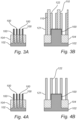
- Figures 1a and 1b show an example in which a hard mask layer 112 has been used to define the mandrels 110.
- the hard mask layer 112 may for example be formed of amorphous silicon, a-Si.
- each fin structure 100 is shown, of which the upper 50 nm may protrude from the isolation 104 on the substrate.
- the protruding part may also be referred to as the active region of the fins 100, in which the resulting transistor device may be formed.
- Each fin may in some examples have a width of 5-10 nm and be arranged next to each other, in a parallel fashion, at a pitch of for example 21-30 nm.
- the current example discloses three mandrels 110 arranged in a way that allows for mask layer to be formed, defining four gate tracks - two across the fin structures 100, and one on each side of the fin structures 100 (as seen in the length direction of the fins 100).
- This configuration which merely is to be regarded as an illustrative example of what may be enabled by the inventive concept, allows for a target gate line CD of 16 nm, given a spacer width of 6 nm, a gap/trench width of 14 nm and a total gate pitch of 42 nm.
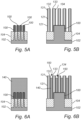
- Figure 2a shows a cross section of the structure of figures 1a and 1b , taken across the fin structures 100 at a position between two neighbouring mandrels 10 after a first spacer material 120 has been provided.
- the first spacer material 120 is provided on the mandrel 110.
- the spacer material 120 may be deposited as a conformal layer covering the entire mandrels 110.
- the first spacer material may be amorphous silicon deposited by means of ALD. It will be appreciated that the first spacer material can be provided directly on the mandrel material, or indirectly with an intermediate layer in between.
- the deposition method in which the first spacer material 120 is provided, may result in a conformal deposition of the material not only on the mandrels 110 but also on the fin structures 100. Therefore, the step of providing the first spacer material 120 may be followed by an etch-back process to remove the first spacer material from the fin structures 100.
- the result is shown in figures 3a and 3b , after the first spacer material 120 has been etched by for example an anisotropic etch to define a first set of spacers, including a first spacer 121 on a first side surface and a second spacer 122 on a second side surface of each one of the three mandrels 110 shown in the present example.
- the separation between the mandrels 110 in the current example may together with the thickness of the first spacer material 120, forming the first set of spacers, be selected such that a gap is defined between the spacers of adjacent mandrels 110.
- the width of the gap is selected to correspond to the width of the mandrels 110, such that the first set of spacers are arranged in an equidistant configuration.
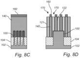
- Figures 4a and 4b show the first set of spacers 121, 122 after the mandrels 110 have been removed.
- the mandrels 110 may for example be removed by plasma stripping.
- the thickness and separation of the mandrels 110 may be selected such that the first set of spacers 121, 122 are provided with a constant separation.
- a second spacer material forming a second set of spacers 131, 132, 133, 134, has been provided on the first set of spacers 121, 122.
- the second spacer material may be provided directly on the first set of spacers 121, 122 or indirectly, with an intermediate layer in between.
- the second spacer material is formed as a conformal layer covering all surfaces of the first set of spacers 121, 122 the forming of the layer may be followed by an etch-back process so as to define the second set of spacers.
- the etch-back process may for example involve an anisotropic etch process similar to the one discussed above for the definition of the first set of spacers 121, 122.
- the result in shown in figures 5a and 5b in which the side surfaces of the first and second spacers 121, 122 has been provided with a respective spacer forming the second set of spacers 131, 132, 133, 134.
- the second set of spacers 131, 132, 133, 134 may for example be formed of a dielectric material, such as silicon nitride, or a low-k spacer of for example SiCO.
- the gaps between the second set of spacers 131, 132, 133, 134 may be filled with a first filler material 140.
- the first filler material 140 which for example may comprise a spin-on carbon material similar to the one discussed in connection with the mandrels, may be etched-back to form recesses 150 between the second set of spacers 131, 132, 133, 134. As shown in figures 6a and 6b , the recesses 150 may be provided at the very top portion of the second set of spacers 131, 132, 133, 134.
- the recesses 150 that extend in between may be considered as trenches extending along the spacers. As will be shown later on, the depth of the recesses 150 may determine the thickness of the final mask structure.
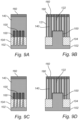
- a second filler material 160 such as for example silicon dioxide, has been provided in the recesses 150.
- the second filler material may be deposited on top of the structure shown in figures 7a and 7b and polished by means of for example CMP to expose the top surfaces of the first and second set of fins.
- the second filler material 160 that is provided in the recesses 150 may form dummy mask lines, which may be used later on for defining the mask lines of the final mask layer.
- Figures 8a-d , 9a-d and 10a-d illustrate steps for forming the final mask layer above the semiconductor fin structures 100.
- Two alternative example flows will be given; the first flow in the “a” and “b” figures, and the alternative flow in the "c” and “d” figures.
- a top portion 170 of at least the first set of spacers 121, 122 is recessed to form trenches extending along the spacers.
- the material of the first set of spacers 121, 122 is selectively etched with respect to the material of the second set of spacers 131, 132, 133, 134, such that the top portions 170 of the second set of spacers 131, 132, 133, 134 are preserved.
- the first spacer material is amorphous silicon and the second spacer material is silicon nitride
- the amorphous silicon may be selectively etched with respect to the neighbouring silicon nitride.
- the second spacer material is etched such that the recessing includes the top portions 170 of both the first set of spacers 121, 122 and the second set of spacers 131, 132, 133, 134.
- this is done in a single etch process that is capable of etching both materials, such as for example amorphous silicon and silicon nitride.
- two different etch processes may be used.
- Figures 9a to 9d show the structure after a mask layer material 180 has been provided between the dummy mask lines.
- the mask layer material 180 may for be silicon nitride, and may be provided in a recess filling process preferably followed by a CMP that stops on the material of the dummy mask lines.
- Figures 9a and 9b show the mask layer material 180 covering the underlying first set of spacers 121, 122, whereas figures 9c and 9d show the alternative flow in which the mask layer material 180 also covers the underlying second set of spacers 131, 132, 133, 134.
- Figures 10a to 10d show the mask layer 190 after the dummy mask lines have been removed together with the first filler material 140.
- the mask layer 190 is formed of the mask layer material 180 and the second set of spacers 131, 132, 133, 134, wherein the mask layer material 180 covering the underlying first set of spacers 121, 122.
- the mask layer 190 is formed of the mask layer material 180 covering both the first set of spacers 121, 122 and the second set of spacers 131, 132, 133, 134.
- the mask layer 190 may be ready for a subsequent replacement gate process for contacting the fin structures exposed in the gaps. This may include the formation of a dummy structure of for example oxide or nitride in place of the metal gate during high-temperature steps. After completion of those steps, which for example may include source/drain implant activation anneals, the dummy structure may be etched away, a gate dielectric grown or deposited, and the final metal gate deposited in the gate tracks defined between the spacers of the second set of spacers
Landscapes
- Insulated Gate Type Field-Effect Transistor (AREA)
- Semiconductor Memories (AREA)
Description
- The present inventive concept relates to the field of semiconductor processing. More specifically, it relates to a method for forming a mask layer above a semiconductor fin structure, wherein the mask layer enables the formation of gate structures for transistor devices formed in the fin structure.
- A transistor device, such as a Field Effect Transistor (FET), typically has a source, a channel and a drain, where current flows from the source to the drain, and a gate structure that controls the flow of current through the channel. The transistor device can have a variety of different structures. For example, transistors can be of a planar type with the source, channel and drain formed in the substrate material itself, or of a type in which the channel extends outward from the substrate. The channel can be an upright slab of thin material, commonly referred to as a fin, with a crossing gate structure arranged on the fin so as to control the flow of current along the fin, in the direction of a main surface of the substrate.
- With the ever decreasing device dimensions in the semiconductor industry, forming the individual components and features becomes more difficult. In the field of photolithography, the technique called Self Aligned Double Patterning (SADP) has been employed to form patterns of line widths that due to the scaling go beyond the optical limitations of conventional photolithography. SADP employs a technique called pitch splitting, in which the pattern is divided into two or more parts that can be processed conventionally and combined into the final, sub-resolution pitch pattern.
- The SADP approach is known to be used for providing fin-transistor gate structures having a reduced critical dimension. However, there is still a need for an improved process that is capable of meeting the ever increasing demands put on gate pitch scaling, footprint reduction and process reliability.
- An example of a FET is disclosed in
US 2019/013396 A1 . The FET includes a substrate, a semiconductor fin, a first gate stack, and a first metal element-containing dielectric mask. The semiconductor fin protrudes from the substrate. The first gate stack is over the semiconductor fin. The first metal element-containing dielectric mask is over the first gate stack. - An objective of the present inventive concept is to provide a method for forming a mask layer above a semiconductor fin structure. Further and/or alternative objectives may be understood from the following.
- According to an aspect of the present inventive concept there is provided method for forming a mask layer above a semiconductor fin structure, the method comprising:
- forming a mandrel above the fin structure,
- providing a first spacer material on the mandrel, thereby forming a first set of spacers including a first spacer at a first side surface of the mandrel and a second spacer at a second side surface of the mandrel,
- removing the mandrel,
- providing a second spacer material on the first and the second spacers, thereby forming a second set of spacers arranged at the side surfaces of the first set of spacers,
- providing a first filler material between the second set of spacers,
- etching a top portion of the first filler material to form recesses between the second set of spacers,
- providing a second filler material in the recesses, the second filler material forming a set of dummy mask lines,
- recessing a top portion of at least the first set of spacers,
- providing a mask layer material between the dummy mask lines, and
- removing the dummy mask lines and the first filler material.
- In modern device fabrication, advanced gate patterning may include multiple patterning processes such as Self Aligned Double Patterning (SADP) or Self Aligned Quadruple Patterning (SAQP) for defining the gate critical dimension (CD). The present inventive concept makes use of a different approach, in which a similar gate CD may be provided without necessarily employing a multiple patterning process. Instead, the mandrel can be formed in a direct patterning process and the gate CD defined by the first set and second set of spacers that are positioned by means of the mandrel. The fact that the same gate CD may be provided without using a multiple patterning process makes further scaling feasible.
- Further, the present inventive concept allows for the mask layer to be provided after the first and second set of spacers have been formed. This is advantageous over multiple patterning techniques that tend to use the same hard mask both for the multiple patterning process and the final gate mask layer, since the hard mask in those cases risks to be damaged or over etched during in particular the recessing of the spacer. By instead forming the final mask layer after the processing of the first and second set of spacers, the mask layer may be designed without taking process requirements related to the forming of the spacers into account. Instead, the mask layer may be engineered with respect to requirements associated with subsequent processing of the gate structures, such as for example replacement dummy gate processing. In particular, the mask layer may be adapted to have an improved etch resistance and/or be an improved chemical-mechanical polishing (CMP) stopping layer.
- The fin structure may be a fin-shaped semiconductor structure extending along and protruding above a substrate. Even though the present aspect mentions "a semiconductor fin structure", it is appreciated that the inventive concept is applicable also to a plurality of semiconductor fin structures, such as a first fin structure and a second fin structure. The first fin structure may extend along a first fin track (i.e. a first geometrical straight line along the substrate). The second fin structure may extend along a second fin track (i.e. a second geometrical straight line along the substrate). The first fin structure and the second fin structure may extend in parallel to each other.
- One or several transistor devices can be formed in the fin structure. Such a transistor device may for example be a field-effect transistor, FET, also referred to as a finFET, having a source region and a drain region formed in the fin and a horizontal channel in between.
- By "mandrel" is hereby meant a core or feature that may be used as support for subsequent growth or deposition of the first spacer material. The mandrel may be formed in a single patterning step using a same mask, or in a multiple patterning process using several sub-masks. The patterning may be performed on a mandrel material layer that is formed above the fin structure. The mandrel material layer may be arranged directly on the fin structure or on an intermediate layer. In embodiments, the mandrel may be oriented across the fin structure, such as substantially orthogonal, thereby allowing the final gate structures to be formed across the fin structure.
- The first set of spacers may be formed by depositing the first spacer material over the mandrel, preferably as a conformal layer, and etching the deposited first spacer material such that the first spacer material remains at least on part of the side surfaces of the mandrel, thereby forming the first set of spacers. The etch may for example be anisotropic, leaving the first spacer material on the side surfaces of the mandrel.
- The second set of spacers may be formed in a similar way, i.e., by depositing the second spacer material over the first set of spacers (after removal of the mandrel). The second spacer material may be deposited as a conformal layer, and etch such that the second spacer material remains at least on part of the side surfaces of the first set of spacers.
- The first spacer material and the second spacer material may be etch-selective relative each other, such that for example the first spacer material can be etched away while the second spacer material is preserved.
- By the terminology "mask layer" may be understood a layer that is capable of counteracting etching in regions covered by the layer. Regions exposed by the etch mask may accordingly be etched while regions covered by the etch mask need not be affected appreciably. Alternatively, or additionally, a mask layer may be understood as a pattern or structure that allows features to be defined in a subsequent processing step in which a material is added by means of for example growth or deposition. Regions exposed by the mask layer may be provided with the added material, while the covered regions may be protected from the added material. In the context of the present application, the mask layer formed in the method according to the inventive concept may define a plurality of line-shaped gaps in which for example dummy gates or metal gates may be provided.
- A material may be etch-selective relative to another material. By etching or removal of a feature "A" selectively to a feature "B" is hereby meat that a feature A arranged adjacent to a feature B may be removed while preserving the feature B. This may be achieved by covering the feature B to be preserved by an etch mask. This may also be achieved by exposing the features A and B to an etch process wherein the feature A is etched at a greater rate than the feature B. Hence, portions of the feature A exposed to the etching process may be removed while portions of the feature B exposed to the etch process may be preserved. The preservation of the feature B following the etch process may be complete (in the sense that the feature B is not affected appreciably during the etch process) or at least partial (in the sense that the feature B remains at least to the extent that it may serve its intended function during subsequent process steps). A ratio of an etch rate of the material of feature B may advantageously be 2:1 or higher, but more preferably 10:1 or higher, or even more preferably 40:1 or higher.
- By the term "above" is hereby meant a relative position as viewed in a normal direction from the main surface of the substrate. The terminology "above" does hence not refer to an absolute orientation of the layers or features, but to a relative ordering thereof. Accordingly, "side" or "side surface" may refer to a surface or surface portion facing in a direction along the main surface of the substrate. Put differently, the term "side surface" may have a normal direction that is orthogonal to the normal direction from the main surface of the substrate.
- According to an embodiment, the mandrel may be formed by a carbon based material, such as for example a spin-on carbon (SoC), photoresist, bottom antireflective coating (BARC) or advanced patterning film (APF). These types of materials may be advantageous over for example siliconbased materials, since they generally are better suited for high-aspect-ratio patterning and tend to be possible to etch while maintaining a relative straight profile of the resulting mandrel. SoC may be particularly advantageous in that it allows for a planarization, in which the fin topography may be polished and flattened by means of for example CMP. APF, on the other hand, may withstand higher temperatures compared to for example SoC, BARC and photoresist.
- According to an embodiment, the first spacer material may be provided by means of an atomic layer deposition (ALD) process. The first spacer material may for example be amorphous silicon (a-Si). ALD may be advantageous over for example chemical vapour deposition (CVD), since it allows for a relatively conformal deposition of material and a relatively easy layer deposition control. CVD has shown to generate more voids and irregularities in the deposited material.
- According to an embodiment, the step of providing the first spacer material may be followed by an etch-back process for removing the first spacer material that has been deposited on the fin structure. This may be performed in an etch process that removes the first spacer material provided on top of and between the first set of spacers, while leaving at least some of the first spacer material on the side surfaces of the first spacer and the second spacer.
- According to an embodiment, the second spacer material may comprise a material that is etch selective relative the first spacer material. The second spacer material may in an example be a dielectric material such as for example silicon nitride, or a low-k dielectric such as SiCO or SiOCN. The second spacer material may be provided after the mandrel has been stripped or removed, such that the second set of spacers are formed at the side surfaces of the first set of spacers. In a subsequent step, the second spacer material may be etched-back to remove the second spacer material from the fin structure, leaving the second spacer material as spacers on the first set of spacers.
- At this stage of the process, a set of mask lines or gaps may be provided, wherein the thickness of the mask lines may be determined by the thickness and separation of the first set of spacers and by the thickness of the second spacer material deposited on the sides of the first set of spacers. The width of the gaps may determine the width or critical dimension of the final gate line provided by means of the mask layer that may result from the present inventive concept.
- According to an embodiment, the first filler material, which may be provided between the second set of spacers, may be a carbon based material similar to the one discussed above in connection with the material of the mandrel.
- The first filler material may be etched back so as to allow recesses to be formed between the second set of spacers. These recesses may then be filled with the second filler material, which for example may be silicon dioxide, thereby forming the set of dummy mask lines. Preferably, a top portion of the first filler material is removed, the size of the top portion determining the height of the dummy mask lines and thus the thickness of the final mask layer.
- According to an embodiment, not only the first set of spacers but also the top of the second set of spacers may be recessed prior to providing the mask layer material between the dummy mask lines. As a result, the mask layer may protect not only the underlying first set of spacers but also the second set of spacers arranged on the side surfaces of the first set of spacers. The mask layer may for example comprise SiO2, Si3N4, SiCO or SiOCN, a metal or metal oxide such as titanium nitride, titanium dioxide or hafnium dioxide.
- The present inventive concept may be employed in replacement dummy gate processing, in which a dummy structure of for example oxide or nitride may serve in place of the metal gate during high-temperature steps. After completion of those steps, which for example may include source/drain implant activation anneals, the dummy structure may be etched away, a gate dielectric grown or deposited, and the final metal gate deposited in the gate tracks defined between the spacers of the second set of spacers.
- The above, as well as additional objects, features and advantages of the present inventive concept, will be better understood through the following illustrative and non-limiting detailed description, with reference to the appended drawings. In the drawings like reference numerals will be used for like elements unless stated otherwise.
-
Figures 1a , b; 2a, 2b; ...7a, b and 8a-d, 9a-d and 10a-d schematically illustrate a method for forming a mask layer above a semiconductor fin structure according to one or more embodiments of the present inventive concept. - As illustrated in the figures, the sizes of the layers, features and other structures may be exaggerated or not depicted proportionally for illustrative purposes. Thus, the figures are provided to illustrate the general elements of the embodiments.
- In the drawings, like reference numerals will be used for like elements unless stated otherwise.
- A method for forming a mask layer will now be described with reference to the appended drawings, wherein the "a" figures generally show cross sections taken across the fin structure and the "b" figures generally show cross sections taken along the fin structure.
- A cross section taken across a plurality of
fin structures 100 is disclosed infigure 1a. Figure 1b is a cross section taken along one of thefin structures 100. In the following, features of the inventive concept will be discussed with reference to bothfigure 1a and figure 1b . - Each of the
fin structures 100 may be arranged on asubstrate 102, thesubstrate 102 having a main surface extending along a plane coinciding with a length direction of thefin structures 100. Thefin structures 100 may for example be formed by patterning of thesubstrate 102 and/or by means of epitaxial growth. Thesubstrate 102 and thefin structures 100 may for example be formed of silicon. As indicated infigure 1a , an isolatinglayer 104, such as a shallow trench isolation, may be provided on thesubstrate 102 such that only an upper part of thefin structures 100 protrudes above a top surface of the isolatinglayer 104. - A
mandrel 110 is provided above thefin structures 100. The mandrel may be formed as a core or elongated feature extending across thefin structures 100, in a transversal direction coinciding with the orientation of the gate tracks of the final device (not shown in the present figures). Themandrel 110 may be formed by a spin-on deposited carbon based material, such as for example spin-on carbon (SoC) or Advanced Patterning Film (APF) from Applied Materials. One orseveral mandrels 110 may be provided; the number depending on the desired mask pattern to be formed. In the example shown in presentfigure 1b , three mandrels are indicated. Themandrels 110 may be formed in a direct patterning process, in which a single lithographic step may be used, or in a multiple patterning process such as the previously described SADP and SAQP examples.Figures 1a and 1b show an example in which ahard mask layer 112 has been used to define themandrels 110. Thehard mask layer 112 may for example be formed of amorphous silicon, a-Si. - In the current, illustrative example, four
fin structures 100 are shown, of which the upper 50 nm may protrude from theisolation 104 on the substrate. The protruding part may also be referred to as the active region of thefins 100, in which the resulting transistor device may be formed. Each fin may in some examples have a width of 5-10 nm and be arranged next to each other, in a parallel fashion, at a pitch of for example 21-30 nm. - Turning to the
mandrels 110, the current example discloses threemandrels 110 arranged in a way that allows for mask layer to be formed, defining four gate tracks - two across thefin structures 100, and one on each side of the fin structures 100 (as seen in the length direction of the fins 100). This configuration, which merely is to be regarded as an illustrative example of what may be enabled by the inventive concept, allows for a target gate line CD of 16 nm, given a spacer width of 6 nm, a gap/trench width of 14 nm and a total gate pitch of 42 nm. -
Figure 2a shows a cross section of the structure offigures 1a and 1b , taken across thefin structures 100 at a position between two neighbouring mandrels 10 after afirst spacer material 120 has been provided. Thefirst spacer material 120 is provided on themandrel 110. Thespacer material 120 may be deposited as a conformal layer covering theentire mandrels 110. In one example, the first spacer material may be amorphous silicon deposited by means of ALD. It will be appreciated that the first spacer material can be provided directly on the mandrel material, or indirectly with an intermediate layer in between. - The deposition method, in which the
first spacer material 120 is provided, may result in a conformal deposition of the material not only on themandrels 110 but also on thefin structures 100. Therefore, the step of providing thefirst spacer material 120 may be followed by an etch-back process to remove the first spacer material from thefin structures 100. The result is shown infigures 3a and 3b , after thefirst spacer material 120 has been etched by for example an anisotropic etch to define a first set of spacers, including afirst spacer 121 on a first side surface and asecond spacer 122 on a second side surface of each one of the threemandrels 110 shown in the present example. - The separation between the
mandrels 110 in the current example may together with the thickness of thefirst spacer material 120, forming the first set of spacers, be selected such that a gap is defined between the spacers ofadjacent mandrels 110. Preferably, the width of the gap is selected to correspond to the width of themandrels 110, such that the first set of spacers are arranged in an equidistant configuration. -
Figures 4a and 4b show the first set ofspacers mandrels 110 have been removed. Themandrels 110 may for example be removed by plasma stripping. As mentioned above, the thickness and separation of themandrels 110 may be selected such that the first set ofspacers - In
figures 5a and 5b , a second spacer material , forming a second set ofspacers spacers spacers spacers spacers - The result in shown in
figures 5a and 5b , in which the side surfaces of the first andsecond spacers spacers spacers - In a subsequent step, the gaps between the second set of
spacers first filler material 140. Thefirst filler material 140, which for example may comprise a spin-on carbon material similar to the one discussed in connection with the mandrels, may be etched-back to formrecesses 150 between the second set ofspacers figures 6a and 6b , therecesses 150 may be provided at the very top portion of the second set ofspacers spacers recesses 150 that extend in between may be considered as trenches extending along the spacers. As will be shown later on, the depth of therecesses 150 may determine the thickness of the final mask structure. - In
figures 7a and 7b , asecond filler material 160, such as for example silicon dioxide, has been provided in therecesses 150. The second filler material may be deposited on top of the structure shown infigures 7a and 7b and polished by means of for example CMP to expose the top surfaces of the first and second set of fins. Thesecond filler material 160 that is provided in therecesses 150 may form dummy mask lines, which may be used later on for defining the mask lines of the final mask layer. -
Figures 8a-d ,9a-d and10a-d illustrate steps for forming the final mask layer above thesemiconductor fin structures 100. Two alternative example flows will be given; the first flow in the "a" and "b" figures, and the alternative flow in the "c" and "d" figures. - After the
second filler material 160 has been provided to form the dummy mask lines, atop portion 170 of at least the first set ofspacers figures 8a and 8b , the material of the first set ofspacers spacers top portions 170 of the second set ofspacers - In
figures 8c and 8d , also the second spacer material is etched such that the recessing includes thetop portions 170 of both the first set ofspacers spacers -
Figures 9a to 9d show the structure after amask layer material 180 has been provided between the dummy mask lines. Themask layer material 180 may for be silicon nitride, and may be provided in a recess filling process preferably followed by a CMP that stops on the material of the dummy mask lines.Figures 9a and 9b show themask layer material 180 covering the underlying first set ofspacers figures 9c and 9d show the alternative flow in which themask layer material 180 also covers the underlying second set ofspacers -
Figures 10a to 10d show themask layer 190 after the dummy mask lines have been removed together with thefirst filler material 140. Infigures 10a and 10b , themask layer 190 is formed of themask layer material 180 and the second set ofspacers mask layer material 180 covering the underlying first set ofspacers figures 10c and 10d , themask layer 190 is formed of themask layer material 180 covering both the first set ofspacers spacers - By removing the first filler material in the gaps defined between the second set of spacers, the
mask layer 190 may be ready for a subsequent replacement gate process for contacting the fin structures exposed in the gaps. This may include the formation of a dummy structure of for example oxide or nitride in place of the metal gate during high-temperature steps. After completion of those steps, which for example may include source/drain implant activation anneals, the dummy structure may be etched away, a gate dielectric grown or deposited, and the final metal gate deposited in the gate tracks defined between the spacers of the second set of spacers - In the above the inventive concept has mainly been described with reference to a limited number of examples. However, as is readily appreciated by a person skilled in the art, other examples than the ones disclosed above are equally possible as long as they fall within the scope of the inventive concept, as defined by the appended claims.
Claims (11)
- A method for forming a mask layer (190) above a semiconductor fin structure (100), comprising:forming a mandrel (110) above the fin structure;providing a first spacer material (120) on the mandrel, thereby forming a first set of spacers including a first spacer (121) at a first side surface of the mandrel and a second spacer (122) at a second side surface of the mandrel;removing the mandrel;providing a second spacer material (130) on the first and the second spacers, thereby forming a second set of spacers (131, 132, 133, 134) arranged at the side surfaces of the first set of spacers;providing a first filler material (140) between the second set of spacers;etching a top portion of the first filler material to form recesses (150) between the second set of spacers;providing a second filler material (160) in the recesses, the second filler material forming a set of dummy mask lines;recessing a top portion (170) of at least the first set of spacers;providing a mask layer material (180) between the dummy mask lines; andremoving the dummy mask lines and the first filler material.
- A method according to claim 1, wherein the mandrel is formed by a spin-on carbon material.
- A method according to any one of the preceding claims, wherein the first spacer material is provided by means of an atomic layer deposition, ALD, process.
- A method according to claim 3, wherein the first spacer material comprises amorphous silicon.
- A method according to any one of the preceding claims, wherein the step of providing the first spacer material is followed by an etch-back process to remove the first spacer material from the fin structure.
- A method according to any one of the preceding claims, wherein the second spacer material comprises a dielectric material, such as silicon nitride.
- A method according to claim 6, wherein the step of providing the second spacer material is followed by an etch-back process to remove the second spacer material from the fin structure.
- A method according to any one of the preceding claims, wherein the first filler material comprises a spin-on carbon material.
- A method according to any one of the preceding claims, further comprising recessing a top portion of the second set of spacers prior to providing the mask layer material between the dummy mask lines.
- A method according to any one of the preceding claims, wherein the second filler material comprises silicon dioxide.
- A method according to any one of the preceding claims, wherein the mask layer comprises silicon dioxide or hafnium dioxide.
Priority Applications (4)
| Application Number | Priority Date | Filing Date | Title |
|---|---|---|---|
| EP19168018.0A EP3723112B1 (en) | 2019-04-09 | 2019-04-09 | Method for forming a gate mask layer |
| TW109110325A TWI892983B (en) | 2019-04-09 | 2020-03-26 | Method for forming a mask layer above a semiconductor fin structure |
| US16/843,706 US11430697B2 (en) | 2019-04-09 | 2020-04-08 | Method of forming a mask layer |
| CN202010269219.7A CN111799157B (en) | 2019-04-09 | 2020-04-08 | Method for forming a mask layer on a semiconductor fin structure |
Applications Claiming Priority (1)
| Application Number | Priority Date | Filing Date | Title |
|---|---|---|---|
| EP19168018.0A EP3723112B1 (en) | 2019-04-09 | 2019-04-09 | Method for forming a gate mask layer |
Publications (2)
| Publication Number | Publication Date |
|---|---|
| EP3723112A1 EP3723112A1 (en) | 2020-10-14 |
| EP3723112B1 true EP3723112B1 (en) | 2023-12-20 |
Family
ID=66286066
Family Applications (1)
| Application Number | Title | Priority Date | Filing Date |
|---|---|---|---|
| EP19168018.0A Active EP3723112B1 (en) | 2019-04-09 | 2019-04-09 | Method for forming a gate mask layer |
Country Status (4)
| Country | Link |
|---|---|
| US (1) | US11430697B2 (en) |
| EP (1) | EP3723112B1 (en) |
| CN (1) | CN111799157B (en) |
| TW (1) | TWI892983B (en) |
Families Citing this family (2)
| Publication number | Priority date | Publication date | Assignee | Title |
|---|---|---|---|---|
| CN112017947A (en) * | 2020-07-17 | 2020-12-01 | 中国科学院微电子研究所 | A method of manufacturing a semiconductor structure |
| US11424124B2 (en) * | 2020-11-05 | 2022-08-23 | Nanya Technology Corporation | Method of forming a patterned hard mask and method of forming conductive lines |
Family Cites Families (25)
| Publication number | Priority date | Publication date | Assignee | Title |
|---|---|---|---|---|
| US20050070103A1 (en) * | 2003-09-29 | 2005-03-31 | Applied Materials, Inc. | Method and apparatus for endpoint detection during an etch process |
| US7759197B2 (en) * | 2005-09-01 | 2010-07-20 | Micron Technology, Inc. | Method of forming isolated features using pitch multiplication |
| US7790531B2 (en) * | 2007-12-18 | 2010-09-07 | Micron Technology, Inc. | Methods for isolating portions of a loop of pitch-multiplied material and related structures |
| US8492282B2 (en) * | 2008-11-24 | 2013-07-23 | Micron Technology, Inc. | Methods of forming a masking pattern for integrated circuits |
| US8110466B2 (en) * | 2009-10-27 | 2012-02-07 | Taiwan Semiconductor Manufacturing Company, Ltd. | Cross OD FinFET patterning |
| US8222100B2 (en) * | 2010-01-15 | 2012-07-17 | International Business Machines Corporation | CMOS circuit with low-k spacer and stress liner |
| US8962484B2 (en) * | 2011-12-16 | 2015-02-24 | Taiwan Semiconductor Manufacturing Company, Ltd. | Method of forming pattern for semiconductor device |
| US9177820B2 (en) * | 2012-10-24 | 2015-11-03 | Globalfoundries U.S. 2 Llc | Sub-lithographic semiconductor structures with non-constant pitch |
| US9304396B2 (en) * | 2013-02-25 | 2016-04-05 | Lam Research Corporation | PECVD films for EUV lithography |
| US8932955B1 (en) | 2013-09-04 | 2015-01-13 | Sandisk Technologies Inc. | Triple patterning NAND flash memory with SOC |
| US9640625B2 (en) * | 2014-04-25 | 2017-05-02 | Globalfoundries Inc. | Self-aligned gate contact formation |
| US9123656B1 (en) | 2014-05-13 | 2015-09-01 | Taiwan Semiconductor Manufacturing Co., Ltd. | Organosilicate polymer mandrel for self-aligned double patterning process |
| US9287135B1 (en) * | 2015-05-26 | 2016-03-15 | International Business Machines Corporation | Sidewall image transfer process for fin patterning |
| US9548243B1 (en) * | 2015-06-30 | 2017-01-17 | International Business Machines Corporation | Self aligned via and pillar cut for at least a self aligned double pitch |
| US9530772B1 (en) * | 2015-08-06 | 2016-12-27 | International Business Machines Corporation | Methods of manufacturing devices including gates with multiple lengths |
| US9934985B2 (en) * | 2015-11-30 | 2018-04-03 | Taiwan Semiconductor Manufacturing Company, Ltd. | Critical dimension control for double patterning process |
| US9679809B1 (en) | 2016-03-22 | 2017-06-13 | Globalfoundries Inc. | Method of forming self aligned continuity blocks for mandrel and non-mandrel interconnect lines |
| US9741821B1 (en) | 2016-03-24 | 2017-08-22 | Taiwan Semiconductor Manufacturing Company, Ltd. | Two-step dummy gate formation |
| US9881794B1 (en) * | 2016-11-29 | 2018-01-30 | Taiwan Semiconductor Manufacturing Company, Ltd. | Semiconductor methods and devices |
| US9934970B1 (en) * | 2017-01-11 | 2018-04-03 | International Business Machines Corporation | Self aligned pattern formation post spacer etchback in tight pitch configurations |
| US10056473B1 (en) * | 2017-04-07 | 2018-08-21 | Taiwan Semiconductor Manufacturing Co., Ltd. | Semiconductor device and manufacturing method thereof |
| US10600687B2 (en) * | 2017-04-19 | 2020-03-24 | Tokyo Electron Limited | Process integration techniques using a carbon layer to form self-aligned structures |
| US10276378B1 (en) * | 2017-10-30 | 2019-04-30 | Taiwan Semiconductor Manufacturing Co., Ltd. | Method of forming funnel-like opening for semiconductor device structure |
| US10593870B2 (en) * | 2017-12-14 | 2020-03-17 | International Business Machines Corporation | Sidewall image transfer on magnetic tunnel junction stack for magnetoresistive random-access memory patterning |
| KR102781732B1 (en) * | 2019-04-12 | 2025-03-13 | 도쿄엘렉트론가부시키가이샤 | Substrate processing method using multi-line patterning |
-
2019
- 2019-04-09 EP EP19168018.0A patent/EP3723112B1/en active Active
-
2020
- 2020-03-26 TW TW109110325A patent/TWI892983B/en active
- 2020-04-08 CN CN202010269219.7A patent/CN111799157B/en active Active
- 2020-04-08 US US16/843,706 patent/US11430697B2/en active Active
Also Published As
| Publication number | Publication date |
|---|---|
| CN111799157A (en) | 2020-10-20 |
| US11430697B2 (en) | 2022-08-30 |
| EP3723112A1 (en) | 2020-10-14 |
| CN111799157B (en) | 2025-10-21 |
| TWI892983B (en) | 2025-08-11 |
| TW202044408A (en) | 2020-12-01 |
| US20200328122A1 (en) | 2020-10-15 |
Similar Documents
| Publication | Publication Date | Title |
|---|---|---|
| US10504798B2 (en) | Gate cut in replacement metal gate process | |
| US9490129B2 (en) | Integrated circuits having improved gate structures and methods for fabricating same | |
| US10283415B2 (en) | Semiconductor structure with a bump having a width larger than a width of fin shaped structures and manufacturing method thereof | |
| KR100546378B1 (en) | Method for manufacturing a transistor having a recess channel | |
| US9601335B2 (en) | Trench formation for dielectric filled cut region | |
| CN110739210A (en) | Semiconductor structure and forming method thereof | |
| US10177037B2 (en) | Methods of forming a CT pillar between gate structures in a semiconductor | |
| US20150076624A1 (en) | Integrated circuits having smooth metal gates and methods for fabricating same | |
| US10854452B2 (en) | Method of manufacturing semiconductor devices | |
| US20180047575A1 (en) | Self-aligned single dummy fin cut with tight pitch | |
| US20210225657A1 (en) | Hard Mask Removal Method | |
| US11037788B2 (en) | Integration of device regions | |
| US11430697B2 (en) | Method of forming a mask layer | |
| KR102882048B1 (en) | Self-aligned top via formation at line ends | |
| US10483395B2 (en) | Method for fabricating semiconductor device | |
| US9847423B1 (en) | Semiconductor device and method for fabricating the same | |
| CN111696864B (en) | Semiconductor devices and methods of forming the same | |
| CN112687622A (en) | Single diffusion region cutting structure of fin field effect transistor and forming method thereof | |
| US12261045B2 (en) | Patterning method | |
| EP3309842A1 (en) | A semiconductor apparatus and manufacturing method | |
| CN118511282A (en) | Power device structure and manufacturing method | |
| US10707198B2 (en) | Patterning a target layer | |
| CN121038355A (en) | Semiconductor structure and its formation method |
Legal Events
| Date | Code | Title | Description |
|---|---|---|---|
| PUAI | Public reference made under article 153(3) epc to a published international application that has entered the european phase |
Free format text: ORIGINAL CODE: 0009012 |
|
| STAA | Information on the status of an ep patent application or granted ep patent |
Free format text: STATUS: THE APPLICATION HAS BEEN PUBLISHED |
|
| AK | Designated contracting states |
Kind code of ref document: A1 Designated state(s): AL AT BE BG CH CY CZ DE DK EE ES FI FR GB GR HR HU IE IS IT LI LT LU LV MC MK MT NL NO PL PT RO RS SE SI SK SM TR |
|
| AX | Request for extension of the european patent |
Extension state: BA ME |
|
| STAA | Information on the status of an ep patent application or granted ep patent |
Free format text: STATUS: REQUEST FOR EXAMINATION WAS MADE |
|
| 17P | Request for examination filed |
Effective date: 20210323 |
|
| RBV | Designated contracting states (corrected) |
Designated state(s): AL AT BE BG CH CY CZ DE DK EE ES FI FR GB GR HR HU IE IS IT LI LT LU LV MC MK MT NL NO PL PT RO RS SE SI SK SM TR |
|
| GRAP | Despatch of communication of intention to grant a patent |
Free format text: ORIGINAL CODE: EPIDOSNIGR1 |
|
| STAA | Information on the status of an ep patent application or granted ep patent |
Free format text: STATUS: GRANT OF PATENT IS INTENDED |
|
| RAP3 | Party data changed (applicant data changed or rights of an application transferred) |
Owner name: IMEC VZW |
|
| INTG | Intention to grant announced |
Effective date: 20230718 |
|
| P01 | Opt-out of the competence of the unified patent court (upc) registered |
Effective date: 20230804 |
|
| GRAS | Grant fee paid |
Free format text: ORIGINAL CODE: EPIDOSNIGR3 |
|
| GRAA | (expected) grant |
Free format text: ORIGINAL CODE: 0009210 |
|
| STAA | Information on the status of an ep patent application or granted ep patent |
Free format text: STATUS: THE PATENT HAS BEEN GRANTED |
|
| AK | Designated contracting states |
Kind code of ref document: B1 Designated state(s): AL AT BE BG CH CY CZ DE DK EE ES FI FR GB GR HR HU IE IS IT LI LT LU LV MC MK MT NL NO PL PT RO RS SE SI SK SM TR |
|
| REG | Reference to a national code |
Ref country code: GB Ref legal event code: FG4D |
|
| REG | Reference to a national code |
Ref country code: CH Ref legal event code: EP |
|
| REG | Reference to a national code |
Ref country code: DE Ref legal event code: R096 Ref document number: 602019043471 Country of ref document: DE |
|
| REG | Reference to a national code |
Ref country code: IE Ref legal event code: FG4D |
|
| PG25 | Lapsed in a contracting state [announced via postgrant information from national office to epo] |
Ref country code: GR Free format text: LAPSE BECAUSE OF FAILURE TO SUBMIT A TRANSLATION OF THE DESCRIPTION OR TO PAY THE FEE WITHIN THE PRESCRIBED TIME-LIMIT Effective date: 20240321 |
|
| REG | Reference to a national code |
Ref country code: LT Ref legal event code: MG9D |
|
| PG25 | Lapsed in a contracting state [announced via postgrant information from national office to epo] |
Ref country code: LT Free format text: LAPSE BECAUSE OF FAILURE TO SUBMIT A TRANSLATION OF THE DESCRIPTION OR TO PAY THE FEE WITHIN THE PRESCRIBED TIME-LIMIT Effective date: 20231220 |
|
| REG | Reference to a national code |
Ref country code: NL Ref legal event code: MP Effective date: 20231220 |
|
| PG25 | Lapsed in a contracting state [announced via postgrant information from national office to epo] |
Ref country code: ES Free format text: LAPSE BECAUSE OF FAILURE TO SUBMIT A TRANSLATION OF THE DESCRIPTION OR TO PAY THE FEE WITHIN THE PRESCRIBED TIME-LIMIT Effective date: 20231220 |
|
| PG25 | Lapsed in a contracting state [announced via postgrant information from national office to epo] |
Ref country code: LT Free format text: LAPSE BECAUSE OF FAILURE TO SUBMIT A TRANSLATION OF THE DESCRIPTION OR TO PAY THE FEE WITHIN THE PRESCRIBED TIME-LIMIT Effective date: 20231220 Ref country code: GR Free format text: LAPSE BECAUSE OF FAILURE TO SUBMIT A TRANSLATION OF THE DESCRIPTION OR TO PAY THE FEE WITHIN THE PRESCRIBED TIME-LIMIT Effective date: 20240321 Ref country code: FI Free format text: LAPSE BECAUSE OF FAILURE TO SUBMIT A TRANSLATION OF THE DESCRIPTION OR TO PAY THE FEE WITHIN THE PRESCRIBED TIME-LIMIT Effective date: 20231220 Ref country code: ES Free format text: LAPSE BECAUSE OF FAILURE TO SUBMIT A TRANSLATION OF THE DESCRIPTION OR TO PAY THE FEE WITHIN THE PRESCRIBED TIME-LIMIT Effective date: 20231220 Ref country code: BG Free format text: LAPSE BECAUSE OF FAILURE TO SUBMIT A TRANSLATION OF THE DESCRIPTION OR TO PAY THE FEE WITHIN THE PRESCRIBED TIME-LIMIT Effective date: 20240320 |
|
| REG | Reference to a national code |
Ref country code: AT Ref legal event code: MK05 Ref document number: 1643193 Country of ref document: AT Kind code of ref document: T Effective date: 20231220 |
|
| PG25 | Lapsed in a contracting state [announced via postgrant information from national office to epo] |
Ref country code: NL Free format text: LAPSE BECAUSE OF FAILURE TO SUBMIT A TRANSLATION OF THE DESCRIPTION OR TO PAY THE FEE WITHIN THE PRESCRIBED TIME-LIMIT Effective date: 20231220 |
|
| PG25 | Lapsed in a contracting state [announced via postgrant information from national office to epo] |
Ref country code: SE Free format text: LAPSE BECAUSE OF FAILURE TO SUBMIT A TRANSLATION OF THE DESCRIPTION OR TO PAY THE FEE WITHIN THE PRESCRIBED TIME-LIMIT Effective date: 20231220 Ref country code: RS Free format text: LAPSE BECAUSE OF FAILURE TO SUBMIT A TRANSLATION OF THE DESCRIPTION OR TO PAY THE FEE WITHIN THE PRESCRIBED TIME-LIMIT Effective date: 20231220 Ref country code: NO Free format text: LAPSE BECAUSE OF FAILURE TO SUBMIT A TRANSLATION OF THE DESCRIPTION OR TO PAY THE FEE WITHIN THE PRESCRIBED TIME-LIMIT Effective date: 20240320 Ref country code: NL Free format text: LAPSE BECAUSE OF FAILURE TO SUBMIT A TRANSLATION OF THE DESCRIPTION OR TO PAY THE FEE WITHIN THE PRESCRIBED TIME-LIMIT Effective date: 20231220 Ref country code: LV Free format text: LAPSE BECAUSE OF FAILURE TO SUBMIT A TRANSLATION OF THE DESCRIPTION OR TO PAY THE FEE WITHIN THE PRESCRIBED TIME-LIMIT Effective date: 20231220 Ref country code: HR Free format text: LAPSE BECAUSE OF FAILURE TO SUBMIT A TRANSLATION OF THE DESCRIPTION OR TO PAY THE FEE WITHIN THE PRESCRIBED TIME-LIMIT Effective date: 20231220 |
|
| PG25 | Lapsed in a contracting state [announced via postgrant information from national office to epo] |
Ref country code: IS Free format text: LAPSE BECAUSE OF FAILURE TO SUBMIT A TRANSLATION OF THE DESCRIPTION OR TO PAY THE FEE WITHIN THE PRESCRIBED TIME-LIMIT Effective date: 20240420 |
|
| PG25 | Lapsed in a contracting state [announced via postgrant information from national office to epo] |
Ref country code: CZ Free format text: LAPSE BECAUSE OF FAILURE TO SUBMIT A TRANSLATION OF THE DESCRIPTION OR TO PAY THE FEE WITHIN THE PRESCRIBED TIME-LIMIT Effective date: 20231220 Ref country code: AT Free format text: LAPSE BECAUSE OF FAILURE TO SUBMIT A TRANSLATION OF THE DESCRIPTION OR TO PAY THE FEE WITHIN THE PRESCRIBED TIME-LIMIT Effective date: 20231220 |
|
| PG25 | Lapsed in a contracting state [announced via postgrant information from national office to epo] |
Ref country code: SK Free format text: LAPSE BECAUSE OF FAILURE TO SUBMIT A TRANSLATION OF THE DESCRIPTION OR TO PAY THE FEE WITHIN THE PRESCRIBED TIME-LIMIT Effective date: 20231220 |
|
| PG25 | Lapsed in a contracting state [announced via postgrant information from national office to epo] |
Ref country code: SM Free format text: LAPSE BECAUSE OF FAILURE TO SUBMIT A TRANSLATION OF THE DESCRIPTION OR TO PAY THE FEE WITHIN THE PRESCRIBED TIME-LIMIT Effective date: 20231220 Ref country code: SK Free format text: LAPSE BECAUSE OF FAILURE TO SUBMIT A TRANSLATION OF THE DESCRIPTION OR TO PAY THE FEE WITHIN THE PRESCRIBED TIME-LIMIT Effective date: 20231220 Ref country code: RO Free format text: LAPSE BECAUSE OF FAILURE TO SUBMIT A TRANSLATION OF THE DESCRIPTION OR TO PAY THE FEE WITHIN THE PRESCRIBED TIME-LIMIT Effective date: 20231220 Ref country code: IT Free format text: LAPSE BECAUSE OF FAILURE TO SUBMIT A TRANSLATION OF THE DESCRIPTION OR TO PAY THE FEE WITHIN THE PRESCRIBED TIME-LIMIT Effective date: 20231220 Ref country code: IS Free format text: LAPSE BECAUSE OF FAILURE TO SUBMIT A TRANSLATION OF THE DESCRIPTION OR TO PAY THE FEE WITHIN THE PRESCRIBED TIME-LIMIT Effective date: 20240420 Ref country code: EE Free format text: LAPSE BECAUSE OF FAILURE TO SUBMIT A TRANSLATION OF THE DESCRIPTION OR TO PAY THE FEE WITHIN THE PRESCRIBED TIME-LIMIT Effective date: 20231220 Ref country code: CZ Free format text: LAPSE BECAUSE OF FAILURE TO SUBMIT A TRANSLATION OF THE DESCRIPTION OR TO PAY THE FEE WITHIN THE PRESCRIBED TIME-LIMIT Effective date: 20231220 Ref country code: AT Free format text: LAPSE BECAUSE OF FAILURE TO SUBMIT A TRANSLATION OF THE DESCRIPTION OR TO PAY THE FEE WITHIN THE PRESCRIBED TIME-LIMIT Effective date: 20231220 |
|
| PG25 | Lapsed in a contracting state [announced via postgrant information from national office to epo] |
Ref country code: PL Free format text: LAPSE BECAUSE OF FAILURE TO SUBMIT A TRANSLATION OF THE DESCRIPTION OR TO PAY THE FEE WITHIN THE PRESCRIBED TIME-LIMIT Effective date: 20231220 Ref country code: PT Free format text: LAPSE BECAUSE OF FAILURE TO SUBMIT A TRANSLATION OF THE DESCRIPTION OR TO PAY THE FEE WITHIN THE PRESCRIBED TIME-LIMIT Effective date: 20240422 |
|
| PG25 | Lapsed in a contracting state [announced via postgrant information from national office to epo] |
Ref country code: PT Free format text: LAPSE BECAUSE OF FAILURE TO SUBMIT A TRANSLATION OF THE DESCRIPTION OR TO PAY THE FEE WITHIN THE PRESCRIBED TIME-LIMIT Effective date: 20240422 Ref country code: PL Free format text: LAPSE BECAUSE OF FAILURE TO SUBMIT A TRANSLATION OF THE DESCRIPTION OR TO PAY THE FEE WITHIN THE PRESCRIBED TIME-LIMIT Effective date: 20231220 |
|
| REG | Reference to a national code |
Ref country code: DE Ref legal event code: R097 Ref document number: 602019043471 Country of ref document: DE |
|
| PG25 | Lapsed in a contracting state [announced via postgrant information from national office to epo] |
Ref country code: DK Free format text: LAPSE BECAUSE OF FAILURE TO SUBMIT A TRANSLATION OF THE DESCRIPTION OR TO PAY THE FEE WITHIN THE PRESCRIBED TIME-LIMIT Effective date: 20231220 |
|
| PLBE | No opposition filed within time limit |
Free format text: ORIGINAL CODE: 0009261 |
|
| STAA | Information on the status of an ep patent application or granted ep patent |
Free format text: STATUS: NO OPPOSITION FILED WITHIN TIME LIMIT |
|
| PG25 | Lapsed in a contracting state [announced via postgrant information from national office to epo] |
Ref country code: SI Free format text: LAPSE BECAUSE OF FAILURE TO SUBMIT A TRANSLATION OF THE DESCRIPTION OR TO PAY THE FEE WITHIN THE PRESCRIBED TIME-LIMIT Effective date: 20231220 |
|
| PG25 | Lapsed in a contracting state [announced via postgrant information from national office to epo] |
Ref country code: SI Free format text: LAPSE BECAUSE OF FAILURE TO SUBMIT A TRANSLATION OF THE DESCRIPTION OR TO PAY THE FEE WITHIN THE PRESCRIBED TIME-LIMIT Effective date: 20231220 Ref country code: DK Free format text: LAPSE BECAUSE OF FAILURE TO SUBMIT A TRANSLATION OF THE DESCRIPTION OR TO PAY THE FEE WITHIN THE PRESCRIBED TIME-LIMIT Effective date: 20231220 |
|
| PG25 | Lapsed in a contracting state [announced via postgrant information from national office to epo] |
Ref country code: MC Free format text: LAPSE BECAUSE OF FAILURE TO SUBMIT A TRANSLATION OF THE DESCRIPTION OR TO PAY THE FEE WITHIN THE PRESCRIBED TIME-LIMIT Effective date: 20231220 |
|
| 26N | No opposition filed |
Effective date: 20240923 |
|
| PG25 | Lapsed in a contracting state [announced via postgrant information from national office to epo] |
Ref country code: MC Free format text: LAPSE BECAUSE OF FAILURE TO SUBMIT A TRANSLATION OF THE DESCRIPTION OR TO PAY THE FEE WITHIN THE PRESCRIBED TIME-LIMIT Effective date: 20231220 |
|
| REG | Reference to a national code |
Ref country code: CH Ref legal event code: PL |
|
| PG25 | Lapsed in a contracting state [announced via postgrant information from national office to epo] |
Ref country code: LU Free format text: LAPSE BECAUSE OF NON-PAYMENT OF DUE FEES Effective date: 20240409 |
|
| GBPC | Gb: european patent ceased through non-payment of renewal fee |
Effective date: 20240409 |
|
| REG | Reference to a national code |
Ref country code: BE Ref legal event code: MM Effective date: 20240430 |
|
| PG25 | Lapsed in a contracting state [announced via postgrant information from national office to epo] |
Ref country code: LU Free format text: LAPSE BECAUSE OF NON-PAYMENT OF DUE FEES Effective date: 20240409 |
|
| PG25 | Lapsed in a contracting state [announced via postgrant information from national office to epo] |
Ref country code: BE Free format text: LAPSE BECAUSE OF NON-PAYMENT OF DUE FEES Effective date: 20240430 |
|
| PG25 | Lapsed in a contracting state [announced via postgrant information from national office to epo] |
Ref country code: GB Free format text: LAPSE BECAUSE OF NON-PAYMENT OF DUE FEES Effective date: 20240409 |
|
| PG25 | Lapsed in a contracting state [announced via postgrant information from national office to epo] |
Ref country code: FR Free format text: LAPSE BECAUSE OF NON-PAYMENT OF DUE FEES Effective date: 20240430 |
|
| PG25 | Lapsed in a contracting state [announced via postgrant information from national office to epo] |
Ref country code: GB Free format text: LAPSE BECAUSE OF NON-PAYMENT OF DUE FEES Effective date: 20240409 Ref country code: FR Free format text: LAPSE BECAUSE OF NON-PAYMENT OF DUE FEES Effective date: 20240430 Ref country code: BE Free format text: LAPSE BECAUSE OF NON-PAYMENT OF DUE FEES Effective date: 20240430 Ref country code: CH Free format text: LAPSE BECAUSE OF NON-PAYMENT OF DUE FEES Effective date: 20240430 |
|
| PG25 | Lapsed in a contracting state [announced via postgrant information from national office to epo] |
Ref country code: IE Free format text: LAPSE BECAUSE OF NON-PAYMENT OF DUE FEES Effective date: 20240409 |
|
| PGFP | Annual fee paid to national office [announced via postgrant information from national office to epo] |
Ref country code: DE Payment date: 20250319 Year of fee payment: 7 |
|
| PG25 | Lapsed in a contracting state [announced via postgrant information from national office to epo] |
Ref country code: CY Free format text: LAPSE BECAUSE OF FAILURE TO SUBMIT A TRANSLATION OF THE DESCRIPTION OR TO PAY THE FEE WITHIN THE PRESCRIBED TIME-LIMIT; INVALID AB INITIO Effective date: 20190409 |
|
| PG25 | Lapsed in a contracting state [announced via postgrant information from national office to epo] |
Ref country code: HU Free format text: LAPSE BECAUSE OF FAILURE TO SUBMIT A TRANSLATION OF THE DESCRIPTION OR TO PAY THE FEE WITHIN THE PRESCRIBED TIME-LIMIT; INVALID AB INITIO Effective date: 20190409 |
|
| REG | Reference to a national code |
Ref country code: DE Ref legal event code: R079 Ref document number: 602019043471 Country of ref document: DE Free format text: PREVIOUS MAIN CLASS: H01L0021033000 Ipc: H10P0076400000 |