EP3719992A1 - Motor control device, control method for motor control device, control program, and recording medium - Google Patents
Motor control device, control method for motor control device, control program, and recording medium Download PDFInfo
- Publication number
- EP3719992A1 EP3719992A1 EP18883628.2A EP18883628A EP3719992A1 EP 3719992 A1 EP3719992 A1 EP 3719992A1 EP 18883628 A EP18883628 A EP 18883628A EP 3719992 A1 EP3719992 A1 EP 3719992A1
- Authority
- EP
- European Patent Office
- Prior art keywords
- control device
- input terminal
- motor control
- function
- terminal
- Prior art date
- Legal status (The legal status is an assumption and is not a legal conclusion. Google has not performed a legal analysis and makes no representation as to the accuracy of the status listed.)
- Granted
Links
Images



Classifications
-
- H—ELECTRICITY
- H02—GENERATION; CONVERSION OR DISTRIBUTION OF ELECTRIC POWER
- H02P—CONTROL OR REGULATION OF ELECTRIC MOTORS, ELECTRIC GENERATORS OR DYNAMO-ELECTRIC CONVERTERS; CONTROLLING TRANSFORMERS, REACTORS OR CHOKE COILS
- H02P29/00—Arrangements for regulating or controlling electric motors, appropriate for both AC and DC motors
- H02P29/20—Arrangements for regulating or controlling electric motors, appropriate for both AC and DC motors for controlling one motor used for different sequential operations
-
- H—ELECTRICITY
- H02—GENERATION; CONVERSION OR DISTRIBUTION OF ELECTRIC POWER
- H02P—CONTROL OR REGULATION OF ELECTRIC MOTORS, ELECTRIC GENERATORS OR DYNAMO-ELECTRIC CONVERTERS; CONTROLLING TRANSFORMERS, REACTORS OR CHOKE COILS
- H02P27/00—Arrangements or methods for the control of AC motors characterised by the kind of supply voltage
- H02P27/04—Arrangements or methods for the control of AC motors characterised by the kind of supply voltage using variable-frequency supply voltage, e.g. inverter or converter supply voltage
-
- H—ELECTRICITY
- H01—ELECTRIC ELEMENTS
- H01R—ELECTRICALLY-CONDUCTIVE CONNECTIONS; STRUCTURAL ASSOCIATIONS OF A PLURALITY OF MUTUALLY-INSULATED ELECTRICAL CONNECTING ELEMENTS; COUPLING DEVICES; CURRENT COLLECTORS
- H01R29/00—Coupling parts for selective co-operation with a counterpart in different ways to establish different circuits, e.g. for voltage selection, for series-parallel selection, programmable connectors
Definitions
- Patent Literature 1 Japanese Patent Application Publication Tokukaihei No. 9-93987 (Publication date: April 4, 1997)
- the number of functions that can be allocated per external input terminal is identical to the number of preset parameters. Therefore, in the inverter device disclosed in Patent Literature 1, flexibility of designing is low (e.g., there is a need to add a master device in order to process an external input signal corresponding to a function which is not allocated to any external input terminal).
- the method for controlling the motor control device 100 may be executed by a computer such as main MPU 2.
- a control program for causing a computer to execute the method for controlling the motor control device 100 and a computer-readable storage medium in which the control program is stored are also encompassed in the scope of the present invention.
- the ASIC 4 communicates with a master device (e.g., programmable logic controller, not shown) that centrally controls an industrial network system containing the motor control device 100.
- a master device e.g., programmable logic controller, not shown
- an industrial network system include systems based on any of Ether CAT®, EtherNet/IP®, and Modbus®.
- the user can set, via the control tool 104, the function input terminal 21 to which the terminal allocating section 23 allocates the input terminal 11. Furthermore, by causing the motor control device 100 and the control tool 104 to communicate with each other, the user can control, via the control tool 104, timing when the timing control section 24 supplies, to the function input terminal 21 to be controlled, the signal having been supplied to the input terminal 11. Furthermore, the control tool 104 has a display section 1041 for performing various displays relating to the control tool 104. By causing the motor control device 100 and the control tool 104 to communicate with each other, it is possible to cause this display section 1041 to serve as the aforementioned display device caused by display output section 25 to display data.
- the output terminal 12 is an output terminal of the motor control device 100 to which an output-side external device 103 which is positioned at a downstream of the motor control device 100 is connected.
- the output-side external device 103 is connected to the output terminal 12 so that a signal outputted from the function output terminal 22 of the main MPU 2 can be supplied to the output-side external device 103 through the output terminal 12.
- the plurality of function output terminals 22 are also associated with the plurality of functions one-to-one, one-to-x, or x-to-one.
- the output-side external device 103 operates according to the function of the motor control device 100 which is included in the signal. Examples of the output-side external device 103 include a warning light and a valve.
- Separate output-side external devices 103 may be connected to the plurality of output terminal 12, respectively, or the same output-side external device 103 may be connected to at least two of the plurality of output terminals 12.
- the Motor control device 100 can perform a plurality of functions.
- Examples of the function input terminal 21 include "reverse direction driving inhibition input”, “forward direction operation command input”, “compulsive brake locking input”, “direct current braking command input”, “operation command switching input”, and “frequency command switching input”. Individual function input terminal 21 listed here are briefly described below.
- the main MPU 2 in response to a signal supplied from the terminal IN1 to the main MPU 2, the main MPU 2 operates the motor 101 in the forward direction while preventing the motor 101 from being driven in the reverse direction, so that the motor 101 can be operated in the forward direction more reliably.
- the set parameter of "reverse direction driving inhibition input” as the function input terminal 21 contains a parameter "selection of port".
- This parameter "selection of port” is set to either "0", which is a value indicating that the input terminal 11 is not allocated to the "reverse direction driving inhibition input", or "1", “2", ..., which is a value indicating that the input terminal 11 is allocated to the "reverse direction driving inhibition input”. From Fig. 4 , it can be seen that whether or not the input terminal 11 is allocated to the function input terminal 21 can be checked and which of the plurality of input terminals 11 is to be allocated to the function input terminal 21 can be set.
- output refresh (RAM ⁇ physical terminal) is performed (step S1).
- the output refresh (RAM ⁇ physical terminal) is a process of outputting data on a RAM of the main MPU 2 to a physical terminal of the main MPU 2.
- the physical terminal is an output port on the main MPU 2, and corresponds to a process of outputting a signal to the output terminal 12 and the MCU 3 (microcomputer for controlling the motor 101).
- an initial value at the time of turning on the power of the motor control device 100 may be outputted until a first execution of a function in the motor control device 100 is performed.
- data is copied to the RAM in charge of the corresponding function based on the value set in the parameter "selection of port" in Fig. 4 .
- “Operation command switching input” the function input terminal 21 corresponding to the function of selecting a path of a command for operation of the motor control device 100 (communication from the master device/signal input to the input terminal 11)
- the timing control section 24 causes the timing of supplying, to "output block input", the signal having been supplied to the terminal IN4 as the input terminal 11 to be different from the timing of supplying the signal to the "operation command switching input”.
- Fig. 7 is a table showing another specific example of the display content displayed by the display section 1041 at the time of setting the allocation of the input terminal 11 to the function input terminal 21.
- the main MPU 2 may supply a logical disjunction (OR) of signals having been outputted from each of at least two function output terminals 22 to which the same output terminal 12 has been allocated, to that output terminal 12.
- an exclusive disjunction (EXOR), a logical conjunction (AND), a joint denial (NOR), or Sheffer stroke (NAND) may be applied, or a combination of two or more of these logical operations and negations (NOT) may be applied.
- EXOR exclusive disjunction
- AND logical conjunction
- NOR joint denial
- NAND Sheffer stroke
- Control blocks of the motor control device 100 can be realized by a logic circuit (hardware) provided in an integrated circuit (IC chip) or the like or can be alternatively realized by software.
- the motor control device 100 includes a computer that executes instructions of a program that is software realizing the foregoing functions.
- the computer for example, includes at least one processor and at least one computer-readable storage medium storing the program.
- An object of the present invention can be achieved by the processor of the computer reading and executing the program stored in the storage medium.
- the processor encompass a central processing unit (CPU).
- the storage medium encompass a "non-transitory tangible medium" such as a read only memory (ROM), a tape, a disk, a card, a semiconductor memory, and a programmable logic circuit.
- the computer may further include a random access memory (RAM) or the like in which the program is loaded.
- the program may be made available to the computer via any transmission medium (such as a communication network and a broadcast wave) which allows the program to be transmitted.
- a transmission medium such as a communication network and a broadcast wave
- an aspect of the present invention can also be achieved in the form of a computer data signal in which the program is embodied via electronic transmission and which is embedded in a carrier wave.
- a method for controlling a motor control device in accordance with one aspect of the present invention is a method for controlling a motor control device including a plurality of input terminals to which an input-side external device is connected, said method comprising a terminal allocating step of setting, in accordance with selection by a user, which of the plurality of input terminal is to be allocated to each of a plurality of function input terminals which are included in a main control section of the motor control device and which correspond to a plurality of functions of the motor control device, respectively.
- single input terminal can be allocated to at least two of the plurality of function input terminals, so that the number of the input terminals can be smaller than the number of the function input terminals. Accordingly, with the arrangement, it is possible to reduce the number of the input terminals.
- the reduction in the number of the input terminals leads to downsizing of the motor control device, a reduction in the number of wiring steps in the motor control device, and a reduction in the costs (manufacture cost and original cost) of the motor control device.
- the motor control device in accordance with one aspect of the present invention is preferably arranged so as to further comprise a timing control section which, with respect to each of at least one of the plurality of input terminals, in accordance with selection by the user, causes timing of supplying a first function input terminal with a signal having been supplied to said at least one input terminal to be different from timing of supplying a second function input terminal with the signal, the first function input terminal and the second function input terminal being included in the plurality of function input terminals and being different from each other.
- a timing control section which, with respect to each of at least one of the plurality of input terminals, in accordance with selection by the user, causes timing of supplying a first function input terminal with a signal having been supplied to said at least one input terminal to be different from timing of supplying a second function input terminal with the signal, the first function input terminal and the second function input terminal being included in the plurality of function input terminals and being different from each other.
- a user can check a correspondence between the input terminal and one of the plurality of function input terminals to which one the input terminal has been allocated. Therefore, the user can check if the correspondence is different from one intended by the user or if the correspondence itself is inappropriate.
- the method for controlling the motor control device in accordance with one aspect of the present invention may be executed by a computer.
- a control program for causing a computer to execute the method for controlling the motor control device and a computer-readable storage medium in which the control program is stored are also encompassed in the scope of the present invention.
Landscapes
- Engineering & Computer Science (AREA)
- Power Engineering (AREA)
- Control Of Electric Motors In General (AREA)
Abstract
Description
- The present invention relates to a motor control device, a method for controlling a motor control device, a control program, and a storage medium.
- Conventionally, a technique for reducing the number of input terminals of a motor control device to which an external device is connected has been studied. An example of such a technique is disclosed in
Patent Literature 1. - In the inverter device (motor control device) disclosed in
Patent Literature 1, a plurality of set parameters are set for one external input terminal (input terminal), and any one of a plurality of internal terminal number specifications is allocated to each of these set parameters. The plurality of internal terminal number specifications correspond to a plurality of functions in the inverter device. - In the inverter device disclosed in
Patent Literature 1, at least two of the functions in the inverter device can be allocated to one external input terminal, so that the number of external input terminals can be reduced. Citation List - [Patent Literature 1]
Japanese Patent Application Publication Tokukaihei No.9-93987 - In the inverter device disclosed in
Patent Literature 1, the number of functions that can be allocated per external input terminal is identical to the number of preset parameters. Therefore, in the inverter device disclosed inPatent Literature 1, flexibility of designing is low (e.g., there is a need to add a master device in order to process an external input signal corresponding to a function which is not allocated to any external input terminal). - An aspect of the present invention aims to implement a motor control device, a method for controlling a motor control device, a control program, and a storage medium, which can improve flexibility of designing in the technique for reducing the number of input terminals of a motor control device. Solution to Problem
- In order to solve the foregoing problem, a motor control device in accordance with one aspect of the present invention includes: a plurality of input terminals to which an input-side external device is connected; a plurality of function input terminals which are included in a main control section of the motor control device and which correspond to a plurality of functions of the motor control device, respectively; and a terminal allocating section for setting, in accordance with selection by a user, which of the plurality of input terminals is to be allocated to each of the plurality of function input terminals.
- In order to solve the foregoing problem, a method for controlling a motor control device in accordance with one aspect of the present invention is a method for controlling a motor control device including a plurality of input terminals to which an input-side external device is connected, said method comprising a terminal allocating step of setting, in accordance with selection by a user, which of the plurality of input terminal is to be allocated to each of a plurality of function input terminals which are included in a main control section of the motor control device and which correspond to a plurality of functions of the motor control device, respectively.
- One aspect of the present invention can improve flexibility of designing in the technique for reducing the number of input terminals of a motor control device.
-
- [
Fig. 1 ]
Fig. 1 is a block diagram showing a schematic configuration of a motor control device according to one embodiment according to one aspect of the present invention. - [
Fig. 2 ]
Fig. 2 is an image diagram showing a specific example in which a terminal allocating section sets allocation of an input terminal to a function input terminal. - [
Fig. 3 ]
Fig. 3 is a table showing a specific example of a displayed content displayed by a display section of a control tool at the time of setting allocation of an input terminal to a function input terminal. - [
Fig. 4 ]
Fig. 4 is a diagram showing an exemplary set parameter possessed by a function input terminal. - [
Fig. 5 ]
Fig. 5 is a flowchart showing an exemplary flow of processing in a main MPU and its surrounding elements. - [
Fig. 6 ]
Fig. 6 is an image diagram showing another specific example in which the terminal allocating section sets allocation of an input terminal to a function input terminal. - [
Fig. 7 ]
Fig. 7 is a table showing another specific example of a displayed content displayed by a display section of a control tool at the time of setting allocation of an input terminal to a function input terminal. - [
Fig. 8 ]
Fig. 8 is a timing chart that compares a signal supplied to an input terminal, a signal supplied to "output block input", and a signal supplied to "operation command switching input". - [
Fig. 9 ]
Fig. 9 is a diagram showing an example of a content which a display output section causes a display device to display. - Hereinafter, an embodiment according to one aspect of the present invention (hereinafter, also referred to as "the present embodiment") will be described with reference to the drawings. However, the present embodiment described below is merely illustrative of the present invention in all respects. It will be appreciated that various revisions and modifications can be performed without departing from the scope of the present invention. In other words, in the implementation of the present invention, a specific configuration corresponding to an embodiment may be appropriately adopted.
-
Fig. 1 is a block diagram showing a schematic configuration of amotor control device 100 according to the present embodiment. First, referring toFig. 1 , an exemplary scene to which the present invention is applied will be described. - The
motor control device 100 controls amotor 101. Themotor control device 100 comprises: aconnector 1, a main MPU (Micro Processing Unit) 2, an MCU (Micro Controller Unit) 3, an ASIC (Application Specific Integrated Circuit) 4, and aninterface 5. - The
connector 1 has a plurality of input terminals 11 and a plurality ofoutput terminals 12. The main MPU (main control section) 2 has a plurality offunction input terminals 21, a plurality offunction output terminals 22, a terminal allocatingsection 23, atiming control section 24, and adisplay output section 25. Hereinafter, the plurality of input terminals 11 will be described focusing on one input terminal 11 unless the number thereof is specified. Hereinafter, the plurality ofoutput terminals 12 will be described focusing on oneoutput terminal 12 unless the number thereof is specified. Hereinafter, the plurality offunction input terminals 21 will be described focusing on onefunction input terminal 21 unless the number thereof is specified. Further, the plurality offunction output terminals 22 will be described below focusing on onefunction output terminal 22 unless the number thereof is specified. - The input terminal 11 is an input terminal of the
motor control device 100 to which an input-sideexternal device 102 positioned at an upstream of themotor control device 100 is connected. The input-sideexternal device 102 is connected to the input terminal 11, so that signals outputted from the input-sideexternal device 102 can be supplied to themain MPU 2 via the input terminal 11. Examples of the input-sideexternal device 102 include switches and various controllers such as a programmable logic controller. Separate input-sideexternal devices 102 may be connected to the plurality of input terminals 11, respectively, or the same input-sideexternal device 102 may be connected to at least two of the plurality of input terminals 11. - The
main MPU 2 performs a plurality of functions in themotor control device 100. Themain MPU 2 receives the signal from the input-sideexternal device 102 when the signal is supplied to at least one of the plurality offunction input terminals 21. The plurality offunction input terminals 21 are associated with the plurality of functions one-to-one, one-to-x (2≦x), or x-to-one. Themain MPU 2 then performs the function in themotor control device 100 which function corresponds to the command contained in the received signal. - The
terminal allocating section 23 sets which of the plurality of input terminals 11 is allocated to each of the plurality offunction input terminals 21 corresponding to the plurality of functions in themotor control device 100 in response to the selection by the user. - As a result, one input terminal 11 can be allocated to at least two of the plurality of
function input terminals 21, so that the number of input terminals 11 can be smaller than the number offunction input terminals 21. Therefore, the number of the input terminals 11 can be reduced. The reduction in the number of the input terminals 11 leads to downsizing of themotor control device 100, a reduction in the number of wiring steps in themotor control device 100, and a reduction in the costs (manufacture cost and original cost) of themotor control device 100. This also allows any number offunction input terminals 21 to be allocated to one input terminal 11, as long as the performance of themotor control device 100 allows. Therefore, flexibility of designing can be improved as compared to the prior art. - The
timing control section 24 controls, in accordance with selection by a user, timing of supplying, to at least onefunction input terminal 21 included in at least two of the plurality offunction input terminals 21, a signal supplied to the input terminal 11. As a specific example, thetiming control section 24 causes timing of supplying a signal to a first function input terminal to be different from timing of supplying the signal to a second function input terminal, the first function input terminal and the second function input terminal being included in the plurality offunction input terminals 21 and being different from each other. As a result, a signal can be supplied to the first function input terminal and the second function input terminal at different timings. Therefore, for example, this is convenient for executing a function corresponding to the second function input terminal some time after executing a function corresponding to the first function input terminal. - The
display output section 25 causes a display device to display a correspondence between the input terminal 11 and one of the plurality offunction input terminals 21 to which one the input terminal 11 has been allocated. As a result, the user can check the correspondence between the input terminal 11 and one of thefunction input terminals 21 to which one the input terminal 11 has been allocated. Therefore, the user can check if the correspondence is different from one intended by the user or if the correspondence itself is inappropriate. - The method for controlling the
motor control device 100 may be executed by a computer such asmain MPU 2. In this case, a control program for causing a computer to execute the method for controlling themotor control device 100 and a computer-readable storage medium in which the control program is stored are also encompassed in the scope of the present invention. - Next, the schematic configuration of the
motor control device 100 will be described with reference toFig. 1 . - The
MCU 3 is controlled by themain MPU 2, generates a current for controlling themotor 101 in response to this control, and supplies the current to themotor 101. That is, a typical example of the control of themotor 101 by themotor control device 100 is the control of a current supplied from theMCU 3 to themotor 101. - The
ASIC 4 communicates with a master device (e.g., programmable logic controller, not shown) that centrally controls an industrial network system containing themotor control device 100. Examples of such an industrial network system include systems based on any of Ether CAT®, EtherNet/IP®, and Modbus®. - The
interface 5 is an interface between themotor control device 100 and acontrol tool 104 at an outside of themotor control device 100. By causing themotor control device 100 and thecontrol tool 104 to communicate with each other using theinterface 5 as an interface, the user can check the status of themotor control device 100 via thecontrol tool 104 and set various parameters for themain MPU 2 via thecontrol tool 104. - By causing the
motor control device 100 and thecontrol tool 104 to communicate with each other, the user can set, via thecontrol tool 104, thefunction input terminal 21 to which theterminal allocating section 23 allocates the input terminal 11. Furthermore, by causing themotor control device 100 and thecontrol tool 104 to communicate with each other, the user can control, via thecontrol tool 104, timing when thetiming control section 24 supplies, to thefunction input terminal 21 to be controlled, the signal having been supplied to the input terminal 11. Furthermore, thecontrol tool 104 has adisplay section 1041 for performing various displays relating to thecontrol tool 104. By causing themotor control device 100 and thecontrol tool 104 to communicate with each other, it is possible to cause thisdisplay section 1041 to serve as the aforementioned display device caused bydisplay output section 25 to display data. - The
output terminal 12 is an output terminal of themotor control device 100 to which an output-sideexternal device 103 which is positioned at a downstream of themotor control device 100 is connected. The output-sideexternal device 103 is connected to theoutput terminal 12 so that a signal outputted from thefunction output terminal 22 of themain MPU 2 can be supplied to the output-sideexternal device 103 through theoutput terminal 12. The plurality offunction output terminals 22 are also associated with the plurality of functions one-to-one, one-to-x, or x-to-one. Upon receiving the signal outputted from themain MPU 2, the output-sideexternal device 103 operates according to the function of themotor control device 100 which is included in the signal. Examples of the output-sideexternal device 103 include a warning light and a valve. Separate output-sideexternal devices 103 may be connected to the plurality ofoutput terminal 12, respectively, or the same output-sideexternal device 103 may be connected to at least two of the plurality ofoutput terminals 12. -
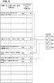
Fig. 2 is an image diagram showing one specific example in which theterminal allocating section 23 sets allocation of the input terminal 11 to thefunction input terminal 21. - The
Motor control device 100 can perform a plurality of functions. Examples of thefunction input terminal 21 include "reverse direction driving inhibition input", "forward direction operation command input", "compulsive brake locking input", "direct current braking command input", "operation command switching input", and "frequency command switching input". Individualfunction input terminal 21 listed here are briefly described below. - "Reverse direction driving inhibition input": the
function input terminal 21 that prevents themotor 101 from driving in a reverse direction
"Forward direction operation command input": thefunction input terminal 21 corresponding to the function of operating themotor 101 in a forward direction
"Compulsive brake locking input": thefunction input terminal 21 corresponding to the function of compulsively operating a brake which physically stops rotation of themotor 101
"Direct current braking command input": thefunction input terminal 21 corresponding to the function of electrically stopping rotation of themotor 101
"Operation command switching input": thefunction input terminal 21 corresponding to the function of selecting a path of a command for operation of the motor control device 100 (communication from the master device/signal input to the input terminal 11)
"Frequency command switching input": thefunction input terminal 21 corresponding to the function of selecting a path to set frequency to the motor control device 100 (communication from the master device/signal input to the input terminal 11)
Theterminal allocating section 23 allocates a terminal IN1 as the input terminal 11 to "reverse direction driving inhibition input" and "forward direction operation command input". Consequently, in response to a signal supplied from the terminal IN1 to themain MPU 2, themain MPU 2 operates themotor 101 in the forward direction while preventing themotor 101 from being driven in the reverse direction, so that themotor 101 can be operated in the forward direction more reliably. - The
terminal allocating section 23 allocates a terminal IN2 as the input terminal 11 to "compulsive brake locking input" and "direct current braking command input". As a result, themain MPU 2 physically and electrically stops rotation of themotor 101 in response to a signal supplied from the terminal IN2 to themain MPU 2, so that the rotation ofmotor 101 can be stopped more reliably. - The
terminal allocating section 23 allocates a terminal IN3 as the input terminal 11 to "operation command switching input" and "frequency command switching input". This allows for switching between a remote operation in which the master device operates themotor control device 100 and a local operation in which the user operates themotor control device 100 using thecontrol tool 104. -
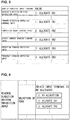
Fig. 3 is a table showing a specific example of the display content displayed by thedisplay section 1041 at the time of setting allocation of the input terminal 11 to thefunction input terminal 21. - In the
Fig. 3 table, the "name of function input terminal" column shows the name of eachfunction input terminal 21, as with the "name of function input terminal" column inFig. 2 . On the other hand, in theFig. 3 table, the "value" column shows a value indicating which input terminal 11 is allocated for eachfunction input terminal 21. By causing thedisplay section 1041 to display such a table, the user can visually check the setting of the allocation. -
Fig. 4 is a diagram showing an exemplary set parameter of thefunction input terminal 21. - According to
Fig. 4 , the set parameter of "reverse direction driving inhibition input" as thefunction input terminal 21 contains a parameter "selection of port". This parameter "selection of port" is set to either "0", which is a value indicating that the input terminal 11 is not allocated to the "reverse direction driving inhibition input", or "1", "2", ..., which is a value indicating that the input terminal 11 is allocated to the "reverse direction driving inhibition input". FromFig. 4 , it can be seen that whether or not the input terminal 11 is allocated to thefunction input terminal 21 can be checked and which of the plurality of input terminals 11 is to be allocated to thefunction input terminal 21 can be set. -
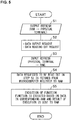
Fig. 5 is a flow chart illustrating an exemplary process flow in themain MPU 2 and its surrounding elements. - First, output refresh (RAM → physical terminal) is performed (step S1). The output refresh (RAM → physical terminal) is a process of outputting data on a RAM of the
main MPU 2 to a physical terminal of themain MPU 2. Here, the physical terminal is an output port on themain MPU 2, and corresponds to a process of outputting a signal to theoutput terminal 12 and the MCU 3 (microcomputer for controlling the motor 101). - Subsequently, a data output request and/or a data reading-out request are performed (step S2). That is, in the step S2, the
MCU 3 transmits data for output to themain MPU 2, and/or themain MPU 2 requests theMCU 3 to read out status information indicative of the status of themotor 101 or the like. - Subsequently, input refresh (physical terminal → RAM) is performed (step S3). The input refresh (physical terminal → RAM) is a process of extracting a signal state from the physical terminal of the
main MPU 2 and loading it in the RAM. Here, the physical terminal is an input port on themain MPU 2, and corresponds to a process of reading out data from the input terminal 11 and the MCU 3 (microcomputer for controlling the motor 101). - Subsequently, the
MCU 3 fetches, from a microcomputer register (not shown) of themain MPU 2 to the RAM (not shown), the data requested to be read out in the step S2 (step S4). - Subsequently, the
main MPU 2 executes the function based on the data in the corresponding RAM, and sends the result of the execution to the RAM (execution of function) (step S5). - It should be noted that an initial value at the time of turning on the power of the
motor control device 100 may be outputted until a first execution of a function in themotor control device 100 is performed. In addition, in the step S3, data is copied to the RAM in charge of the corresponding function based on the value set in the parameter "selection of port" inFig. 4 . -
Fig. 6 is an image diagram showing another specific example in which theterminal allocating section 23 sets allocation of the input terminal 11 to thefunction input terminal 21. - Examples of the
function input terminal 21 include "output block input (first function input terminal)" and "operation command switching input (second function input terminal)". Thefunction input terminals 21 listed here are briefly described below. - "Output block input": the
function input terminal 21 corresponding to the function of stopping outputting to themotor 101 and putting themotor 101 in a free run status. - "Operation command switching input": the
function input terminal 21 corresponding to the function of selecting a path of a command for operation of the motor control device 100 (communication from the master device/signal input to the input terminal 11)
Thetiming control section 24 causes the timing of supplying, to "output block input", the signal having been supplied to the terminal IN4 as the input terminal 11 to be different from the timing of supplying the signal to the "operation command switching input". -
Fig. 7 is a table showing another specific example of the display content displayed by thedisplay section 1041 at the time of setting the allocation of the input terminal 11 to thefunction input terminal 21. - In the
Fig. 7 table, the "name of function input terminal or delay timer" column shows the name of the parameter "delay timer" in addition to the name of eachfunction input terminal 21. On the other hand, in theFig. 7 table, the "value" column shows a value indicating which input terminal 11 is allocated for eachfunction input terminal 21. In addition, in theFig. 7 table, the "value" column shows a delay time (unit: ms (milliseconds)) indicative of how delayed, with respect to a reference time, the timing with which thetiming control section 24 supplies the signal having been supplied to the input terminal 11 to the correspondingfunction input terminal 21 is. -
Fig. 8 is a timing chart comparing a signal supplied to the input terminal 11 (terminal IN4), a signal supplied to the "output block input", and a signal supplied to the "operation command switching input". - The rising edge of the signal supplied to the "output block input" is delayed by 10ms with respect to the rising edge of the signal supplied to the terminal IN4. On the other hand, the rising edge of the signal supplied to the "operation command switching input" is delayed by 20ms with respect to the rising edge of the signal supplied to the terminal IN4. In other words, the rising edge of the signal supplied to the "operation command switching input" is delayed by 10ms with respect to the rising edge of the signal supplied to the "output block input". In this manner, the
timing control section 24 can cause the timing of supplying, to the "output block input", the signal having been supplied to the input terminal 11 (terminal IN4) to be different from the timing of supplying the signal to the "operation command switching input". -
Fig. 9 is a diagram showing an example of the display content which thedisplay output section 25 causes the display device to display. In the diagram shown inFig. 9 , a correspondence between the input terminal 11 and one of the plurality offunction input terminals 21 to which one the input terminal 11 has been allocated (corresponding to the checked one inFig. 9 ) is shown. Further, in the drawing shown inFig. 9 , a list in which this correspondence is shown is created in one tab, and such a tab is created for each of the plurality of input terminals 11, thereby forming one displayed content. Thedisplay output section 25 creates such a display content and causes the display device to display the display content. The display device may be thedisplay section 1041 or another display device. - Alternatively, the
display output section 25 may create the display content indicating the aforementioned correspondence in an image diagram of connection, and cause the display device to display the display content. Alternatively, thedisplay output section 25 may create, as the display content, a list of thefunction input terminal 21 allocated to the input terminal 11 based on this input terminal 11, and cause the display device to display the list. - Further, by enabling the checking of the display content related to
Fig. 9 , the display content related toFig. 9 may be a setting window itself for setting thefunction input terminal 21 to which the input terminal 11 is allocated. - In the
motor control device 100, according to the same principles as in theterminal allocating section 23, which of the plurality ofoutput terminals 12 is to be allocated to each of the plurality offunction output terminals 22 that are included in themain MPU 2 and that correspond to the plurality of functions in themotor control device 100 may be set according to selection by a user. In this case, themain MPU 2 may supply a logical disjunction (OR) of signals having been outputted from each of at least twofunction output terminals 22 to which thesame output terminal 12 has been allocated, to thatoutput terminal 12. Instead of the logical disjunction, an exclusive disjunction (EXOR), a logical conjunction (AND), a joint denial (NOR), or Sheffer stroke (NAND) may be applied, or a combination of two or more of these logical operations and negations (NOT) may be applied. - Control blocks of the motor control device 100 (particularly, the
terminal allocating section 23, thetiming control section 24, and the display output section 25) can be realized by a logic circuit (hardware) provided in an integrated circuit (IC chip) or the like or can be alternatively realized by software. - In the latter case, the
motor control device 100 includes a computer that executes instructions of a program that is software realizing the foregoing functions. The computer, for example, includes at least one processor and at least one computer-readable storage medium storing the program. An object of the present invention can be achieved by the processor of the computer reading and executing the program stored in the storage medium. Examples of the processor encompass a central processing unit (CPU). Examples of the storage medium encompass a "non-transitory tangible medium" such as a read only memory (ROM), a tape, a disk, a card, a semiconductor memory, and a programmable logic circuit. The computer may further include a random access memory (RAM) or the like in which the program is loaded. Further, the program may be made available to the computer via any transmission medium (such as a communication network and a broadcast wave) which allows the program to be transmitted. Note that an aspect of the present invention can also be achieved in the form of a computer data signal in which the program is embodied via electronic transmission and which is embedded in a carrier wave. - Aspects of the present invention can also be expressed as follows:
A motor control device in accordance with one aspect of the present invention comprises: a plurality of input terminals to which an input-side external device is connected; a plurality of function input terminals which are included in a main control section of the motor control device and which correspond to a plurality of functions of the motor control device, respectively; and a terminal allocating section for setting, in accordance with selection by a user, which of the plurality of input terminals is to be allocated to each of the plurality of function input terminals. - A method for controlling a motor control device in accordance with one aspect of the present invention is a method for controlling a motor control device including a plurality of input terminals to which an input-side external device is connected, said method comprising a terminal allocating step of setting, in accordance with selection by a user, which of the plurality of input terminal is to be allocated to each of a plurality of function input terminals which are included in a main control section of the motor control device and which correspond to a plurality of functions of the motor control device, respectively.
- With the arrangement, single input terminal can be allocated to at least two of the plurality of function input terminals, so that the number of the input terminals can be smaller than the number of the function input terminals. Accordingly, with the arrangement, it is possible to reduce the number of the input terminals. The reduction in the number of the input terminals leads to downsizing of the motor control device, a reduction in the number of wiring steps in the motor control device, and a reduction in the costs (manufacture cost and original cost) of the motor control device.
- Furthermore, with the arrangement, it is possible to allocate any number of function input terminals to one input terminal, as long as the performance of the motor control device allows. Therefore, flexibility of designing the motor control device can be improved as compared to the prior art.
- The motor control device in accordance with one aspect of the present invention is preferably arranged so as to further comprise a timing control section which, with respect to each of at least one of the plurality of input terminals, in accordance with selection by the user, causes timing of supplying a first function input terminal with a signal having been supplied to said at least one input terminal to be different from timing of supplying a second function input terminal with the signal, the first function input terminal and the second function input terminal being included in the plurality of function input terminals and being different from each other.
- With the arrangement, it is possible to supply a signal to the first function input terminal and the second function input terminal at different timings. Therefore, for example, this is convenient for executing a function corresponding to the second function input terminal some time after executing a function corresponding to the first function input terminal.
- The motor control device in accordance with one aspect of the present invention is preferably arranged so as to further comprise a display output section which, with respect to each of at least one of the plurality of input terminals, causes a display device to display correspondence between said at least one input terminal and one of the plurality of function input terminals to which one said at least one input terminal has been allocated.
- With the arrangement, a user can check a correspondence between the input terminal and one of the plurality of function input terminals to which one the input terminal has been allocated. Therefore, the user can check if the correspondence is different from one intended by the user or if the correspondence itself is inappropriate.
- The method for controlling the motor control device in accordance with one aspect of the present invention may be executed by a computer. In this case, a control program for causing a computer to execute the method for controlling the motor control device and a computer-readable storage medium in which the control program is stored are also encompassed in the scope of the present invention.
- The present invention is not limited to the embodiments, but can be altered by a skilled person in the art within the scope of the claims. The present invention also encompasses, in its technical scope, any embodiment derived by combining technical means disclosed in differing embodiments. Reference Signs List
-
- 1
- Connector
- 2
- Main MPU (main control section)
- 3
- MCU
- 4
- ASIC
- 5
- Interface
- 11
- Input terminal
- 12
- Output terminal
- 21
- Function input terminal
- 22
- Function output terminal
- 23
- Terminal allocating section
- 24
- Timing control section
- 25
- Display output section
- 100
- Motor control device
- 101
- Motor
- 102
- Input-side external device
- 103
- Output-side external device
- 104
- Control tool
- 1041
- Display section
Claims (6)
- A motor control device, comprising:a plurality of input terminals to which an input-side external device is connected;a plurality of function input terminals which are included in a main control section of the motor control device and which correspond to a plurality of functions of the motor control device, respectively; anda terminal allocating section for setting, in accordance with selection by a user, which of the plurality of input terminals is to be allocated to each of the plurality of function input terminals.
- The motor control device as set forth in claim 1, further comprising a timing control section which, with respect to each of at least one of the plurality of input terminals, in accordance with selection by the user, causes timing of supplying a first function input terminal with a signal having been supplied to said at least one input terminal to be different from timing of supplying a second function input terminal with the signal, the first function input terminal and the second function input terminal being included in the plurality of function input terminals and being different from each other.
- The motor control device as set forth in claim 1 or 2, further comprising a display output section which, with respect to each of at least one of the plurality of input terminals, causes a display device to display correspondence between said at least one input terminal and one of the plurality of function input terminals to which one said at least one input terminal has been allocated.
- A method for controlling a motor control device including a plurality of input terminals to which an input-side external device is connected,
said method comprising a terminal allocating step of setting, in accordance with selection by a user, which of the plurality of input terminal is to be allocated to each of a plurality of function input terminals which are included in a main control section of the motor control device and which correspond to a plurality of functions of the motor control device, respectively. - A control program for causing a computer to carry out a method for controlling a motor control device as set forth in claim 4.
- A computer-readable storage medium in which a control program as set forth in claim 5 is stored.
Applications Claiming Priority (2)
| Application Number | Priority Date | Filing Date | Title |
|---|---|---|---|
| JP2017230926A JP6939482B2 (en) | 2017-11-30 | 2017-11-30 | Motor control device, control method of motor control device, control program, and recording medium |
| PCT/JP2018/039752 WO2019107030A1 (en) | 2017-11-30 | 2018-10-25 | Motor control device, control method for motor control device, control program, and recording medium |
Publications (3)
| Publication Number | Publication Date |
|---|---|
| EP3719992A1 true EP3719992A1 (en) | 2020-10-07 |
| EP3719992A4 EP3719992A4 (en) | 2021-08-25 |
| EP3719992B1 EP3719992B1 (en) | 2025-07-30 |
Family
ID=66665551
Family Applications (1)
| Application Number | Title | Priority Date | Filing Date |
|---|---|---|---|
| EP18883628.2A Active EP3719992B1 (en) | 2017-11-30 | 2018-10-25 | Motor control device and control method for motor control device |
Country Status (5)
| Country | Link |
|---|---|
| US (1) | US11114973B2 (en) |
| EP (1) | EP3719992B1 (en) |
| JP (1) | JP6939482B2 (en) |
| CN (1) | CN111095780B (en) |
| WO (1) | WO2019107030A1 (en) |
Families Citing this family (1)
| Publication number | Priority date | Publication date | Assignee | Title |
|---|---|---|---|---|
| DE102020210555A1 (en) | 2020-08-20 | 2022-02-24 | Robert Bosch Gesellschaft mit beschränkter Haftung | Device and method for saving analog inputs on a control unit |
Family Cites Families (9)
| Publication number | Priority date | Publication date | Assignee | Title |
|---|---|---|---|---|
| US4284943A (en) * | 1979-02-13 | 1981-08-18 | Electric Machinery Mfg. Company | Apparatus and method for controlling the speed of an induction motor in a closed-loop system |
| JP3654930B2 (en) * | 1994-08-01 | 2005-06-02 | 株式会社東芝 | Inverter device |
| JPH0993987A (en) | 1995-09-28 | 1997-04-04 | Toshiba Corp | Inverter device |
| JP3499497B2 (en) * | 2000-03-31 | 2004-02-23 | 株式会社デジタル | Method and apparatus for setting parameters of motor control device |
| JP2008131671A (en) * | 2006-11-16 | 2008-06-05 | Yaskawa Electric Corp | Driving interlock processing circuit, motor control device, and control method of motor control device |
| CN101355334B (en) * | 2007-07-27 | 2010-11-03 | 比亚迪股份有限公司 | Control method for correcting phase of brushless DC motor without position sensor |
| CN102025312B (en) * | 2009-09-16 | 2014-01-29 | 株式会社东芝 | Motor control device and electrical equipment |
| CN102158157B (en) * | 2010-02-12 | 2013-07-31 | 深圳兴奇宏科技有限公司 | Method for automatically compensating phase current of motor |
| WO2013057767A1 (en) * | 2011-10-20 | 2013-04-25 | 株式会社協和製作所 | Motor drive device and roller conveyer device utilizing same |
-
2017
- 2017-11-30 JP JP2017230926A patent/JP6939482B2/en not_active Expired - Fee Related
-
2018
- 2018-10-25 WO PCT/JP2018/039752 patent/WO2019107030A1/en not_active Ceased
- 2018-10-25 US US16/644,979 patent/US11114973B2/en not_active Expired - Fee Related
- 2018-10-25 CN CN201880056298.4A patent/CN111095780B/en not_active Expired - Fee Related
- 2018-10-25 EP EP18883628.2A patent/EP3719992B1/en active Active
Also Published As
| Publication number | Publication date |
|---|---|
| US20200287500A1 (en) | 2020-09-10 |
| JP2019103222A (en) | 2019-06-24 |
| WO2019107030A1 (en) | 2019-06-06 |
| EP3719992A4 (en) | 2021-08-25 |
| JP6939482B2 (en) | 2021-09-22 |
| CN111095780A (en) | 2020-05-01 |
| EP3719992B1 (en) | 2025-07-30 |
| CN111095780B (en) | 2023-05-09 |
| US11114973B2 (en) | 2021-09-07 |
Similar Documents
| Publication | Publication Date | Title |
|---|---|---|
| EP3571585B1 (en) | Method and apparatus for implementing heterogeneous frequency operation and scheduling task of heterogeneous frequency cpu | |
| JP5500741B2 (en) | Interrupt approval in data processing systems | |
| US7650274B2 (en) | Microcomputer logic development system | |
| US7213084B2 (en) | System and method for allocating memory allocation bandwidth by assigning fixed priority of access to DMA machines and programmable priority to processing unit | |
| US10417153B2 (en) | Vehicle safety electronic control system | |
| EP3030971B1 (en) | Devices, systems, and methods of reducing chip select | |
| JP2010282617A5 (en) | ||
| EP3719992B1 (en) | Motor control device and control method for motor control device | |
| US5596749A (en) | Arbitration request sequencer | |
| CN107743621B (en) | IC input and output | |
| JP2008532147A (en) | Control device with configurable hardware module | |
| US12112206B2 (en) | Control device for controlling multiple applications based on priority-based message encryption arbitration | |
| EP4089541B1 (en) | System and method for controlling access to shared resource in system-on-chips | |
| EP2081093A2 (en) | Vehicle control apparatus | |
| US11086666B2 (en) | Activating tasks in an operating system using activation schemata | |
| EP2996044A1 (en) | Method for allocating an operating mode to a communication device | |
| US6848016B2 (en) | System and method for efficiently implementing an electronic device architecture | |
| EP3258371A1 (en) | Communication regulation in computing systems | |
| JP4620880B2 (en) | Semiconductor device and data transfer method | |
| US7043590B2 (en) | Interface apparatus using single driver, computer system including interface apparatus using single driver, and related method | |
| US10089156B2 (en) | Electronic device for synchronizing tasks of an electronic appliance | |
| CN106711960A (en) | Relay protection configuration method and relay protection system | |
| CN115079807A (en) | Communication device, memory access method of communication device and electronic equipment | |
| CN118400838A (en) | Synchronous flashing circuit of network port indicator lamp and control method | |
| CN116820241A (en) | Vibration control method and device, readable storage medium and electronic equipment |
Legal Events
| Date | Code | Title | Description |
|---|---|---|---|
| STAA | Information on the status of an ep patent application or granted ep patent |
Free format text: STATUS: THE INTERNATIONAL PUBLICATION HAS BEEN MADE |
|
| PUAI | Public reference made under article 153(3) epc to a published international application that has entered the european phase |
Free format text: ORIGINAL CODE: 0009012 |
|
| STAA | Information on the status of an ep patent application or granted ep patent |
Free format text: STATUS: REQUEST FOR EXAMINATION WAS MADE |
|
| 17P | Request for examination filed |
Effective date: 20200305 |
|
| AK | Designated contracting states |
Kind code of ref document: A1 Designated state(s): AL AT BE BG CH CY CZ DE DK EE ES FI FR GB GR HR HU IE IS IT LI LT LU LV MC MK MT NL NO PL PT RO RS SE SI SK SM TR |
|
| AX | Request for extension of the european patent |
Extension state: BA ME |
|
| DAV | Request for validation of the european patent (deleted) | ||
| DAX | Request for extension of the european patent (deleted) | ||
| A4 | Supplementary search report drawn up and despatched |
Effective date: 20210723 |
|
| RIC1 | Information provided on ipc code assigned before grant |
Ipc: H02P 29/00 20160101AFI20210719BHEP Ipc: H01R 29/00 20060101ALN20210719BHEP |
|
| STAA | Information on the status of an ep patent application or granted ep patent |
Free format text: STATUS: EXAMINATION IS IN PROGRESS |
|
| 17Q | First examination report despatched |
Effective date: 20230704 |
|
| GRAP | Despatch of communication of intention to grant a patent |
Free format text: ORIGINAL CODE: EPIDOSNIGR1 |
|
| STAA | Information on the status of an ep patent application or granted ep patent |
Free format text: STATUS: GRANT OF PATENT IS INTENDED |
|
| RIC1 | Information provided on ipc code assigned before grant |
Ipc: H01R 29/00 20060101ALN20250128BHEP Ipc: H02P 27/04 20160101ALI20250128BHEP Ipc: H02P 29/00 20160101AFI20250128BHEP |
|
| RIC1 | Information provided on ipc code assigned before grant |
Ipc: H01R 29/00 20060101ALN20250213BHEP Ipc: H02P 27/04 20160101ALI20250213BHEP Ipc: H02P 29/00 20160101AFI20250213BHEP |
|
| INTG | Intention to grant announced |
Effective date: 20250303 |
|
| GRAS | Grant fee paid |
Free format text: ORIGINAL CODE: EPIDOSNIGR3 |
|
| GRAA | (expected) grant |
Free format text: ORIGINAL CODE: 0009210 |
|
| STAA | Information on the status of an ep patent application or granted ep patent |
Free format text: STATUS: THE PATENT HAS BEEN GRANTED |
|
| AK | Designated contracting states |
Kind code of ref document: B1 Designated state(s): AL AT BE BG CH CY CZ DE DK EE ES FI FR GB GR HR HU IE IS IT LI LT LU LV MC MK MT NL NO PL PT RO RS SE SI SK SM TR |
|
| REG | Reference to a national code |
Ref country code: GB Ref legal event code: FG4D |
|
| REG | Reference to a national code |
Ref country code: CH Ref legal event code: EP |
|
| REG | Reference to a national code |
Ref country code: DE Ref legal event code: R096 Ref document number: 602018084177 Country of ref document: DE |
|
| REG | Reference to a national code |
Ref country code: IE Ref legal event code: FG4D |
|
| REG | Reference to a national code |
Ref country code: NL Ref legal event code: MP Effective date: 20250730 |
|
| REG | Reference to a national code |
Ref country code: AT Ref legal event code: MK05 Ref document number: 1820133 Country of ref document: AT Kind code of ref document: T Effective date: 20250730 |
|
| PG25 | Lapsed in a contracting state [announced via postgrant information from national office to epo] |
Ref country code: PT Free format text: LAPSE BECAUSE OF FAILURE TO SUBMIT A TRANSLATION OF THE DESCRIPTION OR TO PAY THE FEE WITHIN THE PRESCRIBED TIME-LIMIT Effective date: 20251202 |
|
| PG25 | Lapsed in a contracting state [announced via postgrant information from national office to epo] |
Ref country code: IS Free format text: LAPSE BECAUSE OF FAILURE TO SUBMIT A TRANSLATION OF THE DESCRIPTION OR TO PAY THE FEE WITHIN THE PRESCRIBED TIME-LIMIT Effective date: 20251130 |
|
| PG25 | Lapsed in a contracting state [announced via postgrant information from national office to epo] |
Ref country code: NO Free format text: LAPSE BECAUSE OF FAILURE TO SUBMIT A TRANSLATION OF THE DESCRIPTION OR TO PAY THE FEE WITHIN THE PRESCRIBED TIME-LIMIT Effective date: 20251030 |
|
| REG | Reference to a national code |
Ref country code: LT Ref legal event code: MG9D |
|
| PG25 | Lapsed in a contracting state [announced via postgrant information from national office to epo] |
Ref country code: AT Free format text: LAPSE BECAUSE OF FAILURE TO SUBMIT A TRANSLATION OF THE DESCRIPTION OR TO PAY THE FEE WITHIN THE PRESCRIBED TIME-LIMIT Effective date: 20250730 |
|
| PG25 | Lapsed in a contracting state [announced via postgrant information from national office to epo] |
Ref country code: FI Free format text: LAPSE BECAUSE OF FAILURE TO SUBMIT A TRANSLATION OF THE DESCRIPTION OR TO PAY THE FEE WITHIN THE PRESCRIBED TIME-LIMIT Effective date: 20250730 |
|
| PG25 | Lapsed in a contracting state [announced via postgrant information from national office to epo] |
Ref country code: HR Free format text: LAPSE BECAUSE OF FAILURE TO SUBMIT A TRANSLATION OF THE DESCRIPTION OR TO PAY THE FEE WITHIN THE PRESCRIBED TIME-LIMIT Effective date: 20250730 Ref country code: NL Free format text: LAPSE BECAUSE OF FAILURE TO SUBMIT A TRANSLATION OF THE DESCRIPTION OR TO PAY THE FEE WITHIN THE PRESCRIBED TIME-LIMIT Effective date: 20250730 |
|
| PG25 | Lapsed in a contracting state [announced via postgrant information from national office to epo] |
Ref country code: GR Free format text: LAPSE BECAUSE OF FAILURE TO SUBMIT A TRANSLATION OF THE DESCRIPTION OR TO PAY THE FEE WITHIN THE PRESCRIBED TIME-LIMIT Effective date: 20251031 |
|
| PG25 | Lapsed in a contracting state [announced via postgrant information from national office to epo] |
Ref country code: SE Free format text: LAPSE BECAUSE OF FAILURE TO SUBMIT A TRANSLATION OF THE DESCRIPTION OR TO PAY THE FEE WITHIN THE PRESCRIBED TIME-LIMIT Effective date: 20250730 |
|
| PG25 | Lapsed in a contracting state [announced via postgrant information from national office to epo] |
Ref country code: LV Free format text: LAPSE BECAUSE OF FAILURE TO SUBMIT A TRANSLATION OF THE DESCRIPTION OR TO PAY THE FEE WITHIN THE PRESCRIBED TIME-LIMIT Effective date: 20250730 |
|
| PG25 | Lapsed in a contracting state [announced via postgrant information from national office to epo] |
Ref country code: PL Free format text: LAPSE BECAUSE OF FAILURE TO SUBMIT A TRANSLATION OF THE DESCRIPTION OR TO PAY THE FEE WITHIN THE PRESCRIBED TIME-LIMIT Effective date: 20250730 Ref country code: BG Free format text: LAPSE BECAUSE OF FAILURE TO SUBMIT A TRANSLATION OF THE DESCRIPTION OR TO PAY THE FEE WITHIN THE PRESCRIBED TIME-LIMIT Effective date: 20250730 |
|
| PG25 | Lapsed in a contracting state [announced via postgrant information from national office to epo] |
Ref country code: RS Free format text: LAPSE BECAUSE OF FAILURE TO SUBMIT A TRANSLATION OF THE DESCRIPTION OR TO PAY THE FEE WITHIN THE PRESCRIBED TIME-LIMIT Effective date: 20251030 |
|
| PG25 | Lapsed in a contracting state [announced via postgrant information from national office to epo] |
Ref country code: ES Free format text: LAPSE BECAUSE OF FAILURE TO SUBMIT A TRANSLATION OF THE DESCRIPTION OR TO PAY THE FEE WITHIN THE PRESCRIBED TIME-LIMIT Effective date: 20250730 |
|
| PG25 | Lapsed in a contracting state [announced via postgrant information from national office to epo] |
Ref country code: RO Free format text: LAPSE BECAUSE OF FAILURE TO SUBMIT A TRANSLATION OF THE DESCRIPTION OR TO PAY THE FEE WITHIN THE PRESCRIBED TIME-LIMIT Effective date: 20250730 |
|
| PG25 | Lapsed in a contracting state [announced via postgrant information from national office to epo] |
Ref country code: SM Free format text: LAPSE BECAUSE OF FAILURE TO SUBMIT A TRANSLATION OF THE DESCRIPTION OR TO PAY THE FEE WITHIN THE PRESCRIBED TIME-LIMIT Effective date: 20250730 |
|
| PG25 | Lapsed in a contracting state [announced via postgrant information from national office to epo] |
Ref country code: DK Free format text: LAPSE BECAUSE OF FAILURE TO SUBMIT A TRANSLATION OF THE DESCRIPTION OR TO PAY THE FEE WITHIN THE PRESCRIBED TIME-LIMIT Effective date: 20250730 |
|
| PG25 | Lapsed in a contracting state [announced via postgrant information from national office to epo] |
Ref country code: IT Free format text: LAPSE BECAUSE OF FAILURE TO SUBMIT A TRANSLATION OF THE DESCRIPTION OR TO PAY THE FEE WITHIN THE PRESCRIBED TIME-LIMIT Effective date: 20250730 |
|
| PG25 | Lapsed in a contracting state [announced via postgrant information from national office to epo] |
Ref country code: CZ Free format text: LAPSE BECAUSE OF FAILURE TO SUBMIT A TRANSLATION OF THE DESCRIPTION OR TO PAY THE FEE WITHIN THE PRESCRIBED TIME-LIMIT Effective date: 20250730 |
|
| PG25 | Lapsed in a contracting state [announced via postgrant information from national office to epo] |
Ref country code: SK Free format text: LAPSE BECAUSE OF FAILURE TO SUBMIT A TRANSLATION OF THE DESCRIPTION OR TO PAY THE FEE WITHIN THE PRESCRIBED TIME-LIMIT Effective date: 20250730 Ref country code: EE Free format text: LAPSE BECAUSE OF FAILURE TO SUBMIT A TRANSLATION OF THE DESCRIPTION OR TO PAY THE FEE WITHIN THE PRESCRIBED TIME-LIMIT Effective date: 20250730 |
|
| REG | Reference to a national code |
Ref country code: DE Ref legal event code: R119 Ref document number: 602018084177 Country of ref document: DE |
|
| REG | Reference to a national code |
Ref country code: CH Ref legal event code: H13 Free format text: ST27 STATUS EVENT CODE: U-0-0-H10-H13 (AS PROVIDED BY THE NATIONAL OFFICE) Effective date: 20260527 |
|
| PLBE | No opposition filed within time limit |
Free format text: ORIGINAL CODE: 0009261 |
|
| STAA | Information on the status of an ep patent application or granted ep patent |
Free format text: STATUS: NO OPPOSITION FILED WITHIN TIME LIMIT |
|
| REG | Reference to a national code |
Ref country code: CH Ref legal event code: L10 Free format text: ST27 STATUS EVENT CODE: U-0-0-L10-L00 (AS PROVIDED BY THE NATIONAL OFFICE) Effective date: 20260611 |
|
| PG25 | Lapsed in a contracting state [announced via postgrant information from national office to epo] |
Ref country code: LU Free format text: LAPSE BECAUSE OF NON-PAYMENT OF DUE FEES Effective date: 20251025 |
|
| REG | Reference to a national code |
Ref country code: BE Ref legal event code: MM Effective date: 20251031 |
|
| GBPC | Gb: european patent ceased through non-payment of renewal fee |
Effective date: 20251030 |
|
| PG25 | Lapsed in a contracting state [announced via postgrant information from national office to epo] |
Ref country code: MC Free format text: LAPSE BECAUSE OF FAILURE TO SUBMIT A TRANSLATION OF THE DESCRIPTION OR TO PAY THE FEE WITHIN THE PRESCRIBED TIME-LIMIT Effective date: 20250730 Ref country code: LT Free format text: LAPSE BECAUSE OF FAILURE TO SUBMIT A TRANSLATION OF THE DESCRIPTION OR TO PAY THE FEE WITHIN THE PRESCRIBED TIME-LIMIT Effective date: 20250730 |
|
| 26N | No opposition filed |
Effective date: 20260501 |
|
| PG25 | Lapsed in a contracting state [announced via postgrant information from national office to epo] |
Ref country code: GB Free format text: LAPSE BECAUSE OF NON-PAYMENT OF DUE FEES Effective date: 20251030 |
|
| PG25 | Lapsed in a contracting state [announced via postgrant information from national office to epo] |
Ref country code: DE Free format text: LAPSE BECAUSE OF NON-PAYMENT OF DUE FEES Effective date: 20260501 |
|
| PG25 | Lapsed in a contracting state [announced via postgrant information from national office to epo] |
Ref country code: BE Free format text: LAPSE BECAUSE OF NON-PAYMENT OF DUE FEES Effective date: 20251031 Ref country code: CH Free format text: LAPSE BECAUSE OF NON-PAYMENT OF DUE FEES Effective date: 20251031 |
|
| PG25 | Lapsed in a contracting state [announced via postgrant information from national office to epo] |
Ref country code: FR Free format text: LAPSE BECAUSE OF NON-PAYMENT OF DUE FEES Effective date: 20251031 |