EP3719859A1 - Display panel, packaging method therefor, and display device - Google Patents
Display panel, packaging method therefor, and display device Download PDFInfo
- Publication number
- EP3719859A1 EP3719859A1 EP18859942.7A EP18859942A EP3719859A1 EP 3719859 A1 EP3719859 A1 EP 3719859A1 EP 18859942 A EP18859942 A EP 18859942A EP 3719859 A1 EP3719859 A1 EP 3719859A1
- Authority
- EP
- European Patent Office
- Prior art keywords
- film
- inorganic film
- region
- display
- organic
- Prior art date
- Legal status (The legal status is an assumption and is not a legal conclusion. Google has not performed a legal analysis and makes no representation as to the accuracy of the status listed.)
- Granted
Links
Images

Classifications
-
- H—ELECTRICITY
- H10—SEMICONDUCTOR DEVICES; ELECTRIC SOLID-STATE DEVICES NOT OTHERWISE PROVIDED FOR
- H10K—ORGANIC ELECTRIC SOLID-STATE DEVICES
- H10K59/00—Integrated devices, or assemblies of multiple devices, comprising at least one organic light-emitting element covered by group H10K50/00
- H10K59/80—Constructional details
- H10K59/87—Passivation; Containers; Encapsulations
- H10K59/873—Encapsulations
- H10K59/8731—Encapsulations multilayered coatings having a repetitive structure, e.g. having multiple organic-inorganic bilayers
-
- H—ELECTRICITY
- H10—SEMICONDUCTOR DEVICES; ELECTRIC SOLID-STATE DEVICES NOT OTHERWISE PROVIDED FOR
- H10K—ORGANIC ELECTRIC SOLID-STATE DEVICES
- H10K50/00—Organic light-emitting devices
- H10K50/80—Constructional details
- H10K50/84—Passivation; Containers; Encapsulations
- H10K50/844—Encapsulations
-
- H—ELECTRICITY
- H10—SEMICONDUCTOR DEVICES; ELECTRIC SOLID-STATE DEVICES NOT OTHERWISE PROVIDED FOR
- H10K—ORGANIC ELECTRIC SOLID-STATE DEVICES
- H10K71/00—Manufacture or treatment specially adapted for the organic devices covered by this subclass
Definitions
- the present disclosure relates to the field of display technology, in particular to a display panel and a method for packaging the same, and a display device comprising the display panel.
- the package film layer of the existing flexible OLED package structure comprises an organic film and an inorganic film laminated in sequence.
- the organic film is formed by inkjet printing a rheological organic material, such as an acrylic material, in a filled region surrounded by a barrier and then making the rheological organic material solidify in the filled region.
- a display panel comprising a display substrate and at least one package film layer covering the display substrate, wherein the package film layer comprises a first inorganic film, a second inorganic film, an organic film and a third inorganic film laminated on the display substrate in sequence, and wherein an adhesion between a material of the first inorganic film and a material of the organic film is less than an adhesion between a material of the second inorganic film and a material of the organic film.
- the display panel comprises a display region and a non-display region, the non-display region comprising a first region provided with a barrier structure and a second region between the display region and the barrier structure, the first inorganic film covering the second region and the barrier structure, and the second inorganic film and the organic film cover the second region but not cover the barrier structure.
- the third inorganic film covers the second region and the barrier structure.
- the third inorganic film and the first inorganic film are made of a same material.
- the at least one package film layer comprises two package film layers.
- the two package film layers comprises a first package film layer and a second package film layer laminated in sequence
- the third inorganic film of the first package film layer is reused as the first inorganic film of the second package film layer.
- the first inorganic film is made of silicon nitride
- the second inorganic film is made of silicon oxynitride
- the third inorganic film is made of silicon nitride.
- the first inorganic film has a thickness of 500 nm to 1000 nm
- the second inorganic film has a thickness of 50 nm to 100 nm
- the third inorganic film has a thickness of 500 nm to 1000 nm.
- the barrier structure comprises at least a first barrier and a second barrier, a distance between the first barrier and the display region is less than a distance between the second barrier and the display region, and a height of the first barrier is less than a height of the second barrier.
- the display substrate is an Organic Light-Emitting Diode (OLED) display substrate.
- OLED Organic Light-Emitting Diode
- An embodiment of the present disclosure further provides a display device including the display panel as described above.
- An embodiment of the present disclosure further provides a method for packaging a display panel, comprising forming at least one package film layer on a display substrate for covering the display substrate, wherein a step of forming the package film layer comprises: laminating a first inorganic film, a second inorganic film, an organic film and a third inorganic film on the display substrate in sequence, wherein an adhesion between a material of the first inorganic film and a material of the organic film is less than an adhesion between a material of the second inorganic film and a material of the organic film.
- the display panel comprises a display region and a non-display region, the non-display region comprising a first region provided with a barrier structure and a second region between the display region and the barrier structure
- the method for packaging comprises:
- the packaging process of the related flexible OLED package structure mainly comprises: manufacturing a flexible substrate; manufacturing a first gate insulating layer; manufacturing a first gate metal layer pattern; manufacturing a second gate insulating layer; manufacturing a second gate metal layer pattern; manufacturing an interlayer insulating layer; manufacturing the source-drain metal layer pattern; manufacturing an overcoat; manufacturing an anode; manufacturing a pixel defining layer; manufacturing a spacer layer; manufacturing a cathode; manufacturing a package film layer.
- the package film layer comprises an organic film and an inorganic film laminated in sequence.
- an organic film is formed by inkjet printing a rheological organic material, such as an acrylic material, in a filled region surrounded by a barrier and making the rheological organic material in the filled region solidifying.
- the package film layer needs to concern both the high water-oxygen barrier capacity and the uniformity of the organic film.
- the related package film layer cannot concern both the high water-oxygen barrier capacity and the uniformity of the organic film.
- the package film layer may be a laminated structure of an inorganic film / an organic film / an inorganic film.
- the inorganic film may be made by various common film forming methods. Alternatively, the film is formed by CVD (Chemical Vapor Deposition) process, and the inorganic film (silicon nitride layer or silicon oxynitride layer) formed by CVD process has strong water-oxygen barrier capacity, good light transmittance and good wear resistance.
- silicon nitride for example, SiNx
- silicon oxynitride for example, SiON
- silicon nitride has a better water-oxygen barrier capacity, but has a relatively poor adhesion to the material of the organic film
- silicon oxynitride has a relatively poor water-oxygen barrier capacity, but has a better adhesion to the material of the organic film and allows the organic ink to have a better fluidity.
- a silicon nitride layer / organic film / silicon nitride layer is used as the package film layer, the uniformity of the organic film will be relatively poor, because the rheological organic material has a relatively poor leveling diffusion property on the surface of silicon nitride layer. As shown in Fig.
- the water-oxygen barrier capacity of the entire package film layer is relatively poor, because the silicon oxynitride layer 12 has a relatively poor water-oxygen barrier capacity; and, the climbing distance D of the organic film 13 is relatively large, which is not conducive to achieving a narrow bezel of the display device, because the rheological organic material has a relatively good leveling diffusion property on the surface of silicon nitride layer.
- the above-mentioned package film layer cannot concern both the high water-oxygen barrier capacity and the uniformity of the organic film.
- embodiments of the present disclosure provide a display panel and a display device comprising the display panel, which are capable of concerning both the high water-oxygen barrier capacity and the uniformity of the organic film.
- An embodiment of the present disclosure provides a display panel, as shown in Fig. 2 , comprising a display substrate and at least one package film layer covering the display substrate, the package film layer comprising a first inorganic film 3, a second inorganic film 4, an organic film 5 and a third inorganic film 6 laminated on the display substrate in sequence, wherein an adhesion between a material of the first inorganic film 3 to a material of the organic film 5 is less than an adhesion between a material of the second inorganic film 4 to a material of the organic film 5.
- the adhesion between the material of the first inorganic film and the material of the organic film is less than the adhesion between the material of the second inorganic film and the material of the organic film, when the rheological organic material is formed on the second inorganic film, the rheological organic material has a relatively good leveling diffusion property on the surface of the second inorganic film, thereby being capable of forming an organic film having relatively good uniformity.
- the adhesion between the material of the first inorganic film and the material of the organic film is relatively weak, it is ensured that the package film layer has a relatively good water-oxygen barrier capacity.
- the display panel comrpises a display region C and a non-display region, the non-display region including a first region A provided for a barrier structure and a second region B between the display region and the barrier structure.
- a device layer 2 on the base substrate 1 is provided in the second region B.
- the device layer 2 may, for example, comprises an anode layer and a cathode layer.
- the first inorganic film 3 covers the second region B and the barrier structure, and the second inorganic film 4 and the organic film 5 only cover the second region B but not cover the barrier structure.
- the first inorganic film 3 covers the second region B and the barrier structure, and the second inorganic film 4 and the organic film 5 cover the second region B but not covers the barrier structure
- the rheological organic material when the rheological organic material is leveled on the surface of the second inorganic film 4 and diffuses to the barrier structure, it is possible to prevent the rheological organic material from diffusing to the barrier structure, and confines the organic film 5 to the range defined by the barrier structure. This is because the adhesion between the material of the first inorganic film 3 covering the barrier structure and the material of the organic film 5 is relatively weak. Therefore, the rheological organic material, before passing over the barrier structure, solidifies to form the organic film 5, which contributes to realizing a narrow bezel of the display device.
- the constituent materials of the third inorganic film 6 and the first inorganic film 3 may be the same. That is, an adhesion between a material of the third inorganic film 6 to a material of the organic film 5 is less than an adhesion between a material of the second inorganic film 4 to a material of the organic film 5, or relatively weak.
- the third inorganic film 6 covers the second region B and the barrier structure. Since the adhesion between the material of the third inorganic film 6 to the material of the organic film 5 is relatively weak, and the inorganic film has a stronger water-oxygen barrier capacity compared with the organic film, the third inorganic film 6 covers the second region B and the barrier structure, which contributes to ensuring the water-oxygen barrier capacity of the package film layer.
- the at least one package film layer comprises a first package film layer and a second package film layer laminated in sequence
- the third inorganic film 6 of the first package film layer is reused as the first inorganic film 3 of the second package film layer.
- the first package film layer comprises a first inorganic film 3, a second inorganic film 4, an organic film 5, and a third inorganic film 6; and the second package film layer comprises a first inorganic film 3', and a second inorganic film 4', an organic film 5', and an third inorganic film 6', wherein the third inorganic film 6 of the first package film is reused as the first inorganic film 3' of the second package film layer, that is, the third inorganic film 6 is the same as the first inorganic film 3'.
- the package structure can minimize the thickness of the package film layer.
- the first inorganic film 3 has a thickness of 500 nm to 1000 nm
- the second inorganic film 4 has a thickness of 50 nm to 100 nm
- the third inorganic film 6 has a thickness of 500 nm to 1000 nm.
- the first inorganic film 3 is made of silicon nitride
- the second inorganic film 4 is made of silicon oxynitride
- the third inorganic film 6 is made of silicon nitride, that is, the package film layer has a structure of a silicon nitride film / a silicon oxynitride film / an organic film 5 / a silicon nitride film.
- the two layers of silicon nitride film are manufactured by process parameters with a high water resistance, and have a thickness of about 500 nm to 1000 nm; and the silicon oxynitride film is manufactured by process parameters with a good diffusion capacity, and has a thickness of about 50 nm to 100 nm.
- the thickness of the package film layer can be relatively small, and the package film layer can have a relatively good water-oxygen barrier capacity.
- the adhesion between the silicon nitride film and the organic film 5 is relatively poor, and the adhesion between the silicon oxynitride film and the organic film 5 is relatively good.
- the edge of the silicon oxynitride film is closely contact with the inside of the barrier 7 proximate to the display region, and the edge of the two silicon nitride films are designed to be outside of the barrier 7 in the outermost side.
- the rheological organic material When the rheological organic material is close to the barrier 7 proximate to the display region, due to the effect of the silicon nitride film, the climbing distance of the organic film 5 can be reduced, and finally the overall water-oxygen barrier capacity of the package film layer can be improved and the climb distance of the organic film can be reduced.
- the barrier structure comprises at least a first barrier 71 and a second barrier 72 separated by a predetermined distance, the distance between the first barrier 71 and the display region is less than a distance between the second barrier 72 and the display region, and a height of the first barrier 71 is less than a height of the second barrier 72.
- the first barrier 71 and the second barrier 72 are capable of forming a stepped structure, which better presents the rheological organic material from crossing the barrier structure.
- the display substrate is an OLED display substrate.
- the technical solution of the embodiment allows the OLED display panel to have a relatively good water-oxygen barrier capacity, and a relatively good uniformity of the organic film.
- An embodiment of the present disclosure further provides a display device comprising the display panel as described above.
- the display device may be any product or component having a display function, such as a television, a display, a digital photo frame, a mobile phone, a tablet computer, etc.
- the display device further comprises a flexible circuit board, a printed circuit board, and a backplane.
- the display device of the embodiment has a relatively good water-oxygen barrier capacity and a relatively good uniformity of the organic film, thereby ensuring the service life of the display device.
- the climbing distance of the organic film 5 is relatively short, so that the design distance between the edge of the display region and the barrier structure can be reduced, that is, the width of the second region B can be designed to be narrower, which contributes to a narrow bezel of the display device.
- An embodiment of the present disclosure further provides a method for packaging a display panel, comprising forming at least one package film layer on a display substrate for covering the display substrate, wherein the step of forming the package film layer comprises: laminating a first inorganic film 3, a second inorganic film 4, an organic film 5 and a first inorganic film 3 on the display substrate in sequence, wherein an adhesion between a material of the first inorganic film 3 to a material of the organic film 5 is less than an adhesion between a material of the second inorganic film 4 to a material of the organic film 5.
- the adhesion between the material of the first inorganic film and the material of the organic film is less than the adhesion between the material of the second inorganic film and the material of the organic film, when the rheological organic material is formed on the second inorganic film, it is capable of forming an organic film having relatively good uniformity. This is because the rheological diffusion property of the rheological organic material on the surface of the second inorganic film is relatively good. Moreover, since the adhesion between the material of the first inorganic film and the material of the organic film is relatively weak, it is ensured that the package film layer has a relatively good water-oxygen barrier capacity.
- the display panel comprises a display region and a non-display region, as shown in Fig. 2 , the non-display region comprising a first region A provided with a barrier structure and a second region B between the display region and the first region A.
- the method for packaging comprises:
- the rheological organic material may be printed on the second inorganic film 4.
- the rheological organic material When the rheological organic material is leveled on the surface of the second inorganic film 4 and diffuses to the barrier structure, since the adhesion between the material of the first inorganic film 3 covering the barrier structure and the material of the organic film 5 is relatively weak, it is possible to prevent the rheological organic material from diffusing to the barrier structure, thereby confining the organic film 5 to the range defined by the barrier structure. This contribute to solidifying the rheological organic material, before passing over the barrier structure, to form the organic film 5, which contributes to realizing a narrow bezel of the display device.
- the method for packaging the display panel of the embodiment specifically comprises the following steps:
- each of the package film layers comprises a silicon nitride film, a silicon oxynitride film, an organic film, and a silicon nitride film laminated in sequence. Since the adhesion between the silicon nitride film and the organic film is relatively weak and the adhesion between the silicon oxynitride film and the organic film is relatively good, when the rheological organic material is printed on the silicon oxynitride film, the rheological organic material has a relatively good leveling diffusion property on the surface of the silicon oxynitride film, thereby forming an organic film with a relatively good uniformity. Since the adhesion between the silicon nitride film and the organic film is relatively weak and the silicon nitride film has a relatively good water-oxygen barrier capacity, the package film layer can ensure a relatively good water-oxygen barrier capacity.
Landscapes
- Chemical & Material Sciences (AREA)
- Inorganic Chemistry (AREA)
- Physics & Mathematics (AREA)
- Optics & Photonics (AREA)
- Engineering & Computer Science (AREA)
- Manufacturing & Machinery (AREA)
- Electroluminescent Light Sources (AREA)
- Devices For Indicating Variable Information By Combining Individual Elements (AREA)
Abstract
Description
- This application claims a priority to Chinese Patent Application No.
201711240035.2 filed on November 30, 2017 - The present disclosure relates to the field of display technology, in particular to a display panel and a method for packaging the same, and a display device comprising the display panel.
- The development trends of Organic Light-Emitting Diode (OLED) display screens are narrow bezel, low power consumption, bendability, foldability and the like. The package film layer of the existing flexible OLED package structure comprises an organic film and an inorganic film laminated in sequence. In manufacturing the organic film, the organic film is formed by inkjet printing a rheological organic material, such as an acrylic material, in a filled region surrounded by a barrier and then making the rheological organic material solidify in the filled region.
- In an aspect, a display panel is provided, comprising a display substrate and at least one package film layer covering the display substrate, wherein the package film layer comprises a first inorganic film, a second inorganic film, an organic film and a third inorganic film laminated on the display substrate in sequence, and wherein an adhesion between a material of the first inorganic film and a material of the organic film is less than an adhesion between a material of the second inorganic film and a material of the organic film.
- Alternatively, the display panel comprises a display region and a non-display region, the non-display region comprising a first region provided with a barrier structure and a second region between the display region and the barrier structure, the first inorganic film covering the second region and the barrier structure, and the second inorganic film and the organic film cover the second region but not cover the barrier structure.
- Alternatively, the third inorganic film covers the second region and the barrier structure.
- Alternatively, the third inorganic film and the first inorganic film are made of a same material.
- Alternatively, the at least one package film layer comprises two package film layers.
- Alternatively, the two package film layers comprises a first package film layer and a second package film layer laminated in sequence, the third inorganic film of the first package film layer is reused as the first inorganic film of the second package film layer.
- Alternatively, the first inorganic film is made of silicon nitride, the second inorganic film is made of silicon oxynitride, and the third inorganic film is made of silicon nitride.
- Alternatively, the first inorganic film has a thickness of 500 nm to 1000 nm, the second inorganic film has a thickness of 50 nm to 100 nm, and the third inorganic film has a thickness of 500 nm to 1000 nm.
- Alternatively, the barrier structure comprises at least a first barrier and a second barrier, a distance between the first barrier and the display region is less than a distance between the second barrier and the display region, and a height of the first barrier is less than a height of the second barrier.
- Alternatively, the display substrate is an Organic Light-Emitting Diode (OLED) display substrate.
- An embodiment of the present disclosure further provides a display device including the display panel as described above.
- An embodiment of the present disclosure further provides a method for packaging a display panel, comprising forming at least one package film layer on a display substrate for covering the display substrate, wherein a step of forming the package film layer comprises:
laminating a first inorganic film, a second inorganic film, an organic film and a third inorganic film on the display substrate in sequence, wherein an adhesion between a material of the first inorganic film and a material of the organic film is less than an adhesion between a material of the second inorganic film and a material of the organic film. - Alternatively, the display panel comprises a display region and a non-display region, the non-display region comprising a first region provided with a barrier structure and a second region between the display region and the barrier structure, the method for packaging comprises:
- forming the first inorganic film covering the second region and the barrier structure;
- forming the second inorganic film covering the second region but not covering the barrier structure; and
- covering the second inorganic film with a rheological organic material, wherein the rheological organic material is blocked on a surface of the second inorganic film by the barrier structure and leveled to form the organic film, and the organic film covers the second region but not covers the barrier structure.
-
-
Fig. 1 is a schematic diagram of a related OLED display panel. -
Fig. 2 is a schematic diagram of a display panel according to an embodiment of the present disclosure. -
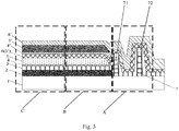
Fig. 3 is a schematic diagram of a display panel according to another embodiment of the present disclosure. - In order to make the technical problems to be solved, the technical solutions, and the advantages of the embodiments of the present disclosure, the present disclosure will be described hereinafter in conjunction with the drawings and specific examples.
- The development trends of OLED display screens are narrow bezel, low power consumption, bendability, foldability and the like. The packaging process of the related flexible OLED package structure mainly comprises: manufacturing a flexible substrate; manufacturing a first gate insulating layer; manufacturing a first gate metal layer pattern; manufacturing a second gate insulating layer; manufacturing a second gate metal layer pattern; manufacturing an interlayer insulating layer; manufacturing the source-drain metal layer pattern; manufacturing an overcoat; manufacturing an anode; manufacturing a pixel defining layer; manufacturing a spacer layer; manufacturing a cathode; manufacturing a package film layer. The package film layer comprises an organic film and an inorganic film laminated in sequence. In manufacturing the organic film, an organic film is formed by inkjet printing a rheological organic material, such as an acrylic material, in a filled region surrounded by a barrier and making the rheological organic material in the filled region solidifying.
- In order to ensure the display quality of the OLED display screen, the package film layer needs to concern both the high water-oxygen barrier capacity and the uniformity of the organic film. However, the related package film layer cannot concern both the high water-oxygen barrier capacity and the uniformity of the organic film.
- The package film layer may be a laminated structure of an inorganic film / an organic film / an inorganic film. The inorganic film may be made by various common film forming methods. Alternatively, the film is formed by CVD (Chemical Vapor Deposition) process, and the inorganic film (silicon nitride layer or silicon oxynitride layer) formed by CVD process has strong water-oxygen barrier capacity, good light transmittance and good wear resistance. Among silicon nitride (for example, SiNx) and silicon oxynitride (for example, SiON), silicon nitride has a better water-oxygen barrier capacity, but has a relatively poor adhesion to the material of the organic film; while silicon oxynitride has a relatively poor water-oxygen barrier capacity, but has a better adhesion to the material of the organic film and allows the organic ink to have a better fluidity. If a silicon nitride layer / organic film / silicon nitride layer is used as the package film layer, the uniformity of the organic film will be relatively poor, because the rheological organic material has a relatively poor leveling diffusion property on the surface of silicon nitride layer. As shown in
Fig. 1 , if thesilicon oxynitride layer 12 /organic film 13 /silicon nitride layer 15 is used as the package film layer, the water-oxygen barrier capacity of the entire package film layer is relatively poor, because thesilicon oxynitride layer 12 has a relatively poor water-oxygen barrier capacity; and, the climbing distance D of theorganic film 13 is relatively large, which is not conducive to achieving a narrow bezel of the display device, because the rheological organic material has a relatively good leveling diffusion property on the surface of silicon nitride layer. To sum up, the above-mentioned package film layer cannot concern both the high water-oxygen barrier capacity and the uniformity of the organic film. - In order to solve the above technical problems, embodiments of the present disclosure provide a display panel and a display device comprising the display panel, which are capable of concerning both the high water-oxygen barrier capacity and the uniformity of the organic film.
- An embodiment of the present disclosure provides a display panel, as shown in
Fig. 2 , comprising a display substrate and at least one package film layer covering the display substrate, the package film layer comprising a firstinorganic film 3, a second inorganic film 4, anorganic film 5 and a thirdinorganic film 6 laminated on the display substrate in sequence, wherein an adhesion between a material of the firstinorganic film 3 to a material of theorganic film 5 is less than an adhesion between a material of the second inorganic film 4 to a material of theorganic film 5. - In the present embodiment, since the adhesion between the material of the first inorganic film and the material of the organic film is less than the adhesion between the material of the second inorganic film and the material of the organic film, when the rheological organic material is formed on the second inorganic film, the rheological organic material has a relatively good leveling diffusion property on the surface of the second inorganic film, thereby being capable of forming an organic film having relatively good uniformity. Moreover, since the adhesion between the material of the first inorganic film and the material of the organic film is relatively weak, it is ensured that the package film layer has a relatively good water-oxygen barrier capacity.
- Alternatively, as shown in
Fig. 2 , the display panel comrpises a display region C and a non-display region, the non-display region including a first region A provided for a barrier structure and a second region B between the display region and the barrier structure. In the second region B, adevice layer 2 on the base substrate 1 is provided. Thedevice layer 2 may, for example, comprises an anode layer and a cathode layer. In the non-display region, the firstinorganic film 3 covers the second region B and the barrier structure, and the second inorganic film 4 and theorganic film 5 only cover the second region B but not cover the barrier structure. Since the firstinorganic film 3 covers the second region B and the barrier structure, and the second inorganic film 4 and theorganic film 5 cover the second region B but not covers the barrier structure, when the rheological organic material is leveled on the surface of the second inorganic film 4 and diffuses to the barrier structure, it is possible to prevent the rheological organic material from diffusing to the barrier structure, and confines theorganic film 5 to the range defined by the barrier structure. This is because the adhesion between the material of the firstinorganic film 3 covering the barrier structure and the material of theorganic film 5 is relatively weak. Therefore, the rheological organic material, before passing over the barrier structure, solidifies to form theorganic film 5, which contributes to realizing a narrow bezel of the display device. - In some embodiments, the constituent materials of the third
inorganic film 6 and the firstinorganic film 3 may be the same. That is, an adhesion between a material of the thirdinorganic film 6 to a material of theorganic film 5 is less than an adhesion between a material of the second inorganic film 4 to a material of theorganic film 5, or relatively weak. - Alternatively, as shown in
Fig. 2 , the thirdinorganic film 6 covers the second region B and the barrier structure. Since the adhesion between the material of the thirdinorganic film 6 to the material of theorganic film 5 is relatively weak, and the inorganic film has a stronger water-oxygen barrier capacity compared with the organic film, the thirdinorganic film 6 covers the second region B and the barrier structure, which contributes to ensuring the water-oxygen barrier capacity of the package film layer. - Alternatively, when the at least one package film layer comprises a first package film layer and a second package film layer laminated in sequence, the third
inorganic film 6 of the first package film layer is reused as the firstinorganic film 3 of the second package film layer. As shown inFig. 3 , the first package film layer comprises a firstinorganic film 3, a second inorganic film 4, anorganic film 5, and a thirdinorganic film 6; and the second package film layer comprises a first inorganic film 3', and a second inorganic film 4', an organic film 5', and an third inorganic film 6', wherein the thirdinorganic film 6 of the first package film is reused as the first inorganic film 3' of the second package film layer, that is, the thirdinorganic film 6 is the same as the first inorganic film 3'. The package structure can minimize the thickness of the package film layer. - Alternatively, the first
inorganic film 3 has a thickness of 500 nm to 1000 nm, the second inorganic film 4 has a thickness of 50 nm to 100 nm, and the thirdinorganic film 6 has a thickness of 500 nm to 1000 nm. - In an alternative embodiment, the first
inorganic film 3 is made of silicon nitride, the second inorganic film 4 is made of silicon oxynitride, and the thirdinorganic film 6 is made of silicon nitride, that is, the package film layer has a structure of a silicon nitride film / a silicon oxynitride film / anorganic film 5 / a silicon nitride film. The two layers of silicon nitride film are manufactured by process parameters with a high water resistance, and have a thickness of about 500 nm to 1000 nm; and the silicon oxynitride film is manufactured by process parameters with a good diffusion capacity, and has a thickness of about 50 nm to 100 nm. When the above parameters are used, the thickness of the package film layer can be relatively small, and the package film layer can have a relatively good water-oxygen barrier capacity. - In the package film layer, the adhesion between the silicon nitride film and the
organic film 5 is relatively poor, and the adhesion between the silicon oxynitride film and theorganic film 5 is relatively good. As shown inFig. 2 , the edge of the silicon oxynitride film is closely contact with the inside of thebarrier 7 proximate to the display region, and the edge of the two silicon nitride films are designed to be outside of thebarrier 7 in the outermost side. When the rheological organic material flows to the inside of thebarrier 7 proximate to the display region, the rheological organic material will maintain good diffusibility and uniformity due to the effect of the silicon oxynitride film. When the rheological organic material is close to thebarrier 7 proximate to the display region, due to the effect of the silicon nitride film, the climbing distance of theorganic film 5 can be reduced, and finally the overall water-oxygen barrier capacity of the package film layer can be improved and the climb distance of the organic film can be reduced. - Alternatively, as shown in
Fig. 2 , the barrier structure comprises at least afirst barrier 71 and asecond barrier 72 separated by a predetermined distance, the distance between thefirst barrier 71 and the display region is less than a distance between thesecond barrier 72 and the display region, and a height of thefirst barrier 71 is less than a height of thesecond barrier 72. Thefirst barrier 71 and thesecond barrier 72 are capable of forming a stepped structure, which better presents the rheological organic material from crossing the barrier structure. - Alternatively, the display substrate is an OLED display substrate. The technical solution of the embodiment allows the OLED display panel to have a relatively good water-oxygen barrier capacity, and a relatively good uniformity of the organic film.
- An embodiment of the present disclosure further provides a display device comprising the display panel as described above. The display device may be any product or component having a display function, such as a television, a display, a digital photo frame, a mobile phone, a tablet computer, etc. The display device further comprises a flexible circuit board, a printed circuit board, and a backplane.
- The display device of the embodiment has a relatively good water-oxygen barrier capacity and a relatively good uniformity of the organic film, thereby ensuring the service life of the display device. In addition, the climbing distance of the
organic film 5 is relatively short, so that the design distance between the edge of the display region and the barrier structure can be reduced, that is, the width of the second region B can be designed to be narrower, which contributes to a narrow bezel of the display device. - An embodiment of the present disclosure further provides a method for packaging a display panel, comprising forming at least one package film layer on a display substrate for covering the display substrate, wherein the step of forming the package film layer comprises:
laminating a firstinorganic film 3, a second inorganic film 4, anorganic film 5 and a firstinorganic film 3 on the display substrate in sequence, wherein an adhesion between a material of the firstinorganic film 3 to a material of theorganic film 5 is less than an adhesion between a material of the second inorganic film 4 to a material of theorganic film 5. - In the present embodiment, since the adhesion between the material of the first inorganic film and the material of the organic film is less than the adhesion between the material of the second inorganic film and the material of the organic film, when the rheological organic material is formed on the second inorganic film, it is capable of forming an organic film having relatively good uniformity. This is because the rheological diffusion property of the rheological organic material on the surface of the second inorganic film is relatively good. Moreover, since the adhesion between the material of the first inorganic film and the material of the organic film is relatively weak, it is ensured that the package film layer has a relatively good water-oxygen barrier capacity.
- Alternatively, the display panel comprises a display region and a non-display region, as shown in
Fig. 2 , the non-display region comprising a first region A provided with a barrier structure and a second region B between the display region and the first region A. The method for packaging comprises: - forming a first
inorganic film 3 covering the second region B and the barrier structure; - forming a second inorganic film 4 covering the second region B but not covering the barrier structure; and
- covering the second inorganic film 4 with a rheological organic material, wherein the rheological organic material is blocked on a surface of the second inorganic film 4 by the barrier structure and leveled to form the
organic film 5, and theorganic film 5 only covers the second region B but not covers the barrier structure. - Alternatively, the rheological organic material may be printed on the second inorganic film 4.
- When the rheological organic material is leveled on the surface of the second inorganic film 4 and diffuses to the barrier structure, since the adhesion between the material of the first
inorganic film 3 covering the barrier structure and the material of theorganic film 5 is relatively weak, it is possible to prevent the rheological organic material from diffusing to the barrier structure, thereby confining theorganic film 5 to the range defined by the barrier structure. This contribute to solidifying the rheological organic material, before passing over the barrier structure, to form theorganic film 5, which contributes to realizing a narrow bezel of the display device. - When the display substrate of the embodiment is an OLED display substrate, the method for packaging the display panel of the embodiment specifically comprises the following steps:
- 1. After the OLED display substrate is manufactured, a silicon nitride film covering a display region of an OLED display substrate, a second region B and a barrier structure and having a thickness of about 500 nm to 1000 nm is manufactured by CVD process, wherein the edge of the silicon nitride film is located outside of the
barrier 7 proximate to the edge of the substrate; - 2. A silicon oxynitride film having a thickness of about 50 nm to 100 nm is manufactured by CVD process, wherein the silicon oxynitride film covers a display region of the OLED display substrate and the second region B but not cover the barrier structure, and the edge of the silicon oxynitride film is in closely contact with the inside of the
barrier 7 proximate to the display region; - 3. An
organic film 5 is manufactured by an ink-jet printing (IJP) process, wherein theorganic film 5 covers the display region of the OLED display substrate and the second region B but not cover the barrier structure, and the edge of theorganic film 5 is in closely contact with the inside of thebarrier 7 proximate to the display region; and - 4. A silicon nitride film covering a display region of an OLED display substrate, a second region B and a barrier structure and having a thickness of about 500 nm to 1000 nm is manufactured by CVD process, wherein the edge of the silicon nitride film is located outside of the
barrier 7 proximate to the edge of the substrate. - The package structure can be manufactured through the above steps 1 to 4. In the embodiment, each of the package film layers comprises a silicon nitride film, a silicon oxynitride film, an organic film, and a silicon nitride film laminated in sequence. Since the adhesion between the silicon nitride film and the organic film is relatively weak and the adhesion between the silicon oxynitride film and the organic film is relatively good, when the rheological organic material is printed on the silicon oxynitride film, the rheological organic material has a relatively good leveling diffusion property on the surface of the silicon oxynitride film, thereby forming an organic film with a relatively good uniformity. Since the adhesion between the silicon nitride film and the organic film is relatively weak and the silicon nitride film has a relatively good water-oxygen barrier capacity, the package film layer can ensure a relatively good water-oxygen barrier capacity.
- Unless otherwise defined, technical terms or scientific terms used herein have the normal meaning commonly understood by one skilled in the art in the field of the present disclosure. The words "first", "second", and the like used in the present disclosure does not denote any order, quantity, or importance, but rather merely serves to distinguish different components. The "including", "comprising", and the like used in the present disclosure means that the element or item appeared in front of the word encompasses the element or item and their equivalents listed after the word, and does exclude other elements or items. The word "connected" or "connecting" and the like are not limited to physical or mechanical connections, but may include electrical connections, whether direct or indirect. "On", "under", "left", "right" and the like are only used to represent relative positional relationships, and when the absolute position of the described object is changed, the relative positional relationship may also be changed, accordingly.
- It will be understood that when an element, such as a layer, film, region, or substrate, is referred to as being "on" or "under" another element, the element may be directly "on" or "under" another element, or there may be an intermediate element.
- The above descriptions are alternative embodiments of the present disclosure. It should be noted that one skilled in the art would make some improvements and substitutions without departing from the principles of the present disclosure. These improvements and modifications should also be regarded as the protection scope of the present disclosure.
Claims (13)
- A display panel comprising a display substrate and at least one package film layer covering the display substrate, wherein the package film layer comprises a first inorganic film, a second inorganic film, an organic film and a third inorganic film laminated on the display substrate in sequence, and an adhesion between a material of the first inorganic film and a material of the organic film is less than an adhesion between a material of the second inorganic film and a material of the organic film.
- The display panel of claim 1, wherein the display panel comprises a display region and a non-display region, the non-display region comprises a first region provided with a barrier structure and a second region between the display region and the barrier structure, the first inorganic film covers the second region and the barrier structure, and the second inorganic film and the organic film cover the second region but not cover the barrier structure.
- The display panel of claim 2, wherein the third inorganic film covers the second region and the barrier structure.
- The display panel of claim 1, wherein the third inorganic film and the first inorganic film are made of a same material.
- The display panel of claim 1, wherein the at least one package film layer comprises two package film layers.
- The display panel of claim 5, wherein the two package film layers comprise a first package film layer and a second package film layer, the third inorganic film of the first package film layer is reused as the first inorganic film of the second package film layer.
- The display panel of claim 1, wherein the first inorganic film is made of silicon nitride, the second inorganic film is made of silicon oxynitride, and the third inorganic film is made of silicon nitride.
- The display panel of claim 7, wherein the first inorganic film has a thickness of 500 nm to 1000 nm, the second inorganic film has a thickness of 50 nm to 100 nm, and the third inorganic film has a thickness of 500 nm to 1000 nm.
- The display panel of claim 2, wherein the barrier structure comprises at least a first barrier and a second barrier, a distance between the first barrier and the display region is less than a distance between the second barrier and the display region, and a height of the first barrier is less than a height of the second barrier.
- The display panel of any one of claims 1 to 9, wherein the display substrate is an Organic Light-Emitting Diode (OLED) display substrate.
- A display device, comprising the display panel of any one of claims 1 to 10.
- A method for packaging a display panel, comprising forming at least one package film layer on a display substrate for covering the display substrate, wherein the step of forming the package film layer comprises:
laminating a first inorganic film, a second inorganic film, an organic film and a third inorganic film on the display substrate in sequence, wherein an adhesion between a material of the first inorganic film and a material of the organic film is less than an adhesion between a material of the second inorganic film and a material of the organic film. - The method of claim 12, wherein the display panel comprises a display region and a non-display region, and the non-display region comprises a first region provided with a barrier structure and a second region between the display region and the barrier structure, and wherein the method for packaging comprises:forming the first inorganic film covering the second region and the barrier structure;forming the second inorganic film covering the second region but not covering the barrier structure; andcovering the second inorganic film with a rheological organic material, wherein the rheological organic material is blocked on a surface of the second inorganic film by the barrier structure and leveled to form the organic film, and the organic film covers the second region but not covers the barrier structure.
Applications Claiming Priority (2)
| Application Number | Priority Date | Filing Date | Title |
|---|---|---|---|
| CN201711240035.2A CN109860410B (en) | 2017-11-30 | 2017-11-30 | Display panel and packaging method thereof, and display device |
| PCT/CN2018/104121 WO2019105091A1 (en) | 2017-11-30 | 2018-09-05 | Display panel, packaging method therefor, and display device |
Publications (3)
| Publication Number | Publication Date |
|---|---|
| EP3719859A1 true EP3719859A1 (en) | 2020-10-07 |
| EP3719859A4 EP3719859A4 (en) | 2021-08-25 |
| EP3719859B1 EP3719859B1 (en) | 2025-07-23 |
Family
ID=66665327
Family Applications (1)
| Application Number | Title | Priority Date | Filing Date |
|---|---|---|---|
| EP18859942.7A Active EP3719859B1 (en) | 2017-11-30 | 2018-09-05 | Display panel, packaging method therefor, and display device |
Country Status (5)
| Country | Link |
|---|---|
| US (1) | US20220006046A1 (en) |
| EP (1) | EP3719859B1 (en) |
| JP (1) | JP7275447B2 (en) |
| CN (1) | CN109860410B (en) |
| WO (1) | WO2019105091A1 (en) |
Cited By (1)
| Publication number | Priority date | Publication date | Assignee | Title |
|---|---|---|---|---|
| WO2023070721A1 (en) * | 2021-10-27 | 2023-05-04 | 深圳市华星光电半导体显示技术有限公司 | Display panel and method for manufacturing same |
Families Citing this family (1)
| Publication number | Priority date | Publication date | Assignee | Title |
|---|---|---|---|---|
| KR102911770B1 (en) * | 2020-05-22 | 2026-01-15 | 삼성디스플레이 주식회사 | Electronic device |
Family Cites Families (15)
| Publication number | Priority date | Publication date | Assignee | Title |
|---|---|---|---|---|
| KR101473311B1 (en) * | 2012-12-20 | 2014-12-16 | 삼성디스플레이 주식회사 | Organic light emitting display apparatus and the manufacturing method thereof |
| JP6154470B2 (en) | 2013-08-28 | 2017-06-28 | シャープ株式会社 | Electroluminescence device and manufacturing method thereof |
| JP6189692B2 (en) | 2013-09-25 | 2017-08-30 | 株式会社ジャパンディスプレイ | OLED display panel |
| JP6490921B2 (en) | 2014-08-08 | 2019-03-27 | 株式会社ジャパンディスプレイ | Display device and manufacturing method thereof |
| JP6486033B2 (en) | 2014-08-21 | 2019-03-20 | 東京エレクトロン株式会社 | Method for forming organic EL element sealing film |
| KR102362189B1 (en) * | 2015-04-16 | 2022-02-11 | 삼성디스플레이 주식회사 | Organic light emitting diode display |
| KR101893245B1 (en) * | 2015-06-19 | 2018-08-30 | 삼성에스디아이 주식회사 | Organic light emmiting diode display apparatus |
| KR102446425B1 (en) | 2015-11-17 | 2022-09-23 | 삼성디스플레이 주식회사 | Display device and method of manufacturing display device |
| JP2017224416A (en) | 2016-06-13 | 2017-12-21 | 株式会社ジャパンディスプレイ | Display device |
| CN106775173B (en) * | 2017-02-07 | 2019-12-20 | 上海天马微电子有限公司 | Touch display panel and touch display device |
| CN106992263B (en) * | 2017-04-01 | 2019-08-13 | 上海天马微电子有限公司 | Flexible display panel |
| CN107359281B (en) * | 2017-07-12 | 2019-04-02 | 武汉华星光电半导体显示技术有限公司 | Preparation method of package component, package component and display device |
| CN107302014B (en) * | 2017-07-17 | 2020-06-05 | 上海天马有机发光显示技术有限公司 | An organic light-emitting display panel, a display device and a manufacturing method thereof |
| CN107394058B (en) * | 2017-07-31 | 2019-11-12 | 上海天马有机发光显示技术有限公司 | An organic light emitting display panel, its display device and its manufacturing method |
| CN207425923U (en) * | 2017-11-30 | 2018-05-29 | 京东方科技集团股份有限公司 | Display panel and display device |
-
2017
- 2017-11-30 CN CN201711240035.2A patent/CN109860410B/en active Active
-
2018
- 2018-09-05 JP JP2019543826A patent/JP7275447B2/en active Active
- 2018-09-05 US US16/338,466 patent/US20220006046A1/en not_active Abandoned
- 2018-09-05 EP EP18859942.7A patent/EP3719859B1/en active Active
- 2018-09-05 WO PCT/CN2018/104121 patent/WO2019105091A1/en not_active Ceased
Cited By (2)
| Publication number | Priority date | Publication date | Assignee | Title |
|---|---|---|---|---|
| WO2023070721A1 (en) * | 2021-10-27 | 2023-05-04 | 深圳市华星光电半导体显示技术有限公司 | Display panel and method for manufacturing same |
| US12127463B2 (en) | 2021-10-27 | 2024-10-22 | Shenzhen China Star Optoelectronics Semiconductor Display Technology Co., Ltd. | Display panel having second inorganic film disposed between first inorganic film and organic film and method of manufacturing the same |
Also Published As
| Publication number | Publication date |
|---|---|
| JP2021504873A (en) | 2021-02-15 |
| EP3719859B1 (en) | 2025-07-23 |
| US20220006046A1 (en) | 2022-01-06 |
| CN109860410B (en) | 2024-06-25 |
| JP7275447B2 (en) | 2023-05-18 |
| WO2019105091A1 (en) | 2019-06-06 |
| EP3719859A4 (en) | 2021-08-25 |
| CN109860410A (en) | 2019-06-07 |
Similar Documents
| Publication | Publication Date | Title |
|---|---|---|
| US12150333B2 (en) | Display panel and preparation method thereof, and display apparatus | |
| CN109585688B (en) | Display panel and display device | |
| US11271056B2 (en) | Display panel having a recess disposed in the transistion area | |
| US11183111B2 (en) | Pixel unit and method for manufacturing the same, and double-sided OLED display device | |
| CN108428728A (en) | Array substrate and production method, display panel and production method, display device | |
| CN116324949A (en) | Display substrate, display device | |
| JP2019521466A (en) | Organic light emitting diode substrate, method of manufacturing the same, display device | |
| US10180742B2 (en) | Display panel, method for fabricating the same, and display apparatus | |
| US20110248288A1 (en) | Electro-luminescent display panel | |
| US11695015B2 (en) | Array substrate, method of manufacturing the same, and display panel | |
| US10651244B2 (en) | Touch display panel, method for fabricating the same, and display device | |
| EP3459116B1 (en) | Pixel unit, array substrate, and display device, and fabrication methods thereof | |
| CN207250521U (en) | A kind of display panel and display device | |
| CN112018131A (en) | Flexible display panel and preparation method thereof | |
| US20250295019A1 (en) | Heat dissipation film, display module and display device | |
| US20250081811A1 (en) | Display panel, manufacturing method therefor, and display apparatus | |
| CN103728797A (en) | Display panel, production method thereof and display device | |
| US20220190284A1 (en) | Display panel and manufacturing method thereof | |
| CN207425923U (en) | Display panel and display device | |
| EP3719859B1 (en) | Display panel, packaging method therefor, and display device | |
| US20140347577A1 (en) | Touch panel | |
| US11805670B2 (en) | Packaging structure for display substrate, packaging method and display device | |
| WO2020244502A1 (en) | Touch-control display substrate and manufacturing method therefor, and touch-control display apparatus | |
| CN107623086A (en) | The preparation method and OLED display panel of encapsulating structure, encapsulating structure | |
| CN102983134B (en) | Display device and array substrate and fabrication method of array substrate |
Legal Events
| Date | Code | Title | Description |
|---|---|---|---|
| STAA | Information on the status of an ep patent application or granted ep patent |
Free format text: STATUS: UNKNOWN |
|
| STAA | Information on the status of an ep patent application or granted ep patent |
Free format text: STATUS: THE INTERNATIONAL PUBLICATION HAS BEEN MADE |
|
| PUAI | Public reference made under article 153(3) epc to a published international application that has entered the european phase |
Free format text: ORIGINAL CODE: 0009012 |
|
| STAA | Information on the status of an ep patent application or granted ep patent |
Free format text: STATUS: REQUEST FOR EXAMINATION WAS MADE |
|
| 17P | Request for examination filed |
Effective date: 20190401 |
|
| AK | Designated contracting states |
Kind code of ref document: A1 Designated state(s): AL AT BE BG CH CY CZ DE DK EE ES FI FR GB GR HR HU IE IS IT LI LT LU LV MC MK MT NL NO PL PT RO RS SE SI SK SM TR |
|
| AX | Request for extension of the european patent |
Extension state: BA ME |
|
| DAV | Request for validation of the european patent (deleted) | ||
| DAX | Request for extension of the european patent (deleted) | ||
| A4 | Supplementary search report drawn up and despatched |
Effective date: 20210726 |
|
| RIC1 | Information provided on ipc code assigned before grant |
Ipc: H01L 51/52 20060101AFI20210720BHEP |
|
| STAA | Information on the status of an ep patent application or granted ep patent |
Free format text: STATUS: EXAMINATION IS IN PROGRESS |
|
| 17Q | First examination report despatched |
Effective date: 20230425 |
|
| REG | Reference to a national code |
Ref country code: DE Ref legal event code: R079 Free format text: PREVIOUS MAIN CLASS: H01L0051520000 Ipc: H10K0059800000 Ref country code: DE Ref legal event code: R079 Ref document number: 602018083929 Country of ref document: DE Free format text: PREVIOUS MAIN CLASS: H01L0051520000 Ipc: H10K0059800000 |
|
| GRAP | Despatch of communication of intention to grant a patent |
Free format text: ORIGINAL CODE: EPIDOSNIGR1 |
|
| STAA | Information on the status of an ep patent application or granted ep patent |
Free format text: STATUS: GRANT OF PATENT IS INTENDED |
|
| RIC1 | Information provided on ipc code assigned before grant |
Ipc: H10K 50/844 20230101ALI20250314BHEP Ipc: H10K 59/80 20230101AFI20250314BHEP |
|
| INTG | Intention to grant announced |
Effective date: 20250327 |
|
| GRAS | Grant fee paid |
Free format text: ORIGINAL CODE: EPIDOSNIGR3 |
|
| GRAA | (expected) grant |
Free format text: ORIGINAL CODE: 0009210 |
|
| STAA | Information on the status of an ep patent application or granted ep patent |
Free format text: STATUS: THE PATENT HAS BEEN GRANTED |
|
| AK | Designated contracting states |
Kind code of ref document: B1 Designated state(s): AL AT BE BG CH CY CZ DE DK EE ES FI FR GB GR HR HU IE IS IT LI LT LU LV MC MK MT NL NO PL PT RO RS SE SI SK SM TR |
|
| REG | Reference to a national code |
Ref country code: GB Ref legal event code: FG4D |
|
| REG | Reference to a national code |
Ref country code: CH Ref legal event code: EP |
|
| REG | Reference to a national code |
Ref country code: IE Ref legal event code: FG4D |
|
| REG | Reference to a national code |
Ref country code: DE Ref legal event code: R096 Ref document number: 602018083929 Country of ref document: DE |
|
| PGFP | Annual fee paid to national office [announced via postgrant information from national office to epo] |
Ref country code: DE Payment date: 20250919 Year of fee payment: 8 |
|
| PGFP | Annual fee paid to national office [announced via postgrant information from national office to epo] |
Ref country code: GB Payment date: 20250919 Year of fee payment: 8 |
|
| REG | Reference to a national code |
Ref country code: NL Ref legal event code: MP Effective date: 20250723 |
|
| PG25 | Lapsed in a contracting state [announced via postgrant information from national office to epo] |
Ref country code: PT Free format text: LAPSE BECAUSE OF FAILURE TO SUBMIT A TRANSLATION OF THE DESCRIPTION OR TO PAY THE FEE WITHIN THE PRESCRIBED TIME-LIMIT Effective date: 20251124 |
|
| PG25 | Lapsed in a contracting state [announced via postgrant information from national office to epo] |
Ref country code: NL Free format text: LAPSE BECAUSE OF FAILURE TO SUBMIT A TRANSLATION OF THE DESCRIPTION OR TO PAY THE FEE WITHIN THE PRESCRIBED TIME-LIMIT Effective date: 20250723 |
|
| REG | Reference to a national code |
Ref country code: AT Ref legal event code: MK05 Ref document number: 1817859 Country of ref document: AT Kind code of ref document: T Effective date: 20250723 |
|
| PG25 | Lapsed in a contracting state [announced via postgrant information from national office to epo] |
Ref country code: IS Free format text: LAPSE BECAUSE OF FAILURE TO SUBMIT A TRANSLATION OF THE DESCRIPTION OR TO PAY THE FEE WITHIN THE PRESCRIBED TIME-LIMIT Effective date: 20251123 |
|
| PG25 | Lapsed in a contracting state [announced via postgrant information from national office to epo] |
Ref country code: NO Free format text: LAPSE BECAUSE OF FAILURE TO SUBMIT A TRANSLATION OF THE DESCRIPTION OR TO PAY THE FEE WITHIN THE PRESCRIBED TIME-LIMIT Effective date: 20251023 |
|
| REG | Reference to a national code |
Ref country code: LT Ref legal event code: MG9D |
|
| PG25 | Lapsed in a contracting state [announced via postgrant information from national office to epo] |
Ref country code: AT Free format text: LAPSE BECAUSE OF FAILURE TO SUBMIT A TRANSLATION OF THE DESCRIPTION OR TO PAY THE FEE WITHIN THE PRESCRIBED TIME-LIMIT Effective date: 20250723 |
|
| PG25 | Lapsed in a contracting state [announced via postgrant information from national office to epo] |
Ref country code: FI Free format text: LAPSE BECAUSE OF FAILURE TO SUBMIT A TRANSLATION OF THE DESCRIPTION OR TO PAY THE FEE WITHIN THE PRESCRIBED TIME-LIMIT Effective date: 20250723 |
|
| PG25 | Lapsed in a contracting state [announced via postgrant information from national office to epo] |
Ref country code: HR Free format text: LAPSE BECAUSE OF FAILURE TO SUBMIT A TRANSLATION OF THE DESCRIPTION OR TO PAY THE FEE WITHIN THE PRESCRIBED TIME-LIMIT Effective date: 20250723 |
|
| PG25 | Lapsed in a contracting state [announced via postgrant information from national office to epo] |
Ref country code: GR Free format text: LAPSE BECAUSE OF FAILURE TO SUBMIT A TRANSLATION OF THE DESCRIPTION OR TO PAY THE FEE WITHIN THE PRESCRIBED TIME-LIMIT Effective date: 20251024 |
|
| PG25 | Lapsed in a contracting state [announced via postgrant information from national office to epo] |
Ref country code: SE Free format text: LAPSE BECAUSE OF FAILURE TO SUBMIT A TRANSLATION OF THE DESCRIPTION OR TO PAY THE FEE WITHIN THE PRESCRIBED TIME-LIMIT Effective date: 20250723 |
|
| PG25 | Lapsed in a contracting state [announced via postgrant information from national office to epo] |
Ref country code: LV Free format text: LAPSE BECAUSE OF FAILURE TO SUBMIT A TRANSLATION OF THE DESCRIPTION OR TO PAY THE FEE WITHIN THE PRESCRIBED TIME-LIMIT Effective date: 20250723 |
|
| PG25 | Lapsed in a contracting state [announced via postgrant information from national office to epo] |
Ref country code: PL Free format text: LAPSE BECAUSE OF FAILURE TO SUBMIT A TRANSLATION OF THE DESCRIPTION OR TO PAY THE FEE WITHIN THE PRESCRIBED TIME-LIMIT Effective date: 20250723 Ref country code: BG Free format text: LAPSE BECAUSE OF FAILURE TO SUBMIT A TRANSLATION OF THE DESCRIPTION OR TO PAY THE FEE WITHIN THE PRESCRIBED TIME-LIMIT Effective date: 20250723 |
|
| PG25 | Lapsed in a contracting state [announced via postgrant information from national office to epo] |
Ref country code: RS Free format text: LAPSE BECAUSE OF FAILURE TO SUBMIT A TRANSLATION OF THE DESCRIPTION OR TO PAY THE FEE WITHIN THE PRESCRIBED TIME-LIMIT Effective date: 20251023 |
|
| PG25 | Lapsed in a contracting state [announced via postgrant information from national office to epo] |
Ref country code: ES Free format text: LAPSE BECAUSE OF FAILURE TO SUBMIT A TRANSLATION OF THE DESCRIPTION OR TO PAY THE FEE WITHIN THE PRESCRIBED TIME-LIMIT Effective date: 20250723 |
|
| PG25 | Lapsed in a contracting state [announced via postgrant information from national office to epo] |
Ref country code: RO Free format text: LAPSE BECAUSE OF FAILURE TO SUBMIT A TRANSLATION OF THE DESCRIPTION OR TO PAY THE FEE WITHIN THE PRESCRIBED TIME-LIMIT Effective date: 20250723 |
|
| PG25 | Lapsed in a contracting state [announced via postgrant information from national office to epo] |
Ref country code: SM Free format text: LAPSE BECAUSE OF FAILURE TO SUBMIT A TRANSLATION OF THE DESCRIPTION OR TO PAY THE FEE WITHIN THE PRESCRIBED TIME-LIMIT Effective date: 20250723 |
|
| PG25 | Lapsed in a contracting state [announced via postgrant information from national office to epo] |
Ref country code: DK Free format text: LAPSE BECAUSE OF FAILURE TO SUBMIT A TRANSLATION OF THE DESCRIPTION OR TO PAY THE FEE WITHIN THE PRESCRIBED TIME-LIMIT Effective date: 20250723 |
|
| PG25 | Lapsed in a contracting state [announced via postgrant information from national office to epo] |
Ref country code: IT Free format text: LAPSE BECAUSE OF FAILURE TO SUBMIT A TRANSLATION OF THE DESCRIPTION OR TO PAY THE FEE WITHIN THE PRESCRIBED TIME-LIMIT Effective date: 20250723 |
|
| PG25 | Lapsed in a contracting state [announced via postgrant information from national office to epo] |
Ref country code: CZ Free format text: LAPSE BECAUSE OF FAILURE TO SUBMIT A TRANSLATION OF THE DESCRIPTION OR TO PAY THE FEE WITHIN THE PRESCRIBED TIME-LIMIT Effective date: 20250723 |
|
| REG | Reference to a national code |
Ref country code: DE Ref legal event code: R097 Ref document number: 602018083929 Country of ref document: DE |
|
| PG25 | Lapsed in a contracting state [announced via postgrant information from national office to epo] |
Ref country code: EE Free format text: LAPSE BECAUSE OF FAILURE TO SUBMIT A TRANSLATION OF THE DESCRIPTION OR TO PAY THE FEE WITHIN THE PRESCRIBED TIME-LIMIT Effective date: 20250723 Ref country code: SK Free format text: LAPSE BECAUSE OF FAILURE TO SUBMIT A TRANSLATION OF THE DESCRIPTION OR TO PAY THE FEE WITHIN THE PRESCRIBED TIME-LIMIT Effective date: 20250723 |
|
| REG | Reference to a national code |
Ref country code: CH Ref legal event code: H13 Free format text: ST27 STATUS EVENT CODE: U-0-0-H10-H13 (AS PROVIDED BY THE NATIONAL OFFICE) Effective date: 20260504 |
|
| PG25 | Lapsed in a contracting state [announced via postgrant information from national office to epo] |
Ref country code: LU Free format text: LAPSE BECAUSE OF NON-PAYMENT OF DUE FEES Effective date: 20250905 |
|
| REG | Reference to a national code |
Ref country code: BE Ref legal event code: MM Effective date: 20250930 |
|
| PLBE | No opposition filed within time limit |
Free format text: ORIGINAL CODE: 0009261 |
|
| STAA | Information on the status of an ep patent application or granted ep patent |
Free format text: STATUS: NO OPPOSITION FILED WITHIN TIME LIMIT |
|
| REG | Reference to a national code |
Ref country code: CH Ref legal event code: L10 Free format text: ST27 STATUS EVENT CODE: U-0-0-L10-L00 (AS PROVIDED BY THE NATIONAL OFFICE) Effective date: 20260604 |
|
| PG25 | Lapsed in a contracting state [announced via postgrant information from national office to epo] |
Ref country code: MC Free format text: LAPSE BECAUSE OF FAILURE TO SUBMIT A TRANSLATION OF THE DESCRIPTION OR TO PAY THE FEE WITHIN THE PRESCRIBED TIME-LIMIT Effective date: 20250723 Ref country code: LT Free format text: LAPSE BECAUSE OF FAILURE TO SUBMIT A TRANSLATION OF THE DESCRIPTION OR TO PAY THE FEE WITHIN THE PRESCRIBED TIME-LIMIT Effective date: 20250723 |
|
| 26N | No opposition filed |
Effective date: 20260424 |
|
| PG25 | Lapsed in a contracting state [announced via postgrant information from national office to epo] |
Ref country code: CH Free format text: LAPSE BECAUSE OF NON-PAYMENT OF DUE FEES Effective date: 20250930 Ref country code: BE Free format text: LAPSE BECAUSE OF NON-PAYMENT OF DUE FEES Effective date: 20250930 Ref country code: IE Free format text: LAPSE BECAUSE OF NON-PAYMENT OF DUE FEES Effective date: 20250905 |
|
| PG25 | Lapsed in a contracting state [announced via postgrant information from national office to epo] |
Ref country code: FR Free format text: LAPSE BECAUSE OF NON-PAYMENT OF DUE FEES Effective date: 20250923 |