EP3719853A1 - Thin-film photovoltaic devices including cadmium and tellurium doped with group v elements - Google Patents
Thin-film photovoltaic devices including cadmium and tellurium doped with group v elements Download PDFInfo
- Publication number
- EP3719853A1 EP3719853A1 EP20174225.1A EP20174225A EP3719853A1 EP 3719853 A1 EP3719853 A1 EP 3719853A1 EP 20174225 A EP20174225 A EP 20174225A EP 3719853 A1 EP3719853 A1 EP 3719853A1
- Authority
- EP
- European Patent Office
- Prior art keywords
- layer
- photovoltaic device
- absorber
- absorber layer
- doped
- Prior art date
- Legal status (The legal status is an assumption and is not a legal conclusion. Google has not performed a legal analysis and makes no representation as to the accuracy of the status listed.)
- Granted
Links
Images


Classifications
-
- H—ELECTRICITY
- H10—SEMICONDUCTOR DEVICES; ELECTRIC SOLID-STATE DEVICES NOT OTHERWISE PROVIDED FOR
- H10F—INORGANIC SEMICONDUCTOR DEVICES SENSITIVE TO INFRARED RADIATION, LIGHT, ELECTROMAGNETIC RADIATION OF SHORTER WAVELENGTH OR CORPUSCULAR RADIATION
- H10F19/00—Integrated devices, or assemblies of multiple devices, comprising at least one photovoltaic cell covered by group H10F10/00, e.g. photovoltaic modules
- H10F19/30—Integrated devices, or assemblies of multiple devices, comprising at least one photovoltaic cell covered by group H10F10/00, e.g. photovoltaic modules comprising thin-film photovoltaic cells
-
- H—ELECTRICITY
- H10—SEMICONDUCTOR DEVICES; ELECTRIC SOLID-STATE DEVICES NOT OTHERWISE PROVIDED FOR
- H10F—INORGANIC SEMICONDUCTOR DEVICES SENSITIVE TO INFRARED RADIATION, LIGHT, ELECTROMAGNETIC RADIATION OF SHORTER WAVELENGTH OR CORPUSCULAR RADIATION
- H10F19/00—Integrated devices, or assemblies of multiple devices, comprising at least one photovoltaic cell covered by group H10F10/00, e.g. photovoltaic modules
- H10F19/90—Structures for connecting between photovoltaic cells, e.g. interconnections or insulating spacers
- H10F19/902—Structures for connecting between photovoltaic cells, e.g. interconnections or insulating spacers for series or parallel connection of photovoltaic cells
- H10F19/908—Structures for connecting between photovoltaic cells, e.g. interconnections or insulating spacers for series or parallel connection of photovoltaic cells for back-contact photovoltaic cells
-
- H—ELECTRICITY
- H10—SEMICONDUCTOR DEVICES; ELECTRIC SOLID-STATE DEVICES NOT OTHERWISE PROVIDED FOR
- H10F—INORGANIC SEMICONDUCTOR DEVICES SENSITIVE TO INFRARED RADIATION, LIGHT, ELECTROMAGNETIC RADIATION OF SHORTER WAVELENGTH OR CORPUSCULAR RADIATION
- H10F71/00—Manufacture or treatment of devices covered by this subclass
-
- H—ELECTRICITY
- H10—SEMICONDUCTOR DEVICES; ELECTRIC SOLID-STATE DEVICES NOT OTHERWISE PROVIDED FOR
- H10F—INORGANIC SEMICONDUCTOR DEVICES SENSITIVE TO INFRARED RADIATION, LIGHT, ELECTROMAGNETIC RADIATION OF SHORTER WAVELENGTH OR CORPUSCULAR RADIATION
- H10F71/00—Manufacture or treatment of devices covered by this subclass
- H10F71/125—The active layers comprising only Group II-VI materials, e.g. CdS, ZnS or CdTe
- H10F71/1253—The active layers comprising only Group II-VI materials, e.g. CdS, ZnS or CdTe comprising at least three elements, e.g. HgCdTe
-
- H—ELECTRICITY
- H10—SEMICONDUCTOR DEVICES; ELECTRIC SOLID-STATE DEVICES NOT OTHERWISE PROVIDED FOR
- H10F—INORGANIC SEMICONDUCTOR DEVICES SENSITIVE TO INFRARED RADIATION, LIGHT, ELECTROMAGNETIC RADIATION OF SHORTER WAVELENGTH OR CORPUSCULAR RADIATION
- H10F77/00—Constructional details of devices covered by this subclass
- H10F77/10—Semiconductor bodies
- H10F77/12—Active materials
- H10F77/123—Active materials comprising only Group II-VI materials, e.g. CdS, ZnS or HgCdTe
- H10F77/1233—Active materials comprising only Group II-VI materials, e.g. CdS, ZnS or HgCdTe characterised by the dopants
-
- H—ELECTRICITY
- H10—SEMICONDUCTOR DEVICES; ELECTRIC SOLID-STATE DEVICES NOT OTHERWISE PROVIDED FOR
- H10F—INORGANIC SEMICONDUCTOR DEVICES SENSITIVE TO INFRARED RADIATION, LIGHT, ELECTROMAGNETIC RADIATION OF SHORTER WAVELENGTH OR CORPUSCULAR RADIATION
- H10F77/00—Constructional details of devices covered by this subclass
- H10F77/10—Semiconductor bodies
- H10F77/12—Active materials
- H10F77/123—Active materials comprising only Group II-VI materials, e.g. CdS, ZnS or HgCdTe
- H10F77/1237—Active materials comprising only Group II-VI materials, e.g. CdS, ZnS or HgCdTe having at least three elements, e.g. HgCdTe
-
- H—ELECTRICITY
- H10—SEMICONDUCTOR DEVICES; ELECTRIC SOLID-STATE DEVICES NOT OTHERWISE PROVIDED FOR
- H10F—INORGANIC SEMICONDUCTOR DEVICES SENSITIVE TO INFRARED RADIATION, LIGHT, ELECTROMAGNETIC RADIATION OF SHORTER WAVELENGTH OR CORPUSCULAR RADIATION
- H10F77/00—Constructional details of devices covered by this subclass
- H10F77/10—Semiconductor bodies
- H10F77/12—Active materials
- H10F77/124—Active materials comprising only Group III-V materials, e.g. GaAs
- H10F77/1246—III-V nitrides, e.g. GaN
-
- H—ELECTRICITY
- H10—SEMICONDUCTOR DEVICES; ELECTRIC SOLID-STATE DEVICES NOT OTHERWISE PROVIDED FOR
- H10F—INORGANIC SEMICONDUCTOR DEVICES SENSITIVE TO INFRARED RADIATION, LIGHT, ELECTROMAGNETIC RADIATION OF SHORTER WAVELENGTH OR CORPUSCULAR RADIATION
- H10F77/00—Constructional details of devices covered by this subclass
- H10F77/10—Semiconductor bodies
- H10F77/16—Material structures, e.g. crystalline structures, film structures or crystal plane orientations
- H10F77/169—Thin semiconductor films on metallic or insulating substrates
- H10F77/1696—Thin semiconductor films on metallic or insulating substrates the films including Group II-VI materials, e.g. CdTe or CdS
-
- H—ELECTRICITY
- H10—SEMICONDUCTOR DEVICES; ELECTRIC SOLID-STATE DEVICES NOT OTHERWISE PROVIDED FOR
- H10F—INORGANIC SEMICONDUCTOR DEVICES SENSITIVE TO INFRARED RADIATION, LIGHT, ELECTROMAGNETIC RADIATION OF SHORTER WAVELENGTH OR CORPUSCULAR RADIATION
- H10F71/00—Manufacture or treatment of devices covered by this subclass
- H10F71/125—The active layers comprising only Group II-VI materials, e.g. CdS, ZnS or CdTe
-
- H—ELECTRICITY
- H10—SEMICONDUCTOR DEVICES; ELECTRIC SOLID-STATE DEVICES NOT OTHERWISE PROVIDED FOR
- H10F—INORGANIC SEMICONDUCTOR DEVICES SENSITIVE TO INFRARED RADIATION, LIGHT, ELECTROMAGNETIC RADIATION OF SHORTER WAVELENGTH OR CORPUSCULAR RADIATION
- H10F71/00—Manufacture or treatment of devices covered by this subclass
- H10F71/128—Annealing
-
- Y—GENERAL TAGGING OF NEW TECHNOLOGICAL DEVELOPMENTS; GENERAL TAGGING OF CROSS-SECTIONAL TECHNOLOGIES SPANNING OVER SEVERAL SECTIONS OF THE IPC; TECHNICAL SUBJECTS COVERED BY FORMER USPC CROSS-REFERENCE ART COLLECTIONS [XRACs] AND DIGESTS
- Y02—TECHNOLOGIES OR APPLICATIONS FOR MITIGATION OR ADAPTATION AGAINST CLIMATE CHANGE
- Y02E—REDUCTION OF GREENHOUSE GAS [GHG] EMISSIONS, RELATED TO ENERGY GENERATION, TRANSMISSION OR DISTRIBUTION
- Y02E10/00—Energy generation through renewable energy sources
- Y02E10/50—Photovoltaic [PV] energy
- Y02E10/543—Solar cells from Group II-VI materials
-
- Y—GENERAL TAGGING OF NEW TECHNOLOGICAL DEVELOPMENTS; GENERAL TAGGING OF CROSS-SECTIONAL TECHNOLOGIES SPANNING OVER SEVERAL SECTIONS OF THE IPC; TECHNICAL SUBJECTS COVERED BY FORMER USPC CROSS-REFERENCE ART COLLECTIONS [XRACs] AND DIGESTS
- Y02—TECHNOLOGIES OR APPLICATIONS FOR MITIGATION OR ADAPTATION AGAINST CLIMATE CHANGE
- Y02E—REDUCTION OF GREENHOUSE GAS [GHG] EMISSIONS, RELATED TO ENERGY GENERATION, TRANSMISSION OR DISTRIBUTION
- Y02E10/00—Energy generation through renewable energy sources
- Y02E10/50—Photovoltaic [PV] energy
- Y02E10/544—Solar cells from Group III-V materials
-
- Y—GENERAL TAGGING OF NEW TECHNOLOGICAL DEVELOPMENTS; GENERAL TAGGING OF CROSS-SECTIONAL TECHNOLOGIES SPANNING OVER SEVERAL SECTIONS OF THE IPC; TECHNICAL SUBJECTS COVERED BY FORMER USPC CROSS-REFERENCE ART COLLECTIONS [XRACs] AND DIGESTS
- Y02—TECHNOLOGIES OR APPLICATIONS FOR MITIGATION OR ADAPTATION AGAINST CLIMATE CHANGE
- Y02E—REDUCTION OF GREENHOUSE GAS [GHG] EMISSIONS, RELATED TO ENERGY GENERATION, TRANSMISSION OR DISTRIBUTION
- Y02E10/00—Energy generation through renewable energy sources
- Y02E10/50—Photovoltaic [PV] energy
- Y02E10/547—Monocrystalline silicon PV cells
Definitions
- the present specification generally relates to the use of p-type dopants in thin film photovoltaic devices and, more specifically, to the use of group V p-type dopants in thin film photovoltaic devices.
- a photovoltaic device generates electrical power by converting light into direct current electricity using semiconductor materials that exhibit the photovoltaic effect.
- Certain types of semiconductor material can be difficult to manufacture.
- thin film layers provided adjacent to semiconductor material can lead to inoperability or instability of the photovoltaic device.
- the use of group V elements as a dopant for a p-type semiconductor can be particularly difficult.
- Thin film photovoltaic devices can include multiple layers created on a substrate (or superstrate).
- a photovoltaic device can include a barrier layer, a transparent conductive oxide (TCO) layer, a buffer layer, an absorber layer, and a back contact layer formed in a stack on a substrate.
- TCO transparent conductive oxide
- Each layer may in turn include more than one layer or film.
- absorber layer can be formed from a plurality of semiconductor layers.
- the photovoltaic device 100 can be configured to receive light and transform light into electrical signals, e.g., photons can be absorbed from the light and transformed into electrical signals via the photovoltaic effect. Accordingly, the photovoltaic device 100 can define an energy side 102 configured to be exposed to a light source such as, for example, the sun. The photovoltaic device 102 can also define an opposing side 104 offset from the energy side 102. It is noted that the term "light” can refer to various wavelengths of the electromagnetic spectrum such as, but not limited to, wavelengths in the ultraviolet (UV), infrared (IR), and visible portions of the electromagnetic spectrum.
- UV ultraviolet
- IR infrared
- the photovoltaic device 100 can include a plurality of layers disposed between the energy side 102 and the opposing side 104.
- the term "layer” can refer to a thickness of material provided upon a surface. Additionally, each layer can cover all or any portion of the surface.
- the photovoltaic device 100 can include a substrate 110 configured to facilitate the transmission of light into the photovoltaic device 100.
- the substrate 110 can be disposed at the energy side 102 of the photovoltaic device 100. Referring collectively to FIGS. 1 and 2 , the substrate 110 can have a first surface 112 substantially facing the energy side 102 of the photovoltaic device 100 and a second surface 114 substantially facing the opposing side 104 of the photovoltaic device 100.
- One or more layers of material can be disposed between the first surface 112 and the second surface 114 of the substrate 110.
- the substrate 110 can include a transparent layer 120 having a first surface 122 substantially facing the energy side 102 of the photovoltaic device 100 and a second surface 124 substantially facing the opposing side 104 of the photovoltaic device 100.
- the transparent layer 120 can be formed from a substantially transparent material such as, for example, glass. Suitable glass can include soda-lime glass, or any glass with reduced iron content.
- the transparent layer 120 can have any suitable transmittance, including about 250 nm to about 1,300 nm in some embodiments.
- the transparent layer 120 may also have any suitable transmission percentage, including, for example, more than about 50% in one embodiment, more than about 60% in another embodiment, more than about 70% in yet another embodiment, more than about 80% in a further embodiment, or more than about 85% in still a further embodiment.
- transparent layer 120 can be formed from a glass with about 90% transmittance.
- the substrate 110 can include a coating 126 applied to the first surface 122 of the transparent layer 120.
- the coating 126 can be configured to interact with light or to improve durability of the substrate 110 such as, but not limited to, an antireflective coating, an antisoiling coating, or a combination thereof.
- the photovoltaic device 100 can include a barrier layer 130 configured to mitigate diffusion of contaminants (e.g. sodium) from the substrate 110, which could result in degradation or delamination.
- the barrier layer 130 can have a first surface 132 substantially facing the energy side 102 of the photovoltaic device 100 and a second surface 134 substantially facing the opposing side 104 of the photovoltaic device 100.
- the barrier layer 130 can be provided adjacent to the substrate 110.
- the first surface 132 of the barrier layer 130 can be provided upon the second surface 114 of the substrate 100.
- the barrier layer 130 can be substantially transparent, thermally stable, with a reduced number of pin holes and having high sodium-blocking capability, and good adhesive properties. Alternatively or additionally, the barrier layer 130 can be configured to apply color suppression to the light.
- the barrier layer 130 can include one or more layers of suitable material, including, but not limited to, tin oxide, silicon dioxide, aluminum-doped silicon oxide, silicon oxide, silicon nitride, or aluminum oxide.
- the barrier layer 130 can have any suitable thickness bounded by the first surface 132 and the second surface 134, including, for example, more than about 500 ⁇ in one embodiment, more than about 750 ⁇ in another embodiment, or less than about 1200 ⁇ in a further embodiment.
- the photovoltaic device 100 can include a transparent conductive oxide (TCO) layer 140 configured to provide electrical contact to transport charge carriers generated by the photovoltaic device 100.
- the TCO layer 140 can have a first surface 142 substantially facing the energy side 102 of the photovoltaic device 100 and a second surface 144 substantially facing the opposing side 104 of the photovoltaic device 100.
- the TCO layer 140 can be provided adjacent to the barrier layer 130.
- the first surface 142 of the barrier layer 140 can be provided upon the second surface 134 of the barrier layer 130.
- the TCO layer 140 can be formed from one or more layers of n-type semiconductor material that is substantially transparent and has a wide band gap.
- the wide band gap can have a larger energy value compared to the energy of the photons of the light, which can mitigate undesired absorption of light.
- the TCO layer 140 can include one or more layers of suitable material, including, but not limited to, tin dioxide, doped tin dioxide (e.g., F-SnO 2 ), indium tin oxide, or cadmium stannate.
- the photovoltaic device 100 can include a buffer layer 150 configured to provide an insulating layer between the TCO layer 140 and any semiconductor layers.
- the buffer layer 150 can have a first surface 152 substantially facing the energy side 102 of the photovoltaic device 100 and a second surface 154 substantially facing the opposing side 104 of the photovoltaic device 100.
- the buffer layer 150 can be provided adjacent to the TCO layer 140.
- the first surface 152 of the buffer layer 150 can be provided upon the second surface 144 of the TCO layer 140.
- the buffer layer 140 may include material having higher resistivity than the TCO later 140, including, but not limited to, intrinsic tin dioxide, zinc magnesium oxide (e.g., Zn 1-x Mg x O), silicon dioxide (SnO 2 ), aluminum oxide (Al 2 O 3 ), aluminum nitride (AlN), zinc tin oxide, zinc oxide, tin silicon oxide, or a combination thereof.
- the material of the buffer layer 150 can be configured to substantially match the band gap of an adjacent semiconductor layer (e.g., an absorber).
- the buffer layer 150 may have any suitable thickness between the first surface 152 and the second surface 154, including, for example, more than about 100 ⁇ in one embodiment, between about 100 ⁇ and about 800 ⁇ in another embodiment, or between about 150 ⁇ and about 600 ⁇ in a further embodiment.
- the photovoltaic device 100 can include an absorber layer 160 configured to form a p-n junction within the photovoltaic device 100. Accordingly, absorbed photons of the light can free electron-hole pairs and generate carrier flow, which can yield electrical power.
- the absorber layer 160 can have a first surface 162 substantially facing the energy side 102 of the photovoltaic device 100 and a second surface 164 substantially facing the opposing side 104 of the photovoltaic device 100. A thickness of the absorber layer 160 can be defined between the first surface 162 and the second surface 164.
- the thickness of the absorber layer 160 can be between about 0.5 ⁇ m to about 10 ⁇ m such as, for example, between about 1 ⁇ m to about 7 ⁇ m in one embodiment, or between about 2 ⁇ m to about 5 ⁇ m in another embodiment.
- the absorber layer 160 can further include a midpoint 165 located in the middle of the thickness of the absorber layer 160, i.e., located at the 50% location between the first surface 162 and the second surface 164 of the absorber layer 160.
- the absorber layer 160 can be formed from a p-type semiconductor material having an excess of positive charge carriers, i.e., holes.
- the absorber layer 160 can include any suitable p-type semiconductor material, including, for example, semi-conductor materials formed from cadmium, tellurium, selenium, sulfur, or any combination thereof.
- cadmium telluride ternaries of cadmium, selenium and tellurium (e.g., CdSe x Te 1-x ,), ternaries of cadmium, sulfur, and tellurium (e.g., CdS x Te 1-x ,), quaternaries of cadmium, selenium, sulfur, and tellurium, or their equivalent.
- the atomic percent of the selenium can be greater than about 0 atomic percent and less than about 20 atomic compared to cadmium.
- the atomic percent described herein is representative of the entirety of the absorber layer 160, the atomic percentage of material at a particular location within the absorber layer 160 can vary with thickness compared to the overall composition of the absorber layer 160.
- the atomic percent of the sulfur can be greater than about 0 atomic percent and less than about 20 atomic compared to cadmium.
- the concentration of tellurium can vary through the thickness of the absorber layer 160.
- x can vary in the absorber layer 160 with distance from the first surface 162 of the absorber layer 160.
- the absorber layer 160 comprises a ternary of cadmium, sulfur, and tellurium (CdS x Te 1-x )
- x can vary in the absorber layer 160 with distance from the first surface 162 of the absorber layer 160.
- the absorber layer 160 can be doped with a dopant configured to manipulate the charge carrier concentration.
- the absorber layer can be doped with a group V dopant such as, for example, arsenic, phosphorous, antimony, or a combination thereof.
- the total dosage of the group V dopant within the absorber layer 160 can be controlled.
- the total dosage of the group V dopant in the absorber layer 160 is greater than about 0 atomic % and less than about atomic 0.1 %, such as, for example, greater than about 0.001 atomic % and less than about 0.05 atomic % in one embodiment.
- the percent concentration profile of the group V dopant through the thickness of the absorber layer 160 can vary with distance from the first surface 162 of the absorber layer 160.
- the concentration of oxygen in the absorber layer 160 can be controlled.
- an average concentration of oxygen in the absorber layer 160 measured between the first surface 162 of the absorber layer 160 and the midpoint 165 of the absorber layer 160, can be less or equal to about 3x10 17 cm -3 such as, for example, less than or equal to about 2x10 17 cm -3 in one embodiment, between about 5x10 15 cm -3 and about 3x10 17 cm -3 in another embodiment, or between about 5x10 15 cm -3 and about 2x10 17 cm -3 in a further embodiment. It is noted that the average concentration of oxygen was determined using Time-of-Flight Secondary Ion Mass Spectrometry (TOF-SIMS).
- TOF-SIMS Time-of-Flight Secondary Ion Mass Spectrometry
- the absorber layer 160 can include absorber buffer interface region 166 formed adjacent to the first surface 162 of the absorber layer 160, and a bulk portion 168 from adjacent to the absorber buffer interface region 166, i.e., between the absorber buffer interface region 166 and the second surface 164 of the absorber layer 160.
- the absorber buffer interface region 166 can span the first 10% of the thickness of the absorber layer 160 from the first surface 162 and the bulk portion 168 can span the remainder of the thickness of the absorber layer 160.
- the percent concentration profile of arsenic in the absorber buffer interface region 166 can differ from the percent concentration profile of arsenic in the bulk portion 168.
- the p-n junction can be formed by providing the absorber layer 160 sufficiently close to a portion of the photovoltaic device 100 having an excess of negative charge carriers, i.e., electrons.
- the absorber layer 160 can be provided adjacent to n-type semiconductor material.
- one or more intervening layers can be provided between the absorber layer 160 and n-type semiconductor material.
- the absorber layer 160 can be provided adjacent to the buffer layer 150.
- the first surface 162 of the absorber layer 160 can be provided upon the second surface 154 of the buffer layer 150.
- a photovoltaic device 200 can include a window layer 170 comprising n-type semiconductor material.
- the absorber layer 160 can be formed adjacent to the window layer 170.
- the window layer 170 can have a first surface 172 substantially facing the energy side 102 of the photovoltaic device 100 and a second surface 174 substantially facing the opposing side 104 of the photovoltaic device 100.
- the window layer 170 can be positioned between the absorber layer 160 and the TCO layer 140.
- the window layer 170 can be positioned between the absorber layer 160 and the buffer layer 140.
- the window layer 170 can include any suitable material, including, for example, cadmium sulfide, zinc sulfide, cadmium zinc sulfide, zinc magnesium oxide, or any combination thereof.
- the photovoltaic device 100 can include a back contact layer 180 configured to mitigate undesired alteration of the group V dopant and to provide electrical contact to the absorber layer 160.
- the back contact layer 180 can have a first surface 182 substantially facing the energy side 102 of the photovoltaic device 100 and a second surface 184 substantially facing the opposing side 104 of the photovoltaic device 100.
- a thickness of the back contact layer 180 can be defined between the first surface 182 and the second surface 184.
- the thickness of the back contact layer 180 can be between about 5 nm to about 200 nm such as, for example, between about 10 nm to about 50 nm in one embodiment.
- the back contact layer 180 can be provided adjacent to the absorber layer 160.
- the first surface 182 of the back contact layer 180 can be provided upon the second surface 164 of the absorber layer 160.
- the back contact layer 180 can be substantially copper free, i.e., can be formed from materials that do not include copper. Without being bound to theory, it is believed that copper can interfere with group V dopants (e.g., arsenic).
- the back contact layer 180 can include any suitable material such as, for example, nitrogen-doped zinc telluride (ZnTe), or the like.
- the photovoltaic device 100 can include a conducting layer 190 configured to provide electrical contact with the absorber layer 160.
- the back conducting layer 190 can have a first surface 192 substantially facing the energy side 102 of the photovoltaic device 100 and a second surface 194 substantially facing the opposing side 104 of the photovoltaic device 100.
- the conducting layer 190 can be provided adjacent to the back contact layer 180.
- the first surface 192 of the conducting layer 190 can be provided upon the second surface 184 of the back contact layer 180.
- the conducting layer 190 can include any suitable conducting material such as, for example, molybdenum nitride (MoN x ) doped with aluminum, molybdenum, or the like.
- the photovoltaic device 100 can include a back support 196 configured to cooperate with the substrate 110 to form a housing for the photovoltaic device 100.
- the back support 196 can be disposed at the opposing side 102 of the photovoltaic device 100.
- the back support 196 can be formed adjacent to conducting layer 190.
- the back support 196 can include any suitable material, including, for example, glass (e.g., soda-lime glass).
- the absorber layer 160 can be formed from a plurality of semiconductor layers 210.
- the semiconductor layers 210 can be provided as a stack of thin films deposited upon one another using any known deposition technique, including vapor transport deposition.
- Each of the semiconductor layers 210 can include any suitable p-type semiconductor material, including, for example, semiconductor materials formed from cadmium, tellurium, selenium, sulfur, or any combination thereof.
- the material composition of the semiconductor layers 210 can vary. After deposition, the semiconductor layers 210 can be annealed, which can cause the semiconductor layers 210 to diffuse into one another to form a blended material composition having the characteristics described above with respect to the absorber layer 160.
- one or more of the semiconductor layers 210 can be provided as a doped layer, i.e., doped with a group V dopant as described herein.
- a majority of the absorber layer 160 can be formed from the doped layer, i.e., the doped layer can be the thickest of the semiconductor layers 210.
- the semiconductor layers 210 can comprise a first semiconductor layer 212, a second semiconductor layer 214, and a third semiconductor layer 216.
- the first semiconductor layer 212 can be the layer nearest to the first surface 162 of the absorber layer 160.
- the third semiconductor layer 216 can be the layer nearest to the second surface 164 of the absorber layer 160.
- the second semiconductor layer 214 can be positioned between the first semiconductor layer 212 and the third semiconductor layer 216.
- the first semiconductor layer 212 can comprise cadmium selenide (CdSe), the second semiconductor layer 214 can comprise cadmium telluride (CdTe), and the third semiconductor layer 216 can comprise cadmium telluride (CdTe) doped with arsenic.
- the third semiconductor layer 216 can be the thickest layer, and the second semiconductor layer 214 can be thicker than the first semiconductor layer 212.
- a ratio of the thickness of the third semiconductor layer 216 to the first semiconductor layer 212 can be greater than about 4 such as, for example, greater than about 6 in one embodiment, or greater than about 8 in another embodiment.
- a ratio of the thickness of the second semiconductor layer 214 to the first semiconductor layer 212 can be greater than about 1.1 and less than about 10 such as, for example, greater than about 1.25 and less than about 5 in one embodiment.
- the first semiconductor layer 212 can comprise cadmium telluride (CdTe)
- the second semiconductor layer 214 can comprise cadmium selenide (CdSe)
- the third semiconductor layer 216 can comprise cadmium telluride (CdTe) doped with arsenic.
- the third semiconductor layer 216 can be the thickest layer, and the second semiconductor layer 214 can be thicker than the first semiconductor layer 212.
- the first semiconductor layer 212 can comprise a ternary of cadmium, selenium and tellurium (e.g., CdSe x Te 1-x ,), the second semiconductor layer 214 can comprise cadmium telluride (CdTe), and the third semiconductor layer 216 can comprise cadmium telluride (CdTe) doped with arsenic.
- the third semiconductor layer 216 can be the thickest layer, and the first semiconductor layer 212 can be thicker than the second semiconductor layer 214.
- the first semiconductor layer 212 can comprise cadmium sulfide (CdS), the second semiconductor layer 214 can comprise cadmium telluride (CdTe), and the third semiconductor layer 216 can comprise cadmium telluride (CdTe) doped with arsenic.
- the third semiconductor layer 216 can be the thickest layer, and the second semiconductor layer 214 can be thicker than the first semiconductor layer 212.
- the first semiconductor layer 212 can comprise cadmium telluride (CdTe)
- the second semiconductor layer 214 can comprise cadmium selenide (CdSe) doped with arsenic
- the third semiconductor layer 216 can comprise cadmium telluride (CdTe).
- the third semiconductor layer 216 can comprise cadmium telluride (CdTe) doped with arsenic.
- the third semiconductor layer 216 can be the thickest layer, and the second semiconductor layer 214 can be thicker than the first semiconductor layer 212.
- a ratio of the thickness of the third semiconductor layer 216 to the first semiconductor layer 212 can be greater than about 10 such as, for example, greater than about 20 in one embodiment, or greater than about 25 in another embodiment.
- a ratio of the thickness of the second semiconductor layer 214 to the first semiconductor layer 212 can be greater than about 1.1 and less than about 10 such as, for example, greater than about 1.25 and less than about 5 in one embodiment.
- the first semiconductor layer 212 can comprise cadmium telluride (CdTe)
- the second semiconductor layer 214 can comprise cadmium selenide (CdSe)
- the third semiconductor layer 216 can comprise cadmium telluride (CdTe) doped with arsenic.
- the third semiconductor layer 216 can be the thickest layer, and the second semiconductor layer 214 can be thicker than the first semiconductor layer 212.
- a ratio of the thickness of the third semiconductor layer 216 to the first semiconductor layer 212 can be greater than about 10
- a ratio of the thickness of the second semiconductor layer 214 to the first semiconductor layer 212 can be greater than about 1.1 and less than about 10.
- the semiconductor layers 220 can comprise a first semiconductor layer 222, and a second semiconductor layer 224.
- the first semiconductor layer 222 can be the layer nearest to the first surface 162 of the absorber layer 160.
- the second semiconductor layer 224 can be the layer nearest to the second surface 164 of the absorber layer 160.
- the first semiconductor layer 222 can comprise cadmium selenide (CdSe) doped with arsenic
- the second semiconductor layer 224 can comprise cadmium telluride (CdTe) doped with arsenic.
- the second semiconductor layer 224 can be thicker than the first semiconductor layer 222.
- a ratio of the thickness of the second semiconductor layer 224 to the first semiconductor layer 222 can be greater than about 6 such as, for example, greater than about 8 in one embodiment, or greater than about 10 in another embodiment.
- the first semiconductor layer 222 can comprise cadmium selenide (CdSe), and the second semiconductor layer 224 can comprise cadmium telluride (CdTe) doped with arsenic.
- the second semiconductor layer 224 can be thicker than the first semiconductor layer 222.
- a ratio of the thickness of the second semiconductor layer 224 to the first semiconductor layer 222 can be greater than about 7 such as, for example, greater than about 9 in one embodiment, or greater than about 10 in another embodiment.
- the embodiments described herein relate to thin film photovoltaic devices and thin film stacks for use with photovoltaic devices that facilitate the use of group V dopants within p-type semiconductor materials.
- the described film stacks can provide for operational group V doped p-type CdTe solar devices.
- the back contacts described herein can be provided with copper free material to improve the stability of the dopants.
- a method for forming a photovoltaic device can include depositing a plurality of semiconductor layers.
- the plurality of semiconductor layers can include a doped layer that is doped with a group V dopant.
- the doped layer can include cadmium selenide or cadmium telluride.
- the method can include annealing the plurality of semiconductor layers to form an absorber layer.
- the absorber layer can include cadmium, selenium, and tellurium.
- a total dosage of the group V dopant in the absorber layer can be greater than 0 atomic % and less than 0.1 atomic %.
- a photovoltaic device can include an absorber layer and a back contact layer.
- the absorber layer can have a first surface facing an energy side of the photovoltaic device and a second surface facing an opposing side of the photovoltaic device.
- the absorber layer can include cadmium and tellurium.
- the absorber layer can be doped with a group V dopant.
- the back contact layer can be provided upon the second surface of the absorber layer.
- the back contact layer can include nitrogen-doped zinc telluride.
- a photovoltaic device can include an absorber layer and a back contact layer.
- the absorber layer can have a first surface facing an energy side of the photovoltaic device and a second surface facing an opposing side of the photovoltaic device.
- the absorber layer can include cadmium and tellurium.
- the absorber layer can be doped with a group V dopant.
- the back contact layer can be provided upon the second surface of the absorber layer.
- the back contact layer can be substantially free of copper.
- photovoltaic device can include a buffer layer and an absorber layer.
- the buffer layer can have a first surface facing an energy side of the photovoltaic device and a second surface facing an opposing side of the photovoltaic device.
- the absorber layer can be provided upon the second surface of the buffer layer.
- the absorber layer can be formed from a plurality of semiconductor layers.
- the plurality of semiconductor layers can include a doped layer comprising cadmium and tellurium.
- the doped layer can be doped with a group V dopant.
Landscapes
- Photovoltaic Devices (AREA)
- Engineering & Computer Science (AREA)
- Manufacturing & Machinery (AREA)
Abstract
Description
- This application claims priority from
U.S. Provisional Patent Application No. 62/464,127, filed on February 27, 2017 - The present specification generally relates to the use of p-type dopants in thin film photovoltaic devices and, more specifically, to the use of group V p-type dopants in thin film photovoltaic devices.
- A photovoltaic device generates electrical power by converting light into direct current electricity using semiconductor materials that exhibit the photovoltaic effect. Certain types of semiconductor material can be difficult to manufacture. For example, thin film layers provided adjacent to semiconductor material can lead to inoperability or instability of the photovoltaic device. The use of group V elements as a dopant for a p-type semiconductor can be particularly difficult.
- Accordingly, a need exists for alternative thin film stacks for use in thin film photovoltaic devices incorporating group V p-type dopants.
- The embodiments provided herein relate to thin-film stacks for use with group V dopants. These and additional features provided by the embodiments described herein will be more fully understood in view of the following detailed description, in conjunction with the drawings.
- The embodiments set forth in the drawings are illustrative and exemplary in nature and not intended to limit the subject matter defined by the claims. The following detailed description of the illustrative embodiments can be understood when read in conjunction with the following drawings, where like structure is indicated with like reference numerals and in which:
-
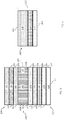
FIG. 1 schematically depicts a photovoltaic device according to one or more embodiments shown and described herein; -
FIG. 2 schematically depicts a substrate according to one or more embodiments shown and described herein; -
FIG. 3 schematically depicts a photovoltaic device according to one or more embodiments shown and described herein; and -
FIGS. 4 and5 schematically depict film stacks for forming absorber layers of photovoltaic devices according to one or more embodiments shown and described herein. - Thin film photovoltaic devices can include multiple layers created on a substrate (or superstrate). For example, a photovoltaic device can include a barrier layer, a transparent conductive oxide (TCO) layer, a buffer layer, an absorber layer, and a back contact layer formed in a stack on a substrate. Each layer may in turn include more than one layer or film. For example, absorber layer can be formed from a plurality of semiconductor layers.
- Referring now to
FIG. 1 , an embodiment of aphotovoltaic device 100 is schematically depicted. Thephotovoltaic device 100 can be configured to receive light and transform light into electrical signals, e.g., photons can be absorbed from the light and transformed into electrical signals via the photovoltaic effect. Accordingly, thephotovoltaic device 100 can define anenergy side 102 configured to be exposed to a light source such as, for example, the sun. Thephotovoltaic device 102 can also define anopposing side 104 offset from theenergy side 102. It is noted that the term "light" can refer to various wavelengths of the electromagnetic spectrum such as, but not limited to, wavelengths in the ultraviolet (UV), infrared (IR), and visible portions of the electromagnetic spectrum. Thephotovoltaic device 100 can include a plurality of layers disposed between theenergy side 102 and theopposing side 104. As used herein, the term "layer" can refer to a thickness of material provided upon a surface. Additionally, each layer can cover all or any portion of the surface. - The
photovoltaic device 100 can include asubstrate 110 configured to facilitate the transmission of light into thephotovoltaic device 100. Thesubstrate 110 can be disposed at theenergy side 102 of thephotovoltaic device 100. Referring collectively toFIGS. 1 and 2 , thesubstrate 110 can have afirst surface 112 substantially facing theenergy side 102 of thephotovoltaic device 100 and asecond surface 114 substantially facing theopposing side 104 of thephotovoltaic device 100. One or more layers of material can be disposed between thefirst surface 112 and thesecond surface 114 of thesubstrate 110. - Referring collectively to
FIGS. 1 and 2 , thesubstrate 110 can include atransparent layer 120 having afirst surface 122 substantially facing theenergy side 102 of thephotovoltaic device 100 and asecond surface 124 substantially facing theopposing side 104 of thephotovoltaic device 100. Thetransparent layer 120 can be formed from a substantially transparent material such as, for example, glass. Suitable glass can include soda-lime glass, or any glass with reduced iron content. Thetransparent layer 120 can have any suitable transmittance, including about 250 nm to about 1,300 nm in some embodiments. Thetransparent layer 120 may also have any suitable transmission percentage, including, for example, more than about 50% in one embodiment, more than about 60% in another embodiment, more than about 70% in yet another embodiment, more than about 80% in a further embodiment, or more than about 85% in still a further embodiment. In one embodiment,transparent layer 120 can be formed from a glass with about 90% transmittance. Optionally, thesubstrate 110 can include acoating 126 applied to thefirst surface 122 of thetransparent layer 120. Thecoating 126 can be configured to interact with light or to improve durability of thesubstrate 110 such as, but not limited to, an antireflective coating, an antisoiling coating, or a combination thereof. - Referring again to
FIG. 1 , thephotovoltaic device 100 can include abarrier layer 130 configured to mitigate diffusion of contaminants (e.g. sodium) from thesubstrate 110, which could result in degradation or delamination. Thebarrier layer 130 can have afirst surface 132 substantially facing theenergy side 102 of thephotovoltaic device 100 and asecond surface 134 substantially facing theopposing side 104 of thephotovoltaic device 100. In some embodiments, thebarrier layer 130 can be provided adjacent to thesubstrate 110. For example, thefirst surface 132 of thebarrier layer 130 can be provided upon thesecond surface 114 of thesubstrate 100. - Generally, the
barrier layer 130 can be substantially transparent, thermally stable, with a reduced number of pin holes and having high sodium-blocking capability, and good adhesive properties. Alternatively or additionally, thebarrier layer 130 can be configured to apply color suppression to the light. Thebarrier layer 130 can include one or more layers of suitable material, including, but not limited to, tin oxide, silicon dioxide, aluminum-doped silicon oxide, silicon oxide, silicon nitride, or aluminum oxide. Thebarrier layer 130 can have any suitable thickness bounded by thefirst surface 132 and thesecond surface 134, including, for example, more than about 500 Å in one embodiment, more than about 750 Å in another embodiment, or less than about 1200 Å in a further embodiment. - Referring still to
FIG. 1 , thephotovoltaic device 100 can include a transparent conductive oxide (TCO)layer 140 configured to provide electrical contact to transport charge carriers generated by thephotovoltaic device 100. TheTCO layer 140 can have afirst surface 142 substantially facing theenergy side 102 of thephotovoltaic device 100 and asecond surface 144 substantially facing theopposing side 104 of thephotovoltaic device 100. In some embodiments, theTCO layer 140 can be provided adjacent to thebarrier layer 130. For example, thefirst surface 142 of thebarrier layer 140 can be provided upon thesecond surface 134 of thebarrier layer 130. Generally, theTCO layer 140 can be formed from one or more layers of n-type semiconductor material that is substantially transparent and has a wide band gap. Specifically, the wide band gap can have a larger energy value compared to the energy of the photons of the light, which can mitigate undesired absorption of light. TheTCO layer 140 can include one or more layers of suitable material, including, but not limited to, tin dioxide, doped tin dioxide (e.g., F-SnO2), indium tin oxide, or cadmium stannate. - The
photovoltaic device 100 can include abuffer layer 150 configured to provide an insulating layer between theTCO layer 140 and any semiconductor layers. Thebuffer layer 150 can have afirst surface 152 substantially facing theenergy side 102 of thephotovoltaic device 100 and asecond surface 154 substantially facing theopposing side 104 of thephotovoltaic device 100. In some embodiments, thebuffer layer 150 can be provided adjacent to theTCO layer 140. For example, thefirst surface 152 of thebuffer layer 150 can be provided upon thesecond surface 144 of theTCO layer 140. Thebuffer layer 140 may include material having higher resistivity than the TCO later 140, including, but not limited to, intrinsic tin dioxide, zinc magnesium oxide (e.g., Zn1-xMgxO), silicon dioxide (SnO2), aluminum oxide (Al2O3), aluminum nitride (AlN), zinc tin oxide, zinc oxide, tin silicon oxide, or a combination thereof. Generally, the material of thebuffer layer 150 can be configured to substantially match the band gap of an adjacent semiconductor layer (e.g., an absorber). Thebuffer layer 150 may have any suitable thickness between thefirst surface 152 and thesecond surface 154, including, for example, more than about 100 Å in one embodiment, between about 100 Å and about 800 Å in another embodiment, or between about 150 Å and about 600 Å in a further embodiment. - The
photovoltaic device 100 can include anabsorber layer 160 configured to form a p-n junction within thephotovoltaic device 100. Accordingly, absorbed photons of the light can free electron-hole pairs and generate carrier flow, which can yield electrical power. Theabsorber layer 160 can have afirst surface 162 substantially facing theenergy side 102 of thephotovoltaic device 100 and asecond surface 164 substantially facing the opposingside 104 of thephotovoltaic device 100. A thickness of theabsorber layer 160 can be defined between thefirst surface 162 and thesecond surface 164. The thickness of theabsorber layer 160 can be between about 0.5 µm to about 10 µm such as, for example, between about 1 µm to about 7 µm in one embodiment, or between about 2 µm to about 5 µm in another embodiment. Theabsorber layer 160 can further include amidpoint 165 located in the middle of the thickness of theabsorber layer 160, i.e., located at the 50% location between thefirst surface 162 and thesecond surface 164 of theabsorber layer 160. - Referring still to
FIG. 1 , theabsorber layer 160 can be formed from a p-type semiconductor material having an excess of positive charge carriers, i.e., holes. Theabsorber layer 160 can include any suitable p-type semiconductor material, including, for example, semi-conductor materials formed from cadmium, tellurium, selenium, sulfur, or any combination thereof. Specific examples include, but are not limited to, cadmium telluride, ternaries of cadmium, selenium and tellurium (e.g., CdSexTe1-x,), ternaries of cadmium, sulfur, and tellurium (e.g., CdSxTe1-x,), quaternaries of cadmium, selenium, sulfur, and tellurium, or their equivalent. In embodiments where theabsorber layer 160 comprises selenium and cadmium, the atomic percent of the selenium can be greater than about 0 atomic percent and less than about 20 atomic compared to cadmium. It is noted that the atomic percent described herein is representative of the entirety of theabsorber layer 160, the atomic percentage of material at a particular location within theabsorber layer 160 can vary with thickness compared to the overall composition of theabsorber layer 160. In embodiments where theabsorber layer 160 comprises sulfur and cadmium, the atomic percent of the sulfur can be greater than about 0 atomic percent and less than about 20 atomic compared to cadmium. It is noted that the concentration of tellurium can vary through the thickness of theabsorber layer 160. For example, when theabsorber layer 160 comprises a ternary of cadmium, selenium, and tellurium (CdSexTe1-x), x can vary in theabsorber layer 160 with distance from thefirst surface 162 of theabsorber layer 160. Similarly, when theabsorber layer 160 comprises a ternary of cadmium, sulfur, and tellurium (CdSxTe1-x), x can vary in theabsorber layer 160 with distance from thefirst surface 162 of theabsorber layer 160. - According to the embodiments provided herein, the
absorber layer 160 can be doped with a dopant configured to manipulate the charge carrier concentration. In some embodiments, the absorber layer can be doped with a group V dopant such as, for example, arsenic, phosphorous, antimony, or a combination thereof. The total dosage of the group V dopant within theabsorber layer 160 can be controlled. In some embodiments, the total dosage of the group V dopant in theabsorber layer 160 is greater than about 0 atomic % and less than about atomic 0.1 %, such as, for example, greater than about 0.001 atomic % and less than about 0.05 atomic % in one embodiment. Alternatively or additionally, the percent concentration profile of the group V dopant through the thickness of theabsorber layer 160. Specifically, the amount of the group V dopant can vary with distance from thefirst surface 162 of theabsorber layer 160. Furthermore, the concentration of oxygen in theabsorber layer 160 can be controlled. Specifically, an average concentration of oxygen in theabsorber layer 160, measured between thefirst surface 162 of theabsorber layer 160 and themidpoint 165 of theabsorber layer 160, can be less or equal to about 3x1017cm-3 such as, for example, less than or equal to about 2x1017cm-3 in one embodiment, between about 5x1015cm-3 and about 3x1017cm-3 in another embodiment, or between about 5x1015cm-3 and about 2x1017cm-3 in a further embodiment. It is noted that the average concentration of oxygen was determined using Time-of-Flight Secondary Ion Mass Spectrometry (TOF-SIMS). - In some embodiments, the
absorber layer 160 can include absorberbuffer interface region 166 formed adjacent to thefirst surface 162 of theabsorber layer 160, and abulk portion 168 from adjacent to the absorberbuffer interface region 166, i.e., between the absorberbuffer interface region 166 and thesecond surface 164 of theabsorber layer 160. For example, the absorberbuffer interface region 166 can span the first 10% of the thickness of theabsorber layer 160 from thefirst surface 162 and thebulk portion 168 can span the remainder of the thickness of theabsorber layer 160. In embodiments where the group V dopant comprises arsenic, the percent concentration profile of arsenic in the absorberbuffer interface region 166 can differ from the percent concentration profile of arsenic in thebulk portion 168. - Referring still to
FIG. 1 , the p-n junction can be formed by providing theabsorber layer 160 sufficiently close to a portion of thephotovoltaic device 100 having an excess of negative charge carriers, i.e., electrons. In some embodiments, theabsorber layer 160 can be provided adjacent to n-type semiconductor material. Alternatively, one or more intervening layers can be provided between theabsorber layer 160 and n-type semiconductor material. In some embodiments, theabsorber layer 160 can be provided adjacent to thebuffer layer 150. For example, thefirst surface 162 of theabsorber layer 160 can be provided upon thesecond surface 154 of thebuffer layer 150. - Referring now to
FIG. 3 , in some embodiments, aphotovoltaic device 200 can include awindow layer 170 comprising n-type semiconductor material. Theabsorber layer 160 can be formed adjacent to thewindow layer 170. Thewindow layer 170 can have afirst surface 172 substantially facing theenergy side 102 of thephotovoltaic device 100 and asecond surface 174 substantially facing the opposingside 104 of thephotovoltaic device 100. In some embodiments, thewindow layer 170 can be positioned between theabsorber layer 160 and theTCO layer 140. In one embodiment, thewindow layer 170 can be positioned between theabsorber layer 160 and thebuffer layer 140. Thewindow layer 170 can include any suitable material, including, for example, cadmium sulfide, zinc sulfide, cadmium zinc sulfide, zinc magnesium oxide, or any combination thereof. - Referring collectively to
FIGS. 1 and3 , thephotovoltaic device 100 can include aback contact layer 180 configured to mitigate undesired alteration of the group V dopant and to provide electrical contact to theabsorber layer 160. Theback contact layer 180 can have afirst surface 182 substantially facing theenergy side 102 of thephotovoltaic device 100 and asecond surface 184 substantially facing the opposingside 104 of thephotovoltaic device 100. A thickness of theback contact layer 180 can be defined between thefirst surface 182 and thesecond surface 184. The thickness of theback contact layer 180 can be between about 5 nm to about 200 nm such as, for example, between about 10 nm to about 50 nm in one embodiment. - In some embodiments, the
back contact layer 180 can be provided adjacent to theabsorber layer 160. For example, thefirst surface 182 of theback contact layer 180 can be provided upon thesecond surface 164 of theabsorber layer 160. In some embodiments, theback contact layer 180 can be substantially copper free, i.e., can be formed from materials that do not include copper. Without being bound to theory, it is believed that copper can interfere with group V dopants (e.g., arsenic). Specifically, theback contact layer 180 can include any suitable material such as, for example, nitrogen-doped zinc telluride (ZnTe), or the like. - The
photovoltaic device 100 can include aconducting layer 190 configured to provide electrical contact with theabsorber layer 160. Theback conducting layer 190 can have afirst surface 192 substantially facing theenergy side 102 of thephotovoltaic device 100 and asecond surface 194 substantially facing the opposingside 104 of thephotovoltaic device 100. In some embodiments, theconducting layer 190 can be provided adjacent to theback contact layer 180. For example, thefirst surface 192 of theconducting layer 190 can be provided upon thesecond surface 184 of theback contact layer 180. Theconducting layer 190 can include any suitable conducting material such as, for example, molybdenum nitride (MoNx) doped with aluminum, molybdenum, or the like. - The
photovoltaic device 100 can include aback support 196 configured to cooperate with thesubstrate 110 to form a housing for thephotovoltaic device 100. Theback support 196 can be disposed at the opposingside 102 of thephotovoltaic device 100. For example, theback support 196 can be formed adjacent to conductinglayer 190. Theback support 196 can include any suitable material, including, for example, glass (e.g., soda-lime glass). - Referring collectively to
FIGS. 4 and5 , theabsorber layer 160 can be formed from a plurality of semiconductor layers 210. For example, the semiconductor layers 210 can be provided as a stack of thin films deposited upon one another using any known deposition technique, including vapor transport deposition. Each of the semiconductor layers 210 can include any suitable p-type semiconductor material, including, for example, semiconductor materials formed from cadmium, tellurium, selenium, sulfur, or any combination thereof. In some embodiments, the material composition of the semiconductor layers 210 can vary. After deposition, the semiconductor layers 210 can be annealed, which can cause the semiconductor layers 210 to diffuse into one another to form a blended material composition having the characteristics described above with respect to theabsorber layer 160. In some embodiments, one or more of the semiconductor layers 210 can be provided as a doped layer, i.e., doped with a group V dopant as described herein. In further embodiments, a majority of theabsorber layer 160 can be formed from the doped layer, i.e., the doped layer can be the thickest of the semiconductor layers 210. - With reference to
FIG. 4 , in some embodiments, the semiconductor layers 210 can comprise afirst semiconductor layer 212, asecond semiconductor layer 214, and athird semiconductor layer 216. Thefirst semiconductor layer 212 can be the layer nearest to thefirst surface 162 of theabsorber layer 160. Thethird semiconductor layer 216 can be the layer nearest to thesecond surface 164 of theabsorber layer 160. Thesecond semiconductor layer 214 can be positioned between thefirst semiconductor layer 212 and thethird semiconductor layer 216. In one embodiment, thefirst semiconductor layer 212 can comprise cadmium selenide (CdSe), thesecond semiconductor layer 214 can comprise cadmium telluride (CdTe), and thethird semiconductor layer 216 can comprise cadmium telluride (CdTe) doped with arsenic. Thethird semiconductor layer 216 can be the thickest layer, and thesecond semiconductor layer 214 can be thicker than thefirst semiconductor layer 212. For example, a ratio of the thickness of thethird semiconductor layer 216 to thefirst semiconductor layer 212 can be greater than about 4 such as, for example, greater than about 6 in one embodiment, or greater than about 8 in another embodiment. A ratio of the thickness of thesecond semiconductor layer 214 to thefirst semiconductor layer 212 can be greater than about 1.1 and less than about 10 such as, for example, greater than about 1.25 and less than about 5 in one embodiment. - In another embodiment, the
first semiconductor layer 212 can comprise cadmium telluride (CdTe), thesecond semiconductor layer 214 can comprise cadmium selenide (CdSe), and thethird semiconductor layer 216 can comprise cadmium telluride (CdTe) doped with arsenic. Thethird semiconductor layer 216 can be the thickest layer, and thesecond semiconductor layer 214 can be thicker than thefirst semiconductor layer 212. - In yet another embodiment, the
first semiconductor layer 212 can comprise a ternary of cadmium, selenium and tellurium (e.g., CdSexTe1-x,), thesecond semiconductor layer 214 can comprise cadmium telluride (CdTe), and thethird semiconductor layer 216 can comprise cadmium telluride (CdTe) doped with arsenic. Thethird semiconductor layer 216 can be the thickest layer, and thefirst semiconductor layer 212 can be thicker than thesecond semiconductor layer 214. - In a further embodiment, the
first semiconductor layer 212 can comprise cadmium sulfide (CdS), thesecond semiconductor layer 214 can comprise cadmium telluride (CdTe), and thethird semiconductor layer 216 can comprise cadmium telluride (CdTe) doped with arsenic. Thethird semiconductor layer 216 can be the thickest layer, and thesecond semiconductor layer 214 can be thicker than thefirst semiconductor layer 212. - Referring still to
FIG. 4 , in some embodiments, thefirst semiconductor layer 212 can comprise cadmium telluride (CdTe), thesecond semiconductor layer 214 can comprise cadmium selenide (CdSe) doped with arsenic, and thethird semiconductor layer 216 can comprise cadmium telluride (CdTe). Alternatively, thethird semiconductor layer 216 can comprise cadmium telluride (CdTe) doped with arsenic. Thethird semiconductor layer 216 can be the thickest layer, and thesecond semiconductor layer 214 can be thicker than thefirst semiconductor layer 212. For example, a ratio of the thickness of thethird semiconductor layer 216 to thefirst semiconductor layer 212 can be greater than about 10 such as, for example, greater than about 20 in one embodiment, or greater than about 25 in another embodiment. A ratio of the thickness of thesecond semiconductor layer 214 to thefirst semiconductor layer 212 can be greater than about 1.1 and less than about 10 such as, for example, greater than about 1.25 and less than about 5 in one embodiment. - According to the embodiments provided herein, the
first semiconductor layer 212 can comprise cadmium telluride (CdTe), thesecond semiconductor layer 214 can comprise cadmium selenide (CdSe), and thethird semiconductor layer 216 can comprise cadmium telluride (CdTe) doped with arsenic. Thethird semiconductor layer 216 can be the thickest layer, and thesecond semiconductor layer 214 can be thicker than thefirst semiconductor layer 212. For example, a ratio of the thickness of thethird semiconductor layer 216 to thefirst semiconductor layer 212 can be greater than about 10, and a ratio of the thickness of thesecond semiconductor layer 214 to thefirst semiconductor layer 212 can be greater than about 1.1 and less than about 10. - With reference to
FIG. 5 , in some embodiments, the semiconductor layers 220 can comprise afirst semiconductor layer 222, and asecond semiconductor layer 224. Thefirst semiconductor layer 222 can be the layer nearest to thefirst surface 162 of theabsorber layer 160. Thesecond semiconductor layer 224 can be the layer nearest to thesecond surface 164 of theabsorber layer 160. In one embodiment, thefirst semiconductor layer 222 can comprise cadmium selenide (CdSe) doped with arsenic, and thesecond semiconductor layer 224 can comprise cadmium telluride (CdTe) doped with arsenic. Thesecond semiconductor layer 224 can be thicker than thefirst semiconductor layer 222. For example, a ratio of the thickness of thesecond semiconductor layer 224 to thefirst semiconductor layer 222 can be greater than about 6 such as, for example, greater than about 8 in one embodiment, or greater than about 10 in another embodiment. - In another embodiment, the
first semiconductor layer 222 can comprise cadmium selenide (CdSe), and thesecond semiconductor layer 224 can comprise cadmium telluride (CdTe) doped with arsenic. Thesecond semiconductor layer 224 can be thicker than thefirst semiconductor layer 222. For example, a ratio of the thickness of thesecond semiconductor layer 224 to thefirst semiconductor layer 222 can be greater than about 7 such as, for example, greater than about 9 in one embodiment, or greater than about 10 in another embodiment. - It should now be understood that the embodiments described herein relate to thin film photovoltaic devices and thin film stacks for use with photovoltaic devices that facilitate the use of group V dopants within p-type semiconductor materials. The described film stacks can provide for operational group V doped p-type CdTe solar devices. Moreover, the back contacts described herein can be provided with copper free material to improve the stability of the dopants.
- According to the embodiments provided herein, a method for forming a photovoltaic device can include depositing a plurality of semiconductor layers. The plurality of semiconductor layers can include a doped layer that is doped with a group V dopant. The doped layer can include cadmium selenide or cadmium telluride. The method can include annealing the plurality of semiconductor layers to form an absorber layer. The absorber layer can include cadmium, selenium, and tellurium. A total dosage of the group V dopant in the absorber layer can be greater than 0 atomic % and less than 0.1 atomic %.
- In a further embodiment, a photovoltaic device can include an absorber layer and a back contact layer. The absorber layer can have a first surface facing an energy side of the photovoltaic device and a second surface facing an opposing side of the photovoltaic device. The absorber layer can include cadmium and tellurium. The absorber layer can be doped with a group V dopant. The back contact layer can be provided upon the second surface of the absorber layer. The back contact layer can include nitrogen-doped zinc telluride.
- In another embodiment, a photovoltaic device can include an absorber layer and a back contact layer. The absorber layer can have a first surface facing an energy side of the photovoltaic device and a second surface facing an opposing side of the photovoltaic device. The absorber layer can include cadmium and tellurium. The absorber layer can be doped with a group V dopant. The back contact layer can be provided upon the second surface of the absorber layer. The back contact layer can be substantially free of copper.
- In yet another embodiment, photovoltaic device can include a buffer layer and an absorber layer. The buffer layer can have a first surface facing an energy side of the photovoltaic device and a second surface facing an opposing side of the photovoltaic device. The absorber layer can be provided upon the second surface of the buffer layer. The absorber layer can be formed from a plurality of semiconductor layers. The plurality of semiconductor layers can include a doped layer comprising cadmium and tellurium. The doped layer can be doped with a group V dopant.
- It is noted that the terms "substantially" and "about" may be utilized herein to represent the inherent degree of uncertainty that may be attributed to any quantitative comparison, value, measurement, or other representation. These terms are also utilized herein to represent the degree by which a quantitative representation may vary from a stated reference without resulting in a change in the basic function of the subject matter at issue.
- While particular embodiments have been illustrated and described herein, it should be understood that various other changes and modifications may be made without departing from the spirit and scope of the claimed subject matter. Moreover, although various aspects of the claimed subject matter have been described herein, such aspects need not be utilized in combination. It is therefore intended that the appended claims cover all such changes and modifications that are within the scope of the claimed subject matter.
- Various preferred features and embodiments of the present invention will now be described with reference to the following numbered paragraphs (paras).
- 1. A method for forming a photovoltaic device comprising:
- depositing a plurality of semiconductor layers, wherein:
- the plurality of semiconductor layers comprise a doped layer that is doped with a group V dopant, and
- the doped layer comprises cadmium selenide, cadmium telluride, or a combination thereof; and
- annealing the plurality of semiconductor layers, whereby an absorber layer is formed, wherein:
- the absorber layer comprises cadmium, selenium, and tellurium, and
- a total dosage of the group V dopant in the absorber layer is greater than 0% and less than 0.1 %.
- depositing a plurality of semiconductor layers, wherein:
- 2. The method of para 1, wherein the doped layer comprises cadmium telluride, and the plurality of semiconductor layers comprises an additional layer comprising cadmium selenide.
- 3. The method of
para 2, wherein the additional layer is doped with arsenic. - 4. The method of
para 2, wherein the doped layer is thicker than the additional layer. - 5. The method of para 4, wherein a ratio of a thickness of the doped layer to a thickness of the additional layer is greater than 6.
- 6. The method of
para 2, wherein the plurality of semiconductor layers comprises a third layer comprising cadmium telluride. - 7. The method of para 6, wherein the additional layer is positioned between the doped layer and the third layer.
- 8. The method of
para 7, wherein the doped layer is a thickest layer, and the additional layer is thicker than the third layer. - 9. The method of para 8, wherein a ratio of a thickness of the doped layer to a thickness of the third layer is greater than 10.
- 10. The method of para 6, wherein the third layer is positioned between the doped layer and the additional layer.
- 11. The method of para 10, wherein the doped layer is a thickest layer, and the doped layer is thicker than the additional layer.
- 12. The method of para 11, wherein a ratio of a thickness of the doped layer to a thickness of the additional layer is greater than 4.
- 13. The method of para 1, comprising forming a back contact layer adj acent to the absorber layer, wherein the back contact is substantially free of copper.
- 14. The method of para 13, wherein:
- the absorber layer has a first surface and a second surface offset by a thickness;
- the back contact is formed upon the second surface of the absorber layer; and
- an average concentration of oxygen in the absorber layer measured between a first surface of the absorber layer and a midpoint of the absorber layer is less than 3x1017cm-3.
- 15. The method of para 13, wherein the back contact layer comprises nitrogen-doped zinc telluride.
- 16. The method of para 15, comprising forming a conducting layer adjacent to the back contact layer.
- 17. The method of para 1, wherein the plurality of semiconductor layers are deposited upon a buffer layer, and the absorber layer has a first surface adjacent to the buffer layer.
- 18. The method of para 17, wherein the doped layer is further from the buffer layer than any other layer of the plurality of semiconductor layers.
- 19. The method of para 18, wherein:
- an absorber buffer interface region is formed adjacent to the first surface of the absorber layer;
- a percent concentration profile of the Group V dopant is formed in the absorber layer with distance from the first surface of the absorber layer; and
- the percent concentration profile of arsenic at the absorber buffer interface differs from the percent concentration profile of arsenic in a bulk portion of the absorber layer.
- 20. The method of para 17, wherein the buffer layer comprises intrinsic tin dioxide, zinc magnesium oxide, silicon dioxide, aluminum oxide, aluminum nitride, or a combination thereof.
- 21. The method of para 1, wherein the group V dopant is arsenic.
- 22. The method of para 1, wherein a majority of the absorber layer is formed from the doped layer.
- 23. The method of para 1, wherein the absorber layer has a thickness between about 0.5 µm to about 10 µm.
- 24. The method of para 1, wherein the group V dopant comprises arsenic, phosphorous, antimony, or a combination thereof.
- 25. The method of para 1, wherein the absorber layer comprises a ternary of cadmium, selenium, and tellurium.
- 26. The method of para 25, wherein the absorber layer comprises greater than about 0 atomic percent and less than about 20 atomic percent of selenium compared to cadmium.
- 27. A photovoltaic device comprising:
- an absorber layer having a first surface facing an energy side of the photovoltaic device and a second surface facing an opposing side of the photovoltaic device, wherein:
- the absorber layer comprises cadmium and tellurium, and
- the absorber layer is doped with a group V dopant, and
- a back contact layer provided upon the second surface of the absorber layer, wherein the back contact layer comprises nitrogen-doped zinc telluride.
- an absorber layer having a first surface facing an energy side of the photovoltaic device and a second surface facing an opposing side of the photovoltaic device, wherein:
- 28. A photovoltaic device comprising:
- an absorber layer having a first surface facing an energy side of the photovoltaic device and a second surface facing an opposing side of the photovoltaic device, wherein:
- the absorber layer comprises cadmium and tellurium, and
- the absorber layer is doped with a group V dopant, and
- a back contact layer provided upon the second surface of the absorber layer, wherein the back contact layer is substantially free of copper.
- an absorber layer having a first surface facing an energy side of the photovoltaic device and a second surface facing an opposing side of the photovoltaic device, wherein:
- 29. The photovoltaic device of any of paras 27-28, comprising a substrate disposed at the energy side of the photovoltaic device.
- 30. The photovoltaic device of any of paras 27-29, comprising a barrier layer provided upon the substrate.
- 31. The photovoltaic device of any of paras 27-30, comprising a transparent conductive oxide layer provided upon the barrier layer.
- 32. The photovoltaic device of any of paras 27-31, comprising a buffer layer provided upon the transparent conductive oxide layer.
- 33. The photovoltaic device of any of paras 27-32, comprising a buffer layer adjacent to the absorber layer.
- 34. The photovoltaic device of para 33, wherein:
- an absorber buffer interface region is formed adjacent to the first surface of the absorber layer;
- the group V dopant comprises arsenic;
- a percent concentration profile of arsenic is formed in the absorber layer with distance from the first surface of the absorber layer; and
- the percent concentration profile of arsenic at the absorber buffer interface differs from the percent concentration profile of arsenic in a bulk portion of the absorber layer.
- 35. The photovoltaic device of para of any of paras 33-34, wherein the buffer layer comprises intrinsic tin dioxide.
- 36. The photovoltaic device of para 33-35, wherein the buffer layer comprises zinc magnesium oxide.
- 37. The photovoltaic device of para 33-36, wherein the buffer layer comprises silicon dioxide.
- 38. The photovoltaic device of para 33-37, wherein the buffer layer comprises aluminum oxide.
- 39. The photovoltaic device of para 33-38, wherein the buffer layer comprises aluminum nitride.
- 40. The photovoltaic device of para 33-39, comprising a conducting layer adjacent to the back contact layer.
- 41. The photovoltaic device of para 40, wherein the conducting layer comprises molybdenum nitride doped with aluminum.
- 42. The photovoltaic device of any of paras 27-41, wherein the back contact layer is substantially free of copper.
- 43. The photovoltaic device of any of paras 27-42, wherein the absorber layer has a thickness between about 0.5 µm to about 10 µm.
- 44. The photovoltaic device of any of paras 27-43, wherein the group V dopant is arsenic.
- 45. The photovoltaic device of any of paras 27-43, wherein the group V dopant is phosphorous.
- 46. The photovoltaic device of any of paras 27-43, wherein the group V dopant is antimony.
- 47. The photovoltaic device of para 44, wherein a total dosage of arsenic in the absorber layer is greater than 0% and less than about 0.1 %.
- 48. The photovoltaic device of any of paras 27-47, wherein the absorber layer comprises selenium.
- 49. The photovoltaic device of any of paras 27-47, wherein the absorber layer comprises sulfur.
- 50. The photovoltaic device of para 48, wherein the absorber layer comprises a ternary of cadmium, selenium, and tellurium.
- 51. The photovoltaic device of para 50, wherein the ternary of cadmium, selenium, and tellurium is given by the formula CdSexTe1-x and x varies in the absorber layer with distance from the first surface of the absorber layer.
- 52. The photovoltaic device of para 50, wherein the ternary of cadmium, selenium, and tellurium is doped with the group V dopant, and wherein the group V dopant comprises arsenic.
- 53. The photovoltaic device of any of paras 27-52, wherein the absorber layer comprises greater than about 0 atomic percent and less than about 20 atomic percent of selenium compared to cadmium.
- 54. The photovoltaic device of any of paras 27-53, wherein the absorber layer comprises greater than about 0 atomic percent and less than about 20 atomic percent of sulfur compared to cadmium.
- 55. A photovoltaic device comprising:
- a buffer layer having a first surface facing an energy side of the photovoltaic device and a second surface facing an opposing side of the photovoltaic device; and
- an absorber layer provided upon the second surface of the buffer layer, wherein:
- the absorber layer is formed from a plurality of semiconductor layers,
- the plurality of semiconductor layers comprises a doped layer comprising cadmium and tellurium, and
- 56. The photovoltaic device of para 55, comprising a substrate disposed at the energy side of the photovoltaic device.
- 57. The photovoltaic device of any of paras 55-56, comprising a barrier layer provided upon the substrate.
- 58. The photovoltaic device of any of paras 55-57, comprising a transparent conductive oxide layer provided upon the barrier layer.
- 59. The photovoltaic device of any of paras 55-58, wherein the buffer layer comprises intrinsic tin dioxide.
- 60. The photovoltaic device of any of paras 55-59, wherein the buffer layer comprises zinc magnesium oxide.
- 61. The photovoltaic device of para 55-60, wherein the second surface of the buffer layer is formed from zinc magnesium oxide.
- 62. The photovoltaic device of any of paras 55-61, wherein the buffer layer comprises silicon dioxide.
- 63. The photovoltaic device of any of paras 55-62, wherein the buffer layer comprises aluminum oxide.
- 64. The photovoltaic device of any of paras 55-63, wherein the buffer layer comprises aluminum nitride.
- 65. The photovoltaic device of any of paras 55-64, wherein the doped layer is further from the second surface of the buffer layer than any other layer of the plurality of semiconductor layers.
- 66. The photovoltaic device of any of paras 55-65, wherein a majority of the absorber layer is formed from the doped layer.
- 67. The photovoltaic device of any of paras 55-66, wherein the plurality of semiconductor layers comprises an additional layer positioned between the second surface of the buffer layer and the doped layer.
- 68. The photovoltaic device of para 67, wherein the additional layer is doped with arsenic.
- 69. The photovoltaic device of any of paras 67-68, wherein the additional layer comprises cadmium and tellurium.
- 70. The photovoltaic device of any of paras 67-68, wherein the additional layer comprises cadmium and selenium.
- 71. The photovoltaic device of any of paras 67-70, wherein the additional layer comprises a ternary of cadmium, selenium, and tellurium.
- 72. The photovoltaic device of any of paras 55-71, wherein the plurality of semiconductor layers comprises a third layer positioned between the second surface of the buffer layer and the additional layer.
- 73. The photovoltaic device of para 72, wherein the third layer comprises cadmium and tellurium.
- 74. The photovoltaic device of para 72, wherein the third layer comprises cadmium and selenium.
- 75. The photovoltaic device of para 72, wherein the third layer comprises a ternary of cadmium, selenium, and tellurium.
- 76. A photovoltaic device comprising:
- a buffer layer having a first surface facing an energy side of the photovoltaic device and a second surface facing an opposing side of the photovoltaic device; and
- an absorber layer provided upon the second surface of the buffer layer, wherein:
- the absorber layer comprises cadmium, selenium, and tellurium, and
- a total dosage of the group V dopant in the absorber layer is greater than 0% and less than 0.1 %
- the absorber layer is formed from a plurality of semiconductor layers,
- the plurality of semiconductor layers comprises a doped layer comprising cadmium selenide or cadmium telluride, and
- the doped layer is doped with a group V dopant.
- 77. The photovoltaic device of para 76, wherein the doped layer comprises cadmium telluride, and the plurality of semiconductor layers comprises an additional layer comprising cadmium selenide
- 78. The photovoltaic device of any of paras 76 or 77, wherein the absorber layer has a first surface nearest an energy side of the photovoltaic device, and wherein an average concentration of oxygen in the absorber layer measured between a first surface of the absorber layer and a midpoint of the absorber layer is less than 3x1017cm-3.
- 79. The method or photovoltaic device of any of
para 2 or paras 77-78, wherein the additional layer is doped with arsenic. - 80. The method or photovoltaic device of any of
para 2 or paras 77-79, wherein the doped layer is thicker than the additional layer. - 81. The method or photovoltaic device of any of
para 2 or paras 77-80, wherein a ratio of a thickness of the doped layer to a thickness of the additional layer is greater than 6. - 82. The method or photovoltaic device of any of
para 2 or paras 77-81, wherein the plurality of semiconductor layers comprises a third layer comprising cadmium telluride. - 83. The method or photovoltaic device of para 82, wherein the additional layer is positioned between the doped layer and the third layer.
- 84. The method or photovoltaic device of para 83, wherein the doped layer is a thickest layer, and the additional layer is thicker than the third layer.
- 85. The method or photovoltaic device of para 84, wherein a ratio of a thickness of the doped layer to a thickness of the third layer is greater than 10.
- 86. The method or photovoltaic device of para 82, wherein the third layer is positioned between the doped layer and the additional layer.
- 87. The method or photovoltaic device of para 86, wherein the doped layer is a thickest layer, and the doped layer is thicker than the additional layer.
- 88. The method or photovoltaic device of para 87, wherein a ratio of a thickness of the doped layer to a thickness of the additional layer is greater than 4.
- 89. The method or photovoltaic device of any of
para 2 or paras 77-88, comprising forming a back contact layer adjacent to the absorber layer, wherein the back contact is substantially free of copper. - 90. The method or photovoltaic device of para 89, wherein the back contact layer comprises nitrogen-doped zinc telluride.
- 91. The method or photovoltaic device of para 90, comprising forming a conducting layer adjacent to the back contact layer.
- 92. The method or photovoltaic device of any of
para 2 or paras 77-91, wherein the plurality of semiconductor layers are deposited upon a buffer layer, and the absorber layer has a first surface adjacent to the buffer layer. - 93. The method or photovoltaic device of para 92, wherein the doped layer is further from the buffer layer than any other layer of the plurality of semiconductor layers.
- 94. The method or photovoltaic device of any of paras 92-93, wherein:
- an absorber buffer interface region is formed adjacent to the first surface of the absorber layer;
- a percent concentration profile of the Group V dopant is formed in the absorber layer with distance from the first surface of the absorber layer; and
- the percent concentration profile of arsenic at the absorber buffer interface differs from the percent concentration profile of arsenic in a bulk portion of the absorber layer.
- 95. The method or photovoltaic device of any of paras 92-94, wherein the buffer layer comprises intrinsic tin dioxide, zinc magnesium oxide, silicon dioxide, aluminum oxide, aluminum nitride, or a combination thereof.
- 96. The method or photovoltaic device of any of
para 2 or paras 77-95, wherein the group V dopant is arsenic. - 97. The method or photovoltaic device of any of
para 2 or paras 77-96, wherein a majority of the absorber layer is formed from the doped layer. - 98. The method or photovoltaic device of any of
para 2 or paras 77-97, wherein the absorber layer has a thickness between about 0.5 µm to about 10 µm. - 99. The method or photovoltaic device of any of
para 2 or paras 77-98, wherein the group V dopant comprises arsenic, phosphorous, antimony, or a combination thereof. - 100. The method or photovoltaic device of any of
para 2 or paras 77-98, wherein the absorber layer comprises a ternary of cadmium, selenium, and tellurium. - 101. The method or photovoltaic device of any of
para 2 or paras 77-100, wherein the absorber layer comprises greater than about 0 atomic percent and less than about 20 atomic percent of selenium compared to cadmium. - 102. The method of any of
para 2 or paras 79-101, wherein an average concentration of oxygen in the absorber layer measured between a first surface of the absorber layer and a midpoint of the absorber layer is less than 3x1017cm-3. - 103. The method of any of
para 2 or paras 79-102, wherein the doped layer comprises a ternary of cadmium, selenium, and tellurium.
Claims (14)
- A photovoltaic device comprising:an absorber layer having a first surface facing an energy side of the photovoltaic device and a second surface facing an opposing side of the photovoltaic device, wherein:the absorber layer comprises cadmium and tellurium, andthe absorber layer is doped with a group V dopant, anda back contact layer provided upon the second surface of the absorber layer, wherein the back contact layer comprises nitrogen-doped zinc telluride or is substantially free of copper.
- The photovoltaic device of claim 1, wherein the group V dopant is arsenic.
- The photovoltaic device of claim 2, wherein a total dosage of arsenic in the absorber layer is greater than 0% and less than about 0.1 %.
- The photovoltaic device of claim 1, wherein the group V dopant is phosphorous.
- The photovoltaic device of claim 1, wherein the group V dopant is antimony.
- The photovoltaic device of any of claims 1-5, comprising a buffer layer adjacent to the absorber layer.
- The photovoltaic device of claim 6, wherein:an absorber buffer interface region is formed adjacent to the first surface of the absorber layer;the group V dopant comprises arsenic;a percent concentration profile of arsenic is formed in the absorber layer with distance from the first surface of the absorber layer; andthe percent concentration profile of arsenic at the absorber buffer interface differs from the percent concentration profile of arsenic in a bulk portion of the absorber layer.
- The photovoltaic device of any of claims 6-7, wherein the buffer layer comprises intrinsic tin dioxide.
- The photovoltaic device of any of claims 6-8, wherein the buffer layer comprises zinc magnesium oxide.
- The photovoltaic device of any of claims 6-9, wherein the buffer layer comprises silicon dioxide.
- The photovoltaic device of any of claims 6-10, wherein the buffer layer comprises aluminum oxide.
- The photovoltaic device of any of claims 6-11, wherein the buffer layer comprises aluminum nitride.
- The photovoltaic device of any of claims 1-12, wherein the absorber layer comprises selenium.
- The photovoltaic device of claim 13, wherein the absorber layer comprises a ternary of cadmium, selenium, and tellurium given by the formula CdSexTe1-x and x varies in the absorber layer with distance from the first surface of the absorber layer.
Applications Claiming Priority (3)
| Application Number | Priority Date | Filing Date | Title |
|---|---|---|---|
| US201762464127P | 2017-02-27 | 2017-02-27 | |
| EP18710271.0A EP3586375B1 (en) | 2017-02-27 | 2018-02-27 | Photovoltaic devices including group v doped thin film stacks |
| PCT/US2018/019848 WO2018157106A1 (en) | 2017-02-27 | 2018-02-27 | Thin film stacks for group v doping, photovoltaic devices including the same, and methods for forming photovoltaic devices with thin film stacks |
Related Parent Applications (2)
| Application Number | Title | Priority Date | Filing Date |
|---|---|---|---|
| EP18710271.0A Division EP3586375B1 (en) | 2017-02-27 | 2018-02-27 | Photovoltaic devices including group v doped thin film stacks |
| EP18710271.0A Division-Into EP3586375B1 (en) | 2017-02-27 | 2018-02-27 | Photovoltaic devices including group v doped thin film stacks |
Publications (2)
| Publication Number | Publication Date |
|---|---|
| EP3719853A1 true EP3719853A1 (en) | 2020-10-07 |
| EP3719853B1 EP3719853B1 (en) | 2025-10-15 |
Family
ID=61617178
Family Applications (2)
| Application Number | Title | Priority Date | Filing Date |
|---|---|---|---|
| EP20174225.1A Active EP3719853B1 (en) | 2017-02-27 | 2018-02-27 | Thin-film photovoltaic devices including cadmium and tellurium doped with group v elements |
| EP18710271.0A Active EP3586375B1 (en) | 2017-02-27 | 2018-02-27 | Photovoltaic devices including group v doped thin film stacks |
Family Applications After (1)
| Application Number | Title | Priority Date | Filing Date |
|---|---|---|---|
| EP18710271.0A Active EP3586375B1 (en) | 2017-02-27 | 2018-02-27 | Photovoltaic devices including group v doped thin film stacks |
Country Status (7)
| Country | Link |
|---|---|
| US (2) | US11342471B2 (en) |
| EP (2) | EP3719853B1 (en) |
| JP (2) | JP6776456B2 (en) |
| CN (2) | CN117038788A (en) |
| AU (1) | AU2018224308B2 (en) |
| MY (1) | MY192457A (en) |
| WO (1) | WO2018157106A1 (en) |
Families Citing this family (18)
| Publication number | Priority date | Publication date | Assignee | Title |
|---|---|---|---|---|
| WO2009058985A1 (en) | 2007-11-02 | 2009-05-07 | First Solar, Inc. | Photovoltaic devices including doped semiconductor films |
| WO2014121187A2 (en) | 2013-02-01 | 2014-08-07 | First Solar, Inc. | Photovoltaic device including a p-n junction and method of manufacturing |
| US11876140B2 (en) | 2013-05-02 | 2024-01-16 | First Solar, Inc. | Photovoltaic devices and method of making |
| US10062800B2 (en) | 2013-06-07 | 2018-08-28 | First Solar, Inc. | Photovoltaic devices and method of making |
| US10529883B2 (en) | 2014-11-03 | 2020-01-07 | First Solar, Inc. | Photovoltaic devices and method of manufacturing |
| AU2018225659B2 (en) | 2017-02-24 | 2023-02-02 | First Solar, Inc. | Doped photovoltaic semiconductor layers and methods of making |
| MY207983A (en) | 2017-12-07 | 2025-03-31 | First Solar Inc | Photovoltaic devices and semiconductor layers with group v dopants and methods for forming the same |
| MY203478A (en) | 2018-02-01 | 2024-06-28 | First Solar Inc | Methods for group v doping of photovoltaic devices |
| CN113261116B (en) * | 2018-10-24 | 2024-10-11 | 第一阳光公司 | Buffer layer for photovoltaic devices with group V doping |
| EP3903352B1 (en) | 2018-12-27 | 2022-03-30 | First Solar, Inc. | Photovoltaic devices and methods of forming the same |
| EP3918637B1 (en) * | 2019-02-06 | 2024-05-22 | First Solar, Inc. | Metal oxynitride back contact layers for photovoltaic devices |
| CN111739959B (en) * | 2020-06-05 | 2021-06-25 | 中国建材国际工程集团有限公司 | A kind of high-efficiency cadmium telluride thin film solar cell and preparation method thereof |
| CN112125286B (en) * | 2020-09-18 | 2022-07-01 | 先导薄膜材料(广东)有限公司 | Arsenic or compound thereof doped cadmium selenide and preparation method thereof, thin film solar cell and preparation method thereof |
| CN112125285B (en) * | 2020-09-18 | 2022-07-01 | 先导薄膜材料(广东)有限公司 | Arsenic-doped or compound-doped cadmium selenide and preparation method thereof, thin-film solar cell and preparation method thereof |
| EP4214761A1 (en) * | 2020-09-21 | 2023-07-26 | First Solar, Inc. | Transparent conducting layers and photovoltaic devices including the same |
| JP2023551904A (en) * | 2020-12-02 | 2023-12-13 | ファースト・ソーラー・インコーポレーテッド | Photovoltaic device and method of fabrication |
| CN114583009B (en) * | 2022-02-18 | 2023-12-29 | 中国建材国际工程集团有限公司 | Cadmium telluride thin film solar cell and preparation method thereof |
| WO2025245020A1 (en) * | 2024-05-20 | 2025-11-27 | First Solar, Inc. | Thin-film back contacts for photovoltaic devices and methods for forming the same |
Citations (3)
| Publication number | Priority date | Publication date | Assignee | Title |
|---|---|---|---|---|
| WO2007129097A2 (en) * | 2006-05-08 | 2007-11-15 | University Of Wales, Bangor | Manufacture of cdte photovoltaic cells using mocvd |
| US20100015753A1 (en) * | 2008-07-17 | 2010-01-21 | James David Garnett | High Power Efficiency, Large Substrate, Polycrystalline CdTe Thin Film Semiconductor Photovoltaic Cell Structures Grown by Molecular Beam Epitaxy at High Deposition Rate for Use in Solar Electricity Generation |
| US20110277812A1 (en) * | 2010-05-13 | 2011-11-17 | Benyamin Buller | Photovoltaic device conducting layer |
Family Cites Families (26)
| Publication number | Priority date | Publication date | Assignee | Title |
|---|---|---|---|---|
| CA1189173A (en) * | 1981-11-20 | 1985-06-18 | Alice W.L. Lin | Elements and methods of preparing elements containing low-resistance contact electrodes for cdte semiconductor materials |
| CN101346823B (en) * | 2005-12-21 | 2010-06-23 | 壳牌可再生能源有限公司 | Method for producing thin-film photovoltaic device and thin-film photovoltaic device |
| WO2009058985A1 (en) | 2007-11-02 | 2009-05-07 | First Solar, Inc. | Photovoltaic devices including doped semiconductor films |
| US9371247B2 (en) * | 2009-05-29 | 2016-06-21 | Corsam Technologies Llc | Fusion formable sodium free glass |
| EP2481094A4 (en) * | 2009-12-10 | 2017-08-09 | Uriel Solar Inc. | HIGH POWER EFFICIENCY POLYCRYSTALLINE CdTe THIN FILM SEMICONDUCTOR PHOTOVOLTAIC CELL STRUCTURES FOR USE IN SOLAR ELECTRICITY GENERATION |
| US8748214B2 (en) * | 2009-12-16 | 2014-06-10 | First Solar, Inc. | Method of p-type doping of cadmium telluride |
| JP2012204477A (en) | 2011-03-24 | 2012-10-22 | Rohm Co Ltd | Light receiving element |
| US9608144B2 (en) * | 2011-06-01 | 2017-03-28 | First Solar, Inc. | Photovoltaic devices and method of making |
| US8990208B2 (en) | 2011-09-22 | 2015-03-24 | Fujitsu Limited | Information management and networking |
| US8822261B2 (en) * | 2011-09-26 | 2014-09-02 | First Solar, Inc. | Methods of making photovoltaic devices |
| JP5860062B2 (en) * | 2011-11-30 | 2016-02-16 | 京セラ株式会社 | Photoelectric conversion device |
| EP2805356A2 (en) | 2012-01-17 | 2014-11-26 | First Solar, Inc | Photovoltaic device having an absorber multilayer and method of manufacturing the same |
| SG11201501197QA (en) * | 2012-08-16 | 2015-04-29 | 3M Innovative Properties Co | Methods of making barrier assemblies |
| WO2014121187A2 (en) * | 2013-02-01 | 2014-08-07 | First Solar, Inc. | Photovoltaic device including a p-n junction and method of manufacturing |
| US9825197B2 (en) * | 2013-03-01 | 2017-11-21 | Taiwan Semiconductor Manufacturing Co., Ltd. | Method of forming a buffer layer in a solar cell, and a solar cell formed by the method |
| US20140261685A1 (en) * | 2013-03-15 | 2014-09-18 | First Solar, Inc. | Thin film photovoltaic device wtih large grain structure and methods of formation |
| WO2014151594A1 (en) * | 2013-03-15 | 2014-09-25 | First Solar, Inc. | High efficiency photovoltaic device employing cadmium sulfide telluride and method of manufacture |
| US10062800B2 (en) | 2013-06-07 | 2018-08-28 | First Solar, Inc. | Photovoltaic devices and method of making |
| US20150171260A1 (en) | 2013-12-17 | 2015-06-18 | Intermolecular Inc. | Low Resistivity Nitrogen-Doped Zinc Telluride and Methods for Forming the Same |
| US20150357502A1 (en) * | 2014-06-05 | 2015-12-10 | EncoreSolar, Inc. | Group iib-via compound solar cells with minimum lattice mismatch and reduced tellurium content |
| US10529883B2 (en) * | 2014-11-03 | 2020-01-07 | First Solar, Inc. | Photovoltaic devices and method of manufacturing |
| WO2016133973A1 (en) * | 2015-02-20 | 2016-08-25 | First Solar, Inc. | A process for making powder alloys containing cadmium and selenium |
| CN106098816A (en) * | 2016-07-13 | 2016-11-09 | 盐城普兰特新能源有限公司 | A kind of cadmium telluride diaphragm solar battery and preparation method thereof |
| AU2018225659B2 (en) | 2017-02-24 | 2023-02-02 | First Solar, Inc. | Doped photovoltaic semiconductor layers and methods of making |
| MY207983A (en) | 2017-12-07 | 2025-03-31 | First Solar Inc | Photovoltaic devices and semiconductor layers with group v dopants and methods for forming the same |
| MY203478A (en) | 2018-02-01 | 2024-06-28 | First Solar Inc | Methods for group v doping of photovoltaic devices |
-
2018
- 2018-02-27 EP EP20174225.1A patent/EP3719853B1/en active Active
- 2018-02-27 US US16/488,808 patent/US11342471B2/en active Active
- 2018-02-27 WO PCT/US2018/019848 patent/WO2018157106A1/en not_active Ceased
- 2018-02-27 JP JP2019546912A patent/JP6776456B2/en active Active
- 2018-02-27 MY MYPI2019004920A patent/MY192457A/en unknown
- 2018-02-27 EP EP18710271.0A patent/EP3586375B1/en active Active
- 2018-02-27 CN CN202311010819.1A patent/CN117038788A/en active Pending
- 2018-02-27 CN CN201880027701.0A patent/CN110546770A/en active Pending
- 2018-02-27 AU AU2018224308A patent/AU2018224308B2/en active Active
-
2020
- 2020-10-07 JP JP2020169527A patent/JP2021007171A/en active Pending
-
2022
- 2022-05-23 US US17/751,189 patent/US12261231B2/en active Active
Patent Citations (3)
| Publication number | Priority date | Publication date | Assignee | Title |
|---|---|---|---|---|
| WO2007129097A2 (en) * | 2006-05-08 | 2007-11-15 | University Of Wales, Bangor | Manufacture of cdte photovoltaic cells using mocvd |
| US20100015753A1 (en) * | 2008-07-17 | 2010-01-21 | James David Garnett | High Power Efficiency, Large Substrate, Polycrystalline CdTe Thin Film Semiconductor Photovoltaic Cell Structures Grown by Molecular Beam Epitaxy at High Deposition Rate for Use in Solar Electricity Generation |
| US20110277812A1 (en) * | 2010-05-13 | 2011-11-17 | Benyamin Buller | Photovoltaic device conducting layer |
Non-Patent Citations (2)
| Title |
|---|
| COLEGROVE ERIC ET AL: "Arsenic doped heteroepitaxial CdTe by MBE for applications in thin-film photovoltaics", 2014 IEEE 40TH PHOTOVOLTAIC SPECIALIST CONFERENCE (PVSC), IEEE, 8 June 2014 (2014-06-08), pages 3261 - 3265, XP032660018, DOI: 10.1109/PVSC.2014.6925632 * |
| JONATHAN D. POPLAWSKY ET AL: "Structural and compositional dependence of the CdTexSe1-x alloy layer photoactivity in CdTe-based solar cells", NATURE COMMUNICATIONS, vol. 7, 27 July 2016 (2016-07-27), pages 12537, XP055473821, DOI: 10.1038/ncomms12537 * |
Also Published As
| Publication number | Publication date |
|---|---|
| WO2018157106A8 (en) | 2019-09-06 |
| JP2020508584A (en) | 2020-03-19 |
| EP3586375A1 (en) | 2020-01-01 |
| WO2018157106A1 (en) | 2018-08-30 |
| EP3719853B1 (en) | 2025-10-15 |
| MY192457A (en) | 2022-08-22 |
| JP2021007171A (en) | 2021-01-21 |
| US20220285569A1 (en) | 2022-09-08 |
| CN110546770A (en) | 2019-12-06 |
| US20200035844A1 (en) | 2020-01-30 |
| AU2018224308A1 (en) | 2019-09-19 |
| CN117038788A (en) | 2023-11-10 |
| JP6776456B2 (en) | 2020-10-28 |
| US11342471B2 (en) | 2022-05-24 |
| US12261231B2 (en) | 2025-03-25 |
| AU2018224308B2 (en) | 2019-11-14 |
| EP3586375B1 (en) | 2020-07-29 |
Similar Documents
| Publication | Publication Date | Title |
|---|---|---|
| US12261231B2 (en) | Thin film stacks for group V doping, photovoltaic devices including the same, and methods for forming photovoltaic devices with thin film stacks | |
| JP6689456B2 (en) | Photovoltaic device with transparent tunnel junction | |
| US11810993B2 (en) | Solar cell, multi-junction solar cell, solar cell module, and photovoltaic power generation system | |
| US20140338741A1 (en) | Conducting substrate for a photovoltaic cell | |
| CN102832262A (en) | Photovoltaic device with reflection enhancing layer | |
| US20240429329A1 (en) | Layer structures for photovoltaic devices and photovoltaic devices including the same | |
| US20250267978A1 (en) | Transparent Conducting Layers and Photovoltaic Devices Including the Same | |
| US20250120219A1 (en) | Buffer Layers for Photovoltaic Devices with Group V Doping | |
| US20240413254A1 (en) | Bifacial enhancement layers and photovoltaic devices including the same | |
| US20140261686A1 (en) | Photovoltaic device with a zinc oxide layer and method of formation | |
| US20200343402A1 (en) | Absorber layers with mercury for photovoltaic devices and methods for forming the same | |
| WO2025057654A1 (en) | Solar cell and manufacturing method for solar cell | |
| WO2020086646A1 (en) | Buffer layers for photovoltaic devices with group v doping | |
| WO2019126463A1 (en) | Absorber layers with mercury for photovoltaic devices and methods for forming the same |
Legal Events
| Date | Code | Title | Description |
|---|---|---|---|
| PUAI | Public reference made under article 153(3) epc to a published international application that has entered the european phase |
Free format text: ORIGINAL CODE: 0009012 |
|
| STAA | Information on the status of an ep patent application or granted ep patent |
Free format text: STATUS: THE APPLICATION HAS BEEN PUBLISHED |
|
| AC | Divisional application: reference to earlier application |
Ref document number: 3586375 Country of ref document: EP Kind code of ref document: P |
|
| AK | Designated contracting states |
Kind code of ref document: A1 Designated state(s): AL AT BE BG CH CY CZ DE DK EE ES FI FR GB GR HR HU IE IS IT LI LT LU LV MC MK MT NL NO PL PT RO RS SE SI SK SM TR |
|
| STAA | Information on the status of an ep patent application or granted ep patent |
Free format text: STATUS: REQUEST FOR EXAMINATION WAS MADE |
|
| 17P | Request for examination filed |
Effective date: 20210407 |
|
| RBV | Designated contracting states (corrected) |
Designated state(s): AL AT BE BG CH CY CZ DE DK EE ES FI FR GB GR HR HU IE IS IT LI LT LU LV MC MK MT NL NO PL PT RO RS SE SI SK SM TR |
|
| RAP3 | Party data changed (applicant data changed or rights of an application transferred) |
Owner name: FIRST SOLAR, INC. |
|
| GRAP | Despatch of communication of intention to grant a patent |
Free format text: ORIGINAL CODE: EPIDOSNIGR1 |
|
| STAA | Information on the status of an ep patent application or granted ep patent |
Free format text: STATUS: GRANT OF PATENT IS INTENDED |
|
| INTG | Intention to grant announced |
Effective date: 20241128 |
|
| GRAJ | Information related to disapproval of communication of intention to grant by the applicant or resumption of examination proceedings by the epo deleted |
Free format text: ORIGINAL CODE: EPIDOSDIGR1 |
|
| STAA | Information on the status of an ep patent application or granted ep patent |
Free format text: STATUS: REQUEST FOR EXAMINATION WAS MADE |
|
| REG | Reference to a national code |
Ref country code: DE Ref legal event code: R079 Free format text: PREVIOUS MAIN CLASS: H01L0031029600 Ipc: H10F0077123000 Ref country code: DE Ref legal event code: R079 Ref document number: 602018086477 Country of ref document: DE Free format text: PREVIOUS MAIN CLASS: H01L0031029600 Ipc: H10F0077123000 |
|
| GRAP | Despatch of communication of intention to grant a patent |
Free format text: ORIGINAL CODE: EPIDOSNIGR1 |
|
| STAA | Information on the status of an ep patent application or granted ep patent |
Free format text: STATUS: GRANT OF PATENT IS INTENDED |
|
| INTC | Intention to grant announced (deleted) | ||
| RIC1 | Information provided on ipc code assigned before grant |
Ipc: H10F 77/123 20250101AFI20250403BHEP |
|
| INTG | Intention to grant announced |
Effective date: 20250506 |
|
| GRAS | Grant fee paid |
Free format text: ORIGINAL CODE: EPIDOSNIGR3 |
|
| GRAA | (expected) grant |
Free format text: ORIGINAL CODE: 0009210 |
|
| STAA | Information on the status of an ep patent application or granted ep patent |
Free format text: STATUS: THE PATENT HAS BEEN GRANTED |
|
| AC | Divisional application: reference to earlier application |
Ref document number: 3586375 Country of ref document: EP Kind code of ref document: P |
|
| AK | Designated contracting states |
Kind code of ref document: B1 Designated state(s): AL AT BE BG CH CY CZ DE DK EE ES FI FR GB GR HR HU IE IS IT LI LT LU LV MC MK MT NL NO PL PT RO RS SE SI SK SM TR |
|
| REG | Reference to a national code |
Ref country code: GB Ref legal event code: FG4D Ref country code: CH Ref legal event code: F10 Free format text: ST27 STATUS EVENT CODE: U-0-0-F10-F00 (AS PROVIDED BY THE NATIONAL OFFICE) Effective date: 20251015 |
|
| REG | Reference to a national code |
Ref country code: IE Ref legal event code: FG4D |
|
| REG | Reference to a national code |
Ref country code: DE Ref legal event code: R096 Ref document number: 602018086477 Country of ref document: DE |
|
| P01 | Opt-out of the competence of the unified patent court (upc) registered |
Free format text: CASE NUMBER: UPC_APP_9246_3719853/2025 Effective date: 20251007 |
|
| REG | Reference to a national code |
Ref country code: NL Ref legal event code: MP Effective date: 20251015 |
|
| REG | Reference to a national code |
Ref country code: AT Ref legal event code: MK05 Ref document number: 1848287 Country of ref document: AT Kind code of ref document: T Effective date: 20251015 |
|
| PG25 | Lapsed in a contracting state [announced via postgrant information from national office to epo] |
Ref country code: NL Free format text: LAPSE BECAUSE OF FAILURE TO SUBMIT A TRANSLATION OF THE DESCRIPTION OR TO PAY THE FEE WITHIN THE PRESCRIBED TIME-LIMIT Effective date: 20251015 |
|
| PG25 | Lapsed in a contracting state [announced via postgrant information from national office to epo] |
Ref country code: ES Free format text: LAPSE BECAUSE OF FAILURE TO SUBMIT A TRANSLATION OF THE DESCRIPTION OR TO PAY THE FEE WITHIN THE PRESCRIBED TIME-LIMIT Effective date: 20251015 |
|
| REG | Reference to a national code |
Ref country code: LT Ref legal event code: MG9D |
|
| PG25 | Lapsed in a contracting state [announced via postgrant information from national office to epo] |
Ref country code: NO Free format text: LAPSE BECAUSE OF FAILURE TO SUBMIT A TRANSLATION OF THE DESCRIPTION OR TO PAY THE FEE WITHIN THE PRESCRIBED TIME-LIMIT Effective date: 20260115 |
|
| PGFP | Annual fee paid to national office [announced via postgrant information from national office to epo] |
Ref country code: DE Payment date: 20260227 Year of fee payment: 9 |
|
| PG25 | Lapsed in a contracting state [announced via postgrant information from national office to epo] |
Ref country code: AT Free format text: LAPSE BECAUSE OF FAILURE TO SUBMIT A TRANSLATION OF THE DESCRIPTION OR TO PAY THE FEE WITHIN THE PRESCRIBED TIME-LIMIT Effective date: 20251015 Ref country code: FI Free format text: LAPSE BECAUSE OF FAILURE TO SUBMIT A TRANSLATION OF THE DESCRIPTION OR TO PAY THE FEE WITHIN THE PRESCRIBED TIME-LIMIT Effective date: 20251015 Ref country code: HR Free format text: LAPSE BECAUSE OF FAILURE TO SUBMIT A TRANSLATION OF THE DESCRIPTION OR TO PAY THE FEE WITHIN THE PRESCRIBED TIME-LIMIT Effective date: 20251015 |
|
| PG25 | Lapsed in a contracting state [announced via postgrant information from national office to epo] |
Ref country code: RS Free format text: LAPSE BECAUSE OF FAILURE TO SUBMIT A TRANSLATION OF THE DESCRIPTION OR TO PAY THE FEE WITHIN THE PRESCRIBED TIME-LIMIT Effective date: 20260115 |
|
| PG25 | Lapsed in a contracting state [announced via postgrant information from national office to epo] |
Ref country code: IS Free format text: LAPSE BECAUSE OF FAILURE TO SUBMIT A TRANSLATION OF THE DESCRIPTION OR TO PAY THE FEE WITHIN THE PRESCRIBED TIME-LIMIT Effective date: 20260215 |
|
| PGFP | Annual fee paid to national office [announced via postgrant information from national office to epo] |
Ref country code: FR Payment date: 20260225 Year of fee payment: 9 |
|
| PG25 | Lapsed in a contracting state [announced via postgrant information from national office to epo] |
Ref country code: PT Free format text: LAPSE BECAUSE OF FAILURE TO SUBMIT A TRANSLATION OF THE DESCRIPTION OR TO PAY THE FEE WITHIN THE PRESCRIBED TIME-LIMIT Effective date: 20260216 |
|
| PG25 | Lapsed in a contracting state [announced via postgrant information from national office to epo] |
Ref country code: PL Free format text: LAPSE BECAUSE OF FAILURE TO SUBMIT A TRANSLATION OF THE DESCRIPTION OR TO PAY THE FEE WITHIN THE PRESCRIBED TIME-LIMIT Effective date: 20251015 |
|
| PG25 | Lapsed in a contracting state [announced via postgrant information from national office to epo] |
Ref country code: LV Free format text: LAPSE BECAUSE OF FAILURE TO SUBMIT A TRANSLATION OF THE DESCRIPTION OR TO PAY THE FEE WITHIN THE PRESCRIBED TIME-LIMIT Effective date: 20251015 |
|
| PG25 | Lapsed in a contracting state [announced via postgrant information from national office to epo] |
Ref country code: BG Free format text: LAPSE BECAUSE OF FAILURE TO SUBMIT A TRANSLATION OF THE DESCRIPTION OR TO PAY THE FEE WITHIN THE PRESCRIBED TIME-LIMIT Effective date: 20251015 |