EP3719834A1 - A method of manufacturing leadframes for semiconductor devices, corresponding leadframe and semiconductor device - Google Patents
A method of manufacturing leadframes for semiconductor devices, corresponding leadframe and semiconductor device Download PDFInfo
- Publication number
- EP3719834A1 EP3719834A1 EP20166392.9A EP20166392A EP3719834A1 EP 3719834 A1 EP3719834 A1 EP 3719834A1 EP 20166392 A EP20166392 A EP 20166392A EP 3719834 A1 EP3719834 A1 EP 3719834A1
- Authority
- EP
- European Patent Office
- Prior art keywords
- electrically
- substrate
- conductive
- pattern
- formations
- Prior art date
- Legal status (The legal status is an assumption and is not a legal conclusion. Google has not performed a legal analysis and makes no representation as to the accuracy of the status listed.)
- Granted
Links
Images



Classifications
-
- H—ELECTRICITY
- H10—SEMICONDUCTOR DEVICES; ELECTRIC SOLID-STATE DEVICES NOT OTHERWISE PROVIDED FOR
- H10W—GENERIC PACKAGES, INTERCONNECTIONS, CONNECTORS OR OTHER CONSTRUCTIONAL DETAILS OF DEVICES COVERED BY CLASS H10
- H10W70/00—Package substrates; Interposers; Redistribution layers [RDL]
- H10W70/01—Manufacture or treatment
- H10W70/04—Manufacture or treatment of leadframes
- H10W70/042—Etching
-
- H—ELECTRICITY
- H10—SEMICONDUCTOR DEVICES; ELECTRIC SOLID-STATE DEVICES NOT OTHERWISE PROVIDED FOR
- H10W—GENERIC PACKAGES, INTERCONNECTIONS, CONNECTORS OR OTHER CONSTRUCTIONAL DETAILS OF DEVICES COVERED BY CLASS H10
- H10W70/00—Package substrates; Interposers; Redistribution layers [RDL]
- H10W70/60—Insulating or insulated package substrates; Interposers; Redistribution layers
- H10W70/62—Insulating or insulated package substrates; Interposers; Redistribution layers characterised by their interconnections
- H10W70/63—Vias, e.g. via plugs
- H10W70/635—Through-vias
-
- H—ELECTRICITY
- H10—SEMICONDUCTOR DEVICES; ELECTRIC SOLID-STATE DEVICES NOT OTHERWISE PROVIDED FOR
- H10W—GENERIC PACKAGES, INTERCONNECTIONS, CONNECTORS OR OTHER CONSTRUCTIONAL DETAILS OF DEVICES COVERED BY CLASS H10
- H10W70/00—Package substrates; Interposers; Redistribution layers [RDL]
- H10W70/40—Leadframes
- H10W70/479—Leadframes on or in insulating or insulated package substrates, interposers, or redistribution layers
-
- H—ELECTRICITY
- H10—SEMICONDUCTOR DEVICES; ELECTRIC SOLID-STATE DEVICES NOT OTHERWISE PROVIDED FOR
- H10W—GENERIC PACKAGES, INTERCONNECTIONS, CONNECTORS OR OTHER CONSTRUCTIONAL DETAILS OF DEVICES COVERED BY CLASS H10
- H10W70/00—Package substrates; Interposers; Redistribution layers [RDL]
- H10W70/01—Manufacture or treatment
- H10W70/04—Manufacture or treatment of leadframes
-
- H—ELECTRICITY
- H10—SEMICONDUCTOR DEVICES; ELECTRIC SOLID-STATE DEVICES NOT OTHERWISE PROVIDED FOR
- H10W—GENERIC PACKAGES, INTERCONNECTIONS, CONNECTORS OR OTHER CONSTRUCTIONAL DETAILS OF DEVICES COVERED BY CLASS H10
- H10W70/00—Package substrates; Interposers; Redistribution layers [RDL]
- H10W70/01—Manufacture or treatment
- H10W70/04—Manufacture or treatment of leadframes
- H10W70/047—Attaching leadframes to insulating supports, e.g. for tape automated bonding [TAB]
-
- H—ELECTRICITY
- H10—SEMICONDUCTOR DEVICES; ELECTRIC SOLID-STATE DEVICES NOT OTHERWISE PROVIDED FOR
- H10W—GENERIC PACKAGES, INTERCONNECTIONS, CONNECTORS OR OTHER CONSTRUCTIONAL DETAILS OF DEVICES COVERED BY CLASS H10
- H10W70/00—Package substrates; Interposers; Redistribution layers [RDL]
- H10W70/01—Manufacture or treatment
- H10W70/04—Manufacture or treatment of leadframes
- H10W70/048—Mechanical treatments, e.g. punching, cutting, deforming or cold welding
-
- H—ELECTRICITY
- H10—SEMICONDUCTOR DEVICES; ELECTRIC SOLID-STATE DEVICES NOT OTHERWISE PROVIDED FOR
- H10W—GENERIC PACKAGES, INTERCONNECTIONS, CONNECTORS OR OTHER CONSTRUCTIONAL DETAILS OF DEVICES COVERED BY CLASS H10
- H10W70/00—Package substrates; Interposers; Redistribution layers [RDL]
- H10W70/01—Manufacture or treatment
- H10W70/05—Manufacture or treatment of insulating or insulated package substrates, or of interposers, or of redistribution layers
- H10W70/095—Manufacture or treatment of insulating or insulated package substrates, or of interposers, or of redistribution layers of vias therein
-
- H—ELECTRICITY
- H10—SEMICONDUCTOR DEVICES; ELECTRIC SOLID-STATE DEVICES NOT OTHERWISE PROVIDED FOR
- H10W—GENERIC PACKAGES, INTERCONNECTIONS, CONNECTORS OR OTHER CONSTRUCTIONAL DETAILS OF DEVICES COVERED BY CLASS H10
- H10W70/00—Package substrates; Interposers; Redistribution layers [RDL]
- H10W70/40—Leadframes
- H10W70/421—Shapes or dispositions
-
- H—ELECTRICITY
- H10—SEMICONDUCTOR DEVICES; ELECTRIC SOLID-STATE DEVICES NOT OTHERWISE PROVIDED FOR
- H10W—GENERIC PACKAGES, INTERCONNECTIONS, CONNECTORS OR OTHER CONSTRUCTIONAL DETAILS OF DEVICES COVERED BY CLASS H10
- H10W70/00—Package substrates; Interposers; Redistribution layers [RDL]
- H10W70/01—Manufacture or treatment
- H10W70/05—Manufacture or treatment of insulating or insulated package substrates, or of interposers, or of redistribution layers
- H10W70/093—Connecting or disconnecting other interconnections thereto or therefrom, e.g. connecting bond wires or bumps
-
- H—ELECTRICITY
- H10—SEMICONDUCTOR DEVICES; ELECTRIC SOLID-STATE DEVICES NOT OTHERWISE PROVIDED FOR
- H10W—GENERIC PACKAGES, INTERCONNECTIONS, CONNECTORS OR OTHER CONSTRUCTIONAL DETAILS OF DEVICES COVERED BY CLASS H10
- H10W70/00—Package substrates; Interposers; Redistribution layers [RDL]
- H10W70/60—Insulating or insulated package substrates; Interposers; Redistribution layers
- H10W70/62—Insulating or insulated package substrates; Interposers; Redistribution layers characterised by their interconnections
- H10W70/65—Shapes or dispositions of interconnections
Definitions
- the description relates to manufacturing semiconductor devices.
- One or more embodiments may be applied to manufacturing leadframes for semiconductor devices such as integrated circuits (ICs), for instance.
- ICs integrated circuits
- So-called "coreless" leadframe technology facilitates using a leadframe as it is, that is without tape apport.
- MIS Molded Interconnect Solutions
- MIS is a leadframe manufacturing technology similar to BGA laminate technology using a molding compound as the core.
- Such a technology facilitates achieving fine inner lead tip pitch (50/60 micron, for instance) which is highly desirable for flip-chip applications.
- An object of one or more embodiments is to overcome the drawbacks discussed in the foregoing.
- One or more embodiments may relate to a corresponding leadframe.
- One or more embodiments may relate to a corresponding device (an integrated circuit, for instance).
- One or more embodiments may use laser direct structuring (LDS) technology in order to create vias and lines with the capability of replacing a metallic frame by metallization of vias and lines.
- LDS laser direct structuring
- references to "an embodiment” or “one embodiment” in the framework of the present description is intended to indicate that a particular configuration, structure, or characteristic described in relation to the embodiment is comprised in at least one embodiment.
- phrases such as “in an embodiment” or “in one embodiment” that may be present in one or more points of the present description do not necessarily refer to one and the same embodiment.
- particular conformations, structures, or characteristics may be combined in any adequate way in one or more embodiments.
- leadframe (or “lead frame”) is currently used (see for instance the USPC Consolidated Glossary of the United States Patent and Trademark Office) to indicate a metal frame which provides support for an integrated circuit chip or die as well as electrical leads to interconnect the integrated circuit in the die or chip to other electrical components or contacts.
- LDS Laser Direct Structuring
- molded parts can be produced with commercially available resins which include additives suitable for the LDS process; a broad range of resins such as polymer resins like PC, PC/ABS, ABS, LCP are currently available for that purpose.
- a laser beam can be used to transfer a desired electrically-conductive pattern on the plastic molding, which is then subjected to metallization (for instance via electroless plating with copper or other metals) to finalize the desired conductive pattern.
- LDS facilitates providing electrically-conductive formations such as vias and lines in a molding compound, without further manufacturing steps and with a high flexibility in the shapes which can be obtained.
- One or more embodiments can be applied to various types of semiconductor devices such as (by way of nonlimiting examples) those semiconductor devices currently referred to as a QFN or QFN-mr, these being acronyms for Quad Flat Pack No-lead and Multirow Quad Flat Pack No-lead.
- Such devices may include leadframes with so-called routed leads, namely electrically-conductive formations (leads) which from an outline location extend inwardly in the direction of a semiconductor chip or die.
- routed leads namely electrically-conductive formations (leads) which from an outline location extend inwardly in the direction of a semiconductor chip or die.
- One or more embodiments may facilitate achieving a reduced (fine) lead tip pitch at the inner (proximal) ends of the leads, that is the ends of the leads towards the semiconductor chip.
- Figures 1A to 1G are exemplary of possible acts in embodiments which may facilitate producing a leadframe (for instance for any one of the various types of semiconductor devices discussed in the foregoing) using LDS technology.
- Figure 1A is exemplary of forming (in a manner known per se to those of skill in the art) a substrate or layer 10 (a laminate core, for instance) of LDS material.
- LDS material such as, for instance, a polymer resin like PC, PC/ABS, ABS, LCP including additives suitable for the LDS process
- PC polymer resin
- PC/ABS polymer resin
- ABS polymer resin
- LCP additives suitable for the LDS process
- Figure 1B is exemplary of an act of structuring the substrate 10 of Figure 1A at the "bottom” or “back” surface thereof, designated 10a.
- Such structuring may involve forming by LDS processing (that is, laser beam machining as schematically indicated at L) a first pattern of electrically-conductive formations 12, 120.
- LDS processing that is, laser beam machining as schematically indicated at L
- Figure 1C is exemplary of an act of structuring the substrate 10 of Figures 1A and 1B at the "top” or “front” surface thereof, designated 10b.
- Such structuring may involve forming, again by LDS processing (that is, laser beam machining L), a second pattern of electrically-conductive formations 14, 140.
- both the first pattern and the second pattern of electrically-conductive formations 12, 120 and 14, 140 can be provided according to any of a virtually boundless variety of possible patterns as desired, by also taking advantage of the intrinsic flexibility LDS laser beam processing.
- Figures 2 and 3 are exemplary of the possibility of performing the acts of Figure 1A to 1F on strip-like material, virtually of indefinite length, to provide (simultaneously) a plurality of lead frames with longitudinal electrically-conductive formations 120, 140 extending along the sides of the strip-like material.
- Figure 1D is exemplary of laser processing (drilling by laser beam L) the substrate 10 having the front and back surfaces 10a, 10b structured as discussed previously to open vias 16 extending at desired locations between the electrically-conductive formations of the two patterns 12, 14 over the two surfaces 10a, 10b.
- Figure 1E is exemplary of similar processing (e.g. laser drilling) possibly applied to the structure of Figure 1D in those embodiments where, as exemplified in Figures 2 and 3 , the acts of Figures 1A to 1G are performed on strip-like material, to provide indexing holes 18 (essentially openings at a given pitch) in the longitudinal electrically-conductive formations 120, 140 or "rails" extending along the sides of the strip-like material.
- processing e.g. laser drilling
- Figure 1F is exemplary of the possibility of growing conductive material (metal such as copper - Cu, for instance) onto the structured paths provided via laser processing of the LDS material as exemplified in Figures 1B to 1E .
- conductive material metal such as copper - Cu, for instance
- Electroless/electrolytic growth as exemplified by EE in Figure 1F may be used for that purpose, that is in order to improve (via growth of copper, for instance) the conductivity of the traces/holes formed in the LDS material by laser processing.
- Electroless processing may facilitate a thicker metal growth.
- electroless alone that is without electrolytic plating
- the conductive formations (traces, for instance) formed with laser processing of LDS material may have a thickness, and thus a conductivity, insufficient for certain applications, such as power devices, for instance: indeed few microns of LDS material may be ablated in the laser activation process (and possibly more in the case of drilling), with the treated material possibly having activated particles (chromium, for instance) at its surface.
- the laser-treated surface portions of the LDS material may not be in relief, but rather recessed.
- Figure 1G is exemplary of an (optional) plating act PT which may be applied with otherwise conventional means in order to provide plated conductive formations over the leads at the bottom side 10a and/or over the lead tips at the top side 10b: see, for instance 12' (material complying with surface mount soldering, for instance) and 1400 (these may be pads or bumps for wire/ribbon bonding or the like) in Figure 1G .
- Figures from 1A to 1G are thus exemplary of a possible manufacturing sequence of an exemplary leadframe including acts of: strip molding ( Figure 1A ), bottom laser structuring ( Figure 1B ), top laser structuring ( Figure 1C ), vias generation connecting the two top/bottom layers ( Figure 1D ), opening of indexing holes (or any other feature as desired) on top/bottom rails ( Figure IE), forming conductive material onto the traces, holes, and so on obtained by laser structuring ( Figure IF), top/bottom layer metallization ( Figure 1G ) .
- all traces, holes obtained by laser structuring may be electroless plated - for less than 10 micron thickness, for instance - or electroplated - up to 50 microns thickness - in case of high current devices, for instance.
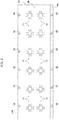
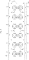
- Figures 2 and 3 are exemplary of a possible result of acts as exemplified in Figures 1A to 1G in a plan view from the top or front side 10b ( Figure 2 ) and from the bottom or back surface 10a ( Figure 3 ).
- Figures 2 and 3 are exemplary of the possibility of performing the acts of Figure 1A to 1F on strip-like material, virtually of indefinite length, to provide a plurality of lead frames to be finally "singulated" (before or after die attachment).
- Such an an act of singulation may be facilitated by using the indexing holes 18 in the longitudinal electrically-conductive formations 120, 140 or "rails".
- leadframe rails 120, 140 may contain features (such as holes 18) which facilitate leadframe indexing and/or unit location into assembly equipment. They can also contain identification codes (2D Codes) and "fiducials" (such as crosses, L shapes, .7) which facilitates properly locating the path of the sawing blade during package singulation.
- identification codes 2D Codes
- fiducials such as crosses, L shapes, .
- Figures 4A and 4B are exemplary of the possibility of applying processing as discussed in connection with the previous figures both to "mono-thickness” substrates 10 and to “dual-thickness” or “multiple-thickness” substrates, for instance having a mesa-like cross sectional profile with a central portion upstanding in comparison with the longitudinal sides of the strip-like structure exemplified in Figures 2 and 3 .
- One or more embodiments as exemplified herein may thus apply to device structure based on a copper dual layer or multiple layer.
- Figure 5 is exemplary of a leadframe adapted to be produced as exemplified herein.
- a single leadframe is exemplified for simplicity showing the presence of a (central) die-mounting area at the top or front surface 10b where a semiconductor die or chip can be attached (by any technique known for that purpose to those of skill in the art as discussed by way of example in the introductory portion of the description) as indicated in dashed lines at C.
- the pattern of electrically-conductive formations 14 may provide an array of routing leads suited to provide electrical coupling of the semiconductor die or chip with contact pads accessible from outside a device package.
- a possible outline of such a package (which may be provided by any technique known for that purpose to those of skill in the art, for instance by molding an epoxy molding compound) is indicated by P in Figure 5 .
- Electrical coupling of the semiconductor die or chip may be via conventional techniques such as wire bonding, stud bumps or the like.
- Figure 5 also exemplifies the possible presence of contact lands or bumps as indicated by 1400' which do not come down to any electrically-conductive formations 14 at the top or front surface 10b but rather correspond to vias 16 formed through the substrate 10 coming down to electrically-conductive formations 12 at the bottom or back surface 10a.
- One or more embodiments as exemplified herein thus adopt laser direct structuring (LDS) processing in order to create electrically-conductive formations such as vias and lines of various types with metallization of vias and lines adapted to replace a metallic frame.
- LDS laser direct structuring
- Figure 5 is exemplary of a "real-world” example providing a leadframe including an array of leads extending between a die-mounting region for mounting a semiconductor chip or die C and the periphery of a substrate 10 of an LDS material.
- leads may have a generally flared shape with a narrow "proximal” tip facing the die mounting area C and a width (and thus area/cross-sectional area) gradually increasing in a "distal" direction away from the die mounting area towards for periphery of the substrate 10.
- final singulation of a lead frame may take place with the die or chip C already attached thereon, possibly with die or chip already electrically coupled and packaged as discussed previously.
- One or more embodiments facilitate providing a device structure with or without plated conductive formations (die pads, for instance) on both sides of the leadframe.
- One or more embodiments may adopt LDS structuring in order to create electrically-conductive formations such as vias and lines with metallization of vias and lines adapted to replace a metallic frame such as conventional leadframes.
- a method of manufacturing leadframes for semiconductor devices as exemplified herein may comprise:
- a method as exemplified herein may comprise applying laser beam processing to said substrate to provide electrically-conductive vias coupled to at least one of the electrically-conductive formations in said first pattern of electrically-conductive formations and at least one of the electrically-conductive formations in said second pattern of electrically-conductive formations (see, for instance 16 in Figures 1D to 1G ).
- a method as exemplified herein may comprise forming (see EE in Figure 1F , for instance) electrically-conductive material onto said first pattern of electrically-conductive formations, said second pattern of electrically-conductive formations and said electrically-conductive vias provided by applying laser beam processing to said substrate.
- said forming electrically-conductive material may comprise electroless and/or electrolytic growth (for instance, electroless plus electrolytic) of electrically-conductive material, such as metal like copper.
- a method as exemplified herein may comprise forming plated contact formations (see, for instance P; 12', 1400 in Figure 1G ) over said first pattern of electrically-conductive formations and/or said second pattern of electrically-conductive formations (optionally, as exemplified in Figure 1G , this may occur "on top" of, that is onto, the electrically-conductive material formed as exemplified in Figure 1F ).
- a method as exemplified herein may comprise:
- a method as exemplified herein may comprise providing, optionally by laser beam drilling of said strip-like laminar substrate, indexing apertures (for instance, 18) sidewise of said strip-like laminar substrate, said indexing apertures providing reference markers in applying singulation to said strip-like laminar substrate.
- a leadframe for semiconductor devices as exemplified herein may comprise:
- a leadframe for semiconductor devices as exemplified herein may comprise electrically-conductive material, optionally metal such as copper, formed onto said portions of said substrate subjected to laser beam processing.
- a leadframe for semiconductor devices as exemplified herein may comprise plated contact formations over said first pattern of electrically-conductive formations and/or said second pattern of electrically-conductive formations (optionally, as exemplified in Figure 1G , these plated contact formations may be provided "on top" of, that is onto, the electrically-conductive material formed onto the portions of the substrate subjected to laser beam processing as exemplified in Figure IF).
- At least one of said first and second pattern of electrically-conductive formations may comprise an array of electrically-conductive formations between a die-mounting area (for instance, C) of said substrate and the periphery of said substrate.
- said array of electrically-conductive formations may comprise electrically-conductive formations having an increasing width away from said die-mounting area and towards the periphery of said substrate.
- a semiconductor device as exemplified herein may comprise:
Landscapes
- Lead Frames For Integrated Circuits (AREA)
- Crystals, And After-Treatments Of Crystals (AREA)
- Wire Bonding (AREA)
Abstract
- providing a laminar substrate (10) of laser direct structuring material, the laminar substrate comprising first (10a) and second (10b) opposed surfaces,
- applying laser beam processing (L) to the substrate (10) to provide a first pattern of electrically-conductive formations (12, 120) at the first surface (10a), a second pattern of electrically-conductive formations (14, 140) at the second surface (10b) and electrically-conductive vias (16) through the substrate (10) between the first surface (10a) and the second surface (10b).



Description
- The description relates to manufacturing semiconductor devices.
- One or more embodiments may be applied to manufacturing leadframes for semiconductor devices such as integrated circuits (ICs), for instance.
- Various technologies are currently available for manufacturing leadframes/substrates for various types of semiconductor devices such as QFN (Quad Flat No-lead), LGA (Land Grid Array), BGA (Ball Grid Array) semiconductor devices.
- So-called "coreless" leadframe technology facilitates using a leadframe as it is, that is without tape apport.
- Solutions currently referred to as MIS (Molded Interconnect Solutions) are exemplary of devices to which coreless leadframe technology may apply.
- Essentially, MIS is a leadframe manufacturing technology similar to BGA laminate technology using a molding compound as the core.
- Such a technology facilitates achieving fine inner lead tip pitch (50/60 micron, for instance) which is highly desirable for flip-chip applications.
- It is noted that such arrangements may exhibit relatively low yield at manufacturing with costs of about 50-100% in excess of "standard" taped leadframes.
- Additionally, certain conventional solutions may exhibit drawbacks related, for instance, to possible warpage (in the case of a metal carrier and a film mold, for instance).
- In the case of MIS technology, notable leadframe warpage may be observed after assembly steps involving a thermal budget such as, for instance:
- die attachment with Die Attach Film (DAF): 100° C, few seconds,
- die attachment with glue/DAF curing 190° C, 1.5 hours,
- wire bonding (WB): 180-220° C, from few seconds to several minutes,
- (package) molding: 175° C, from 40 to 200 seconds,
- Post Mold Curing: 175° C, from 4 to 12 hours.
- An object of one or more embodiments is to overcome the drawbacks discussed in the foregoing.
- According to one or more embodiments, such drawbacks can be overcome by resorting to a method having the features set forth in the claims that follow.
- One or more embodiments may relate to a corresponding leadframe.
- One or more embodiments may relate to a corresponding device (an integrated circuit, for instance).
- The claims are an integral part of the technical disclosure of embodiments as provided herein.
- One or more embodiments may offer one or more of the following advantages:
- simplified processing, which facilites avoiding acts such as metal (copper) lamination, resist lamination, resist exposure, metal etching, resist stripping,
- possible implementation within an IC manufacturing plant (back end),
- reduced cycle time for prototypes,
- reduced cost.
- One or more embodiments may use laser direct structuring (LDS) technology in order to create vias and lines with the capability of replacing a metallic frame by metallization of vias and lines.
- One or more embodiments will now be described, by way of example only, with reference to the annexed figures, wherein:
-
Figures 1A to 1G are exemplary of possible acts in embodiments; -
Figure 2 is a plan view exemplary of embodiments; -
Figure 3 is a plan view exemplary of embodiments from a viewpoint opposite the viewpoint ofFigure 2 ; -
Figures 4A and 4B are exemplary of certain possible features of embodiments; and -
Figure 5 is exemplary of a device which can be produced by resorting to embodiments. - It will be appreciated that, for the sake of clarity and ease of representation, the various figures may not be drawn to a same scale.
- In the ensuing description, one or more specific details are illustrated, aimed at providing an in-depth understanding of examples of embodiments of this description. The embodiments may be obtained without one or more of the specific details, or with other methods, components, materials, etc. In other cases, known structures, materials, or operations are not illustrated or described in detail so that certain aspects of embodiments will not be obscured.
- Reference to "an embodiment" or "one embodiment" in the framework of the present description is intended to indicate that a particular configuration, structure, or characteristic described in relation to the embodiment is comprised in at least one embodiment. Hence, phrases such as "in an embodiment" or "in one embodiment" that may be present in one or more points of the present description do not necessarily refer to one and the same embodiment. Moreover, particular conformations, structures, or characteristics may be combined in any adequate way in one or more embodiments.
- The references used herein are provided merely for convenience and hence do not define the extent of protection or the scope of the embodiments.
- The designation "leadframe" (or "lead frame") is currently used (see for instance the USPC Consolidated Glossary of the United States Patent and Trademark Office) to indicate a metal frame which provides support for an integrated circuit chip or die as well as electrical leads to interconnect the integrated circuit in the die or chip to other electrical components or contacts.
- Laser Direct Structuring (LDS) is a laser-based machining technique now widely used in various sectors of the industrial and consumer electronics markets, for instance for high-performance antenna integration, where an antenna design can be directly formed onto a molded plastic part.
- In an exemplary process, molded parts can be produced with commercially available resins which include additives suitable for the LDS process; a broad range of resins such as polymer resins like PC, PC/ABS, ABS, LCP are currently available for that purpose.
- In LDS, a laser beam can be used to transfer a desired electrically-conductive pattern on the plastic molding, which is then subjected to metallization (for instance via electroless plating with copper or other metals) to finalize the desired conductive pattern.
- One or more embodiments as exemplified herein involve the recognition that LDS facilitates providing electrically-conductive formations such as vias and lines in a molding compound, without further manufacturing steps and with a high flexibility in the shapes which can be obtained.
- One or more embodiments can be applied to various types of semiconductor devices such as (by way of nonlimiting examples) those semiconductor devices currently referred to as a QFN or QFN-mr, these being acronyms for Quad Flat Pack No-lead and Multirow Quad Flat Pack No-lead.
- Such devices may include leadframes with so-called routed leads, namely electrically-conductive formations (leads) which from an outline location extend inwardly in the direction of a semiconductor chip or die.
- One or more embodiments may facilitate achieving a reduced (fine) lead tip pitch at the inner (proximal) ends of the leads, that is the ends of the leads towards the semiconductor chip.
-
Figures 1A to 1G are exemplary of possible acts in embodiments which may facilitate producing a leadframe (for instance for any one of the various types of semiconductor devices discussed in the foregoing) using LDS technology. -
Figure 1A is exemplary of forming (in a manner known per se to those of skill in the art) a substrate or layer 10 (a laminate core, for instance) of LDS material. - Any known LDS material (such as, for instance, a polymer resin like PC, PC/ABS, ABS, LCP including additives suitable for the LDS process) may be used advantageously in embodiments.
-
Figure 1B is exemplary of an act of structuring thesubstrate 10 ofFigure 1A at the "bottom" or "back" surface thereof, designated 10a. - Such structuring may involve forming by LDS processing (that is, laser beam machining as schematically indicated at L) a first pattern of electrically-
conductive formations -
Figure 1C is exemplary of an act of structuring thesubstrate 10 ofFigures 1A and 1B at the "top" or "front" surface thereof, designated 10b. - Such structuring (possibly, but not necessarily, performed after overturning the substrate 10) may involve forming, again by LDS processing (that is, laser beam machining L), a second pattern of electrically-
conductive formations - Those of skill in the art will appreciate that both the first pattern and the second pattern of electrically-
conductive formations - For instance,
Figures 2 and3 are exemplary of the possibility of performing the acts ofFigure 1A to 1F on strip-like material, virtually of indefinite length, to provide (simultaneously) a plurality of lead frames with longitudinal electrically-conductive formations -
Figure 1D is exemplary of laser processing (drilling by laser beam L) thesubstrate 10 having the front andback surfaces vias 16 extending at desired locations between the electrically-conductive formations of the twopatterns surfaces -
Figure 1E is exemplary of similar processing (e.g. laser drilling) possibly applied to the structure ofFigure 1D in those embodiments where, as exemplified inFigures 2 and3 , the acts ofFigures 1A to 1G are performed on strip-like material, to provide indexing holes 18 (essentially openings at a given pitch) in the longitudinal electrically-conductive formations -
Figure 1F is exemplary of the possibility of growing conductive material (metal such as copper - Cu, for instance) onto the structured paths provided via laser processing of the LDS material as exemplified inFigures 1B to 1E . - Electroless/electrolytic growth as exemplified by EE in
Figure 1F may be used for that purpose, that is in order to improve (via growth of copper, for instance) the conductivity of the traces/holes formed in the LDS material by laser processing. - Electroless processing (optionally preceding electrolytic processing) may facilitate a thicker metal growth.
- Also, in those embodiments where a high (Cu, for instance) metal growth is not a desired feature, electroless alone (that is without electrolytic plating) can be used.
- It is noted that the conductive formations (traces, for instance) formed with laser processing of LDS material may have a thickness, and thus a conductivity, insufficient for certain applications, such as power devices, for instance: indeed few microns of LDS material may be ablated in the laser activation process (and possibly more in the case of drilling), with the treated material possibly having activated particles (chromium, for instance) at its surface.
- Also, while exemplified in relief in the figures for simplicity and ease of understanding, the laser-treated surface portions of the LDS material may not be in relief, but rather recessed.
- Those of skill in the art will thus appreciate that passing from an "intermediate" structure obtained (solely) via laser activation to a resulting final structure may involve such a step as exemplified in
Figure 1F , that is forming e.g. electroplated conductive formations. -
Figure 1G is exemplary of an (optional) plating act PT which may be applied with otherwise conventional means in order to provide plated conductive formations over the leads at thebottom side 10a and/or over the lead tips at thetop side 10b: see, for instance 12' (material complying with surface mount soldering, for instance) and 1400 (these may be pads or bumps for wire/ribbon bonding or the like) inFigure 1G . - Figures from 1A to 1G are thus exemplary of a possible manufacturing sequence of an exemplary leadframe including acts of: strip molding (
Figure 1A ), bottom laser structuring (Figure 1B ), top laser structuring (Figure 1C ), vias generation connecting the two top/bottom layers (Figure 1D ), opening of indexing holes (or any other feature as desired) on top/bottom rails (Figure IE), forming conductive material onto the traces, holes, and so on obtained by laser structuring (Figure IF), top/bottom layer metallization (Figure 1G ) . - For instance, in an act as exemplified in
Figure 1F , all traces, holes obtained by laser structuring (seeFigures 1B to 1E , for example) may be electroless plated - for less than 10 micron thickness, for instance - or electroplated - up to 50 microns thickness - in case of high current devices, for instance. -
Figures 2 and3 are exemplary of a possible result of acts as exemplified inFigures 1A to 1G in a plan view from the top orfront side 10b (Figure 2 ) and from the bottom or backsurface 10a (Figure 3 ). - As discussed,
Figures 2 and3 are exemplary of the possibility of performing the acts ofFigure 1A to 1F on strip-like material, virtually of indefinite length, to provide a plurality of lead frames to be finally "singulated" (before or after die attachment). - Such an an act of singulation may be facilitated by using the indexing holes 18 in the longitudinal electrically-
conductive formations - Indeed,
such leadframe rails -
Figures 4A and 4B are exemplary of the possibility of applying processing as discussed in connection with the previous figures both to "mono-thickness"substrates 10 and to "dual-thickness" or "multiple-thickness" substrates, for instance having a mesa-like cross sectional profile with a central portion upstanding in comparison with the longitudinal sides of the strip-like structure exemplified inFigures 2 and3 . One or more embodiments as exemplified herein may thus apply to device structure based on a copper dual layer or multiple layer. -
Figure 5 is exemplary of a leadframe adapted to be produced as exemplified herein. - A single leadframe is exemplified for simplicity showing the presence of a (central) die-mounting area at the top or
front surface 10b where a semiconductor die or chip can be attached (by any technique known for that purpose to those of skill in the art as discussed by way of example in the introductory portion of the description) as indicated in dashed lines at C. - As exemplified in
Figure 5 , the pattern of electrically-conductive formations 14 may provide an array of routing leads suited to provide electrical coupling of the semiconductor die or chip with contact pads accessible from outside a device package. A possible outline of such a package (which may be provided by any technique known for that purpose to those of skill in the art, for instance by molding an epoxy molding compound) is indicated by P inFigure 5 . - Electrical coupling of the semiconductor die or chip may be via conventional techniques such as wire bonding, stud bumps or the like.
- Whatever the option(s) adopted for that purpose, such coupling may take advantage of the provision of contact formations as indicated by 1400 in
Figure 5 . -
Figure 5 also exemplifies the possible presence of contact lands or bumps as indicated by 1400' which do not come down to any electrically-conductive formations 14 at the top orfront surface 10b but rather correspond tovias 16 formed through thesubstrate 10 coming down to electrically-conductive formations 12 at the bottom or backsurface 10a. - One or more embodiments as exemplified herein thus adopt laser direct structuring (LDS) processing in order to create electrically-conductive formations such as vias and lines of various types with metallization of vias and lines adapted to replace a metallic frame.
-
Figure 5 is exemplary of a "real-world" example providing a leadframe including an array of leads extending between a die-mounting region for mounting a semiconductor chip or die C and the periphery of asubstrate 10 of an LDS material. As exemplified inFigure 5 , one or more of these leads may have a generally flared shape with a narrow "proximal" tip facing the die mounting area C and a width (and thus area/cross-sectional area) gradually increasing in a "distal" direction away from the die mounting area towards for periphery of thesubstrate 10. - As noted, final singulation of a lead frame (as exemplified by arrows S in
Figure 5 ) may take place with the die or chip C already attached thereon, possibly with die or chip already electrically coupled and packaged as discussed previously. - One or more embodiments facilitate providing a device structure with or without plated conductive formations (die pads, for instance) on both sides of the leadframe.
- One or more embodiments may adopt LDS structuring in order to create electrically-conductive formations such as vias and lines with metallization of vias and lines adapted to replace a metallic frame such as conventional leadframes.
- A method of manufacturing leadframes for semiconductor devices as exemplified herein may comprise:
- providing a laminar substrate (for instance, 10) of laser direct structuring material, the laminar substrate comprising first (for instance, bottom or back
surface 10a) and second (for instance, top orfront surface 10b) opposed surfaces, - applying laser beam processing (for instance, L) to said substrate to provide a first pattern of electrically-conductive formations (for instance, 12, 120) at the first surface of said substrate, a second pattern of electrically-conductive formations (for instance, 14, 140) at the second surface of said substrate, and electrically-conductive vias (for instance, 16) through said substrate between the first surface of said substrate (10) and the second surface of said substrate, the electrically-conductive vias coupled to at least one (that is, to both of 12, 14, see, for
instance Figures 1D to 1G or even just one, see, for instance and 1400' inFigure 5 , where 1400' are coupled only to 12 on the bottom of back side) of the electrically-conductive formations in said first pattern of electrically-conductive formations and said second pattern of electrically-conductive formations. - A method as exemplified herein may comprise applying laser beam processing to said substrate to provide electrically-conductive vias coupled to at least one of the electrically-conductive formations in said first pattern of electrically-conductive formations and at least one of the electrically-conductive formations in said second pattern of electrically-conductive formations (see, for
instance 16 inFigures 1D to 1G ). - A method as exemplified herein may comprise forming (see EE in
Figure 1F , for instance) electrically-conductive material onto said first pattern of electrically-conductive formations, said second pattern of electrically-conductive formations and said electrically-conductive vias provided by applying laser beam processing to said substrate. - In a method as exemplified herein, said forming electrically-conductive material may comprise electroless and/or electrolytic growth (for instance, electroless plus electrolytic) of electrically-conductive material, such as metal like copper.
- A method as exemplified herein may comprise forming plated contact formations (see, for instance P; 12', 1400 in
Figure 1G ) over said first pattern of electrically-conductive formations and/or said second pattern of electrically-conductive formations (optionally, as exemplified inFigure 1G , this may occur "on top" of, that is onto, the electrically-conductive material formed as exemplified inFigure 1F ). - A method as exemplified herein may comprise:
- providing a strip-like laminar substrate (see, for instance,
Figures 2 and3 ) of laser direct structuring material and applying laser beam processing to said strip-like laminar substrate to provide a plurality of assemblies each including a first pattern of electrically-conductive formations at the first surface of said substrate, a second pattern of electrically-conductive formations at the second surface of said substrate, and electrically-conductive vias through said substrate between the first surface of said substrate and the second surface of said substrate, the electrically-conductive vias coupled to at least one (see 12, 14 inFigures 1D to 1F and 1400' inFigure 5 , where 1400' are coupled only to 12 on the bottom of back side) of the electrically-conductive formations in said first pattern of electrically-conductive formations and said second pattern of electrically-conductive formations, - applying singulation (for instance, S in
Figure 5 ) to said strip-like laminar substrate after application of laser beam processing, said singulation to separate the assemblies in said plurality of assemblies. - A method as exemplified herein may comprise providing, optionally by laser beam drilling of said strip-like laminar substrate, indexing apertures (for instance, 18) sidewise of said strip-like laminar substrate, said indexing apertures providing reference markers in applying singulation to said strip-like laminar substrate.
- A leadframe for semiconductor devices as exemplified herein may comprise:
- a laminar substrate of laser direct structuring material, the laminar substrate comprising first and second opposed surfaces, and
- portions (for instance, 12, 120, 14, 140, 16) of said substrate subjected to laser beam processing as exemplified herein.
- A leadframe for semiconductor devices as exemplified herein may comprise electrically-conductive material, optionally metal such as copper, formed onto said portions of said substrate subjected to laser beam processing.
- A leadframe for semiconductor devices as exemplified herein may comprise plated contact formations over said first pattern of electrically-conductive formations and/or said second pattern of electrically-conductive formations (optionally, as exemplified in
Figure 1G , these plated contact formations may be provided "on top" of, that is onto, the electrically-conductive material formed onto the portions of the substrate subjected to laser beam processing as exemplified in Figure IF). - In a leadframe for semiconductor devices as exemplified herein, at least one of said first and second pattern of electrically-conductive formations may comprise an array of electrically-conductive formations between a die-mounting area (for instance, C) of said substrate and the periphery of said substrate.
- In a leadframe for semiconductor devices as exemplified herein, said array of electrically-conductive formations may comprise electrically-conductive formations having an increasing width away from said die-mounting area and towards the periphery of said substrate.
- A semiconductor device as exemplified herein may comprise:
- one (or more) leadframe(s) as exemplified herein,
- one (or more) semiconductor chip(s) or die/dice (for instance, C) attached to said leadframe, the at least one semiconductor chip or die electrically coupled to electrically-conductive formations out of said first pattern of electrically-conductive formations at the first surface of said substrate, said second pattern of electrically-conductive formations at the second surface of said substrate and said electrically-conductive vias .
- Without prejudice to the underlying principles, the details and embodiments may vary, even significantly, with respect to what has been described by way of example only, without departing from the extent of protection.
- The extent of protection is determined by the annexed claims.
Claims (13)
- A method of manufacturing leadframes for semiconductor devices, the method comprising:- providing a laminar substrate (10) of laser direct structuring material, the laminar substrate comprising first (10a) and second (10b) opposed surfaces,- applying laser beam processing (L) to said substrate (10) to provide a first pattern of electrically-conductive formations (12, 120) at the first surface (10a) of said substrate (10), a second pattern of electrically-conductive formations (14, 140) at the second surface (10b) of said substrate (10), and electrically-conductive vias (16) through said substrate (10) between the first surface (10a) of said substrate (10) and the second surface (10b) of said substrate (10), the electrically-conductive vias (16) coupled to at least one (12, 14) of the electrically-conductive formations in said first pattern of electrically-conductive formations and said second pattern of electrically-conductive formations.
- The method of claim 1, comprising applying laser beam processing (L) to said substrate (10) to provide electrically-conductive vias (16) coupled to at least one (12) of the electrically-conductive formations in said first pattern of electrically-conductive formations and at least one (14) of the electrically-conductive formations in said second pattern of electrically-conductive formations.
- The method of claim 1 or claim 2, comprising forming (EE) electrically-conductive material onto said first pattern of electrically-conductive formations (12, 120), said second pattern of electrically-conductive formations (14, 140) and said electrically-conductive vias (16) provided by applying laser beam processing (L) to said substrate (10).
- The method of claim 3, wherein said forming (EE) electrically-conductive material comprises electroless and/or electrolytic growth of electrically-conductive material.
- The method of any of the previous claims, comprising forming plated contact formations (P; 12', 1400) over said first pattern of electrically-conductive formations (12, 120) and/or said second pattern of electrically-conductive formations (14, 140) .
- The method of any of the previous claims, comprising:- providing a strip-like laminar substrate (10) of laser direct structuring material and applying laser beam processing (L) to said strip-like laminar substrate (10) to provide a plurality of assemblies each including a first pattern of electrically-conductive formations (12, 120) at the first surface (10a) of said substrate (10), a second pattern of electrically-conductive formations (14, 140) at the second surface (10b) of said substrate (10), and electrically-conductive vias (16) through said substrate (10) between the first surface (10a) of said substrate (10) and the second surface (10b) of said substrate (10), the electrically-conductive vias (16) coupled to at least one (12, 14) of the electrically-conductive formations in said first pattern of electrically-conductive formations and said second pattern of electrically-conductive formations,- applying singulation (S) to said strip-like laminar substrate (10) after application of laser beam processing (L), said singulation to separate the assemblies in said plurality of assemblies.
- The method of claim 6, comprising providing, preferably by laser beam drilling of said strip-like laminar substrate (10), indexing apertures (18) sidewise of said strip-like laminar substrate (10), said indexing apertures providing reference markers in applying singulation (S) to said strip-like laminar substrate (10).
- A leadframe for semiconductor devices, the leadframe comprising:- a laminar substrate (10) of laser direct structuring material, the laminar substrate comprising first (10a) and second (10b) opposed surfaces, and- portions (12, 120, 14, 140, 16) of said substrate (10) subjected to laser beam processing (L) with the method of any of the previous claims.
- The leadframe of claim 8, comprising electrically-conductive material, preferably a metal such as copper, formed onto said portions (12, 120, 14, 140, 16) of said substrate (10) subjected to laser beam processing (L).
- The leadframe of claim 8 or claim 9, comprising plated contact formations (P; 12', 1400) over said first pattern of electrically-conductive formations (12, 120) and/or said second pattern of electrically-conductive formations (14, 140).
- The leadframe of any of claims 8 to 10, wherein at least one of said first (12) and second (14) pattern of electrically-conductive formations comprises an array of electrically-conductive formations between a die-mounting area (C) of said substrate (10) and the periphery of said substrate (10).
- The leadframe of claim 11, wherein said array of electrically-conductive formations comprises electrically-conductive formations having an increasing width away from said die-mounting area (C) and towards the periphery of said substrate (10).
- A semiconductor device comprising:- at least one leadframe according to any of claims claim 8 to 12,- at least one semiconductor chip or die (C) attached to said leadframe, the at least one semiconductor chip or die (C) electrically coupled to electrically-conductive formations out of said first pattern of electrically-conductive formations (12, 120) at the first surface (10a) of said substrate (10), said second pattern of electrically-conductive formations (14, 140) at the second surface (10b) of said substrate (10) and said electrically-conductive vias (16).
Applications Claiming Priority (1)
| Application Number | Priority Date | Filing Date | Title |
|---|---|---|---|
| IT102019000005156A IT201900005156A1 (en) | 2019-04-05 | 2019-04-05 | PROCEDURE FOR MANUFACTURING LEADFRAME FOR SEMICONDUCTOR DEVICES |
Publications (2)
| Publication Number | Publication Date |
|---|---|
| EP3719834A1 true EP3719834A1 (en) | 2020-10-07 |
| EP3719834B1 EP3719834B1 (en) | 2025-06-04 |
Family
ID=67002293
Family Applications (1)
| Application Number | Title | Priority Date | Filing Date |
|---|---|---|---|
| EP20166392.9A Active EP3719834B1 (en) | 2019-04-05 | 2020-03-27 | A method of manufacturing leadframes for semiconductor devices |
Country Status (4)
| Country | Link |
|---|---|
| US (2) | US11462465B2 (en) |
| EP (1) | EP3719834B1 (en) |
| CN (2) | CN213546266U (en) |
| IT (1) | IT201900005156A1 (en) |
Cited By (3)
| Publication number | Priority date | Publication date | Assignee | Title |
|---|---|---|---|---|
| EP4016614A1 (en) * | 2020-12-17 | 2022-06-22 | STMicroelectronics S.r.l. | Method of manufacturing multi-die semiconductor devices |
| US11887959B2 (en) | 2020-12-17 | 2024-01-30 | Stmicroelectronics S.R.L. | Chip-on-lead semiconductor device, and corresponding method of manufacturing chip-on-lead semiconductor devices |
| US12368055B2 (en) | 2020-12-17 | 2025-07-22 | Stmicroelectronics S.R.L. | Method of manufacturing multi-die semiconductor devices and corresponding multi-die semiconductor device |
Families Citing this family (27)
| Publication number | Priority date | Publication date | Assignee | Title |
|---|---|---|---|---|
| IT201900005156A1 (en) * | 2019-04-05 | 2020-10-05 | St Microelectronics Srl | PROCEDURE FOR MANUFACTURING LEADFRAME FOR SEMICONDUCTOR DEVICES |
| IT201900024292A1 (en) | 2019-12-17 | 2021-06-17 | St Microelectronics Srl | PROCEDURE FOR MANUFACTURING SEMICONDUCTOR DEVICES AND CORRESPONDING SEMICONDUCTOR DEVICE |
| CN112885726B (en) * | 2021-01-19 | 2022-03-25 | 杭州梵特斯科技有限公司 | Intelligent power chip structure and manufacturing method thereof |
| IT202100001301A1 (en) | 2021-01-25 | 2022-07-25 | St Microelectronics Srl | SEMICONDUCTOR DEVICE AND CORRESPONDING MANUFACTURING PROCEDURE |
| IT202100014198A1 (en) | 2021-05-31 | 2022-12-01 | St Microelectronics Srl | Process for manufacturing semiconductor devices and corresponding semiconductor device |
| IT202100014306A1 (en) | 2021-06-01 | 2022-12-01 | St Microelectronics Srl | Process for manufacturing semiconductor devices and corresponding semiconductor device |
| IT202100014906A1 (en) | 2021-06-08 | 2022-12-08 | St Microelectronics Srl | Process for manufacturing semiconductor devices and corresponding semiconductor device |
| IT202100017213A1 (en) | 2021-06-30 | 2022-12-30 | St Microelectronics Srl | Process for manufacturing semiconductor devices and corresponding semiconductor device |
| US12525512B2 (en) | 2021-07-30 | 2026-01-13 | Stmicroelectronics S.R.L. | Method of coupling semiconductor dice and corresponding semiconductor device |
| US12500148B2 (en) | 2021-07-30 | 2025-12-16 | Stmicroelectronics S.R.L. | Method of coupling semiconductor dice, tool for use therein and corresponding semiconductor device |
| IT202100022607A1 (en) | 2021-08-31 | 2023-03-03 | St Microelectronics Srl | Process for manufacturing semiconductor devices and corresponding semiconductor device |
| US12080631B2 (en) | 2021-08-31 | 2024-09-03 | Stmicroelectronics S.R.L. | Leadframe-less laser direct structuring (LDS) package |
| IT202100028553A1 (en) | 2021-11-10 | 2023-05-10 | St Microelectronics Srl | PROCEDURE FOR MANUFACTURING SEMICONDUCTOR DEVICES AND CORRESPONDING SEMICONDUCTOR DEVICE |
| IT202200008897A1 (en) | 2022-05-03 | 2023-11-03 | St Microelectronics Srl | Process for manufacturing semiconductor devices and corresponding semiconductor device |
| IT202200008891A1 (en) | 2022-05-03 | 2023-11-03 | St Microelectronics Srl | Process for manufacturing semiconductor devices and corresponding semiconductor device |
| IT202200011561A1 (en) | 2022-05-31 | 2023-12-01 | St Microelectronics Srl | Process for manufacturing semiconductor devices and corresponding semiconductor device |
| IT202200016011A1 (en) | 2022-07-28 | 2024-01-28 | St Microelectronics Srl | PROCEDURE FOR MANUFACTURING SEMICONDUCTOR DEVICES AND CORRESPONDING SEMICONDUCTOR DEVICE |
| EP4312250A1 (en) | 2022-07-28 | 2024-01-31 | STMicroelectronics S.r.l. | Method of manufacturing semiconductor devices, corresponding substrate and semiconductor device |
| IT202200022416A1 (en) | 2022-11-02 | 2024-05-02 | St Microelectronics Srl | Process for manufacturing semiconductor devices and corresponding semiconductor device |
| IT202200022443A1 (en) | 2022-11-02 | 2024-05-02 | St Microelectronics Srl | Process for fabricating semiconductor devices, leadframe, die and corresponding semiconductor device |
| IT202300006129A1 (en) | 2023-03-29 | 2024-09-29 | St Microelectronics Int Nv | PROCEDURE FOR MANUFACTURING SEMICONDUCTOR DEVICES AND CORRESPONDING SEMICONDUCTOR DEVICE |
| IT202300014250A1 (en) | 2023-07-07 | 2025-01-07 | St Microelectronics Int Nv | PROCEDURE FOR MANUFACTURING SEMICONDUCTOR DEVICES AND CORRESPONDING SEMICONDUCTOR DEVICE |
| IT202300017841A1 (en) | 2023-08-30 | 2025-03-02 | St Microelectronics Int Nv | PROCEDURE FOR MANUFACTURING SEMICONDUCTOR DEVICES AND CORRESPONDING SEMICONDUCTOR DEVICE |
| IT202300020505A1 (en) | 2023-10-04 | 2025-04-04 | St Microelectronics Int Nv | PROCEDURE FOR MANUFACTURING SEMICONDUCTOR DEVICES AND CORRESPONDING DEVICE |
| IT202300024078A1 (en) | 2023-11-14 | 2025-05-14 | St Microelectronics Int Nv | PROCEDURE FOR MANUFACTURING THERMOELECTRIC GENERATORS |
| IT202400004246A1 (en) | 2024-02-28 | 2025-08-28 | St Microelectronics Int Nv | PROCEDURE FOR MANUFACTURING SEMICONDUCTOR DEVICES AND CORRESPONDING DEVICE |
| IT202400004300A1 (en) | 2024-02-28 | 2025-08-28 | St Microelectronics Int Nv | PROCEDURE FOR MANUFACTURING SEMICONDUCTOR DEVICES AND CORRESPONDING SEMICONDUCTOR DEVICE |
Citations (5)
| Publication number | Priority date | Publication date | Assignee | Title |
|---|---|---|---|---|
| EP0227371A1 (en) * | 1985-12-11 | 1987-07-01 | Kabushiki Kaisha Toshiba | Ceramic substrates and methods of manufacturing same |
| US20070144769A1 (en) * | 2005-12-28 | 2007-06-28 | Intel Corporation | Method and apparatus for a printed circuit board using laser assisted metallization and patterning of a substrate |
| US9171739B1 (en) * | 2014-06-24 | 2015-10-27 | Stats Chippac Ltd. | Integrated circuit packaging system with coreless substrate and method of manufacture thereof |
| US20180342453A1 (en) * | 2017-05-23 | 2018-11-29 | Stmicroelectronics S.R.L. | Method of manufacturing semiconductor devices and corresponding product |
| US20190006191A1 (en) * | 2017-06-30 | 2019-01-03 | Stmicroelectronics S.R.L. | Semiconductor product and corresponding method |
Family Cites Families (10)
| Publication number | Priority date | Publication date | Assignee | Title |
|---|---|---|---|---|
| US8323802B2 (en) * | 2004-10-20 | 2012-12-04 | E I Du Pont De Nemours And Company | Light activatable polyimide compositions for receiving selective metalization, and methods and compositions related thereto |
| US8338936B2 (en) * | 2008-07-24 | 2012-12-25 | Infineon Technologies Ag | Semiconductor device and manufacturing method |
| US8686300B2 (en) * | 2008-12-24 | 2014-04-01 | Ibiden Co., Ltd. | Printed wiring board and method for manufacturing the same |
| JP5325736B2 (en) * | 2009-10-06 | 2013-10-23 | 新光電気工業株式会社 | Semiconductor device and manufacturing method thereof |
| US20110095410A1 (en) * | 2009-10-28 | 2011-04-28 | Fairchild Semiconductor Corporation | Wafer level semiconductor device connector |
| TW201225238A (en) * | 2010-07-26 | 2012-06-16 | Unisem Mauritius Holdings Ltd | Lead frame routed chip pads for semiconductor packages |
| JP2012146963A (en) * | 2010-12-20 | 2012-08-02 | Shinko Electric Ind Co Ltd | Manufacturing method of semiconductor package and the semiconductor package |
| US9859193B2 (en) * | 2014-06-24 | 2018-01-02 | Ibis Innotech Inc. | Package structure |
| US20170236790A1 (en) * | 2016-02-12 | 2017-08-17 | Semtech Corporation | Semiconductor Device on Leadframe with Integrated Passive Component |
| IT201900005156A1 (en) * | 2019-04-05 | 2020-10-05 | St Microelectronics Srl | PROCEDURE FOR MANUFACTURING LEADFRAME FOR SEMICONDUCTOR DEVICES |
-
2019
- 2019-04-05 IT IT102019000005156A patent/IT201900005156A1/en unknown
-
2020
- 2020-03-27 EP EP20166392.9A patent/EP3719834B1/en active Active
- 2020-04-01 US US16/837,565 patent/US11462465B2/en active Active
- 2020-04-03 CN CN202020478624.5U patent/CN213546266U/en active Active
- 2020-04-03 CN CN202010260626.1A patent/CN111799176A/en active Pending
-
2022
- 2022-08-31 US US17/823,650 patent/US20220406703A1/en active Pending
Patent Citations (5)
| Publication number | Priority date | Publication date | Assignee | Title |
|---|---|---|---|---|
| EP0227371A1 (en) * | 1985-12-11 | 1987-07-01 | Kabushiki Kaisha Toshiba | Ceramic substrates and methods of manufacturing same |
| US20070144769A1 (en) * | 2005-12-28 | 2007-06-28 | Intel Corporation | Method and apparatus for a printed circuit board using laser assisted metallization and patterning of a substrate |
| US9171739B1 (en) * | 2014-06-24 | 2015-10-27 | Stats Chippac Ltd. | Integrated circuit packaging system with coreless substrate and method of manufacture thereof |
| US20180342453A1 (en) * | 2017-05-23 | 2018-11-29 | Stmicroelectronics S.R.L. | Method of manufacturing semiconductor devices and corresponding product |
| US20190006191A1 (en) * | 2017-06-30 | 2019-01-03 | Stmicroelectronics S.R.L. | Semiconductor product and corresponding method |
Cited By (4)
| Publication number | Priority date | Publication date | Assignee | Title |
|---|---|---|---|---|
| EP4016614A1 (en) * | 2020-12-17 | 2022-06-22 | STMicroelectronics S.r.l. | Method of manufacturing multi-die semiconductor devices |
| US11887959B2 (en) | 2020-12-17 | 2024-01-30 | Stmicroelectronics S.R.L. | Chip-on-lead semiconductor device, and corresponding method of manufacturing chip-on-lead semiconductor devices |
| US11948806B2 (en) | 2020-12-17 | 2024-04-02 | Stmicroelectronics S.R.L. | Method of manufacturing multi-die semiconductor devices and corresponding multi-die semiconductor device |
| US12368055B2 (en) | 2020-12-17 | 2025-07-22 | Stmicroelectronics S.R.L. | Method of manufacturing multi-die semiconductor devices and corresponding multi-die semiconductor device |
Also Published As
| Publication number | Publication date |
|---|---|
| IT201900005156A1 (en) | 2020-10-05 |
| US20220406703A1 (en) | 2022-12-22 |
| US20200321274A1 (en) | 2020-10-08 |
| CN213546266U (en) | 2021-06-25 |
| US11462465B2 (en) | 2022-10-04 |
| CN111799176A (en) | 2020-10-20 |
| EP3719834B1 (en) | 2025-06-04 |
Similar Documents
| Publication | Publication Date | Title |
|---|---|---|
| EP3719834B1 (en) | A method of manufacturing leadframes for semiconductor devices | |
| US11552024B2 (en) | Method of manufacturing quad flat no-lead semiconductor devices and corresponding quad flat no-lead semiconductor device | |
| US6255740B1 (en) | Semiconductor device having a lead portion with outer connecting terminals | |
| TWI281238B (en) | Thermal enhanced package for block mold assembly | |
| US6773961B1 (en) | Singulation method used in leadless packaging process | |
| US7977161B2 (en) | Method of manufacturing a semiconductor package using a carrier | |
| US11626379B2 (en) | Method of manufacturing semiconductor devices and corresponding semiconductor device | |
| US20230143539A1 (en) | Method of manufacturing semiconductor devices and corresponding semiconductor device | |
| US20070065984A1 (en) | Thermal enhanced package for block mold assembly | |
| US6716675B2 (en) | Semiconductor device, method of manufacturing semiconductor device, lead frame, method of manufacturing lead frame, and method of manufacturing semiconductor device with lead frame | |
| US20240347441A1 (en) | Semiconductor device package with thermal pad | |
| EP3832701A1 (en) | A method of manufacturing semiconductor devices and corresponding semiconductor device | |
| US20250167058A1 (en) | Enhanched thermal dissipation in flip-chip semiconductor devices using laser direct (lds) structuring technology | |
| US20240332143A1 (en) | Hybrid quad flat no-leads (qfn) integrated circuit package | |
| US20230230948A1 (en) | Method of manufacturing semiconductor devices and corresponding semiconductor device | |
| US20240332033A1 (en) | Method of manufacturing semiconductor devices, corresponding semiconductor device and mounting assembly | |
| US20250372488A1 (en) | Method of manufacturing semiconductor devices and corresponding semiconductor device | |
| US12211763B2 (en) | Enhanced thermal dissipation in flip-chip semiconductor devices using laser direct structuring (LDS) technology | |
| CN118738008A (en) | Hybrid QFN IC Package | |
| KR20110115449A (en) | Manufacturing method of basic frame for multilayer semiconductor package |
Legal Events
| Date | Code | Title | Description |
|---|---|---|---|
| PUAI | Public reference made under article 153(3) epc to a published international application that has entered the european phase |
Free format text: ORIGINAL CODE: 0009012 |
|
| STAA | Information on the status of an ep patent application or granted ep patent |
Free format text: STATUS: THE APPLICATION HAS BEEN PUBLISHED |
|
| AK | Designated contracting states |
Kind code of ref document: A1 Designated state(s): AL AT BE BG CH CY CZ DE DK EE ES FI FR GB GR HR HU IE IS IT LI LT LU LV MC MK MT NL NO PL PT RO RS SE SI SK SM TR |
|
| AX | Request for extension of the european patent |
Extension state: BA ME |
|
| STAA | Information on the status of an ep patent application or granted ep patent |
Free format text: STATUS: REQUEST FOR EXAMINATION WAS MADE |
|
| 17P | Request for examination filed |
Effective date: 20210202 |
|
| RBV | Designated contracting states (corrected) |
Designated state(s): AL AT BE BG CH CY CZ DE DK EE ES FI FR GB GR HR HU IE IS IT LI LT LU LV MC MK MT NL NO PL PT RO RS SE SI SK SM TR |
|
| STAA | Information on the status of an ep patent application or granted ep patent |
Free format text: STATUS: EXAMINATION IS IN PROGRESS |
|
| 17Q | First examination report despatched |
Effective date: 20220317 |
|
| GRAP | Despatch of communication of intention to grant a patent |
Free format text: ORIGINAL CODE: EPIDOSNIGR1 |
|
| STAA | Information on the status of an ep patent application or granted ep patent |
Free format text: STATUS: GRANT OF PATENT IS INTENDED |
|
| INTG | Intention to grant announced |
Effective date: 20250205 |
|
| GRAS | Grant fee paid |
Free format text: ORIGINAL CODE: EPIDOSNIGR3 |
|
| GRAA | (expected) grant |
Free format text: ORIGINAL CODE: 0009210 |
|
| STAA | Information on the status of an ep patent application or granted ep patent |
Free format text: STATUS: THE PATENT HAS BEEN GRANTED |
|
| AK | Designated contracting states |
Kind code of ref document: B1 Designated state(s): AL AT BE BG CH CY CZ DE DK EE ES FI FR GB GR HR HU IE IS IT LI LT LU LV MC MK MT NL NO PL PT RO RS SE SI SK SM TR |
|
| REG | Reference to a national code |
Ref country code: GB Ref legal event code: FG4D |
|
| REG | Reference to a national code |
Ref country code: CH Ref legal event code: EP |
|
| REG | Reference to a national code |
Ref country code: DE Ref legal event code: R096 Ref document number: 602020052170 Country of ref document: DE |
|
| REG | Reference to a national code |
Ref country code: IE Ref legal event code: FG4D |
|
| REG | Reference to a national code |
Ref country code: NL Ref legal event code: MP Effective date: 20250604 |
|
| PG25 | Lapsed in a contracting state [announced via postgrant information from national office to epo] |
Ref country code: ES Free format text: LAPSE BECAUSE OF FAILURE TO SUBMIT A TRANSLATION OF THE DESCRIPTION OR TO PAY THE FEE WITHIN THE PRESCRIBED TIME-LIMIT Effective date: 20250604 Ref country code: FI Free format text: LAPSE BECAUSE OF FAILURE TO SUBMIT A TRANSLATION OF THE DESCRIPTION OR TO PAY THE FEE WITHIN THE PRESCRIBED TIME-LIMIT Effective date: 20250604 |
|
| REG | Reference to a national code |
Ref country code: LT Ref legal event code: MG9D |
|
| PG25 | Lapsed in a contracting state [announced via postgrant information from national office to epo] |
Ref country code: GR Free format text: LAPSE BECAUSE OF FAILURE TO SUBMIT A TRANSLATION OF THE DESCRIPTION OR TO PAY THE FEE WITHIN THE PRESCRIBED TIME-LIMIT Effective date: 20250905 Ref country code: NO Free format text: LAPSE BECAUSE OF FAILURE TO SUBMIT A TRANSLATION OF THE DESCRIPTION OR TO PAY THE FEE WITHIN THE PRESCRIBED TIME-LIMIT Effective date: 20250904 |
|
| PG25 | Lapsed in a contracting state [announced via postgrant information from national office to epo] |
Ref country code: PL Free format text: LAPSE BECAUSE OF FAILURE TO SUBMIT A TRANSLATION OF THE DESCRIPTION OR TO PAY THE FEE WITHIN THE PRESCRIBED TIME-LIMIT Effective date: 20250604 |
|
| PG25 | Lapsed in a contracting state [announced via postgrant information from national office to epo] |
Ref country code: BG Free format text: LAPSE BECAUSE OF FAILURE TO SUBMIT A TRANSLATION OF THE DESCRIPTION OR TO PAY THE FEE WITHIN THE PRESCRIBED TIME-LIMIT Effective date: 20250604 |
|
| PG25 | Lapsed in a contracting state [announced via postgrant information from national office to epo] |
Ref country code: HR Free format text: LAPSE BECAUSE OF FAILURE TO SUBMIT A TRANSLATION OF THE DESCRIPTION OR TO PAY THE FEE WITHIN THE PRESCRIBED TIME-LIMIT Effective date: 20250604 |
|
| PG25 | Lapsed in a contracting state [announced via postgrant information from national office to epo] |
Ref country code: RS Free format text: LAPSE BECAUSE OF FAILURE TO SUBMIT A TRANSLATION OF THE DESCRIPTION OR TO PAY THE FEE WITHIN THE PRESCRIBED TIME-LIMIT Effective date: 20250904 |
|
| PG25 | Lapsed in a contracting state [announced via postgrant information from national office to epo] |
Ref country code: LV Free format text: LAPSE BECAUSE OF FAILURE TO SUBMIT A TRANSLATION OF THE DESCRIPTION OR TO PAY THE FEE WITHIN THE PRESCRIBED TIME-LIMIT Effective date: 20250604 |
|
| PG25 | Lapsed in a contracting state [announced via postgrant information from national office to epo] |
Ref country code: NL Free format text: LAPSE BECAUSE OF FAILURE TO SUBMIT A TRANSLATION OF THE DESCRIPTION OR TO PAY THE FEE WITHIN THE PRESCRIBED TIME-LIMIT Effective date: 20250604 |
|
| REG | Reference to a national code |
Ref country code: DE Ref legal event code: R079 Ref document number: 602020052170 Country of ref document: DE Free format text: PREVIOUS MAIN CLASS: H01L0021480000 Ipc: H10W0076010000 |
|
| PG25 | Lapsed in a contracting state [announced via postgrant information from national office to epo] |
Ref country code: PT Free format text: LAPSE BECAUSE OF FAILURE TO SUBMIT A TRANSLATION OF THE DESCRIPTION OR TO PAY THE FEE WITHIN THE PRESCRIBED TIME-LIMIT Effective date: 20251006 |
|
| REG | Reference to a national code |
Ref country code: AT Ref legal event code: MK05 Ref document number: 1801232 Country of ref document: AT Kind code of ref document: T Effective date: 20250604 |
|
| PG25 | Lapsed in a contracting state [announced via postgrant information from national office to epo] |
Ref country code: IS Free format text: LAPSE BECAUSE OF FAILURE TO SUBMIT A TRANSLATION OF THE DESCRIPTION OR TO PAY THE FEE WITHIN THE PRESCRIBED TIME-LIMIT Effective date: 20251004 |
|
| PG25 | Lapsed in a contracting state [announced via postgrant information from national office to epo] |
Ref country code: SM Free format text: LAPSE BECAUSE OF FAILURE TO SUBMIT A TRANSLATION OF THE DESCRIPTION OR TO PAY THE FEE WITHIN THE PRESCRIBED TIME-LIMIT Effective date: 20250604 Ref country code: AT Free format text: LAPSE BECAUSE OF FAILURE TO SUBMIT A TRANSLATION OF THE DESCRIPTION OR TO PAY THE FEE WITHIN THE PRESCRIBED TIME-LIMIT Effective date: 20250604 |
|
| PG25 | Lapsed in a contracting state [announced via postgrant information from national office to epo] |
Ref country code: CZ Free format text: LAPSE BECAUSE OF FAILURE TO SUBMIT A TRANSLATION OF THE DESCRIPTION OR TO PAY THE FEE WITHIN THE PRESCRIBED TIME-LIMIT Effective date: 20250604 |
|
| PG25 | Lapsed in a contracting state [announced via postgrant information from national office to epo] |
Ref country code: EE Free format text: LAPSE BECAUSE OF FAILURE TO SUBMIT A TRANSLATION OF THE DESCRIPTION OR TO PAY THE FEE WITHIN THE PRESCRIBED TIME-LIMIT Effective date: 20250604 |
|
| PG25 | Lapsed in a contracting state [announced via postgrant information from national office to epo] |
Ref country code: SK Free format text: LAPSE BECAUSE OF FAILURE TO SUBMIT A TRANSLATION OF THE DESCRIPTION OR TO PAY THE FEE WITHIN THE PRESCRIBED TIME-LIMIT Effective date: 20250604 Ref country code: RO Free format text: LAPSE BECAUSE OF FAILURE TO SUBMIT A TRANSLATION OF THE DESCRIPTION OR TO PAY THE FEE WITHIN THE PRESCRIBED TIME-LIMIT Effective date: 20250604 |
|
| PG25 | Lapsed in a contracting state [announced via postgrant information from national office to epo] |
Ref country code: IT Free format text: LAPSE BECAUSE OF FAILURE TO SUBMIT A TRANSLATION OF THE DESCRIPTION OR TO PAY THE FEE WITHIN THE PRESCRIBED TIME-LIMIT Effective date: 20250604 |
|
| REG | Reference to a national code |
Ref country code: DE Ref legal event code: R097 Ref document number: 602020052170 Country of ref document: DE |
|
| PLBE | No opposition filed within time limit |
Free format text: ORIGINAL CODE: 0009261 |
|
| STAA | Information on the status of an ep patent application or granted ep patent |
Free format text: STATUS: NO OPPOSITION FILED WITHIN TIME LIMIT |
|
| PG25 | Lapsed in a contracting state [announced via postgrant information from national office to epo] |
Ref country code: DK Free format text: LAPSE BECAUSE OF FAILURE TO SUBMIT A TRANSLATION OF THE DESCRIPTION OR TO PAY THE FEE WITHIN THE PRESCRIBED TIME-LIMIT Effective date: 20250604 |
|
| PGFP | Annual fee paid to national office [announced via postgrant information from national office to epo] |
Ref country code: DE Payment date: 20260219 Year of fee payment: 7 |
|
| REG | Reference to a national code |
Ref country code: CH Ref legal event code: L10 Free format text: ST27 STATUS EVENT CODE: U-0-0-L10-L00 (AS PROVIDED BY THE NATIONAL OFFICE) Effective date: 20260416 |
|
| 26N | No opposition filed |
Effective date: 20260305 |