EP3719170A1 - Method for manufacturing amorphous thin film - Google Patents
Method for manufacturing amorphous thin film Download PDFInfo
- Publication number
- EP3719170A1 EP3719170A1 EP19818822.9A EP19818822A EP3719170A1 EP 3719170 A1 EP3719170 A1 EP 3719170A1 EP 19818822 A EP19818822 A EP 19818822A EP 3719170 A1 EP3719170 A1 EP 3719170A1
- Authority
- EP
- European Patent Office
- Prior art keywords
- metal layer
- substrate
- metal
- laser
- amorphous
- Prior art date
- Legal status (The legal status is an assumption and is not a legal conclusion. Google has not performed a legal analysis and makes no representation as to the accuracy of the status listed.)
- Granted
Links
Images



Classifications
-
- C—CHEMISTRY; METALLURGY
- C23—COATING METALLIC MATERIAL; COATING MATERIAL WITH METALLIC MATERIAL; CHEMICAL SURFACE TREATMENT; DIFFUSION TREATMENT OF METALLIC MATERIAL; COATING BY VACUUM EVAPORATION, BY SPUTTERING, BY ION IMPLANTATION OR BY CHEMICAL VAPOUR DEPOSITION, IN GENERAL; INHIBITING CORROSION OF METALLIC MATERIAL OR INCRUSTATION IN GENERAL
- C23C—COATING METALLIC MATERIAL; COATING MATERIAL WITH METALLIC MATERIAL; SURFACE TREATMENT OF METALLIC MATERIAL BY DIFFUSION INTO THE SURFACE, BY CHEMICAL CONVERSION OR SUBSTITUTION; COATING BY VACUUM EVAPORATION, BY SPUTTERING, BY ION IMPLANTATION OR BY CHEMICAL VAPOUR DEPOSITION, IN GENERAL
- C23C26/00—Coating not provided for in groups C23C2/00 - C23C24/00
-
- C—CHEMISTRY; METALLURGY
- C23—COATING METALLIC MATERIAL; COATING MATERIAL WITH METALLIC MATERIAL; CHEMICAL SURFACE TREATMENT; DIFFUSION TREATMENT OF METALLIC MATERIAL; COATING BY VACUUM EVAPORATION, BY SPUTTERING, BY ION IMPLANTATION OR BY CHEMICAL VAPOUR DEPOSITION, IN GENERAL; INHIBITING CORROSION OF METALLIC MATERIAL OR INCRUSTATION IN GENERAL
- C23C—COATING METALLIC MATERIAL; COATING MATERIAL WITH METALLIC MATERIAL; SURFACE TREATMENT OF METALLIC MATERIAL BY DIFFUSION INTO THE SURFACE, BY CHEMICAL CONVERSION OR SUBSTITUTION; COATING BY VACUUM EVAPORATION, BY SPUTTERING, BY ION IMPLANTATION OR BY CHEMICAL VAPOUR DEPOSITION, IN GENERAL
- C23C14/00—Coating by vacuum evaporation, by sputtering or by ion implantation of the coating forming material
- C23C14/58—After-treatment
- C23C14/5806—Thermal treatment
- C23C14/5813—Thermal treatment using lasers
-
- B—PERFORMING OPERATIONS; TRANSPORTING
- B05—SPRAYING OR ATOMISING IN GENERAL; APPLYING FLUENT MATERIALS TO SURFACES, IN GENERAL
- B05D—PROCESSES FOR APPLYING FLUENT MATERIALS TO SURFACES, IN GENERAL
- B05D1/00—Processes for applying liquids or other fluent materials
- B05D1/28—Processes for applying liquids or other fluent materials performed by transfer from the surfaces of elements carrying the liquid or other fluent material, e.g. brushes, pads, rollers
- B05D1/286—Processes for applying liquids or other fluent materials performed by transfer from the surfaces of elements carrying the liquid or other fluent material, e.g. brushes, pads, rollers using a temporary backing to which the coating has been applied
-
- B—PERFORMING OPERATIONS; TRANSPORTING
- B23—MACHINE TOOLS; METAL-WORKING NOT OTHERWISE PROVIDED FOR
- B23K—SOLDERING OR UNSOLDERING; WELDING; CLADDING OR PLATING BY SOLDERING OR WELDING; CUTTING BY APPLYING HEAT LOCALLY, e.g. FLAME CUTTING; WORKING BY LASER BEAM
- B23K26/00—Working by laser beam, e.g. welding, cutting or boring
- B23K26/08—Devices involving relative movement between laser beam and workpiece
- B23K26/082—Scanning systems, i.e. devices involving movement of the laser beam relative to the laser head
-
- B—PERFORMING OPERATIONS; TRANSPORTING
- B23—MACHINE TOOLS; METAL-WORKING NOT OTHERWISE PROVIDED FOR
- B23K—SOLDERING OR UNSOLDERING; WELDING; CLADDING OR PLATING BY SOLDERING OR WELDING; CUTTING BY APPLYING HEAT LOCALLY, e.g. FLAME CUTTING; WORKING BY LASER BEAM
- B23K26/00—Working by laser beam, e.g. welding, cutting or boring
- B23K26/50—Working by transmitting the laser beam through or within the workpiece
- B23K26/57—Working by transmitting the laser beam through or within the workpiece the laser beam entering a face of the workpiece from which it is transmitted through the workpiece material to work on a different workpiece face, e.g. for effecting removal, fusion splicing, modifying or reforming
-
- C—CHEMISTRY; METALLURGY
- C03—GLASS; MINERAL OR SLAG WOOL
- C03C—CHEMICAL COMPOSITION OF GLASSES, GLAZES OR VITREOUS ENAMELS; SURFACE TREATMENT OF GLASS; SURFACE TREATMENT OF FIBRES OR FILAMENTS MADE FROM GLASS, MINERALS OR SLAGS; JOINING GLASS TO GLASS OR OTHER MATERIALS
- C03C17/00—Surface treatment of glass, not in the form of fibres or filaments, by coating
- C03C17/34—Surface treatment of glass, not in the form of fibres or filaments, by coating with at least two coatings having different compositions
- C03C17/36—Surface treatment of glass, not in the form of fibres or filaments, by coating with at least two coatings having different compositions at least one coating being a metal
- C03C17/3602—Surface treatment of glass, not in the form of fibres or filaments, by coating with at least two coatings having different compositions at least one coating being a metal the metal being present as a layer
- C03C17/3639—Multilayers containing at least two functional metal layers
-
- C—CHEMISTRY; METALLURGY
- C03—GLASS; MINERAL OR SLAG WOOL
- C03C—CHEMICAL COMPOSITION OF GLASSES, GLAZES OR VITREOUS ENAMELS; SURFACE TREATMENT OF GLASS; SURFACE TREATMENT OF FIBRES OR FILAMENTS MADE FROM GLASS, MINERALS OR SLAGS; JOINING GLASS TO GLASS OR OTHER MATERIALS
- C03C17/00—Surface treatment of glass, not in the form of fibres or filaments, by coating
- C03C17/34—Surface treatment of glass, not in the form of fibres or filaments, by coating with at least two coatings having different compositions
- C03C17/36—Surface treatment of glass, not in the form of fibres or filaments, by coating with at least two coatings having different compositions at least one coating being a metal
- C03C17/3602—Surface treatment of glass, not in the form of fibres or filaments, by coating with at least two coatings having different compositions at least one coating being a metal the metal being present as a layer
- C03C17/3649—Surface treatment of glass, not in the form of fibres or filaments, by coating with at least two coatings having different compositions at least one coating being a metal the metal being present as a layer made of metals other than silver
-
- C—CHEMISTRY; METALLURGY
- C23—COATING METALLIC MATERIAL; COATING MATERIAL WITH METALLIC MATERIAL; CHEMICAL SURFACE TREATMENT; DIFFUSION TREATMENT OF METALLIC MATERIAL; COATING BY VACUUM EVAPORATION, BY SPUTTERING, BY ION IMPLANTATION OR BY CHEMICAL VAPOUR DEPOSITION, IN GENERAL; INHIBITING CORROSION OF METALLIC MATERIAL OR INCRUSTATION IN GENERAL
- C23C—COATING METALLIC MATERIAL; COATING MATERIAL WITH METALLIC MATERIAL; SURFACE TREATMENT OF METALLIC MATERIAL BY DIFFUSION INTO THE SURFACE, BY CHEMICAL CONVERSION OR SUBSTITUTION; COATING BY VACUUM EVAPORATION, BY SPUTTERING, BY ION IMPLANTATION OR BY CHEMICAL VAPOUR DEPOSITION, IN GENERAL
- C23C14/00—Coating by vacuum evaporation, by sputtering or by ion implantation of the coating forming material
- C23C14/0005—Separation of the coating from the substrate
-
- C—CHEMISTRY; METALLURGY
- C23—COATING METALLIC MATERIAL; COATING MATERIAL WITH METALLIC MATERIAL; CHEMICAL SURFACE TREATMENT; DIFFUSION TREATMENT OF METALLIC MATERIAL; COATING BY VACUUM EVAPORATION, BY SPUTTERING, BY ION IMPLANTATION OR BY CHEMICAL VAPOUR DEPOSITION, IN GENERAL; INHIBITING CORROSION OF METALLIC MATERIAL OR INCRUSTATION IN GENERAL
- C23C—COATING METALLIC MATERIAL; COATING MATERIAL WITH METALLIC MATERIAL; SURFACE TREATMENT OF METALLIC MATERIAL BY DIFFUSION INTO THE SURFACE, BY CHEMICAL CONVERSION OR SUBSTITUTION; COATING BY VACUUM EVAPORATION, BY SPUTTERING, BY ION IMPLANTATION OR BY CHEMICAL VAPOUR DEPOSITION, IN GENERAL
- C23C14/00—Coating by vacuum evaporation, by sputtering or by ion implantation of the coating forming material
- C23C14/06—Coating by vacuum evaporation, by sputtering or by ion implantation of the coating forming material characterised by the coating material
- C23C14/14—Metallic material, boron or silicon
-
- C—CHEMISTRY; METALLURGY
- C23—COATING METALLIC MATERIAL; COATING MATERIAL WITH METALLIC MATERIAL; CHEMICAL SURFACE TREATMENT; DIFFUSION TREATMENT OF METALLIC MATERIAL; COATING BY VACUUM EVAPORATION, BY SPUTTERING, BY ION IMPLANTATION OR BY CHEMICAL VAPOUR DEPOSITION, IN GENERAL; INHIBITING CORROSION OF METALLIC MATERIAL OR INCRUSTATION IN GENERAL
- C23C—COATING METALLIC MATERIAL; COATING MATERIAL WITH METALLIC MATERIAL; SURFACE TREATMENT OF METALLIC MATERIAL BY DIFFUSION INTO THE SURFACE, BY CHEMICAL CONVERSION OR SUBSTITUTION; COATING BY VACUUM EVAPORATION, BY SPUTTERING, BY ION IMPLANTATION OR BY CHEMICAL VAPOUR DEPOSITION, IN GENERAL
- C23C14/00—Coating by vacuum evaporation, by sputtering or by ion implantation of the coating forming material
- C23C14/06—Coating by vacuum evaporation, by sputtering or by ion implantation of the coating forming material characterised by the coating material
- C23C14/14—Metallic material, boron or silicon
- C23C14/16—Metallic material, boron or silicon on metallic substrates or on substrates of boron or silicon
- C23C14/165—Metallic material, boron or silicon on metallic substrates or on substrates of boron or silicon by cathodic sputtering
-
- C—CHEMISTRY; METALLURGY
- C23—COATING METALLIC MATERIAL; COATING MATERIAL WITH METALLIC MATERIAL; CHEMICAL SURFACE TREATMENT; DIFFUSION TREATMENT OF METALLIC MATERIAL; COATING BY VACUUM EVAPORATION, BY SPUTTERING, BY ION IMPLANTATION OR BY CHEMICAL VAPOUR DEPOSITION, IN GENERAL; INHIBITING CORROSION OF METALLIC MATERIAL OR INCRUSTATION IN GENERAL
- C23C—COATING METALLIC MATERIAL; COATING MATERIAL WITH METALLIC MATERIAL; SURFACE TREATMENT OF METALLIC MATERIAL BY DIFFUSION INTO THE SURFACE, BY CHEMICAL CONVERSION OR SUBSTITUTION; COATING BY VACUUM EVAPORATION, BY SPUTTERING, BY ION IMPLANTATION OR BY CHEMICAL VAPOUR DEPOSITION, IN GENERAL
- C23C14/00—Coating by vacuum evaporation, by sputtering or by ion implantation of the coating forming material
- C23C14/06—Coating by vacuum evaporation, by sputtering or by ion implantation of the coating forming material characterised by the coating material
- C23C14/14—Metallic material, boron or silicon
- C23C14/18—Metallic material, boron or silicon on other inorganic substrates
- C23C14/185—Metallic material, boron or silicon on other inorganic substrates by cathodic sputtering
-
- C—CHEMISTRY; METALLURGY
- C23—COATING METALLIC MATERIAL; COATING MATERIAL WITH METALLIC MATERIAL; CHEMICAL SURFACE TREATMENT; DIFFUSION TREATMENT OF METALLIC MATERIAL; COATING BY VACUUM EVAPORATION, BY SPUTTERING, BY ION IMPLANTATION OR BY CHEMICAL VAPOUR DEPOSITION, IN GENERAL; INHIBITING CORROSION OF METALLIC MATERIAL OR INCRUSTATION IN GENERAL
- C23C—COATING METALLIC MATERIAL; COATING MATERIAL WITH METALLIC MATERIAL; SURFACE TREATMENT OF METALLIC MATERIAL BY DIFFUSION INTO THE SURFACE, BY CHEMICAL CONVERSION OR SUBSTITUTION; COATING BY VACUUM EVAPORATION, BY SPUTTERING, BY ION IMPLANTATION OR BY CHEMICAL VAPOUR DEPOSITION, IN GENERAL
- C23C14/00—Coating by vacuum evaporation, by sputtering or by ion implantation of the coating forming material
- C23C14/22—Coating by vacuum evaporation, by sputtering or by ion implantation of the coating forming material characterised by the process of coating
- C23C14/24—Vacuum evaporation
- C23C14/28—Vacuum evaporation by wave energy or particle radiation
-
- C—CHEMISTRY; METALLURGY
- C23—COATING METALLIC MATERIAL; COATING MATERIAL WITH METALLIC MATERIAL; CHEMICAL SURFACE TREATMENT; DIFFUSION TREATMENT OF METALLIC MATERIAL; COATING BY VACUUM EVAPORATION, BY SPUTTERING, BY ION IMPLANTATION OR BY CHEMICAL VAPOUR DEPOSITION, IN GENERAL; INHIBITING CORROSION OF METALLIC MATERIAL OR INCRUSTATION IN GENERAL
- C23C—COATING METALLIC MATERIAL; COATING MATERIAL WITH METALLIC MATERIAL; SURFACE TREATMENT OF METALLIC MATERIAL BY DIFFUSION INTO THE SURFACE, BY CHEMICAL CONVERSION OR SUBSTITUTION; COATING BY VACUUM EVAPORATION, BY SPUTTERING, BY ION IMPLANTATION OR BY CHEMICAL VAPOUR DEPOSITION, IN GENERAL
- C23C14/00—Coating by vacuum evaporation, by sputtering or by ion implantation of the coating forming material
- C23C14/22—Coating by vacuum evaporation, by sputtering or by ion implantation of the coating forming material characterised by the process of coating
- C23C14/34—Sputtering
-
- C—CHEMISTRY; METALLURGY
- C23—COATING METALLIC MATERIAL; COATING MATERIAL WITH METALLIC MATERIAL; CHEMICAL SURFACE TREATMENT; DIFFUSION TREATMENT OF METALLIC MATERIAL; COATING BY VACUUM EVAPORATION, BY SPUTTERING, BY ION IMPLANTATION OR BY CHEMICAL VAPOUR DEPOSITION, IN GENERAL; INHIBITING CORROSION OF METALLIC MATERIAL OR INCRUSTATION IN GENERAL
- C23C—COATING METALLIC MATERIAL; COATING MATERIAL WITH METALLIC MATERIAL; SURFACE TREATMENT OF METALLIC MATERIAL BY DIFFUSION INTO THE SURFACE, BY CHEMICAL CONVERSION OR SUBSTITUTION; COATING BY VACUUM EVAPORATION, BY SPUTTERING, BY ION IMPLANTATION OR BY CHEMICAL VAPOUR DEPOSITION, IN GENERAL
- C23C26/00—Coating not provided for in groups C23C2/00 - C23C24/00
- C23C26/02—Coating not provided for in groups C23C2/00 - C23C24/00 applying molten material to the substrate
-
- C—CHEMISTRY; METALLURGY
- C23—COATING METALLIC MATERIAL; COATING MATERIAL WITH METALLIC MATERIAL; CHEMICAL SURFACE TREATMENT; DIFFUSION TREATMENT OF METALLIC MATERIAL; COATING BY VACUUM EVAPORATION, BY SPUTTERING, BY ION IMPLANTATION OR BY CHEMICAL VAPOUR DEPOSITION, IN GENERAL; INHIBITING CORROSION OF METALLIC MATERIAL OR INCRUSTATION IN GENERAL
- C23C—COATING METALLIC MATERIAL; COATING MATERIAL WITH METALLIC MATERIAL; SURFACE TREATMENT OF METALLIC MATERIAL BY DIFFUSION INTO THE SURFACE, BY CHEMICAL CONVERSION OR SUBSTITUTION; COATING BY VACUUM EVAPORATION, BY SPUTTERING, BY ION IMPLANTATION OR BY CHEMICAL VAPOUR DEPOSITION, IN GENERAL
- C23C28/00—Coating for obtaining at least two superposed coatings either by methods not provided for in a single one of groups C23C2/00 - C23C26/00 or by combinations of methods provided for in subclasses C23C and C25C or C25D
- C23C28/02—Coating for obtaining at least two superposed coatings either by methods not provided for in a single one of groups C23C2/00 - C23C26/00 or by combinations of methods provided for in subclasses C23C and C25C or C25D only coatings only including layers of metallic material
-
- C—CHEMISTRY; METALLURGY
- C03—GLASS; MINERAL OR SLAG WOOL
- C03C—CHEMICAL COMPOSITION OF GLASSES, GLAZES OR VITREOUS ENAMELS; SURFACE TREATMENT OF GLASS; SURFACE TREATMENT OF FIBRES OR FILAMENTS MADE FROM GLASS, MINERALS OR SLAGS; JOINING GLASS TO GLASS OR OTHER MATERIALS
- C03C2218/00—Methods for coating glass
- C03C2218/10—Deposition methods
- C03C2218/15—Deposition methods from the vapour phase
- C03C2218/154—Deposition methods from the vapour phase by sputtering
Definitions
- the present invention relates to a method for producing an amorphous thin film capable of easily forming an amorphous layer by laser irradiation.
- an amorphous metal theoretically means a metal that does not have a grain boundary. Further, in general, the amorphous metal may have microcrystallinity, but has a short-range order, so that there is an advantage in that it is possible to reduce a phenomenon in which fracture occurs from the grain boundary, which is a position where defects are generated, when external force is applied. That is, the amorphous metal has an aspect in which mechanical properties are excellent as compared to a pure metal or alloy having crystallinity.
- an amorphous metal In order to prepare an amorphous metal, generally, various metals of three more components are adjusted according to the composition, dissolved in a molten metal, and prepared as a bulk-type amorphous alloy. However, since each metal has a difference in melting temperature, it is difficult to uniformly control the composition in the melting process, thereby causing a problem in that a crystal phase is partially produced. The produced crystal phase is a main position where defects occur and becomes a starting point where cracks are generated by external force, thereby causing a problem in that the alloy is fractured by the cracks. In addition, since an amorphous alloy prepared by a method in the related art is not thick enough to be processed, there is a problem in that it is difficult to form the amorphous alloy in the form of a thin film.
- the present invention has been made in an effort to provide a method for producing an amorphous thin film capable of easily producing an amorphous layer.
- An exemplary embodiment of the present invention provides a method for producing an amorphous thin film, the method including: forming a multilayered metal layer in which a first metal layer, a second metal layer, and a third metal layer are sequentially provided by sequentially depositing a first metal, a second metal, and a third metal on one surface of a first substrate; positioning one surface of a second substrate so as to face the one surface of the first substrate; and forming an amorphous layer including the first metal, the second metal, and the third metal on the one surface of the second substrate by irradiating the first substrate with a laser in a direction from the other surface to the one surface of the first substrate.
- the method for producing an amorphous thin film according to an exemplary embodiment of the present invention may form an amorphous layer on a second substrate by a simple method of irradiating a multilayered metal layer provided on a first substrate with a laser.
- the unit "wt%" means a weight ratio of a component included in a member based on the total weight of the member.
- the unit "at%" means a percentage of the corresponding atom based on the total number of atoms included in a member.
- the "light reflectance” means a ratio of the amount of light reflected from a member to the amount of light incident to the member.
- the amount of light incident to the member and the amount of light reflected from the member may be measured using a spectrophotometer (Lambda 950, PerkinElmer, Inc.).
- the scanning speed of a laser means the speed at which the light source of the laser moves from one point on the surface of a member, which is irradiated with the laser, to the other point.
- the spot size of a laser means the distance from one end to the other end of the region which is irradiated with the laser.
- the pulse repetition rate of a laser means the frequency of the laser per second.
- An exemplary embodiment of the present invention provides a method for producing an amorphous thin film, the method including: forming a multilayered metal layer in which a first metal layer, a second metal layer, and a third metal layer are sequentially provided by sequentially depositing a first metal, a second metal, and a third metal on one surface of a first substrate; positioning one surface of a second substrate so as to face the one surface of the first substrate; and forming an amorphous layer including the first metal, the second metal, and the third metal on the one surface of the second substrate by irradiating the first substrate with a laser in a direction from the other surface to the one surface of the first substrate.
- the method for producing an amorphous thin film according to an exemplary embodiment of the present invention may form an amorphous layer on the second substrate by a simple method of irradiating the multilayered metal layer provided on the first substrate with the laser. Specifically, an amorphous layer may be easily transferred onto one surface of the second substrate by irradiating the multilayered metal layer having crystallinity with the laser.
- FIG. 1 is a view illustrating a process of producing an amorphous thin film according to an exemplary embodiment of the present invention. Specifically, FIG. 1 illustrates that a multilayered metal layer 200 is formed in which a first metal layer 210, a second metal layer 220, and a third metal layer 230 are sequentially laminated on one surface of a first substrate 100 by sequentially depositing a first metal, a second metal, and a third metal on the one surface of the first substrate 100. Further, FIG.
- an amorphous layer 400 including a first metal, a second metal, and a third metal is transferred onto one surface of a second substrate 300 by irradiating the first substrate 100, having the multilayered metal layer 200 formed on the one surface thereof, with a laser L in a direction from the other surface to the one surface of the first substrate 100.
- the light reflectance of the first substrate may be 1 % to 40 %.
- the first substrate may have a light reflectance of 1% to 40% with respect to light having a wavelength value of any one wavelength value of the wavelengths from 100 nm to 1,064 nm.
- the light reflectance of the first substrate may be a light reflectance with respect to light having a wavelength value of 355 nm.
- the light reflectance of the first substrate may be, for example, a light reflectance of 30% with respect to light having a wavelength value of 355 nm.
- any substrate may be used without limitation as long as the substrate has the above-described light reflectance.
- the first substrate it is possible to use a substrate which facilitates the transmission of a laser beam in the wavelength range of the laser beam used to transfer a multilayered metal layer.
- the first substrate it is possible to use a glass substrate, a polyethylene terephthalate (PET) substrate, a polyimide (PI) substrate, and the like, but the type of first substrate is not limited.
- the first substrate may have a thickness of 0.1 mm to 2.0 mm.
- the substrate may have a thickness of 0.1 mm to 1.0 mm, or 1.0 mm to 2.0 mm.
- the laser with which the first substrate is irradiated may be effectively induced on the multilayered metal layer by adjusting the thickness of the first substrate within the above-described range.
- the first substrate may be suppressed from being deformed by the laser. Accordingly, it is possible to prevent the laser process efficiency from deteriorating.
- any substrate used in the art may be used without limitation as the second substrate.
- the type of second substrate may be selected according to the purpose for which the second substrate provided with the amorphous layer is used.
- the amorphous layer is applied to a solar cell electrode, as the second substrate, it is possible to use a soda lime glass substrate, a ceramic substrate such as alumina and quartz, and a metal substrate such as stainless steel, chrome steel, titanium, ferrite steel, and molybdenum.
- first substrate and the second substrate may be formed of the same material or different materials.
- the deposition of the metal may be performed by any one method of sputtering, an electron beam deposition method, a thermal deposition method, a plasma chemical vapor deposition method, and a low-pressure chemical vapor deposition method. That is, the deposition of the first metal, the second metal, and the third metal may be performed by any one method of sputtering, an electron beam deposition method, a thermal deposition method, a plasma chemical vapor deposition method, and a low-pressure chemical vapor deposition method.
- first metal layer, a second metal layer, and a third metal layer having a homogenous composition on one surface of the first substrate by using a sputtering method to sequentially deposit a first metal, a second metal, and a third metal on the one surface of the first substrate.
- a sputtering method it is possible to easily adjust the thicknesses of the first metal layer, the second metal layer, and the third metal layer to be formed on the one surface of the first substrate by adjusting a sputtering power, an angle and a distance between a sputtering target and the first substrate, and the like.
- a light reflectance of the first metal layer may be smaller than the light reflectance of each of the second metal layer and the third metal layer.
- the light reflectance of the first metal layer may be smaller than the light reflectance of the second metal layer and the light reflectance of the third metal layer.
- the light reflectance of each of the first metal layer, the second metal layer, and the third metal layer may be a light reflectance with respect to light having any one wavelength value of the wavelengths from 300 nm to 450 nm, and more specifically, may be a light reflectance with respect to light having a wavelength value of 355 nm.
- the first substrate 100 is irradiated with the laser L in a direction from the other surface to the one surface of the first substrate 100 and the laser L is brought into first contact with the first metal layer 210 in the multilayered metal layer 200.
- the first metal layer having the lowest light reflectance adjacent to the one surface of the first substrate is provided.
- the degree of reflection of the laser beam incident to the first metal layer having the lowest light reflectance is reduced by causing the laser to reach the first metal layer first, thereby preventing the laser process efficiency from deteriorating.
- the light reflectance of each of the first metal layer, the second metal layer, and the third metal layer may be measured by providing the first metal layer, the second metal layer, and the third metal layer on the first substrate.
- the laminate composed of the first metal layer and the first substrate may have a light reflectance of 45% or less.
- the laminate composed of the first metal layer and the first substrate may have a light reflectance of 1% to 45%, 5% to 40%, 10% to 30%, 15% to 30%, 35% to 45%, 35% to 38%, 38% to 45%, or 38 %.
- the light reflectance of the laminate may be a reflectance with respect to light having any one wavelength value of the wavelengths from 100 nm to 1,064 nm, or the wavelengths from 300 nm to 450 nm. More specifically, the light reflectance of the laminate may be a light reflectance with respect to light having a wavelength value of 355 nm.
- the difference between the highest melting point value and the lowest melting point value may be 200°C to 500°C.
- the difference in melting point between the metal layer having the highest melting point and the metal layer having the lowest melting point may be 400°C to 450°C, 400°C to 435°C, 435°C to 450°C, 430°C to 440°C, 280°C to 450°C, 300°C to 400°C, 200°C to 270°C, or 310°C to 470°C.
- the laser process efficiency may be improved.
- the difference between the highest melting point value and the lowest melting point value within the above-described range among the melting points of the first metal layer to the third metal layer, the laser process efficiency may be improved.
- the first metal layer may have the highest melting point
- the third metal layer may have the lowest melting point
- the difference between the melting point of the first metal layer and the melting point of the second metal layer may be 10°C to 100°C.
- the difference may be 10°C to 13°C.
- the difference between the melting point of the second metal layer and the melting point of the third metal layer may be 100°C to 450°C.
- the difference may be 100°C to 422°C, or 422°C to 450°C.
- the laser process efficiency may be effectively suppressed from deteriorating by adjusting the difference between the melting points of the metal layers within the above-described range.
- the third metal layer may have a melting point of 500°C to 900°C.
- the melting point may be 500°C to 650°C, 650°C to 900°C, 600°C to 650°C, or 650°C to 700°C.
- the transfer efficiency of a multilayered metal layer may be improved by adjusting the melting point of the third metal layer within the above-described range.
- the third metal layer provided at a position where the laser reaches last may also be easily melted and thus transferred onto one surface of the second substrate.
- the atomic radii of the first metal, the second metal, and the third metal are different from one another.
- the types of first metal, second metal, and third metal may be selected by considering the atomic radii of the first metal, the second metal, and the third metal so as to implement amorphous properties of the amorphous layer.
- the third metal may include at least one of magnesium, calcium, aluminum, and lanthanum.
- the first metal may include at least one of copper, yttrium, and silver.
- the second metal may include at least one of samarium and neodymium.
- the types of first metal, second metal, and third metal are not limited, and it is possible to select and use an appropriate metal element capable of implementing physical properties of the amorphous layer as the first metal to the third metal.
- An amorphous layer may be formed on one surface of the second substrate by appropriately selecting the types of first metal, second metal, and third metal.
- a multilayered metal layer may be produced by forming a first metal layer including copper on one surface of the first substrate, forming a second metal layer including samarium on the first metal layer, and forming a third metal layer including magnesium on the second metal layer, and an amorphous layer may be formed on one surface of the second substrate by irradiating the multilayered metal layer with the laser.
- the multilayered metal layer may have a thickness of 1.5 ⁇ m to 3.0 ⁇ m.
- the multilayered metal layer may have a thickness of 1.7 ⁇ m to 2.8 ⁇ m, 2.0 ⁇ m to 2.5 ⁇ m, 1.5 ⁇ m to 1.8 ⁇ m, or 2.1 ⁇ m to 2.7 ⁇ m.
- An amorphous layer may be easily formed by adjusting the thickness of the multilayered metal layer within the above-described range to improve the transfer efficiency of the multilayered metal layer. Further, when the thickness of the multilayered metal layer is within the above-described range, the surface roughness of an amorphous layer to be formed on one surface of the second substrate may be effectively reduced, and the composition of the amorphous layer may be effectively homogenized.
- a multilayered metal layer provided on one surface of the first substrate may be transferred onto one surface of the second substrate by irradiating the first substrate, in which the multilayered metal layer formed on one surface thereof, with the laser in a direction from the other surface of the first substrate to the one surface of the first substrate, thereby forming an amorphous layer.
- the laser is incident to the multilayered metal layer, the multilayered metal layer is melted and thus transferred onto one surface of the second substrate, and as the metal layer is rapidly cooled, an amorphous layer may be formed on one surface of the second substrate.
- the present invention it is possible to suppress a large amount of evaporation generated during the process in which the multilayered metal layer is transferred, by adjusting the difference among the melting points of the first metal layer to the third metal layer and/or the thickness of the multilayered metal layer. Specifically, by suppressing the evaporation phenomenon, it is possible to prevent a crystal phase from being formed due to the composition imbalance of the amorphous layer. In addition, it is possible to suppress the transfer efficiency of the multilayered metal layer from deteriorating due to the evaporated component precipitated in the form of a powder on the second substrate as the evaporated component is rapidly cooled.
- a laser used in the art may be used, and specifically, a pulse laser may be used. More specifically, as the laser, a pulse laser with a wavelength of 355 nm may be used.
- the laser may have an output of 1 W/cm 2 to 10 W/cm 2 .
- the laser may have an output of 1.5 W/cm 2 to 8 W/cm 2 , 1.5 W/cm 2 to 8 W/cm 2 , 2 W/cm 2 to 6 W/cm 2 , 2.5 W/cm 2 to 4.5 W/cm 2 , 1 W/cm 2 to 2 W/cm 2 , or 4 W/cm 2 to 8 W/cm 2 .
- Energy may be stably transferred to the multilayered metal layer by adjusting the output of the laser within the above-described range.
- the laser irradiation may be performed at a scanning speed of 1 mm/sec to 20 mm/sec. Specifically, the laser irradiation may be performed at a scanning speed of 2 mm/sec to 18 mm/sec, 4.5 mm/sec to 15 mm/sec, 7 mm/sec to 12.5 mm/sec, 1.5 mm/sec to 5 mm/sec, 8 mm/sec to 13 mm/sec, or 15 mm/sec to 19 mm/sec, at an output of 2 W/cm 2 .
- the scanning speed of the laser may be 1 mm/sec to 5 mm/sec, 1.5 mm/sec to 4.5 mm/sec, 2.0 mm/sec to 3.5 mm/sec, 1.0 mm/sec to 2.5 mm/sec, 2.5 mm/sec to 5.0 mm/sec, 2.5 mm/sec to 10 mm/sec, 2.5 mm/sec to 20.0 mm/sec, 5.0 mm/sec to 10 mm/sec, 5.0 mm/sec to 20 mm/sec, or 3.0 mm/sec to 5.0 mm/sec.
- the crystallinity of the amorphous layer transferred onto one surface of the second substrate may be effectively reduced by adjusting the scanning speed of the laser within the above-described range.
- the laser may have a pulse repetition rate of 1 kHz to 40 kHz.
- the laser may have a pulse repetition rate of 3 kHz to 35 kHz, 5 kHz to 30 kHz, 10 kHz to 20 kHz, or 13 kHz to 17 kHz.
- the laser may have a pulse repetition rate of 25 kHz to 35 kHz, or 30 kHz to 40 kHz.
- the laser may have a pulse repetition rate of 30 kHz.
- the pulse repetition rate of the laser is within the above-described range, it is possible to prevent the first substrate from being degraded by irradiation with excess energy.
- the laser irradiation may be performed with a spot size of 10 ⁇ m to 200 ⁇ m.
- the laser irradiation may be performed with a spot size of 20 ⁇ m to 180 ⁇ m, 40 ⁇ m to 160 ⁇ m, or 70 ⁇ m to 120 ⁇ m.
- the laser irradiation may be performed with a spot size of 15 ⁇ m to 40 ⁇ m, 20 ⁇ m to 30 ⁇ m, or 25 ⁇ m to 30 ⁇ m.
- the spot size may be 25 ⁇ m.
- the output, scanning speed, and pulse repetition rate of the laser interact with each other, and process conditions of the laser may be controlled by adjusting at least one of the output, scanning speed, and pulse repetition rate of the laser.
- the object may also be irradiated by adjusting the output, scanning speed, pulse repetition rate, and spot size of the laser out of the above-described range.
- the amorphous layer may have a thickness of 0.01 ⁇ m to 3 ⁇ m.
- the amorphous layer may have a thickness of 0.01 ⁇ m to 1.4 ⁇ m, 1.4 ⁇ m to 3.0 ⁇ m, 0.05 ⁇ m to 2.8 ⁇ m, 0.1 ⁇ m to 2.0 ⁇ m, 0.5 ⁇ m to 1.8 ⁇ m, 1.0 ⁇ m to 1.5 ⁇ m, 0.2 ⁇ m to 0.7 ⁇ m, 1.2 ⁇ m to 1.7 ⁇ m, or 2.1 ⁇ m to 2.5 ⁇ m.
- the thickness may be 1.4 ⁇ m.
- the thickness of the amorphous layer may be controlled by adjusting the thickness of the multilayered metal layer, the output of the laser, and the like.
- the method for producing an amorphous thin film according to an exemplary embodiment of the present invention may easily form an amorphous metal layer in the form of a thin film on one surface of the second substrate.
- a glass substrate having a thickness of about 1 mm and a light reflectance of about 30% with respect to light having a wavelength value of 355 nm was prepared. Further, as a second substrate, a glass substrate having a thickness of about 1 mm was prepared. Thereafter, a first metal layer having a thickness of about 0.45 ⁇ m was formed on one surface of the first substrate by setting an output of a sputtering device at 250 W/cm 2 and sputtering a copper target at a DC 1 cathode of the sputtering device.
- a second metal layer having a thickness of about 0.15 ⁇ m was formed on the first metal layer by setting the output of the sputtering device at 25 W/cm 2 and sputtering samarium at an RF cathode of the sputtering device.
- a third metal layer having a thickness of about 0.90 ⁇ m was formed on the second metal layer by setting the output of the sputtering device at 300 W/cm 2 and sputtering a magnesium target at a DC 2 cathode of the sputtering device. Accordingly, a multilayered metal layer having a total thickness of about 1.5 ⁇ m was formed on one surface of the first substrate.
- the second substrate was positioned so as to face the third metal layer. Thereafter, the first substrate was irradiated with a pulse laser having a wavelength of 355 nm, of which the output, the scanning speed, the spot size and the pulse repetition rate were set to 2 W/cm 2 , 2.5 mm/sec, 25 ⁇ m and 30 kHz, respectively, in a direction from the other surface to one surface thereof. Accordingly, an amorphous layer having a thickness of about 1.4 ⁇ m was formed on one surface of the second substrate.
- An amorphous layer was formed in the same manner as in Example 1, except that the scanning speed of the laser was adjusted to 5 mm/sec.
- An amorphous layer was formed in the same manner as in Example 1, except that a first metal layer having a thickness of about 0.99 ⁇ m was formed on a first substrate by setting an output of a sputtering device at 125 W/cm 2 to sputter a copper target, a second metal layer having a thickness of about 0.33 ⁇ m was formed on the first metal layer by setting the output of the sputtering device at 50 W/cm 2 to sputter a samarium target, and a third metal layer having a thickness of about 1.98 ⁇ m was formed on the second metal layer by setting the output of the sputtering device at 250 W/cm 2 to sputter a magnesium target, thereby forming a multilayered metal layer having a total thickness of about 3.3 ⁇ m on one surface of the first substrate.
- An amorphous layer was formed in the same manner as in Example 1, except that the scanning speed of the laser was adjusted to 20 mm/sec.
- An amorphous layer was formed in the same manner as in Example 1, except that the scanning speed of the laser was adjusted to 10 mm/sec.
- the melting points of the first metal layer, the second metal layer, and the third metal layer produced in Example 1 were measured, and as a result, the melting point of the first metal layer was about 1,085°C, the melting point of the second metal layer was about 1,072°C, and the melting point of the third metal layer was about 650°C.
- the light reflectance of each of the first metal layer, the second metal layer, and the third metal layer was measured as described below.
- a glass substrate having a thickness of about 1 mm and a light reflectance of about 30% with respect to light having a wavelength value of 355 nm was prepared, and a first metal layer having a thickness of about 0.45 ⁇ m on a glass substrate was formed by setting the output of the sputtering device at 250 W/cm 2 , and sputtering a copper target at a DC 1 cathode of the sputtering device, thereby producing a first laminate.
- a second metal layer having a thickness of about 0.15 ⁇ m was formed on another glass substrate by setting the output of the sputtering device at 25 W/cm 2 and sputtering samarium at an RF cathode of the sputtering device, thereby producing a second laminate.
- a third metal layer having a thickness of about 0.90 ⁇ m was formed on still another glass substrate by setting the output of the sputtering device at 300 W/cm 2 and sputtering a magnesium target at a DC 2 cathode of the sputtering device, thereby producing a third laminate.
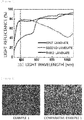
- FIG. 2 is a view illustrating the light reflectance of each of the first laminate, the second laminate, and the third laminate according to an exemplary embodiment of the present invention. Specifically, FIG. 2 illustrates the light reflectance of each of the first laminate composed of the first substrate and the first metal layer, the second laminate composed of the first substrate and the second metal layer, and the third laminate composed of the first substrate and the third metal layer.
- the first laminate composed of the first substrate and the first metal layer had a light reflectance of about 38% with respect to light having a wavelength value of 355 nm. Furthermore, it was confirmed that the second laminate composed of the first substrate and the second metal layer had a light reflectance of about 78.5% with respect to light having a wavelength value of 355 nm and the third laminate composed of the first substrate and the third metal layer had a light reflectance of about 76% with respect to light having a wavelength value of 355 nm.
- Example 1 of the present invention The surfaces of the amorphous layers produced in Example 1 of the present invention and Comparative Example 1 were observed by a scanning electron microscope (SU8020, HITACHI, Ltd.), and the SEM photographs thereof were captured.
- FIG. 3 is a set of scanning electron microscope (SEM) photographs of the surfaces of the amorphous layers produced in Example 1 of the present invention and Comparative Example 1.
- SEM scanning electron microscope
- the thickness of the multilayered metal layer by adjusting the thickness of the multilayered metal layer to 1.5 ⁇ m to 3.0 ⁇ m, the surface roughness of an amorphous layer to be formed can be reduced, and an amorphous layer having a homogenous composition can be formed.
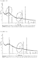
- amorphous layers produced in Examples 1 and 2 and Reference Examples 1 and 2 of the present invention were subjected to X-ray diffraction spectroscopy (XRD) analysis using an X-ray diffraction analyzer (D4 endeavor, Bruker Corporation).
- XRD X-ray diffraction spectroscopy
- FIG. 4A is a view illustrating X-ray diffraction spectroscopy (XRD) analysis results of the amorphous layer produced in Example 1 of the present invention
- FIG. 4B is a view illustrating XRD analysis results of the amorphous layer produced in Example 2 of the present invention
- FIG. 4C is a view illustrating XRD analysis results of the amorphous layer produced in Reference Example 1 of the present invention
- FIG. 4D is a view illustrating XRD analysis results of the amorphous layer produced in Reference Example 2 of the present invention
- FIG. 4E is a view illustrating XRD analysis results of the multilayered metal layer produced in Example 1 of the present invention.
- Example 1 it was confirmed that in the multilayered metal layer produced in Example 1 of the present invention, a peak exhibiting crystallinity was present.
- FIGS. 4A and 4B it was confirmed that in the case of Example 1 in which the scanning speed of the laser was adjusted to 2.5 mm/sec and Example 2 in which the scanning speed of the laser was adjusted to 5 mm/sec, the height of the peak exhibiting crystallinity was very low. That is, it was confirmed that through Examples 1 and 2, the amorphous layers having amorphous properties could be produced from the multilayered metal layer having crystallinity.
- Example 1 Mg Cu Sm (at%) (at%) (at%) Example 1 (Multilayered metal layer) 84.07 15.02 0.91
- FIG. 5 is a phase diagram illustrating the composition ranges of the multilayered metal layer and the amorphous layer produced in Example 1 of the present invention.
- FIG. 5 illustrates a phase diagram of the three elements of magnesium, copper, and samarium, and is a view illustrating an amorphous region and a crystalline region according to the contents of magnesium, copper, and samarium. More specifically, FIG. 5 is a view illustrating that the composition of the multilayered metal layer produced in Example 1 of the present invention is included in the crystalline region, and the composition of the amorphous layer is included in the amorphous region.
- Example 1 of the present invention had crystallinity, but the amorphous metal layer formed on one surface of the second substrate was in the amorphous form.
- the amorphous metal layer can be formed on one surface of the second substrate.
- the crystallinity of the amorphous layer transferred onto one surface of the second substrate can be effectively reduced by adjusting the scanning speed of the laser with which the multilayered metal layer is irradiated.
Landscapes
- Chemical & Material Sciences (AREA)
- Engineering & Computer Science (AREA)
- Chemical Kinetics & Catalysis (AREA)
- Organic Chemistry (AREA)
- Materials Engineering (AREA)
- Mechanical Engineering (AREA)
- Metallurgy (AREA)
- Physics & Mathematics (AREA)
- Optics & Photonics (AREA)
- General Chemical & Material Sciences (AREA)
- Life Sciences & Earth Sciences (AREA)
- Geochemistry & Mineralogy (AREA)
- Thermal Sciences (AREA)
- Plasma & Fusion (AREA)
- Inorganic Chemistry (AREA)
- Oil, Petroleum & Natural Gas (AREA)
- Toxicology (AREA)
- Health & Medical Sciences (AREA)
- Laminated Bodies (AREA)
- Physical Vapour Deposition (AREA)
- Electrodes Of Semiconductors (AREA)
- Internal Circuitry In Semiconductor Integrated Circuit Devices (AREA)
Abstract
Description
- The present invention relates to a method for producing an amorphous thin film capable of easily forming an amorphous layer by laser irradiation.
- An amorphous metal theoretically means a metal that does not have a grain boundary. Further, in general, the amorphous metal may have microcrystallinity, but has a short-range order, so that there is an advantage in that it is possible to reduce a phenomenon in which fracture occurs from the grain boundary, which is a position where defects are generated, when external force is applied. That is, the amorphous metal has an aspect in which mechanical properties are excellent as compared to a pure metal or alloy having crystallinity.
- In order to prepare an amorphous metal, generally, various metals of three more components are adjusted according to the composition, dissolved in a molten metal, and prepared as a bulk-type amorphous alloy. However, since each metal has a difference in melting temperature, it is difficult to uniformly control the composition in the melting process, thereby causing a problem in that a crystal phase is partially produced. The produced crystal phase is a main position where defects occur and becomes a starting point where cracks are generated by external force, thereby causing a problem in that the alloy is fractured by the cracks. In addition, since an amorphous alloy prepared by a method in the related art is not thick enough to be processed, there is a problem in that it is difficult to form the amorphous alloy in the form of a thin film.
- Therefore, there is a need for a technique capable of manufacturing an amorphous thin film having a homogeneous composition.
- Thus, the present invention has been made in an effort to provide a method for producing an amorphous thin film capable of easily producing an amorphous layer.
- However, a problem to be solved by the present invention is not limited to the aforementioned problem, and the other problems that are not mentioned may be clearly understood by a person skilled in the art from the following description.
- An exemplary embodiment of the present invention provides a method for producing an amorphous thin film, the method including: forming a multilayered metal layer in which a first metal layer, a second metal layer, and a third metal layer are sequentially provided by sequentially depositing a first metal, a second metal, and a third metal on one surface of a first substrate; positioning one surface of a second substrate so as to face the one surface of the first substrate; and forming an amorphous layer including the first metal, the second metal, and the third metal on the one surface of the second substrate by irradiating the first substrate with a laser in a direction from the other surface to the one surface of the first substrate.
- The method for producing an amorphous thin film according to an exemplary embodiment of the present invention may form an amorphous layer on a second substrate by a simple method of irradiating a multilayered metal layer provided on a first substrate with a laser.
- The effects of the present invention are not limited to the above-described effects, and effects, which are not mentioned, will be clearly understood by a person skilled in the art from the specification of the present application and the accompanying drawings.
-
-
FIG. 1 is a view illustrating a process of producing an amorphous thin film according to an exemplary embodiment of the present invention. -
FIG. 2 is a view illustrating the light reflectance of each of a first laminate, a second laminate, and a third laminate according to an exemplary embodiment of the present invention. -
FIG. 3 is a set of scanning electron microscope (SEM) photographs of the surfaces of amorphous layers produced in Example 1 of the present invention and Comparative Example 1. -
FIG. 4A is a view illustrating X-ray diffraction spectroscopy (XRD) analysis results of the amorphous layer produced in Example 1 of the present invention,FIG. 4B is a view illustrating XRD analysis results of the amorphous layer produced in Example 2 of the present invention,FIG. 4C is a view illustrating XRD analysis results of the amorphous layer produced in Reference Example 1 of the present invention,FIG. 4D is a view illustrating XRD analysis results of the amorphous layer produced in Reference Example 2 of the present invention, andFIG. 4E is a view illustrating XRD analysis results of the multilayered metal layer produced in Example 1 of the present invention. -
FIG. 5 is a phase diagram illustrating the composition ranges of the multilayered metal layer and the amorphous layer produced in Example 1 of the present invention. - Throughout the specification of the present application, when one part "includes" one constituent element, unless otherwise specifically described, this does not mean that another constituent element is excluded, but means that another constituent element may be further included.
- Throughout the specification of the present application, when one member is disposed "on" another member, this includes not only a case where the one member is brought into contact with another member, but also a case where still another member is present between the two members.
- Throughout the specification of the present application, a term for a degree used, such as a "step ..." or a "step of ...", does not mean a "step for ...".
- Throughout the specification of the present application, the unit "wt%" means a weight ratio of a component included in a member based on the total weight of the member.
- Throughout the specification of the present application, the unit "at%" means a percentage of the corresponding atom based on the total number of atoms included in a member.
- Throughout the specification of the present application, the "light reflectance" means a ratio of the amount of light reflected from a member to the amount of light incident to the member. In this case, the amount of light incident to the member and the amount of light reflected from the member may be measured using a spectrophotometer (Lambda 950, PerkinElmer, Inc.).
- Throughout the specification of the present application, the scanning speed of a laser means the speed at which the light source of the laser moves from one point on the surface of a member, which is irradiated with the laser, to the other point.
- Throughout the specification of the present application, the spot size of a laser means the distance from one end to the other end of the region which is irradiated with the laser.
- Throughout the specification of the present application, the pulse repetition rate of a laser means the frequency of the laser per second.
- Hereinafter, the present specification will be described in more detail.
- An exemplary embodiment of the present invention provides a method for producing an amorphous thin film, the method including: forming a multilayered metal layer in which a first metal layer, a second metal layer, and a third metal layer are sequentially provided by sequentially depositing a first metal, a second metal, and a third metal on one surface of a first substrate; positioning one surface of a second substrate so as to face the one surface of the first substrate; and forming an amorphous layer including the first metal, the second metal, and the third metal on the one surface of the second substrate by irradiating the first substrate with a laser in a direction from the other surface to the one surface of the first substrate.
- The method for producing an amorphous thin film according to an exemplary embodiment of the present invention may form an amorphous layer on the second substrate by a simple method of irradiating the multilayered metal layer provided on the first substrate with the laser. Specifically, an amorphous layer may be easily transferred onto one surface of the second substrate by irradiating the multilayered metal layer having crystallinity with the laser.
-
FIG. 1 is a view illustrating a process of producing an amorphous thin film according to an exemplary embodiment of the present invention. Specifically,FIG. 1 illustrates that amultilayered metal layer 200 is formed in which afirst metal layer 210, asecond metal layer 220, and athird metal layer 230 are sequentially laminated on one surface of afirst substrate 100 by sequentially depositing a first metal, a second metal, and a third metal on the one surface of thefirst substrate 100. Further,FIG. 1 illustrates that anamorphous layer 400 including a first metal, a second metal, and a third metal is transferred onto one surface of asecond substrate 300 by irradiating thefirst substrate 100, having themultilayered metal layer 200 formed on the one surface thereof, with a laser L in a direction from the other surface to the one surface of thefirst substrate 100. - According to an exemplary embodiment of the present invention, the light reflectance of the first substrate may be 1 % to 40 %. Specifically, the first substrate may have a light reflectance of 1% to 40% with respect to light having a wavelength value of any one wavelength value of the wavelengths from 100 nm to 1,064 nm. More specifically, the light reflectance of the first substrate may be a light reflectance with respect to light having a wavelength value of 355 nm. The light reflectance of the first substrate may be, for example, a light reflectance of 30% with respect to light having a wavelength value of 355 nm. By using the first substrate having the light reflectance within the above-described range, the laser with which the first substrate is irradiated in a direction form the other surface to the one surface of the first substrate may effectively reach the multilayered metal layer.
- According to an exemplary embodiment of the present invention, as the first substrate, any substrate may be used without limitation as long as the substrate has the above-described light reflectance. Specifically, as the first substrate, it is possible to use a substrate which facilitates the transmission of a laser beam in the wavelength range of the laser beam used to transfer a multilayered metal layer. For example, as the first substrate, it is possible to use a glass substrate, a polyethylene terephthalate (PET) substrate, a polyimide (PI) substrate, and the like, but the type of first substrate is not limited.
- According to an exemplary embodiment of the present invention, the first substrate may have a thickness of 0.1 mm to 2.0 mm. For example, the substrate may have a thickness of 0.1 mm to 1.0 mm, or 1.0 mm to 2.0 mm. The laser with which the first substrate is irradiated may be effectively induced on the multilayered metal layer by adjusting the thickness of the first substrate within the above-described range. In addition, when the thickness of the first substrate is within the above-described range, the first substrate may be suppressed from being deformed by the laser. Accordingly, it is possible to prevent the laser process efficiency from deteriorating.
- According to an exemplary embodiment of the present invention, any substrate used in the art may be used without limitation as the second substrate. Furthermore, the type of second substrate may be selected according to the purpose for which the second substrate provided with the amorphous layer is used. For example, when the amorphous layer is applied to a solar cell electrode, as the second substrate, it is possible to use a soda lime glass substrate, a ceramic substrate such as alumina and quartz, and a metal substrate such as stainless steel, chrome steel, titanium, ferrite steel, and molybdenum.
- Further, the first substrate and the second substrate may be formed of the same material or different materials.
- According to an exemplary embodiment of the present invention, the deposition of the metal may be performed by any one method of sputtering, an electron beam deposition method, a thermal deposition method, a plasma chemical vapor deposition method, and a low-pressure chemical vapor deposition method. That is, the deposition of the first metal, the second metal, and the third metal may be performed by any one method of sputtering, an electron beam deposition method, a thermal deposition method, a plasma chemical vapor deposition method, and a low-pressure chemical vapor deposition method. Specifically, it is possible to form a first metal layer, a second metal layer, and a third metal layer having a homogenous composition on one surface of the first substrate by using a sputtering method to sequentially deposit a first metal, a second metal, and a third metal on the one surface of the first substrate. Further, when the sputtering method is used, it is possible to easily adjust the thicknesses of the first metal layer, the second metal layer, and the third metal layer to be formed on the one surface of the first substrate by adjusting a sputtering power, an angle and a distance between a sputtering target and the first substrate, and the like.
- According to an exemplary embodiment of the present invention, a light reflectance of the first metal layer may be smaller than the light reflectance of each of the second metal layer and the third metal layer. Specifically, with respect to light having any one wavelength value of the wavelengths from 100 nm to 1,064 nm, the light reflectance of the first metal layer may be smaller than the light reflectance of the second metal layer and the light reflectance of the third metal layer. More specifically, the light reflectance of each of the first metal layer, the second metal layer, and the third metal layer may be a light reflectance with respect to light having any one wavelength value of the wavelengths from 300 nm to 450 nm, and more specifically, may be a light reflectance with respect to light having a wavelength value of 355 nm.
- Referring to
FIG. 1 , thefirst substrate 100 is irradiated with the laser L in a direction from the other surface to the one surface of thefirst substrate 100 and the laser L is brought into first contact with thefirst metal layer 210 in themultilayered metal layer 200. Thus, it is possible to effectively prevent the transfer efficiency from the multilayered metal layer to the amorphous layer from deteriorating by providing the first metal layer having the lowest light reflectance adjacent to the one surface of the first substrate. Specifically, the degree of reflection of the laser beam incident to the first metal layer having the lowest light reflectance is reduced by causing the laser to reach the first metal layer first, thereby preventing the laser process efficiency from deteriorating. - According to an exemplary embodiment of the present invention, the light reflectance of each of the first metal layer, the second metal layer, and the third metal layer may be measured by providing the first metal layer, the second metal layer, and the third metal layer on the first substrate. For example, it is possible to measure the light reflectance of a first laminate composed of the first substrate and the first metal layer provided on the first substrate. Further, it is possible to measure the light reflectance of a second laminate composed of the first substrate and the second metal layer provided on the first substrate, and to measure the light reflectance of a third laminate composed of the first substrate and the third metal layer provided on the first substrate.
- According to an exemplary embodiment of the present invention, the laminate composed of the first metal layer and the first substrate may have a light reflectance of 45% or less. Specifically, the laminate composed of the first metal layer and the first substrate may have a light reflectance of 1% to 45%, 5% to 40%, 10% to 30%, 15% to 30%, 35% to 45%, 35% to 38%, 38% to 45%, or 38 %. Further, the light reflectance of the laminate may be a reflectance with respect to light having any one wavelength value of the wavelengths from 100 nm to 1,064 nm, or the wavelengths from 300 nm to 450 nm. More specifically, the light reflectance of the laminate may be a light reflectance with respect to light having a wavelength value of 355 nm. When the light reflectance of the laminate composed of the first substrate and the first metal layer is within the above-described range, it is possible to effectively prevent the transfer efficiency from the multilayered metal layer to the amorphous layer from deteriorating.
- According to an exemplary embodiment of the present invention, among the melting points of the first metal layer to the third metal layer, the difference between the highest melting point value and the lowest melting point value may be 200°C to 500°C. Specifically, the difference in melting point between the metal layer having the highest melting point and the metal layer having the lowest melting point may be 400°C to 450°C, 400°C to 435°C, 435°C to 450°C, 430°C to 440°C, 280°C to 450°C, 300°C to 400°C, 200°C to 270°C, or 310°C to 470°C. When the difference between the highest melting point value and the lowest melting point value is within the above-described range among the melting points of the first metal layer to the third metal layer, the laser process efficiency may be improved. Specifically, by adjusting the difference between the highest melting point value and the lowest melting point value within the above-described range, it is possible to decrease the amount of energy for transferring the multilayered metal layer and to suppress a multilayered metal layer from being evaporated. Accordingly, it is possible to effectively prevent a crystal phase from being formed on an amorphous layer as the multilayered metal layer is rapidly evaporated and solidified.
- In addition, the first metal layer may have the highest melting point, and the third metal layer may have the lowest melting point.
- According to an exemplary embodiment of the present invention, the difference between the melting point of the first metal layer and the melting point of the second metal layer may be 10°C to 100°C. For example, the difference may be 10°C to 13°C. Furthermore, the difference between the melting point of the second metal layer and the melting point of the third metal layer may be 100°C to 450°C. For example, the difference may be 100°C to 422°C, or 422°C to 450°C. The laser process efficiency may be effectively suppressed from deteriorating by adjusting the difference between the melting points of the metal layers within the above-described range.
- Further, according to an exemplary embodiment of the present invention, the third metal layer may have a melting point of 500°C to 900°C. For example, the melting point may be 500°C to 650°C, 650°C to 900°C, 600°C to 650°C, or 650°C to 700°C. The transfer efficiency of a multilayered metal layer may be improved by adjusting the melting point of the third metal layer within the above-described range. When the melting point of the third metal layer is within the above-described range, the third metal layer provided at a position where the laser reaches last may also be easily melted and thus transferred onto one surface of the second substrate.
- According to an exemplary embodiment of the present invention, the atomic radii of the first metal, the second metal, and the third metal are different from one another. Further, the types of first metal, second metal, and third metal may be selected by considering the atomic radii of the first metal, the second metal, and the third metal so as to implement amorphous properties of the amorphous layer.
- According to an exemplary embodiment of the present invention, the third metal may include at least one of magnesium, calcium, aluminum, and lanthanum. In addition, the first metal may include at least one of copper, yttrium, and silver. Furthermore, the second metal may include at least one of samarium and neodymium. However, the types of first metal, second metal, and third metal are not limited, and it is possible to select and use an appropriate metal element capable of implementing physical properties of the amorphous layer as the first metal to the third metal.
- An amorphous layer may be formed on one surface of the second substrate by appropriately selecting the types of first metal, second metal, and third metal. For example, a multilayered metal layer may be produced by forming a first metal layer including copper on one surface of the first substrate, forming a second metal layer including samarium on the first metal layer, and forming a third metal layer including magnesium on the second metal layer, and an amorphous layer may be formed on one surface of the second substrate by irradiating the multilayered metal layer with the laser.
- According to an exemplary embodiment of the present invention, the multilayered metal layer may have a thickness of 1.5 µm to 3.0 µm. Specifically, the multilayered metal layer may have a thickness of 1.7 µm to 2.8 µm, 2.0 µm to 2.5 µm, 1.5 µm to 1.8 µm, or 2.1 µm to 2.7 µm. An amorphous layer may be easily formed by adjusting the thickness of the multilayered metal layer within the above-described range to improve the transfer efficiency of the multilayered metal layer. Further, when the thickness of the multilayered metal layer is within the above-described range, the surface roughness of an amorphous layer to be formed on one surface of the second substrate may be effectively reduced, and the composition of the amorphous layer may be effectively homogenized.
- According to an exemplary embodiment of the present invention, a multilayered metal layer provided on one surface of the first substrate may be transferred onto one surface of the second substrate by irradiating the first substrate, in which the multilayered metal layer formed on one surface thereof, with the laser in a direction from the other surface of the first substrate to the one surface of the first substrate, thereby forming an amorphous layer. Specifically, when the laser is incident to the multilayered metal layer, the multilayered metal layer is melted and thus transferred onto one surface of the second substrate, and as the metal layer is rapidly cooled, an amorphous layer may be formed on one surface of the second substrate.
- According to an exemplary embodiment of the present invention, it is possible to suppress a large amount of evaporation generated during the process in which the multilayered metal layer is transferred, by adjusting the difference among the melting points of the first metal layer to the third metal layer and/or the thickness of the multilayered metal layer. Specifically, by suppressing the evaporation phenomenon, it is possible to prevent a crystal phase from being formed due to the composition imbalance of the amorphous layer. In addition, it is possible to suppress the transfer efficiency of the multilayered metal layer from deteriorating due to the evaporated component precipitated in the form of a powder on the second substrate as the evaporated component is rapidly cooled.
- According to an exemplary embodiment of the present invention, a laser used in the art may be used, and specifically, a pulse laser may be used. More specifically, as the laser, a pulse laser with a wavelength of 355 nm may be used. In addition, the laser may have an output of 1 W/cm2 to 10 W/cm2. Specifically, the laser may have an output of 1.5 W/cm2 to 8 W/cm2, 1.5 W/cm2 to 8 W/cm2, 2 W/cm2 to 6 W/cm2, 2.5 W/cm2 to 4.5 W/cm2, 1 W/cm2 to 2 W/cm2, or 4 W/cm2 to 8 W/cm2. Energy may be stably transferred to the multilayered metal layer by adjusting the output of the laser within the above-described range.
- According to an exemplary embodiment of the present invention, the laser irradiation may be performed at a scanning speed of 1 mm/sec to 20 mm/sec. Specifically, the laser irradiation may be performed at a scanning speed of 2 mm/sec to 18 mm/sec, 4.5 mm/sec to 15 mm/sec, 7 mm/sec to 12.5 mm/sec, 1.5 mm/sec to 5 mm/sec, 8 mm/sec to 13 mm/sec, or 15 mm/sec to 19 mm/sec, at an output of 2 W/cm2. More specifically, the scanning speed of the laser may be 1 mm/sec to 5 mm/sec, 1.5 mm/sec to 4.5 mm/sec, 2.0 mm/sec to 3.5 mm/sec, 1.0 mm/sec to 2.5 mm/sec, 2.5 mm/sec to 5.0 mm/sec, 2.5 mm/sec to 10 mm/sec, 2.5 mm/sec to 20.0 mm/sec, 5.0 mm/sec to 10 mm/sec, 5.0 mm/sec to 20 mm/sec, or 3.0 mm/sec to 5.0 mm/sec. The crystallinity of the amorphous layer transferred onto one surface of the second substrate may be effectively reduced by adjusting the scanning speed of the laser within the above-described range.
- According to an exemplary embodiment of the present invention, the laser may have a pulse repetition rate of 1 kHz to 40 kHz. Specifically, the laser may have a pulse repetition rate of 3 kHz to 35 kHz, 5 kHz to 30 kHz, 10 kHz to 20 kHz, or 13 kHz to 17 kHz. More specifically, the laser may have a pulse repetition rate of 25 kHz to 35 kHz, or 30 kHz to 40 kHz. For example, the laser may have a pulse repetition rate of 30 kHz. By adjusting the pulse repetition rate of the laser within the above-described range, it is possible to suppress the laser process efficiency from deteriorating due to the reduction in degree of superposition of the focused laser beam.
- Furthermore, when the pulse repetition rate of the laser is within the above-described range, it is possible to prevent the first substrate from being degraded by irradiation with excess energy.
- According to an exemplary embodiment of the present invention, the laser irradiation may be performed with a spot size of 10 µm to 200 µm. Specifically, the laser irradiation may be performed with a spot size of 20 µm to 180 µm, 40 µm to 160 µm, or 70 µm to 120 µm. More specifically, the laser irradiation may be performed with a spot size of 15 µm to 40 µm, 20 µm to 30 µm, or 25 µm to 30 µm. For example, the spot size may be 25 µm. By adjusting the spot size of the laser within the above-described range, it is possible to suppress the first substrate from being thermally deformed by the laser. Further, when the spot size of the laser is within the above-described range, it is possible to suppress the laser process from becoming unstable due to the decrease in the superposition rate of the laser spot.
- According to an exemplary embodiment of the present invention, the output, scanning speed, and pulse repetition rate of the laser interact with each other, and process conditions of the laser may be controlled by adjusting at least one of the output, scanning speed, and pulse repetition rate of the laser. Further, according to the object to be irradiated with laser, the object may also be irradiated by adjusting the output, scanning speed, pulse repetition rate, and spot size of the laser out of the above-described range.
- According to an exemplary embodiment of the present invention, the amorphous layer may have a thickness of 0.01 µm to 3 µm. Specifically, the amorphous layer may have a thickness of 0.01 µm to 1.4 µm, 1.4 µm to 3.0 µm, 0.05 µm to 2.8 µm, 0.1 µm to 2.0 µm, 0.5 µm to 1.8 µm, 1.0 µm to 1.5 µm, 0.2 µm to 0.7 µm, 1.2 µm to 1.7 µm, or 2.1 µm to 2.5 µm. For example, the thickness may be 1.4 µm. The thickness of the amorphous layer may be controlled by adjusting the thickness of the multilayered metal layer, the output of the laser, and the like.
- Accordingly, the method for producing an amorphous thin film according to an exemplary embodiment of the present invention may easily form an amorphous metal layer in the form of a thin film on one surface of the second substrate.
- Hereinafter, the present invention will be described in detail with reference to Examples for specifically describing the present invention. However, the Examples according to the present invention may be modified in various forms, and it is not interpreted that the scope of the present invention is limited to the Examples to be described below. The Examples of the present specification are provided for more completely explaining the present invention to a person with ordinary skill in the art.
- As a first substrate, a glass substrate having a thickness of about 1 mm and a light reflectance of about 30% with respect to light having a wavelength value of 355 nm was prepared. Further, as a second substrate, a glass substrate having a thickness of about 1 mm was prepared. Thereafter, a first metal layer having a thickness of about 0.45 µm was formed on one surface of the first substrate by setting an output of a sputtering device at 250 W/cm2 and sputtering a copper target at a
DC 1 cathode of the sputtering device. Thereafter, a second metal layer having a thickness of about 0.15 µm was formed on the first metal layer by setting the output of the sputtering device at 25 W/cm2 and sputtering samarium at an RF cathode of the sputtering device. Thereafter, a third metal layer having a thickness of about 0.90 µm was formed on the second metal layer by setting the output of the sputtering device at 300 W/cm2 and sputtering a magnesium target at aDC 2 cathode of the sputtering device. Accordingly, a multilayered metal layer having a total thickness of about 1.5 µm was formed on one surface of the first substrate. - The second substrate was positioned so as to face the third metal layer. Thereafter, the first substrate was irradiated with a pulse laser having a wavelength of 355 nm, of which the output, the scanning speed, the spot size and the pulse repetition rate were set to 2 W/cm2, 2.5 mm/sec, 25 µm and 30 kHz, respectively, in a direction from the other surface to one surface thereof. Accordingly, an amorphous layer having a thickness of about 1.4 µm was formed on one surface of the second substrate.
- An amorphous layer was formed in the same manner as in Example 1, except that the scanning speed of the laser was adjusted to 5 mm/sec.
- An amorphous layer was formed in the same manner as in Example 1, except that a first metal layer having a thickness of about 0.99 µm was formed on a first substrate by setting an output of a sputtering device at 125 W/cm2 to sputter a copper target, a second metal layer having a thickness of about 0.33 µm was formed on the first metal layer by setting the output of the sputtering device at 50 W/cm2 to sputter a samarium target, and a third metal layer having a thickness of about 1.98 µm was formed on the second metal layer by setting the output of the sputtering device at 250 W/cm2 to sputter a magnesium target, thereby forming a multilayered metal layer having a total thickness of about 3.3 µm on one surface of the first substrate.
- An amorphous layer was formed in the same manner as in Example 1, except that the scanning speed of the laser was adjusted to 20 mm/sec.
- An amorphous layer was formed in the same manner as in Example 1, except that the scanning speed of the laser was adjusted to 10 mm/sec.
- The melting points of the first metal layer, the second metal layer, and the third metal layer produced in Example 1 were measured, and as a result, the melting point of the first metal layer was about 1,085°C, the melting point of the second metal layer was about 1,072°C, and the melting point of the third metal layer was about 650°C.
- The light reflectance of each of the first metal layer, the second metal layer, and the third metal layer was measured as described below. A glass substrate having a thickness of about 1 mm and a light reflectance of about 30% with respect to light having a wavelength value of 355 nm was prepared, and a first metal layer having a thickness of about 0.45 µm on a glass substrate was formed by setting the output of the sputtering device at 250 W/cm2, and sputtering a copper target at a
DC 1 cathode of the sputtering device, thereby producing a first laminate. Further, A second metal layer having a thickness of about 0.15 µm was formed on another glass substrate by setting the output of the sputtering device at 25 W/cm2 and sputtering samarium at an RF cathode of the sputtering device, thereby producing a second laminate. In addition, a third metal layer having a thickness of about 0.90 µm was formed on still another glass substrate by setting the output of the sputtering device at 300 W/cm2 and sputtering a magnesium target at aDC 2 cathode of the sputtering device, thereby producing a third laminate. - Thereafter, the light reflectance of each of the first laminate, the second laminate, and the third laminate was measured using a spectrophotometer (Lambda 950, PerkinElmer Inc.).
-
FIG. 2 is a view illustrating the light reflectance of each of the first laminate, the second laminate, and the third laminate according to an exemplary embodiment of the present invention. Specifically,FIG. 2 illustrates the light reflectance of each of the first laminate composed of the first substrate and the first metal layer, the second laminate composed of the first substrate and the second metal layer, and the third laminate composed of the first substrate and the third metal layer. - Referring to
FIG. 2 , it was confirmed that the first laminate composed of the first substrate and the first metal layer had a light reflectance of about 38% with respect to light having a wavelength value of 355 nm. Furthermore, it was confirmed that the second laminate composed of the first substrate and the second metal layer had a light reflectance of about 78.5% with respect to light having a wavelength value of 355 nm and the third laminate composed of the first substrate and the third metal layer had a light reflectance of about 76% with respect to light having a wavelength value of 355 nm. - The surfaces of the amorphous layers produced in Example 1 of the present invention and Comparative Example 1 were observed by a scanning electron microscope (SU8020, HITACHI, Ltd.), and the SEM photographs thereof were captured.
-
FIG. 3 is a set of scanning electron microscope (SEM) photographs of the surfaces of the amorphous layers produced in Example 1 of the present invention and Comparative Example 1. Referring toFIG. 3 , it was confirmed that in the case of Example 1 in which the thickness of the multilayered metal layer was adjusted to about 2.5 µm, the surface of the amorphous layer formed as the multilayered metal layer was transferred was smooth, and the amorphous metal layer was formed with a homogenous composition on the surface. Meanwhile, it was confirmed that in the case of Comparative Example 1 in which the thickness of the multilayered metal layer was adjusted to about 3.3 µm, the surface of the amorphous layer was a little rough and the amorphous metal layer on the surface was not homogenous. - Accordingly, it can be seen that according to an exemplary embodiment of the present invention, by adjusting the thickness of the multilayered metal layer to 1.5 µm to 3.0 µm, the surface roughness of an amorphous layer to be formed can be reduced, and an amorphous layer having a homogenous composition can be formed.
- The amorphous layers produced in Examples 1 and 2 and Reference Examples 1 and 2 of the present invention were subjected to X-ray diffraction spectroscopy (XRD) analysis using an X-ray diffraction analyzer (D4 endeavor, Bruker Corporation).
-
FIG. 4A is a view illustrating X-ray diffraction spectroscopy (XRD) analysis results of the amorphous layer produced in Example 1 of the present invention,FIG. 4B is a view illustrating XRD analysis results of the amorphous layer produced in Example 2 of the present invention,FIG. 4C is a view illustrating XRD analysis results of the amorphous layer produced in Reference Example 1 of the present invention,FIG. 4D is a view illustrating XRD analysis results of the amorphous layer produced in Reference Example 2 of the present invention, andFIG. 4E is a view illustrating XRD analysis results of the multilayered metal layer produced in Example 1 of the present invention. - Referring to
FIG. 4E , it was confirmed that in the multilayered metal layer produced in Example 1 of the present invention, a peak exhibiting crystallinity was present. Meanwhile, referring toFIGS. 4A and 4B , it was confirmed that in the case of Example 1 in which the scanning speed of the laser was adjusted to 2.5 mm/sec and Example 2 in which the scanning speed of the laser was adjusted to 5 mm/sec, the height of the peak exhibiting crystallinity was very low. That is, it was confirmed that through Examples 1 and 2, the amorphous layers having amorphous properties could be produced from the multilayered metal layer having crystallinity. - Meanwhile, it was confirmed that in the case of Reference Example 1 in which the scanning speed of the laser was adjusted to 20 mm/sec and Reference Example 2 in which the scanning speed of the laser was adjusted to 10 mm/sec, peaks exhibiting crystallinity somewhat appeared. Furthermore, it was confirmed that in the case of Example 1, a peak exhibiting crystallinity rarely appeared as compared to Example 2.
- Further, the contents of magnesium, copper, and samarium, which are included in the multilayered metal layer produced in Example 1 of the present invention and the amorphous layer produced in Example 1 and obtained through the XRD analysis, are shown in the following Table 1.
[Table 1] Mg Cu Sm (at%) (at%) (at%) Example 1 (Multilayered metal layer) 84.07 15.02 0.91 Example 1 (Amorphous layer) 60 30 10 -
FIG. 5 is a phase diagram illustrating the composition ranges of the multilayered metal layer and the amorphous layer produced in Example 1 of the present invention. Specifically,FIG. 5 illustrates a phase diagram of the three elements of magnesium, copper, and samarium, and is a view illustrating an amorphous region and a crystalline region according to the contents of magnesium, copper, and samarium. More specifically,FIG. 5 is a view illustrating that the composition of the multilayered metal layer produced in Example 1 of the present invention is included in the crystalline region, and the composition of the amorphous layer is included in the amorphous region. - Referring to Table 1 and
FIG. 5 , it was confirmed that the multilayered metal layer formed in Example 1 of the present invention had crystallinity, but the amorphous metal layer formed on one surface of the second substrate was in the amorphous form. - Therefore, according to an exemplary embodiment of the present invention, it can be seen that through a simple method of irradiating the multilayered metal layer having crystallinity with the laser, the amorphous metal layer can be formed on one surface of the second substrate. In addition, it can be seen that the crystallinity of the amorphous layer transferred onto one surface of the second substrate can be effectively reduced by adjusting the scanning speed of the laser with which the multilayered metal layer is irradiated.
-
- 100:
- First substrate
- 200:
- Multilayered metal layer
- 210:
- First metal layer
- 220:
- Second metal layer
- 230:
- Third metal layer
- 300:
- Second substrate
- 400:
- Amorphous layer
Claims (11)
- A method for producing an amorphous thin film, the method comprising:forming a multilayered metal layer in which a first metal layer, a second metal layer, and a third metal layer are sequentially provided by sequentially depositing a first metal, a second metal, and a third metal on one surface of a first substrate;positioning one surface of a second substrate so as to face the one surface of the first substrate; andforming an amorphous layer comprising the first metal, the second metal, and the third metal on the one surface of the second substrate by irradiating the first substrate with a laser in a direction from the other surface to the one surface of the first substrate.
- The method of claim 1, wherein the deposition of the metal is performed by any one method of sputtering, an electron beam deposition method, a thermal deposition method, a plasma chemical vapor deposition method, and a low-pressure chemical vapor deposition method.
- The method of claim 1, wherein a light reflectance of the first metal layer is smaller than a light reflectance of each of the second metal layer and the third metal layer.
- The method of claim 1, wherein a laminate composed of the first metal layer and the first substrate has a light reflectance of 45% or less.
- The method of claim 1, wherein among the melting points of the first metal layer to the third metal layer, a difference between the highest melting point value and the lowest melting point value is 200°C to 500°C.
- The method of claim 1, wherein the multilayered metal layer has a thickness of 1.5 µm to 3.0 µm.
- The method of claim 1, wherein the laser irradiation is performed at an output of 1 W/cm2 to 10 W/cm2.
- The method of claim 1, wherein the laser irradiation is performed at a scanning speed of 1 mm/sec to 20 mm/sec.
- The method of claim 1, wherein the laser irradiation is performed with a spot size of 10 µm to 200 µm.
- The method of claim 1, wherein the laser has a pulse repetition rate of 1 kHz to 40 kHz.
- The method of claim 1, wherein the amorphous layer has a thickness of 0.01 µm to 3 µm.
Applications Claiming Priority (2)
| Application Number | Priority Date | Filing Date | Title |
|---|---|---|---|
| KR1020180068864A KR102391800B1 (en) | 2018-06-15 | 2018-06-15 | Manufacturing method for amorphous thin film |
| PCT/KR2019/006981 WO2019240455A1 (en) | 2018-06-15 | 2019-06-11 | Method for manufacturing amorphous thin film |
Publications (3)
| Publication Number | Publication Date |
|---|---|
| EP3719170A1 true EP3719170A1 (en) | 2020-10-07 |
| EP3719170A4 EP3719170A4 (en) | 2021-04-21 |
| EP3719170B1 EP3719170B1 (en) | 2022-02-23 |
Family
ID=68843317
Family Applications (1)
| Application Number | Title | Priority Date | Filing Date |
|---|---|---|---|
| EP19818822.9A Active EP3719170B1 (en) | 2018-06-15 | 2019-06-11 | Method for manufacturing amorphous thin film |
Country Status (6)
| Country | Link |
|---|---|
| US (1) | US11680311B2 (en) |
| EP (1) | EP3719170B1 (en) |
| JP (1) | JP7077518B2 (en) |
| KR (1) | KR102391800B1 (en) |
| CN (1) | CN111566258A (en) |
| WO (1) | WO2019240455A1 (en) |
Families Citing this family (2)
| Publication number | Priority date | Publication date | Assignee | Title |
|---|---|---|---|---|
| CN113871361B (en) * | 2021-09-26 | 2025-04-04 | 臻驱科技(上海)股份有限公司 | A semiconductor module substrate and design method |
| CN116002991B (en) * | 2023-02-10 | 2023-07-04 | 广东工业大学 | A multi-layer composite film and its application in laser precision forming |
Family Cites Families (25)
| Publication number | Priority date | Publication date | Assignee | Title |
|---|---|---|---|---|
| JPS5513945A (en) * | 1978-07-17 | 1980-01-31 | Seiko Epson Corp | Amorphous semiconductor device |
| AU7923287A (en) * | 1986-09-30 | 1988-04-14 | Kuroki Kogyosho Co., Ltd. | Method for producing amorphous metal layer |
| US4970196A (en) * | 1987-01-15 | 1990-11-13 | The Johns Hopkins University | Method and apparatus for the thin film deposition of materials with a high power pulsed laser |
| KR940004641B1 (en) | 1989-11-25 | 1994-05-27 | 삼성코닝 주식회사 | Single Crystal Manufacturing Equipment |
| JPH0690976B2 (en) * | 1990-10-05 | 1994-11-14 | インターナショナル・ビジネス・マシーンズ・コーポレーション | Magneto-optical recording medium |
| JPH0565671A (en) * | 1991-09-04 | 1993-03-19 | Nippondenso Co Ltd | Laminated structural body having amorphous alloy layer and its production |
| JP2002231628A (en) | 2001-02-01 | 2002-08-16 | Sony Corp | Method for forming semiconductor thin film, method for manufacturing semiconductor device, apparatus used for implementing these methods, and electro-optical device |
| KR100806137B1 (en) * | 2002-06-05 | 2008-02-22 | 주식회사 하이닉스반도체 | Method for fabricating semiconductor device having amorphous-metal gate electrode |
| US7951632B1 (en) * | 2005-01-26 | 2011-05-31 | University Of Central Florida | Optical device and method of making |
| CN101384952B (en) * | 2006-02-09 | 2010-08-25 | 旭硝子株式会社 | Optical component and manufacturing method thereof |
| US7927454B2 (en) * | 2007-07-17 | 2011-04-19 | Samsung Mobile Display Co., Ltd. | Method of patterning a substrate |
| JP2009242900A (en) * | 2008-03-31 | 2009-10-22 | National Institute Of Advanced Industrial & Technology | Method of manufacturing oxide layer |
| KR101222489B1 (en) * | 2011-03-09 | 2013-01-15 | 한국기계연구원 | Method for Wafer Dicing and Drilling through Anisotropic Etching after Local Amorphization using Laser Beam |
| KR20130026671A (en) | 2011-09-06 | 2013-03-14 | 엘지디스플레이 주식회사 | Crystallization method and method for manufacturing display device using the same |
| WO2013118201A1 (en) | 2012-02-08 | 2013-08-15 | 日本曹達株式会社 | Organic-inorganic composite thin film |
| ES2471568B1 (en) * | 2012-11-22 | 2015-08-21 | Abengoa Solar New Technologies S.A. | Procedure for creating electrical contacts and contacts thus created |
| JP5392932B2 (en) | 2012-12-21 | 2014-01-22 | 学校法人 東洋大学 | Method for producing amorphous carbon thin film |
| KR101476726B1 (en) | 2013-02-01 | 2014-12-30 | 한양대학교 산학협력단 | Method for coating amorphous thin film |
| CN105705671B (en) * | 2013-10-14 | 2019-10-29 | 奥宝科技股份有限公司 | The LIFT of more composition material structures prints |
| EP2974812B1 (en) | 2014-07-15 | 2019-09-04 | Heraeus Holding GmbH | Method for the manufacture of a component from a metal alloy with an amorphous phase |
| US9925797B2 (en) | 2014-08-07 | 2018-03-27 | Orbotech Ltd. | Lift printing system |
| KR101987263B1 (en) * | 2015-08-13 | 2019-06-10 | 주식회사 엘지화학 | Conductive structure body and method for manufacturing the same |
| KR101997661B1 (en) * | 2015-10-27 | 2019-07-08 | 주식회사 엘지화학 | Conductive structure body, electrode and display device comprising the same |
| KR20170097420A (en) | 2016-02-18 | 2017-08-28 | 주식회사 엘지화학 | Apparatus for manufacturing amorphous metal using 3D printer and amorphous metal |
| TW202224211A (en) * | 2016-03-31 | 2022-06-16 | 美商伊雷克托科學工業股份有限公司 | Methods of laser-seeding for electro-conductive plating |
-
2018
- 2018-06-15 KR KR1020180068864A patent/KR102391800B1/en active Active
-
2019
- 2019-06-11 US US16/969,809 patent/US11680311B2/en active Active
- 2019-06-11 JP JP2020535213A patent/JP7077518B2/en active Active
- 2019-06-11 WO PCT/KR2019/006981 patent/WO2019240455A1/en not_active Ceased
- 2019-06-11 CN CN201980007566.8A patent/CN111566258A/en active Pending
- 2019-06-11 EP EP19818822.9A patent/EP3719170B1/en active Active
Also Published As
| Publication number | Publication date |
|---|---|
| US20200370164A1 (en) | 2020-11-26 |
| JP2021509537A (en) | 2021-03-25 |
| KR20190141973A (en) | 2019-12-26 |
| JP7077518B2 (en) | 2022-05-31 |
| WO2019240455A1 (en) | 2019-12-19 |
| EP3719170B1 (en) | 2022-02-23 |
| KR102391800B1 (en) | 2022-04-29 |
| CN111566258A (en) | 2020-08-21 |
| US11680311B2 (en) | 2023-06-20 |
| EP3719170A4 (en) | 2021-04-21 |
Similar Documents
| Publication | Publication Date | Title |
|---|---|---|
| US5432151A (en) | Process for ion-assisted laser deposition of biaxially textured layer on substrate | |
| US6770154B2 (en) | Textured-grain-powder metallurgy tantalum sputter target | |
| US7081148B2 (en) | Textured-grain-powder metallurgy tantalum sputter target | |
| TWI616549B (en) | High rate deposition systems and processes for forming hermetic barrier layers | |
| EP3719170B1 (en) | Method for manufacturing amorphous thin film | |
| WO2008048628A2 (en) | Aligned crystalline semiconducting film on a glass substrate and methods of making | |
| Adurodija et al. | Effects of stress on the structure of indium-tin-oxide thin films grown by pulsed laser deposition | |
| US10174420B2 (en) | Method for forming oxide layer, laminated substrate for epitaxial growth, and method for producing the same | |
| Abegunde et al. | Surface integrity of TiC thin film produced by RF magnetron sputtering | |
| BE1030855B1 (en) | Conductive sputtering target and method for depositing a layer with it | |
| JP7820493B2 (en) | Method for manufacturing a solid-state component, solid-state component, quantum component, and apparatus for manufacturing a solid-state component | |
| US20210124252A1 (en) | Extreme ultraviolet mask blank defect reduction methods | |
| US12559834B2 (en) | Thermally stable metallic glass films via steep compositional gradients | |
| Nakamura et al. | Variation in 111 d-space and generation of hillocks in platinum thin-film electrodes by heat treatment | |
| Li et al. | Microstructure, Sputtering Performance, and Film Properties of Ag-1wt.% Cu Alloy Targets: A Comparative Study with Pure Ag | |
| JPH04182317A (en) | Method for producing oxide superconducting thin film | |
| Vu et al. | Physical Vapor Deposition and its application in vanadium dioxide synthesis | |
| JP2687845B2 (en) | Method for producing composite material thin film using pulsed laser deposition method | |
| Krebs et al. | Pulsed Laser Deposition of Thin Metallic Multilayers and Amorphous Films | |
| JP2024175910A (en) | Gallium nitride film deposition sputtering target | |
| KR20060054074A (en) | Laminate for Aluminum-Neodymium Alloy Sputtering | |
| JPS61170561A (en) | High melting point metal film forming method | |
| Marinov | Morphology and structure of gold, silver and copper layers obtained by sputtering during ion bombardment of targets from these metals | |
| CN120835732A (en) | A zinc oxide piezoelectric film for ultrasonic vibration dust removal and its preparation method | |
| EP0461645A2 (en) | Process for preparing superconducting oxide thin films |
Legal Events
| Date | Code | Title | Description |
|---|---|---|---|
| STAA | Information on the status of an ep patent application or granted ep patent |
Free format text: STATUS: THE INTERNATIONAL PUBLICATION HAS BEEN MADE |
|
| PUAI | Public reference made under article 153(3) epc to a published international application that has entered the european phase |
Free format text: ORIGINAL CODE: 0009012 |
|
| STAA | Information on the status of an ep patent application or granted ep patent |
Free format text: STATUS: REQUEST FOR EXAMINATION WAS MADE |
|
| 17P | Request for examination filed |
Effective date: 20200630 |
|
| AK | Designated contracting states |
Kind code of ref document: A1 Designated state(s): AL AT BE BG CH CY CZ DE DK EE ES FI FR GB GR HR HU IE IS IT LI LT LU LV MC MK MT NL NO PL PT RO RS SE SI SK SM TR |
|
| AX | Request for extension of the european patent |
Extension state: BA ME |
|
| A4 | Supplementary search report drawn up and despatched |
Effective date: 20210324 |
|
| RIC1 | Information provided on ipc code assigned before grant |
Ipc: B05D 1/28 20060101ALI20210318BHEP Ipc: C23C 14/00 20060101ALI20210318BHEP Ipc: C23C 14/58 20060101ALI20210318BHEP Ipc: C23C 14/18 20060101ALI20210318BHEP Ipc: C23C 26/02 20060101AFI20210318BHEP |
|
| DAV | Request for validation of the european patent (deleted) | ||
| DAX | Request for extension of the european patent (deleted) | ||
| REG | Reference to a national code |
Ref country code: DE Ref legal event code: R079 Ref document number: 602019011959 Country of ref document: DE Free format text: PREVIOUS MAIN CLASS: C23C0026000000 Ipc: C23C0026020000 |
|
| GRAP | Despatch of communication of intention to grant a patent |
Free format text: ORIGINAL CODE: EPIDOSNIGR1 |
|
| STAA | Information on the status of an ep patent application or granted ep patent |
Free format text: STATUS: GRANT OF PATENT IS INTENDED |
|
| RIC1 | Information provided on ipc code assigned before grant |
Ipc: B05D 1/28 20060101ALI20211109BHEP Ipc: C23C 14/00 20060101ALI20211109BHEP Ipc: C23C 14/28 20060101ALI20211109BHEP Ipc: C23C 14/14 20060101ALI20211109BHEP Ipc: C23C 26/02 20060101AFI20211109BHEP |
|
| INTG | Intention to grant announced |
Effective date: 20211208 |
|
| GRAS | Grant fee paid |
Free format text: ORIGINAL CODE: EPIDOSNIGR3 |
|
| GRAA | (expected) grant |
Free format text: ORIGINAL CODE: 0009210 |
|
| STAA | Information on the status of an ep patent application or granted ep patent |
Free format text: STATUS: THE PATENT HAS BEEN GRANTED |
|
| AK | Designated contracting states |
Kind code of ref document: B1 Designated state(s): AL AT BE BG CH CY CZ DE DK EE ES FI FR GB GR HR HU IE IS IT LI LT LU LV MC MK MT NL NO PL PT RO RS SE SI SK SM TR |
|
| REG | Reference to a national code |
Ref country code: GB Ref legal event code: FG4D |
|
| REG | Reference to a national code |
Ref country code: CH Ref legal event code: EP |
|
| REG | Reference to a national code |
Ref country code: AT Ref legal event code: REF Ref document number: 1470532 Country of ref document: AT Kind code of ref document: T Effective date: 20220315 |
|
| REG | Reference to a national code |
Ref country code: IE Ref legal event code: FG4D |
|
| REG | Reference to a national code |
Ref country code: DE Ref legal event code: R096 Ref document number: 602019011959 Country of ref document: DE |
|
| REG | Reference to a national code |
Ref country code: LT Ref legal event code: MG9D |
|
| REG | Reference to a national code |
Ref country code: NL Ref legal event code: MP Effective date: 20220223 |
|
| REG | Reference to a national code |
Ref country code: AT Ref legal event code: MK05 Ref document number: 1470532 Country of ref document: AT Kind code of ref document: T Effective date: 20220223 |
|
| PG25 | Lapsed in a contracting state [announced via postgrant information from national office to epo] |
Ref country code: SE Free format text: LAPSE BECAUSE OF FAILURE TO SUBMIT A TRANSLATION OF THE DESCRIPTION OR TO PAY THE FEE WITHIN THE PRESCRIBED TIME-LIMIT Effective date: 20220223 Ref country code: RS Free format text: LAPSE BECAUSE OF FAILURE TO SUBMIT A TRANSLATION OF THE DESCRIPTION OR TO PAY THE FEE WITHIN THE PRESCRIBED TIME-LIMIT Effective date: 20220223 Ref country code: PT Free format text: LAPSE BECAUSE OF FAILURE TO SUBMIT A TRANSLATION OF THE DESCRIPTION OR TO PAY THE FEE WITHIN THE PRESCRIBED TIME-LIMIT Effective date: 20220623 Ref country code: NO Free format text: LAPSE BECAUSE OF FAILURE TO SUBMIT A TRANSLATION OF THE DESCRIPTION OR TO PAY THE FEE WITHIN THE PRESCRIBED TIME-LIMIT Effective date: 20220523 Ref country code: NL Free format text: LAPSE BECAUSE OF FAILURE TO SUBMIT A TRANSLATION OF THE DESCRIPTION OR TO PAY THE FEE WITHIN THE PRESCRIBED TIME-LIMIT Effective date: 20220223 Ref country code: LT Free format text: LAPSE BECAUSE OF FAILURE TO SUBMIT A TRANSLATION OF THE DESCRIPTION OR TO PAY THE FEE WITHIN THE PRESCRIBED TIME-LIMIT Effective date: 20220223 Ref country code: HR Free format text: LAPSE BECAUSE OF FAILURE TO SUBMIT A TRANSLATION OF THE DESCRIPTION OR TO PAY THE FEE WITHIN THE PRESCRIBED TIME-LIMIT Effective date: 20220223 Ref country code: ES Free format text: LAPSE BECAUSE OF FAILURE TO SUBMIT A TRANSLATION OF THE DESCRIPTION OR TO PAY THE FEE WITHIN THE PRESCRIBED TIME-LIMIT Effective date: 20220223 Ref country code: BG Free format text: LAPSE BECAUSE OF FAILURE TO SUBMIT A TRANSLATION OF THE DESCRIPTION OR TO PAY THE FEE WITHIN THE PRESCRIBED TIME-LIMIT Effective date: 20220523 |
|
| PG25 | Lapsed in a contracting state [announced via postgrant information from national office to epo] |
Ref country code: PL Free format text: LAPSE BECAUSE OF FAILURE TO SUBMIT A TRANSLATION OF THE DESCRIPTION OR TO PAY THE FEE WITHIN THE PRESCRIBED TIME-LIMIT Effective date: 20220223 Ref country code: LV Free format text: LAPSE BECAUSE OF FAILURE TO SUBMIT A TRANSLATION OF THE DESCRIPTION OR TO PAY THE FEE WITHIN THE PRESCRIBED TIME-LIMIT Effective date: 20220223 Ref country code: GR Free format text: LAPSE BECAUSE OF FAILURE TO SUBMIT A TRANSLATION OF THE DESCRIPTION OR TO PAY THE FEE WITHIN THE PRESCRIBED TIME-LIMIT Effective date: 20220524 Ref country code: FI Free format text: LAPSE BECAUSE OF FAILURE TO SUBMIT A TRANSLATION OF THE DESCRIPTION OR TO PAY THE FEE WITHIN THE PRESCRIBED TIME-LIMIT Effective date: 20220223 Ref country code: AT Free format text: LAPSE BECAUSE OF FAILURE TO SUBMIT A TRANSLATION OF THE DESCRIPTION OR TO PAY THE FEE WITHIN THE PRESCRIBED TIME-LIMIT Effective date: 20220223 |
|
| PG25 | Lapsed in a contracting state [announced via postgrant information from national office to epo] |
Ref country code: IS Free format text: LAPSE BECAUSE OF FAILURE TO SUBMIT A TRANSLATION OF THE DESCRIPTION OR TO PAY THE FEE WITHIN THE PRESCRIBED TIME-LIMIT Effective date: 20220623 |
|
| PG25 | Lapsed in a contracting state [announced via postgrant information from national office to epo] |
Ref country code: SM Free format text: LAPSE BECAUSE OF FAILURE TO SUBMIT A TRANSLATION OF THE DESCRIPTION OR TO PAY THE FEE WITHIN THE PRESCRIBED TIME-LIMIT Effective date: 20220223 Ref country code: SK Free format text: LAPSE BECAUSE OF FAILURE TO SUBMIT A TRANSLATION OF THE DESCRIPTION OR TO PAY THE FEE WITHIN THE PRESCRIBED TIME-LIMIT Effective date: 20220223 Ref country code: RO Free format text: LAPSE BECAUSE OF FAILURE TO SUBMIT A TRANSLATION OF THE DESCRIPTION OR TO PAY THE FEE WITHIN THE PRESCRIBED TIME-LIMIT Effective date: 20220223 Ref country code: EE Free format text: LAPSE BECAUSE OF FAILURE TO SUBMIT A TRANSLATION OF THE DESCRIPTION OR TO PAY THE FEE WITHIN THE PRESCRIBED TIME-LIMIT Effective date: 20220223 Ref country code: DK Free format text: LAPSE BECAUSE OF FAILURE TO SUBMIT A TRANSLATION OF THE DESCRIPTION OR TO PAY THE FEE WITHIN THE PRESCRIBED TIME-LIMIT Effective date: 20220223 Ref country code: CZ Free format text: LAPSE BECAUSE OF FAILURE TO SUBMIT A TRANSLATION OF THE DESCRIPTION OR TO PAY THE FEE WITHIN THE PRESCRIBED TIME-LIMIT Effective date: 20220223 |
|
| REG | Reference to a national code |
Ref country code: DE Ref legal event code: R097 Ref document number: 602019011959 Country of ref document: DE |
|
| PG25 | Lapsed in a contracting state [announced via postgrant information from national office to epo] |
Ref country code: AL Free format text: LAPSE BECAUSE OF FAILURE TO SUBMIT A TRANSLATION OF THE DESCRIPTION OR TO PAY THE FEE WITHIN THE PRESCRIBED TIME-LIMIT Effective date: 20220223 |
|
| PLBE | No opposition filed within time limit |
Free format text: ORIGINAL CODE: 0009261 |
|
| STAA | Information on the status of an ep patent application or granted ep patent |
Free format text: STATUS: NO OPPOSITION FILED WITHIN TIME LIMIT |
|
| PG25 | Lapsed in a contracting state [announced via postgrant information from national office to epo] |
Ref country code: MC Free format text: LAPSE BECAUSE OF FAILURE TO SUBMIT A TRANSLATION OF THE DESCRIPTION OR TO PAY THE FEE WITHIN THE PRESCRIBED TIME-LIMIT Effective date: 20220223 |
|
| REG | Reference to a national code |
Ref country code: CH Ref legal event code: PL |
|
| 26N | No opposition filed |
Effective date: 20221124 |
|
| REG | Reference to a national code |
Ref country code: BE Ref legal event code: MM Effective date: 20220630 |
|
| PG25 | Lapsed in a contracting state [announced via postgrant information from national office to epo] |
Ref country code: SI Free format text: LAPSE BECAUSE OF FAILURE TO SUBMIT A TRANSLATION OF THE DESCRIPTION OR TO PAY THE FEE WITHIN THE PRESCRIBED TIME-LIMIT Effective date: 20220223 |
|
| PG25 | Lapsed in a contracting state [announced via postgrant information from national office to epo] |
Ref country code: LU Free format text: LAPSE BECAUSE OF NON-PAYMENT OF DUE FEES Effective date: 20220611 Ref country code: LI Free format text: LAPSE BECAUSE OF NON-PAYMENT OF DUE FEES Effective date: 20220630 Ref country code: IE Free format text: LAPSE BECAUSE OF NON-PAYMENT OF DUE FEES Effective date: 20220611 Ref country code: CH Free format text: LAPSE BECAUSE OF NON-PAYMENT OF DUE FEES Effective date: 20220630 |
|
| PG25 | Lapsed in a contracting state [announced via postgrant information from national office to epo] |
Ref country code: BE Free format text: LAPSE BECAUSE OF NON-PAYMENT OF DUE FEES Effective date: 20220630 |
|
| PG25 | Lapsed in a contracting state [announced via postgrant information from national office to epo] |
Ref country code: IT Free format text: LAPSE BECAUSE OF FAILURE TO SUBMIT A TRANSLATION OF THE DESCRIPTION OR TO PAY THE FEE WITHIN THE PRESCRIBED TIME-LIMIT Effective date: 20220223 |
|
| PG25 | Lapsed in a contracting state [announced via postgrant information from national office to epo] |
Ref country code: MK Free format text: LAPSE BECAUSE OF FAILURE TO SUBMIT A TRANSLATION OF THE DESCRIPTION OR TO PAY THE FEE WITHIN THE PRESCRIBED TIME-LIMIT Effective date: 20220223 Ref country code: CY Free format text: LAPSE BECAUSE OF FAILURE TO SUBMIT A TRANSLATION OF THE DESCRIPTION OR TO PAY THE FEE WITHIN THE PRESCRIBED TIME-LIMIT Effective date: 20220223 |
|
| PG25 | Lapsed in a contracting state [announced via postgrant information from national office to epo] |
Ref country code: HU Free format text: LAPSE BECAUSE OF FAILURE TO SUBMIT A TRANSLATION OF THE DESCRIPTION OR TO PAY THE FEE WITHIN THE PRESCRIBED TIME-LIMIT; INVALID AB INITIO Effective date: 20190611 |
|
| PG25 | Lapsed in a contracting state [announced via postgrant information from national office to epo] |
Ref country code: MT Free format text: LAPSE BECAUSE OF FAILURE TO SUBMIT A TRANSLATION OF THE DESCRIPTION OR TO PAY THE FEE WITHIN THE PRESCRIBED TIME-LIMIT Effective date: 20220223 |
|
| PGFP | Annual fee paid to national office [announced via postgrant information from national office to epo] |
Ref country code: DE Payment date: 20250520 Year of fee payment: 7 |
|
| PGFP | Annual fee paid to national office [announced via postgrant information from national office to epo] |
Ref country code: GB Payment date: 20250520 Year of fee payment: 7 |
|
| PGFP | Annual fee paid to national office [announced via postgrant information from national office to epo] |
Ref country code: FR Payment date: 20250521 Year of fee payment: 7 |
|
| PG25 | Lapsed in a contracting state [announced via postgrant information from national office to epo] |
Ref country code: TR Free format text: LAPSE BECAUSE OF FAILURE TO SUBMIT A TRANSLATION OF THE DESCRIPTION OR TO PAY THE FEE WITHIN THE PRESCRIBED TIME-LIMIT Effective date: 20220223 |