EP3718961A1 - A method of manufacturing electronic devices and corresponding electronic device - Google Patents
A method of manufacturing electronic devices and corresponding electronic device Download PDFInfo
- Publication number
- EP3718961A1 EP3718961A1 EP20164126.3A EP20164126A EP3718961A1 EP 3718961 A1 EP3718961 A1 EP 3718961A1 EP 20164126 A EP20164126 A EP 20164126A EP 3718961 A1 EP3718961 A1 EP 3718961A1
- Authority
- EP
- European Patent Office
- Prior art keywords
- electronic component
- substrate
- support member
- opposed
- thickness
- Prior art date
- Legal status (The legal status is an assumption and is not a legal conclusion. Google has not performed a legal analysis and makes no representation as to the accuracy of the status listed.)
- Granted
Links
Images


Classifications
-
- B—PERFORMING OPERATIONS; TRANSPORTING
- B81—MICROSTRUCTURAL TECHNOLOGY
- B81C—PROCESSES OR APPARATUS SPECIALLY ADAPTED FOR THE MANUFACTURE OR TREATMENT OF MICROSTRUCTURAL DEVICES OR SYSTEMS
- B81C1/00—Manufacture or treatment of devices or systems in or on a substrate
- B81C1/00015—Manufacture or treatment of devices or systems in or on a substrate for manufacturing microsystems
- B81C1/00261—Processes for packaging MEMS devices
- B81C1/00333—Aspects relating to packaging of MEMS devices, not covered by groups B81C1/00269 - B81C1/00325
-
- B—PERFORMING OPERATIONS; TRANSPORTING
- B81—MICROSTRUCTURAL TECHNOLOGY
- B81C—PROCESSES OR APPARATUS SPECIALLY ADAPTED FOR THE MANUFACTURE OR TREATMENT OF MICROSTRUCTURAL DEVICES OR SYSTEMS
- B81C1/00—Manufacture or treatment of devices or systems in or on a substrate
- B81C1/00015—Manufacture or treatment of devices or systems in or on a substrate for manufacturing microsystems
- B81C1/00261—Processes for packaging MEMS devices
-
- B—PERFORMING OPERATIONS; TRANSPORTING
- B81—MICROSTRUCTURAL TECHNOLOGY
- B81C—PROCESSES OR APPARATUS SPECIALLY ADAPTED FOR THE MANUFACTURE OR TREATMENT OF MICROSTRUCTURAL DEVICES OR SYSTEMS
- B81C1/00—Manufacture or treatment of devices or systems in or on a substrate
- B81C1/00015—Manufacture or treatment of devices or systems in or on a substrate for manufacturing microsystems
- B81C1/00222—Integrating an electronic processing unit with a micromechanical structure
- B81C1/0023—Packaging together an electronic processing unit die and a micromechanical structure die
-
- B—PERFORMING OPERATIONS; TRANSPORTING
- B81—MICROSTRUCTURAL TECHNOLOGY
- B81B—MICROSTRUCTURAL DEVICES OR SYSTEMS, e.g. MICROMECHANICAL DEVICES
- B81B7/00—Microstructural systems ; Auxiliary parts of microstructural devices or systems
- B81B7/0032—Packages or encapsulation
-
- B—PERFORMING OPERATIONS; TRANSPORTING
- B81—MICROSTRUCTURAL TECHNOLOGY
- B81B—MICROSTRUCTURAL DEVICES OR SYSTEMS, e.g. MICROMECHANICAL DEVICES
- B81B7/00—Microstructural systems ; Auxiliary parts of microstructural devices or systems
- B81B7/0032—Packages or encapsulation
- B81B7/0077—Other packages not provided for in groups B81B7/0035 - B81B7/0074
-
- B—PERFORMING OPERATIONS; TRANSPORTING
- B81—MICROSTRUCTURAL TECHNOLOGY
- B81B—MICROSTRUCTURAL DEVICES OR SYSTEMS, e.g. MICROMECHANICAL DEVICES
- B81B7/00—Microstructural systems ; Auxiliary parts of microstructural devices or systems
- B81B7/02—Microstructural systems ; Auxiliary parts of microstructural devices or systems containing distinct electrical or optical devices of particular relevance for their function, e.g. microelectro-mechanical systems [MEMS]
-
- B—PERFORMING OPERATIONS; TRANSPORTING
- B81—MICROSTRUCTURAL TECHNOLOGY
- B81B—MICROSTRUCTURAL DEVICES OR SYSTEMS, e.g. MICROMECHANICAL DEVICES
- B81B2201/00—Specific applications of microelectromechanical systems
- B81B2201/02—Sensors
-
- B—PERFORMING OPERATIONS; TRANSPORTING
- B81—MICROSTRUCTURAL TECHNOLOGY
- B81B—MICROSTRUCTURAL DEVICES OR SYSTEMS, e.g. MICROMECHANICAL DEVICES
- B81B2201/00—Specific applications of microelectromechanical systems
- B81B2201/02—Sensors
- B81B2201/0264—Pressure sensors
-
- B—PERFORMING OPERATIONS; TRANSPORTING
- B81—MICROSTRUCTURAL TECHNOLOGY
- B81B—MICROSTRUCTURAL DEVICES OR SYSTEMS, e.g. MICROMECHANICAL DEVICES
- B81B2207/00—Microstructural systems or auxiliary parts thereof
- B81B2207/01—Microstructural systems or auxiliary parts thereof comprising a micromechanical device connected to control or processing electronics, i.e. Smart-MEMS
- B81B2207/012—Microstructural systems or auxiliary parts thereof comprising a micromechanical device connected to control or processing electronics, i.e. Smart-MEMS the micromechanical device and the control or processing electronics being separate parts in the same package
-
- B—PERFORMING OPERATIONS; TRANSPORTING
- B81—MICROSTRUCTURAL TECHNOLOGY
- B81B—MICROSTRUCTURAL DEVICES OR SYSTEMS, e.g. MICROMECHANICAL DEVICES
- B81B2207/00—Microstructural systems or auxiliary parts thereof
- B81B2207/01—Microstructural systems or auxiliary parts thereof comprising a micromechanical device connected to control or processing electronics, i.e. Smart-MEMS
- B81B2207/015—Microstructural systems or auxiliary parts thereof comprising a micromechanical device connected to control or processing electronics, i.e. Smart-MEMS the micromechanical device and the control or processing electronics being integrated on the same substrate
-
- B—PERFORMING OPERATIONS; TRANSPORTING
- B81—MICROSTRUCTURAL TECHNOLOGY
- B81B—MICROSTRUCTURAL DEVICES OR SYSTEMS, e.g. MICROMECHANICAL DEVICES
- B81B2207/00—Microstructural systems or auxiliary parts thereof
- B81B2207/07—Interconnects
-
- B—PERFORMING OPERATIONS; TRANSPORTING
- B81—MICROSTRUCTURAL TECHNOLOGY
- B81C—PROCESSES OR APPARATUS SPECIALLY ADAPTED FOR THE MANUFACTURE OR TREATMENT OF MICROSTRUCTURAL DEVICES OR SYSTEMS
- B81C2201/00—Manufacture or treatment of microstructural devices or systems
- B81C2201/03—Processes for manufacturing substrate-free structures
-
- B—PERFORMING OPERATIONS; TRANSPORTING
- B81—MICROSTRUCTURAL TECHNOLOGY
- B81C—PROCESSES OR APPARATUS SPECIALLY ADAPTED FOR THE MANUFACTURE OR TREATMENT OF MICROSTRUCTURAL DEVICES OR SYSTEMS
- B81C2203/00—Forming microstructural systems
- B81C2203/01—Packaging MEMS
-
- B—PERFORMING OPERATIONS; TRANSPORTING
- B81—MICROSTRUCTURAL TECHNOLOGY
- B81C—PROCESSES OR APPARATUS SPECIALLY ADAPTED FOR THE MANUFACTURE OR TREATMENT OF MICROSTRUCTURAL DEVICES OR SYSTEMS
- B81C2203/00—Forming microstructural systems
- B81C2203/01—Packaging MEMS
- B81C2203/0154—Moulding a cap over the MEMS device
-
- B—PERFORMING OPERATIONS; TRANSPORTING
- B81—MICROSTRUCTURAL TECHNOLOGY
- B81C—PROCESSES OR APPARATUS SPECIALLY ADAPTED FOR THE MANUFACTURE OR TREATMENT OF MICROSTRUCTURAL DEVICES OR SYSTEMS
- B81C2203/00—Forming microstructural systems
- B81C2203/07—Integrating an electronic processing unit with a micromechanical structure
- B81C2203/0785—Transfer and j oin technology, i.e. forming the electronic processing unit and the micromechanical structure on separate substrates and joining the substrates
- B81C2203/0792—Forming interconnections between the electronic processing unit and the micromechanical structure
Definitions
- the description relates to electronic devices.
- One or more embodiments may be applied to sensors such as for instance MEMS (an acronym for Micro Electro-Mechanical Systems).
- MEMS an acronym for Micro Electro-Mechanical Systems.
- MEMS sensors including a MEMS sensor and an associated "companion" chip such as an ASIC (an acronym for Application-Specific Integrated Circuit) are now common in the art with the MEMS component mounted onto the companion chip or arranged on a same substrate as the companion chip.
- ASIC Application-Specific Integrated Circuit
- Such devices may be packaged in a full-mold package having a thickness defined by the substrate and the mold chase.
- Reducing the total device package thickness is a desirable goal which may be pursued by reducing the substrate thickness and/or reducing the chase thickness by improving process tolerances.
- CSP Chip Scale Package
- Exposing the "top” side of the semiconductor has also been proposed, primarily with the purpose of opening sensing ports in pressure sensors or optical devices, for instance. Exposing the "bottom” side has also been proposed in order to improve thermal dissipation from the package.
- a limiting factor of such approaches is related to the use of a substrate, frame and/or mold compound surrounding (embedding, for instance) the device in its entirety.
- An object of one or more embodiments is to contribute in providing improved solutions which may overcome the disadvantages outlined in the foregoing.
- such an object may be achieved by means of a method having the features set forth in the claims that follow.
- One or more embodiments may relate to a corresponding electronic device.
- One or more embodiments may involve arranging side-by-side on a support surface (such as a tape, for instance) a sensor component (a MEMS component, for instance) and a companion chip (an ASIC, for instance) mounted on an associated substrate. After providing electric coupling between the sensor component and the companion chip, the assembly thus formed can be overmolded with packaging compound. The support tape can be eventually removed so that the resulting package may exhibit a final thickness essentially corresponding to the (sole) thickness of the sensor component.
- a support surface such as a tape, for instance
- a sensor component a MEMS component, for instance
- a companion chip an ASIC, for instance
- references to "an embodiment” or “one embodiment” in the framework of the present description is intended to indicate that a particular configuration, structure, or characteristic described in relation to the embodiment is comprised in at least one embodiment.
- phrases such as “in an embodiment” or “in one embodiment” that may be present in one or more points of the present description do not necessarily refer to one and the same embodiment.
- particular conformations, structures, or characteristics may be combined in any adequate way in one or more embodiments.
- One or more embodiments as exemplified herein facilitate providing a full-mold package for an electronic device suited to be produced by resorting to standard and generally available technologies while pursuing a reduction of the total thickness of the resulting device.
- One or more embodiments may be applied, for instance, to electronics devices 10 comprising:
- the substrate 16 (which may be regarded as akin to a printed circuit board or PCB) is intended to support (only) the semiconductor chip 14 and not the sensor component 12, so that the thickness of the substrate 16 does not add to the thickness of the sensor 12.
- the first component 12 will exhibit a front or "top” surface 12a and a rear or “bottom” surface 12b with a thickness of the component 12 identified by the distance between the surfaces 12a, 12b.
- an object pursued by embodiments is to reduce the total thickness of the device 10 by letting such a thickness be essentially determined by the thickness of the component 12 (a sensor such as a MEMS, for instance), possibly with both surfaces or sides of the component 12 (namely the front surface 12a and the back surface 12b) exposed at the package surface.
- a thickness be essentially determined by the thickness of the component 12 (a sensor such as a MEMS, for instance), possibly with both surfaces or sides of the component 12 (namely the front surface 12a and the back surface 12b) exposed at the package surface.
- a (sacrificial) carrier 20 is provided ( Figure 1A ) onto which the component 12 (e.g. a sensor) and a companion component 14 (e.g. a semiconductor chip) are arranged side-by-side with the component 14 mounted on the substrate 16. This may be via bumps 18, as conventional in the art.
- the component 12 e.g. a sensor
- a companion component 14 e.g. a semiconductor chip
- Figures 1B to 1D are exemplary of acts in a manufacturing process which can be performed on a plurality of similar structures or assemblies arranged on a tape-like carrier 20, with these structures eventually separated in a "singulation" step as exemplified in Figure 1D to provide individual devices 10 ( Figure IE).
- the carrier 20 may include a tape (a polycarbonate tape, for instance) as conventional in manufacturing processes of integrated circuits (ICs).
- a tape a polycarbonate tape, for instance
- a package molding compound 24 can be molded onto the previously formed assembly as exemplified in Figure 1C , that is by leaving exposed the "cap", namely the front surface 12a of the component 12.
- Epoxy Molding Compound may be exemplary of a compound as 24.
- Figure 1D is exemplary of a singulation act (performed, in conventional manner, via a singulation tool indicated S) followed by removal of the carrier 20 ( Figure IE) leading to both the front side or surface 12a and the rear or back side 12b of the component 12 being exposed at the surface of the molding material 24.
- the package thickness of the device 10 is determined by (that is, essentially the same as) the thickness of the component 12 alone (that is the thickness between the surfaces 12a, 12b).
- the material of the component 14 (a semiconductor such as silicon, for instance) is embedded and thus “floating" within the package molding compound 24.
- electrical coupling of the component (semiconductor chip) 14 to the substrate 16 is achieved via wire-bonding (again indicated 22) in the place of bumps such as bumps 18 in Figures 1B to 1E .
- the package thickness of the device 10 is essentially determined by the thickness of the component 12 alone (that is the thickness between the surfaces 12a, 12b), with the possible "height" of the wire bond loops 22 having no practical impact on the total thickness of the device 10 even taking into account the thickness of the component 14 and the substrate (which may be reasonably expected to be thinner than the component 12).
- the material of the component 14 (a semiconductor such as silicon, for instance) is embedded and thus “floating" within the package molding compound 24.
- Figures 3A and 3B can be regarded as essentially corresponding to Figures 1D and 1E with parts, components or acts already discussed in connection with Figures 1A to 1E indicated with like reference symbols. A corresponding detailed description will not be repeated for brevity.
- Figures 3A and 3B are exemplary of the possibility (which may apply both to embodiments as exemplified in Figures 1A to 1E and to embodiments as exemplified in Figures 2A to 2E ) of providing electromagnetic shielding material 26 onto the top or front surface of the component 10 (including the front or top surface 12a of the component 12).
- Such an approach may be advantageous in case the component 12 (a sensor component, for instance) is sensitive to electromagnetic signal.
- the shielding material 26 may comprise (in a manner known to those of skill in the art) electrically-conductive material such as a metal which can be applied onto the component 10 after device singulation and possible dedicated substrate design.
- Figures 4A and 4B can be regarded again as essentially corresponding to Figures 1D and 1E with parts, components or acts already discussed in connection with Figures 1A to 1E indicated with like reference symbols. A corresponding detailed description will not be repeated for brevity.
- Figure 4A and 4B are exemplary of the possibility (which may apply both to embodiments as exemplified in Figures 1A to 1E and to embodiments as exemplified in Figures 2A to 2E ) of providing a (very) thin sensor - a differential pressure sensor, for instance - with pressure ports 120 provided at the exposed surfaces (for instance both the front surface 12a and the back surface 12b) of the sensor component 12.
- stepped outline of the sides of the device in Figures 4A and 4B is indicative of the possibility, in one or more embodiments, of providing shielding 26 as exemplified in Figures 3A and 3B also in arrangements as exemplified in Figures 4A and 4B .
- One or more embodiments thus make it possible to reduce the thickness of the device 10 by letting it be essentially given by the thickness of the first component 12 (a MEMS, for instance) without any contribution to the device thickness given by the substrate 16 for the companion component 14 and/or by the mold chase thickness.
- the (total) thickness of the molded package is determined by the thickness of a single component (here, the component 12) which, contrary to the component 14, has no associated substrate by avoiding a combination with the substrate and/or mold material thickness.
- one or more embodiments lend themselves (in the case of a small routing specifications and/or low signal count, for instance) to implementations where the substrate (16 in the figures) is provided via a copper frame.
- certain embodiments may facilitate using a component 14 provided with a "dummy" die/interposer mounted on top. This may be advantageous in cases where the exposed front and/or back sides of the component may facilitate (via such a dummy die for instance) a thermal dissipation function and/or a thermal sensing function.
- electromagnetic interference (EMI) shielding can be enhanced by resorting to a shielding (metalized, for instance) backside and/or to conductive dummy dies at one or both of the opposed surfaces.
- EMI electromagnetic interference
- a method as exemplified herein may comprise:
- a method as exemplified herein may comprise:
- a method as exemplified herein may comprise providing electromagnetic shielding material (for instance, 26) over at least one (for instance, 12a) of the first and second opposed surfaces of the at least one first electronic component. As discussed a "dummy" shield may be provided on either of both of these surfaces.
- the at least one first electronic component may comprise a pressure sensor with at least one of the opposed first and second surfaces provided with pressure ports (for instance, 120).
- the support member may comprises a tape.
- a method as exemplified herein may comprise:
- a device for instance, 10) as exemplified herein, may comprise:
- a device as exemplified herein may comprise electrically-conductive formations between:
- a device as exemplified herein may comprise electromagnetic shielding material over at least one of the first and second opposed surfaces of the at least one first electronic component.
- the at least one first electronic component may comprise a pressure sensor, with at least one of the opposed first and second surfaces provided with pressure ports.
Landscapes
- Engineering & Computer Science (AREA)
- Microelectronics & Electronic Packaging (AREA)
- Manufacturing & Machinery (AREA)
- Computer Hardware Design (AREA)
- Structures Or Materials For Encapsulating Or Coating Semiconductor Devices Or Solid State Devices (AREA)
- Micromachines (AREA)
- Control Of Vending Devices And Auxiliary Devices For Vending Devices (AREA)
- Burglar Alarm Systems (AREA)
- Credit Cards Or The Like (AREA)
- Pressure Sensors (AREA)
Abstract
Description
- The description relates to electronic devices.
- One or more embodiments may be applied to sensors such as for instance MEMS (an acronym for Micro Electro-Mechanical Systems).
- Electronic devices including a MEMS sensor and an associated "companion" chip such as an ASIC (an acronym for Application-Specific Integrated Circuit) are now common in the art with the MEMS component mounted onto the companion chip or arranged on a same substrate as the companion chip.
- Such devices may be packaged in a full-mold package having a thickness defined by the substrate and the mold chase.
- Reducing the total device package thickness is a desirable goal which may be pursued by reducing the substrate thickness and/or reducing the chase thickness by improving process tolerances.
- Another option in that direction may involve moving to a Chip Scale Package (CSP) process. It is noted that a CSP approach may not be applicable to MEMS and other sensor structures due to specific features of the associated Front End (FE) processes.
- Exposing the "top" side of the semiconductor (silicon) has also been proposed, primarily with the purpose of opening sensing ports in pressure sensors or optical devices, for instance. Exposing the "bottom" side has also been proposed in order to improve thermal dissipation from the package.
- It is noted that a limiting factor of such approaches is related to the use of a substrate, frame and/or mold compound surrounding (embedding, for instance) the device in its entirety.
- An object of one or more embodiments is to contribute in providing improved solutions which may overcome the disadvantages outlined in the foregoing.
- According to one or more embodiments, such an object may be achieved by means of a method having the features set forth in the claims that follow.
- One or more embodiments may relate to a corresponding electronic device.
- The claims are an integral part of the technical disclosure of embodiments as provided herein.
- One or more embodiments may involve arranging side-by-side on a support surface (such as a tape, for instance) a sensor component (a MEMS component, for instance) and a companion chip (an ASIC, for instance) mounted on an associated substrate. After providing electric coupling between the sensor component and the companion chip, the assembly thus formed can be overmolded with packaging compound. The support tape can be eventually removed so that the resulting package may exhibit a final thickness essentially corresponding to the (sole) thickness of the sensor component.
- One or more embodiments will now be described, by way of example only, with reference to the annexed figures, wherein:
-
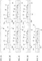
Figures 1A to 1E are exemplary of possible acts in embodiments, -
Figures 2A to 2E are exemplary of possible acts in embodiments, -
Figures 3A and 3B are exemplary of possible variants in embodiments, and -
Figures 4A and 4B are exemplary of possible variants in embodiments. - In the ensuing description, one or more specific details are illustrated, aimed at providing an in-depth understanding of examples of embodiments of this description. The embodiments may be obtained without one or more of the specific details, or with other methods, components, materials, etc. In other cases, known structures, materials, or operations are not illustrated or described in detail so that certain aspects of embodiments will not be obscured.
- Reference to "an embodiment" or "one embodiment" in the framework of the present description is intended to indicate that a particular configuration, structure, or characteristic described in relation to the embodiment is comprised in at least one embodiment. Hence, phrases such as "in an embodiment" or "in one embodiment" that may be present in one or more points of the present description do not necessarily refer to one and the same embodiment. Moreover, particular conformations, structures, or characteristics may be combined in any adequate way in one or more embodiments.
- The references used herein are provided merely for convenience and hence do not define the extent of protection or the scope of the embodiments.
- One or more embodiments as exemplified herein facilitate providing a full-mold package for an electronic device suited to be produced by resorting to standard and generally available technologies while pursuing a reduction of the total thickness of the resulting device.
- One or more embodiments may be applied, for instance, to
electronics devices 10 comprising: - at least one first
electronic component 12 such as a sensor (a MEMS sensor being exemplary of such an component), and - at least one second
electronic component 14 such as associated "companion" semiconductor chip or die (an ASIC being exemplary of such a semiconductor chip or die) mounted on arespective substrate 16. - The designation "respective" highlights the fact that, in one or more embodiments as exemplified herein, the substrate 16 (which may be regarded as akin to a printed circuit board or PCB) is intended to support (only) the
semiconductor chip 14 and not thesensor component 12, so that the thickness of thesubstrate 16 does not add to the thickness of thesensor 12. - As exemplified herein, the
first component 12 will exhibit a front or "top"surface 12a and a rear or "bottom"surface 12b with a thickness of thecomponent 12 identified by the distance between thesurfaces - As discussed previously, an object pursued by embodiments is to reduce the total thickness of the
device 10 by letting such a thickness be essentially determined by the thickness of the component 12 (a sensor such as a MEMS, for instance), possibly with both surfaces or sides of the component 12 (namely thefront surface 12a and theback surface 12b) exposed at the package surface. - In one or more embodiments as portrayed in a first exemplary sequence of acts in
Figures 1A to 1E , a (sacrificial)carrier 20 is provided (Figure 1A ) onto which the component 12 (e.g. a sensor) and a companion component 14 (e.g. a semiconductor chip) are arranged side-by-side with thecomponent 14 mounted on thesubstrate 16. This may be viabumps 18, as conventional in the art. -
Figures 1B to 1D are exemplary of acts in a manufacturing process which can be performed on a plurality of similar structures or assemblies arranged on a tape-like carrier 20, with these structures eventually separated in a "singulation" step as exemplified inFigure 1D to provide individual devices 10 (Figure IE). - In one or more embodiments, the
carrier 20 may include a tape (a polycarbonate tape, for instance) as conventional in manufacturing processes of integrated circuits (ICs). - Once the
components 12 and 14 (this latter mounted on the substrate 16) are arranged side-by-side on thecarrier 20, withelectrical coupling 22 provided therebetween as desired (again by conventional solutions, such as wire bonding, for instance) apackage molding compound 24 can be molded onto the previously formed assembly as exemplified inFigure 1C , that is by leaving exposed the "cap", namely thefront surface 12a of thecomponent 12. - An Epoxy Molding Compound (EMC) may be exemplary of a compound as 24.
-
Figure 1D is exemplary of a singulation act (performed, in conventional manner, via a singulation tool indicated S) followed by removal of the carrier 20 (Figure IE) leading to both the front side orsurface 12a and the rear orback side 12b of thecomponent 12 being exposed at the surface of themolding material 24. - As a result the package thickness of the
device 10 is determined by (that is, essentially the same as) the thickness of thecomponent 12 alone (that is the thickness between thesurfaces - Also, while the
opposed surfaces component 12 are exposed at the package surface, the material of the component 14 (a semiconductor such as silicon, for instance) is embedded and thus "floating" within thepackage molding compound 24. - Those of skill in the art will easily appreciate that the sequence of acts of
Figures 1A to 1E is merely exemplary and non-mandatory: for instance, singulation, here exemplified before removal of thecarrier 20, may take place after or simultaneously with removal of thecarrier 20. - In
Figures 2A to 2E parts, components or acts like parts, components or acts already discussed in connection withFigures 1A to 1E are indicated with like reference symbols. A corresponding detailed description will not be repeated for brevity. - In embodiments as exemplified in
Figures 2A to 2E electrical coupling of the component (semiconductor chip) 14 to thesubstrate 16 is achieved via wire-bonding (again indicated 22) in the place of bumps such asbumps 18 inFigures 1B to 1E . - Here again, the package thickness of the
device 10 is essentially determined by the thickness of thecomponent 12 alone (that is the thickness between thesurfaces wire bond loops 22 having no practical impact on the total thickness of thedevice 10 even taking into account the thickness of thecomponent 14 and the substrate (which may be reasonably expected to be thinner than the component 12). - Here again, while the
opposed surfaces component 12 are exposed at the package surface, the material of the component 14 (a semiconductor such as silicon, for instance) is embedded and thus "floating" within thepackage molding compound 24. -
Figures 3A and 3B can be regarded as essentially corresponding toFigures 1D and 1E with parts, components or acts already discussed in connection withFigures 1A to 1E indicated with like reference symbols. A corresponding detailed description will not be repeated for brevity. -
Figures 3A and 3B are exemplary of the possibility (which may apply both to embodiments as exemplified inFigures 1A to 1E and to embodiments as exemplified inFigures 2A to 2E ) of providingelectromagnetic shielding material 26 onto the top or front surface of the component 10 (including the front ortop surface 12a of the component 12). - Such an approach may be advantageous in case the component 12 (a sensor component, for instance) is sensitive to electromagnetic signal.
- The
shielding material 26 may comprise (in a manner known to those of skill in the art) electrically-conductive material such as a metal which can be applied onto thecomponent 10 after device singulation and possible dedicated substrate design. -
Figures 4A and 4B can be regarded again as essentially corresponding toFigures 1D and 1E with parts, components or acts already discussed in connection withFigures 1A to 1E indicated with like reference symbols. A corresponding detailed description will not be repeated for brevity. -
Figure 4A and 4B are exemplary of the possibility (which may apply both to embodiments as exemplified inFigures 1A to 1E and to embodiments as exemplified inFigures 2A to 2E ) of providing a (very) thin sensor - a differential pressure sensor, for instance - withpressure ports 120 provided at the exposed surfaces (for instance both thefront surface 12a and theback surface 12b) of thesensor component 12. - Also those of skill in the art will appreciated that the stepped outline of the sides of the device in
Figures 4A and 4B is indicative of the possibility, in one or more embodiments, of providingshielding 26 as exemplified inFigures 3A and 3B also in arrangements as exemplified inFigures 4A and 4B . - One or more embodiments thus make it possible to reduce the thickness of the
device 10 by letting it be essentially given by the thickness of the first component 12 (a MEMS, for instance) without any contribution to the device thickness given by thesubstrate 16 for thecompanion component 14 and/or by the mold chase thickness. - In one or more embodiments as exemplified herein the (total) thickness of the molded package (see
Figures 1E ,2E ,3B and 4B , for instance) is determined by the thickness of a single component (here, the component 12) which, contrary to thecomponent 14, has no associated substrate by avoiding a combination with the substrate and/or mold material thickness. - Also, one or more embodiments lend themselves (in the case of a small routing specifications and/or low signal count, for instance) to implementations where the substrate (16 in the figures) is provided via a copper frame.
- Also, certain embodiments (this may be the case of non-capped devices) may facilitate using a
component 14 provided with a "dummy" die/interposer mounted on top. This may be advantageous in cases where the exposed front and/or back sides of the component may facilitate (via such a dummy die for instance) a thermal dissipation function and/or a thermal sensing function. - In one or more embodiments, electromagnetic interference (EMI) shielding can be enhanced by resorting to a shielding (metalized, for instance) backside and/or to conductive dummy dies at one or both of the opposed surfaces.
- A method as exemplified herein may comprise:
- providing a (planar, for instance) support member (for instance, 20),
- arranging on the support member:
- a) at least one first electronic component (for instance, 12) having opposed first (for instance, 12a) and second (for instance, 12b) surfaces, the at least one first electronic component arranged on the support member with the second surface towards the support member, wherein the at least one first electronic component has a thickness between the opposed first and second surfaces (for instance, between 12a and 12b),
- b) at least one second electronic component (for instance, 14) mounted on a substrate (for instance, 16), the at least one second electronic component arranged on the support member with the substrate having a substrate surface (facing downwards, in the figures) opposed the at least one second electronic component and facing towards the support member, wherein the substrate and the at least one second electronic component mounted thereon have a joint (that is, cumulative) thickness which is less than the thickness of the at least one first electronic component (see, for instance
Figures 1B thru 1E ,Figures 2B thru 2E ,3A and 3B, 4A and 4B ), - molding package molding material (for instance, 24) onto the support member having arranged thereon the at least one first electronic component and the at least one second electronic component mounted on the substrate, wherein the package molding material encapsulates the at least one second electronic component leaving exposed (at the surface of the molding material) the first surface of the at least one first electronic component (see, for instance,
Figures 1C ,2C ,3A and 4A ), and - separating (removing, for instance) the support member to expose the second surface of the at least one first electronic component and the substrate surface of the substrate opposed the at least one second electronic component (see, for instance,
Figures 1E ,2E ,3B and 4B ). - A method as exemplified herein may comprise:
- a) providing electrically-conductive formations (for instance, 18 or 22) between:
- the at least one second electronic component and the substrate (see, for instance, the
bumps 18 inFigures 1B to 1E or thewires 22 on the right side of thecomponent 14 inFigures 2B to 2E ), and/or - the at least one first electronic component and the substrate (see, for instance, the
wires 22 on the right side of thecomponent 12 inFigures 1B to 1E and 2B to 2E), and/or - the at least one first electronic component and the at least one second electronic component (see, for instance, the
wires 22 between thecomponents Figures 2B to 2E ), - b) molding the package molding material onto the support member having arranged thereon the at least one first electronic component and the at least one second electronic component mounted on the substrate, wherein the package molding material encapsulates said electrically-conductive formations.
- A method as exemplified herein may comprise providing electromagnetic shielding material (for instance, 26) over at least one (for instance, 12a) of the first and second opposed surfaces of the at least one first electronic component. As discussed a "dummy" shield may be provided on either of both of these surfaces.
- In a method as exemplified herein the at least one first electronic component may comprise a pressure sensor with at least one of the opposed first and second surfaces provided with pressure ports (for instance, 120).
- In a method as exemplified herein, the support member may comprises a tape.
- In a method as exemplified herein:
- the at least one first electronic component may comprise a sensor, optionally a MEMS, and/or
- the at least one second electronic component may comprise a semiconductor chip, optionally an ASIC.
- A method as exemplified herein may comprise:
- arranging on the support member a sequence of assemblies, wherein each assembly may comprise:
- a) at least one first electronic component having opposed first and second surfaces, the at least one first electronic component arranged on the support member with the second surface towards the support member, wherein the at least one first electronic component has a thickness between the opposed first and second surfaces,
- b) at least one second electronic component mounted on a substrate, the at least one second electronic component arranged on the support member with the substrate having a substrate surface opposed the at least one second electronic component and facing towards the support member, wherein the substrate and the at least one second electronic component mounted thereon have a joint thickness with is less than the thickness of the at least one first electronic component,
- molding onto the support member having arranged thereon said sequence of assemblies, package molding material to encapsulate the at least one second electronic component in the assemblies in said sequence of assemblies leaving exposed the first surface of the at least one electronic component in the assemblies in said sequence of assemblies,
- separating the support member to expose the second surface of the at least one first electronic component and the substrate surface of the substrate opposed the at least one second electronic component in the assemblies in said sequence of assemblies, and
- singulating (for instance, S) said sequence of assemblies into individual devices including at least one said first electronic component and least one said second electronic component coupled therewith.
- A device (for instance, 10) as exemplified herein, may comprise:
- at least one first electronic component having opposed first and second surfaces, the at least one first electronic component arranged on the support member with the second surface towards the support member, wherein the at least one first electronic component has a thickness between the opposed first and second surfaces,
- at least one second electronic component mounted on a substrate, the at least one second electronic component arranged on the support member with the substrate having a substrate surface opposed the at least one second electronic component and facing towards the support member, wherein the substrate and the at least one second electronic component mounted thereon have a joint thickness with is less than the thickness of the at least one first electronic component, and
- package molding material encapsulating the at least one second electronic component leaving exposed the opposed first and second surfaces of the at least one electronic component and the substrate surface of the substrate opposed the at least one second electronic component.
- A device as exemplified herein may comprise electrically-conductive formations between:
- the at least one second electronic component and the substrate, and/or
- the at least one first electronic component and the substrate, and/or
- the at least one first electronic component and the at least one second electronic component,
- A device as exemplified herein may comprise electromagnetic shielding material over at least one of the first and second opposed surfaces of the at least one first electronic component.
- In a device as exemplified herein the at least one first electronic component may comprise a pressure sensor, with at least one of the opposed first and second surfaces provided with pressure ports.
- In a device as exemplified herein:
- the at least one first electronic component (12) may comprise a sensor, optionally a MEMS, and/or
- the at least one second electronic component (14) may comprise a semiconductor chip, optionally an ASIC.
- Without prejudice to the underlying principles, the details and embodiments may vary, even significantly, with respect to what has been described by way of example only, without departing from the scope of protection.
- The extent of protection is determined by the annexed claims.
Claims (12)
- A method, comprising:- providing a support member (20),- arranging on the support member:- a) at least one first electronic component (12) having opposed first (12a) and second (12b) surfaces, the at least one first electronic component (12) arranged on the support member (20) with the second surface (12b) towards the support member (20), wherein the at least one first electronic component (12) has a thickness between the opposed first (12a) and second (12b) surfaces,- b) at least one second electronic component (14) mounted on a substrate (16), the at least one second electronic component (14) arranged on the support member (20) with the substrate (16) having a substrate surface opposed the at least one second electronic component (14) and facing towards the support member (20), wherein the substrate (16) and the at least one second electronic component (14) mounted thereon have a joint thickness which is less than the thickness of the at least one first electronic component (12),- molding package molding material (24) onto the support member (20) having arranged thereon the at least one first electronic component (12) and the at least one second electronic component (14) mounted on the substrate (16), wherein the package molding material (24) encapsulates the at least one second electronic component (14) leaving exposed the first surface (12a) of the at least one first electronic component (12), and- separating the support member (20) to expose the second surface (12b) of the at least one first electronic component (12) and the substrate surface of the substrate (16) opposed the at least one second electronic component (14).
- The method of claim 1, comprising:- a) providing electrically-conductive formations (18, 22; 22) between:- the at least one second electronic component (12) and the substrate (16), and/or- the at least one first electronic component (12) and the substrate (16), and/or- the at least one first electronic component (12) and the at least one second electronic component (14),- b) molding the package molding material (24) onto the support member (20) having arranged thereon the at least one first electronic component (12) and the at least one second electronic component (14) mounted on the substrate (16), wherein the package molding material (24) encapsulates said electrically-conductive formations (18, 22; 22).
- The method of claim 1 or claim 2, comprising providing electromagnetic shielding material (26) over at least one (12a) of the first (12a) and second (12b) opposed surfaces of the at least one first electronic component (12).
- The method of any of the previous claims, wherein the at least one first electronic component (12) comprises a pressure sensor with at least one of the opposed first (12a) and second (12b) surfaces provided with pressure ports (120).
- The method of any of the previous claims, wherein the support member (20) comprises a tape.
- The method of any of the previous claims, wherein:- the at least one first electronic component (12) comprises a sensor, preferably a MEMS, and/or- the at least one second electronic component (14) comprises a semiconductor chip (14), preferably an ASIC.
- The method of any of the previous claims, comprising:- arranging on the support member (20) a sequence of assemblies, each assembly comprising:- a) at least one first electronic component (12) having opposed first (12a) and second (12b) surfaces, the at least one first electronic component (12) arranged on the support member (20) with the second surface (12b) towards the support member (20), wherein the at least one first electronic component (12) has a thickness between the opposed first (12a) and second (12b) surfaces,- b) at least one second electronic component (14) mounted on a substrate (16), the at least one second electronic component (14) arranged on the support member (20) with the substrate (16) having a substrate surface opposed the at least one second electronic component (14) and facing towards the support member (20), wherein the substrate (16) and the at least one second electronic component (14) mounted thereon have a joint thickness with is less than the thickness of the at least one first electronic component (12),- molding onto the support member (20) having arranged thereon said sequence of assemblies, package molding material (24) to encapsulate the at least one second electronic component (14) in the assemblies in said sequence of assemblies leaving exposed the first surface (12a) of the at least one electronic component (12) in the assemblies in said sequence of assemblies,- separating the support member (20) to expose the second surface (12b) of the at least one first electronic component (12) and the substrate surface of the substrate (16) opposed the at least one second electronic component (14) in the assemblies in said sequence of assemblies, and- singulating (S) said sequence of assemblies into individual devices (10) including at least one said first electronic component (12) and least one said second electronic component (14) coupled therewith.
- A device (10), comprising:- at least one first electronic component (12) having opposed first (12a) and second (12b) surfaces, the at least one first electronic component (12) arranged on a support member (20) with the second surface (12b) towards the support member (20), wherein the at least one first electronic component (12) has a thickness between the opposed first (12a) and second (12b) surfaces,- at least one second electronic component (14) mounted on a substrate (16), the at least one second electronic component (14) arranged on the support member (20) with the substrate (16) having a substrate surface opposed the at least one second electronic component (14) and facing towards the support member (20), wherein the substrate (16) and the at least one second electronic component (14) mounted thereon have a joint thickness which is less than the thickness of the at least one first electronic component (12), and- package molding material (24) encapsulating the at least one second electronic component (14), said package molding material (24) leaving exposed the opposed first (12a) and second (12b) surfaces of the at least one electronic component (12) and the substrate surface of the substrate (16) opposed the at least one second electronic component (14).
- The device (10) of claim 8, comprising electrically-conductive formations (18, 22; 22) between:- the at least one second electronic component (12) and the substrate (16), and/or- the at least one first electronic component (12) and the substrate (16), and/or- the at least one first electronic component (12) and the at least one second electronic component (14), wherein said package molding material (24) encapsulates said electrically-conductive formations (18, 22; 22).
- The device (10) of claim 8 or claim 9, comprising electromagnetic shielding material (26) over at least one (12a) of the first (12a) and second (12b) opposed surfaces of the at least one first electronic component (12).
- The device (10) of any of claims 8 to 10, wherein the at least one first electronic component (12) comprises a pressure sensor, with at least one of the opposed first (12a) and second (12b) surfaces provided with pressure ports (120).
- The device (10) of any of claims 8 to 11, wherein:- the at least one first electronic component (12) comprises a sensor, preferably a MEMS, and/or- the at least one second electronic component (14) comprises a semiconductor chip (14), preferably an ASIC.
Applications Claiming Priority (1)
| Application Number | Priority Date | Filing Date | Title |
|---|---|---|---|
| IT102019000004835A IT201900004835A1 (en) | 2019-04-01 | 2019-04-01 | PROCEDURE FOR PRODUCING ELECTRONIC DEVICES AND CORRESPONDING ELECTRONIC DEVICE |
Publications (2)
| Publication Number | Publication Date |
|---|---|
| EP3718961A1 true EP3718961A1 (en) | 2020-10-07 |
| EP3718961B1 EP3718961B1 (en) | 2024-07-10 |
Family
ID=66867709
Family Applications (1)
| Application Number | Title | Priority Date | Filing Date |
|---|---|---|---|
| EP20164126.3A Active EP3718961B1 (en) | 2019-04-01 | 2020-03-19 | A method of manufacturing electronic devices and corresponding electronic device |
Country Status (4)
| Country | Link |
|---|---|
| US (2) | US11524892B2 (en) |
| EP (1) | EP3718961B1 (en) |
| CN (2) | CN111792620A (en) |
| IT (1) | IT201900004835A1 (en) |
Families Citing this family (1)
| Publication number | Priority date | Publication date | Assignee | Title |
|---|---|---|---|---|
| IT201900004835A1 (en) * | 2019-04-01 | 2020-10-01 | Stmicroelectronics Malta Ltd | PROCEDURE FOR PRODUCING ELECTRONIC DEVICES AND CORRESPONDING ELECTRONIC DEVICE |
Citations (2)
| Publication number | Priority date | Publication date | Assignee | Title |
|---|---|---|---|---|
| DE102014115509A1 (en) * | 2013-10-25 | 2015-04-30 | Infineon Technologies Ag | Semiconductor component and method for manufacturing a semiconductor device |
| DE102015108335A1 (en) * | 2014-05-27 | 2015-12-03 | Infineon Technologies Ag | LADDER-FRAME-BASED MEMS SENSOR STRUCTURE |
Family Cites Families (9)
| Publication number | Priority date | Publication date | Assignee | Title |
|---|---|---|---|---|
| US20090057885A1 (en) * | 2007-08-30 | 2009-03-05 | Infineon Technologies Ag | Semiconductor device |
| US8084300B1 (en) * | 2010-11-24 | 2011-12-27 | Unisem (Mauritius) Holdings Limited | RF shielding for a singulated laminate semiconductor device package |
| US20130075892A1 (en) * | 2011-09-27 | 2013-03-28 | Taiwan Semiconductor Manufacturing Company, Ltd. | Method for Three Dimensional Integrated Circuit Fabrication |
| US9006896B2 (en) * | 2012-05-07 | 2015-04-14 | Xintec Inc. | Chip package and method for forming the same |
| US9663357B2 (en) * | 2015-07-15 | 2017-05-30 | Texas Instruments Incorporated | Open cavity package using chip-embedding technology |
| US10535611B2 (en) * | 2015-11-20 | 2020-01-14 | Apple Inc. | Substrate-less integrated components |
| US9704812B1 (en) * | 2016-05-06 | 2017-07-11 | Atmel Corporation | Double-sided electronic package |
| CN111217318B (en) * | 2018-11-26 | 2024-12-27 | 罗伯特·博世有限公司 | Sensors and packaging components |
| IT201900004835A1 (en) * | 2019-04-01 | 2020-10-01 | Stmicroelectronics Malta Ltd | PROCEDURE FOR PRODUCING ELECTRONIC DEVICES AND CORRESPONDING ELECTRONIC DEVICE |
-
2019
- 2019-04-01 IT IT102019000004835A patent/IT201900004835A1/en unknown
-
2020
- 2020-03-19 EP EP20164126.3A patent/EP3718961B1/en active Active
- 2020-03-30 US US16/834,042 patent/US11524892B2/en active Active
- 2020-03-31 CN CN202010245402.3A patent/CN111792620A/en active Pending
- 2020-03-31 CN CN202020446628.5U patent/CN212387732U/en active Active
-
2022
- 2022-12-12 US US18/079,704 patent/US12017910B2/en active Active
Patent Citations (2)
| Publication number | Priority date | Publication date | Assignee | Title |
|---|---|---|---|---|
| DE102014115509A1 (en) * | 2013-10-25 | 2015-04-30 | Infineon Technologies Ag | Semiconductor component and method for manufacturing a semiconductor device |
| DE102015108335A1 (en) * | 2014-05-27 | 2015-12-03 | Infineon Technologies Ag | LADDER-FRAME-BASED MEMS SENSOR STRUCTURE |
Also Published As
| Publication number | Publication date |
|---|---|
| IT201900004835A1 (en) | 2020-10-01 |
| CN111792620A (en) | 2020-10-20 |
| US11524892B2 (en) | 2022-12-13 |
| CN212387732U (en) | 2021-01-22 |
| US20230110259A1 (en) | 2023-04-13 |
| EP3718961B1 (en) | 2024-07-10 |
| US20200307994A1 (en) | 2020-10-01 |
| US12017910B2 (en) | 2024-06-25 |
Similar Documents
| Publication | Publication Date | Title |
|---|---|---|
| US7030469B2 (en) | Method of forming a semiconductor package and structure thereof | |
| US11127645B2 (en) | Grounding lids in integrated circuit devices | |
| CN107240583B (en) | Multichip Pressure Sensor Package | |
| US8653634B2 (en) | EMI-shielded semiconductor devices and methods of making | |
| KR20090060132A (en) | Electromagnetically Isolated Integrated Circuit Package System | |
| EP3138126B1 (en) | Electronic assembly comprising a carrier structure made from a printed circuit board | |
| WO2006036548A2 (en) | Method of forming a semiconductor package and structure thereof | |
| US10211184B2 (en) | Apparatus and methods for multi-die packaging | |
| US20180122731A1 (en) | Plated ditch pre-mold lead frame, semiconductor package, and method of making same | |
| US20170084519A1 (en) | Semiconductor package and method of manufacturing same | |
| CN107265393B (en) | Semiconductor device including MEMS die | |
| KR20140081859A (en) | Wafer level applied rf shields | |
| EP1946369B1 (en) | Method of packaging semiconductor dies | |
| SG173394A1 (en) | Integrated circuit leadframe and fabrication method therefor | |
| US7633763B1 (en) | Double mold memory card and its manufacturing method | |
| US12017910B2 (en) | Method of manufacturing electronic devices and corresponding electronic device | |
| US20150160087A1 (en) | Stacked die sensor package | |
| US7723163B2 (en) | Method of forming premolded lead frame | |
| US8193620B2 (en) | Integrated circuit package with enlarged die paddle | |
| US5963782A (en) | Semiconductor component and method of manufacture | |
| US20170033058A1 (en) | Structures and methods for semiconductor packaging | |
| US9034697B2 (en) | Apparatus and methods for quad flat no lead packaging | |
| KR20130046068A (en) | Manufacturing method of semiconductor package and semiconductor package using the same | |
| US20140220738A1 (en) | Lead frame array package with flip chip die attach | |
| CN116646311A (en) | electronic device |
Legal Events
| Date | Code | Title | Description |
|---|---|---|---|
| PUAI | Public reference made under article 153(3) epc to a published international application that has entered the european phase |
Free format text: ORIGINAL CODE: 0009012 |
|
| STAA | Information on the status of an ep patent application or granted ep patent |
Free format text: STATUS: THE APPLICATION HAS BEEN PUBLISHED |
|
| AK | Designated contracting states |
Kind code of ref document: A1 Designated state(s): AL AT BE BG CH CY CZ DE DK EE ES FI FR GB GR HR HU IE IS IT LI LT LU LV MC MK MT NL NO PL PT RO RS SE SI SK SM TR |
|
| AX | Request for extension of the european patent |
Extension state: BA ME |
|
| STAA | Information on the status of an ep patent application or granted ep patent |
Free format text: STATUS: REQUEST FOR EXAMINATION WAS MADE |
|
| 17P | Request for examination filed |
Effective date: 20210201 |
|
| RBV | Designated contracting states (corrected) |
Designated state(s): AL AT BE BG CH CY CZ DE DK EE ES FI FR GB GR HR HU IE IS IT LI LT LU LV MC MK MT NL NO PL PT RO RS SE SI SK SM TR |
|
| STAA | Information on the status of an ep patent application or granted ep patent |
Free format text: STATUS: EXAMINATION IS IN PROGRESS |
|
| 17Q | First examination report despatched |
Effective date: 20220712 |
|
| GRAP | Despatch of communication of intention to grant a patent |
Free format text: ORIGINAL CODE: EPIDOSNIGR1 |
|
| STAA | Information on the status of an ep patent application or granted ep patent |
Free format text: STATUS: GRANT OF PATENT IS INTENDED |
|
| INTG | Intention to grant announced |
Effective date: 20240315 |
|
| GRAS | Grant fee paid |
Free format text: ORIGINAL CODE: EPIDOSNIGR3 |
|
| GRAA | (expected) grant |
Free format text: ORIGINAL CODE: 0009210 |
|
| STAA | Information on the status of an ep patent application or granted ep patent |
Free format text: STATUS: THE PATENT HAS BEEN GRANTED |
|
| AK | Designated contracting states |
Kind code of ref document: B1 Designated state(s): AL AT BE BG CH CY CZ DE DK EE ES FI FR GB GR HR HU IE IS IT LI LT LU LV MC MK MT NL NO PL PT RO RS SE SI SK SM TR |
|
| REG | Reference to a national code |
Ref country code: CH Ref legal event code: EP |
|
| REG | Reference to a national code |
Ref country code: DE Ref legal event code: R096 Ref document number: 602020033608 Country of ref document: DE |
|
| REG | Reference to a national code |
Ref country code: LT Ref legal event code: MG9D |
|
| REG | Reference to a national code |
Ref country code: NL Ref legal event code: MP Effective date: 20240710 |
|
| PG25 | Lapsed in a contracting state [announced via postgrant information from national office to epo] |
Ref country code: PT Free format text: LAPSE BECAUSE OF FAILURE TO SUBMIT A TRANSLATION OF THE DESCRIPTION OR TO PAY THE FEE WITHIN THE PRESCRIBED TIME-LIMIT Effective date: 20241111 |
|
| REG | Reference to a national code |
Ref country code: AT Ref legal event code: MK05 Ref document number: 1701932 Country of ref document: AT Kind code of ref document: T Effective date: 20240710 |
|
| PG25 | Lapsed in a contracting state [announced via postgrant information from national office to epo] |
Ref country code: NL Free format text: LAPSE BECAUSE OF FAILURE TO SUBMIT A TRANSLATION OF THE DESCRIPTION OR TO PAY THE FEE WITHIN THE PRESCRIBED TIME-LIMIT Effective date: 20240710 |
|
| PG25 | Lapsed in a contracting state [announced via postgrant information from national office to epo] |
Ref country code: PT Free format text: LAPSE BECAUSE OF FAILURE TO SUBMIT A TRANSLATION OF THE DESCRIPTION OR TO PAY THE FEE WITHIN THE PRESCRIBED TIME-LIMIT Effective date: 20241111 Ref country code: NL Free format text: LAPSE BECAUSE OF FAILURE TO SUBMIT A TRANSLATION OF THE DESCRIPTION OR TO PAY THE FEE WITHIN THE PRESCRIBED TIME-LIMIT Effective date: 20240710 |
|
| PG25 | Lapsed in a contracting state [announced via postgrant information from national office to epo] |
Ref country code: NO Free format text: LAPSE BECAUSE OF FAILURE TO SUBMIT A TRANSLATION OF THE DESCRIPTION OR TO PAY THE FEE WITHIN THE PRESCRIBED TIME-LIMIT Effective date: 20241010 |
|
| PG25 | Lapsed in a contracting state [announced via postgrant information from national office to epo] |
Ref country code: PL Free format text: LAPSE BECAUSE OF FAILURE TO SUBMIT A TRANSLATION OF THE DESCRIPTION OR TO PAY THE FEE WITHIN THE PRESCRIBED TIME-LIMIT Effective date: 20240710 Ref country code: FI Free format text: LAPSE BECAUSE OF FAILURE TO SUBMIT A TRANSLATION OF THE DESCRIPTION OR TO PAY THE FEE WITHIN THE PRESCRIBED TIME-LIMIT Effective date: 20240710 Ref country code: GR Free format text: LAPSE BECAUSE OF FAILURE TO SUBMIT A TRANSLATION OF THE DESCRIPTION OR TO PAY THE FEE WITHIN THE PRESCRIBED TIME-LIMIT Effective date: 20241011 |
|
| PG25 | Lapsed in a contracting state [announced via postgrant information from national office to epo] |
Ref country code: BG Free format text: LAPSE BECAUSE OF FAILURE TO SUBMIT A TRANSLATION OF THE DESCRIPTION OR TO PAY THE FEE WITHIN THE PRESCRIBED TIME-LIMIT Effective date: 20240710 |
|
| PG25 | Lapsed in a contracting state [announced via postgrant information from national office to epo] |
Ref country code: LV Free format text: LAPSE BECAUSE OF FAILURE TO SUBMIT A TRANSLATION OF THE DESCRIPTION OR TO PAY THE FEE WITHIN THE PRESCRIBED TIME-LIMIT Effective date: 20240710 |
|
| PG25 | Lapsed in a contracting state [announced via postgrant information from national office to epo] |
Ref country code: AT Free format text: LAPSE BECAUSE OF FAILURE TO SUBMIT A TRANSLATION OF THE DESCRIPTION OR TO PAY THE FEE WITHIN THE PRESCRIBED TIME-LIMIT Effective date: 20240710 Ref country code: IS Free format text: LAPSE BECAUSE OF FAILURE TO SUBMIT A TRANSLATION OF THE DESCRIPTION OR TO PAY THE FEE WITHIN THE PRESCRIBED TIME-LIMIT Effective date: 20241110 |
|
| PG25 | Lapsed in a contracting state [announced via postgrant information from national office to epo] |
Ref country code: HR Free format text: LAPSE BECAUSE OF FAILURE TO SUBMIT A TRANSLATION OF THE DESCRIPTION OR TO PAY THE FEE WITHIN THE PRESCRIBED TIME-LIMIT Effective date: 20240710 |
|
| PG25 | Lapsed in a contracting state [announced via postgrant information from national office to epo] |
Ref country code: RS Free format text: LAPSE BECAUSE OF FAILURE TO SUBMIT A TRANSLATION OF THE DESCRIPTION OR TO PAY THE FEE WITHIN THE PRESCRIBED TIME-LIMIT Effective date: 20241010 Ref country code: ES Free format text: LAPSE BECAUSE OF FAILURE TO SUBMIT A TRANSLATION OF THE DESCRIPTION OR TO PAY THE FEE WITHIN THE PRESCRIBED TIME-LIMIT Effective date: 20240710 |
|
| PG25 | Lapsed in a contracting state [announced via postgrant information from national office to epo] |
Ref country code: RS Free format text: LAPSE BECAUSE OF FAILURE TO SUBMIT A TRANSLATION OF THE DESCRIPTION OR TO PAY THE FEE WITHIN THE PRESCRIBED TIME-LIMIT Effective date: 20241010 Ref country code: PL Free format text: LAPSE BECAUSE OF FAILURE TO SUBMIT A TRANSLATION OF THE DESCRIPTION OR TO PAY THE FEE WITHIN THE PRESCRIBED TIME-LIMIT Effective date: 20240710 Ref country code: NO Free format text: LAPSE BECAUSE OF FAILURE TO SUBMIT A TRANSLATION OF THE DESCRIPTION OR TO PAY THE FEE WITHIN THE PRESCRIBED TIME-LIMIT Effective date: 20241010 Ref country code: LV Free format text: LAPSE BECAUSE OF FAILURE TO SUBMIT A TRANSLATION OF THE DESCRIPTION OR TO PAY THE FEE WITHIN THE PRESCRIBED TIME-LIMIT Effective date: 20240710 Ref country code: IS Free format text: LAPSE BECAUSE OF FAILURE TO SUBMIT A TRANSLATION OF THE DESCRIPTION OR TO PAY THE FEE WITHIN THE PRESCRIBED TIME-LIMIT Effective date: 20241110 Ref country code: HR Free format text: LAPSE BECAUSE OF FAILURE TO SUBMIT A TRANSLATION OF THE DESCRIPTION OR TO PAY THE FEE WITHIN THE PRESCRIBED TIME-LIMIT Effective date: 20240710 Ref country code: GR Free format text: LAPSE BECAUSE OF FAILURE TO SUBMIT A TRANSLATION OF THE DESCRIPTION OR TO PAY THE FEE WITHIN THE PRESCRIBED TIME-LIMIT Effective date: 20241011 Ref country code: FI Free format text: LAPSE BECAUSE OF FAILURE TO SUBMIT A TRANSLATION OF THE DESCRIPTION OR TO PAY THE FEE WITHIN THE PRESCRIBED TIME-LIMIT Effective date: 20240710 Ref country code: ES Free format text: LAPSE BECAUSE OF FAILURE TO SUBMIT A TRANSLATION OF THE DESCRIPTION OR TO PAY THE FEE WITHIN THE PRESCRIBED TIME-LIMIT Effective date: 20240710 Ref country code: BG Free format text: LAPSE BECAUSE OF FAILURE TO SUBMIT A TRANSLATION OF THE DESCRIPTION OR TO PAY THE FEE WITHIN THE PRESCRIBED TIME-LIMIT Effective date: 20240710 Ref country code: AT Free format text: LAPSE BECAUSE OF FAILURE TO SUBMIT A TRANSLATION OF THE DESCRIPTION OR TO PAY THE FEE WITHIN THE PRESCRIBED TIME-LIMIT Effective date: 20240710 |
|
| REG | Reference to a national code |
Ref country code: DE Ref legal event code: R097 Ref document number: 602020033608 Country of ref document: DE |
|
| PG25 | Lapsed in a contracting state [announced via postgrant information from national office to epo] |
Ref country code: DK Free format text: LAPSE BECAUSE OF FAILURE TO SUBMIT A TRANSLATION OF THE DESCRIPTION OR TO PAY THE FEE WITHIN THE PRESCRIBED TIME-LIMIT Effective date: 20240710 Ref country code: SM Free format text: LAPSE BECAUSE OF FAILURE TO SUBMIT A TRANSLATION OF THE DESCRIPTION OR TO PAY THE FEE WITHIN THE PRESCRIBED TIME-LIMIT Effective date: 20240710 Ref country code: RO Free format text: LAPSE BECAUSE OF FAILURE TO SUBMIT A TRANSLATION OF THE DESCRIPTION OR TO PAY THE FEE WITHIN THE PRESCRIBED TIME-LIMIT Effective date: 20240710 |
|
| PG25 | Lapsed in a contracting state [announced via postgrant information from national office to epo] |
Ref country code: EE Free format text: LAPSE BECAUSE OF FAILURE TO SUBMIT A TRANSLATION OF THE DESCRIPTION OR TO PAY THE FEE WITHIN THE PRESCRIBED TIME-LIMIT Effective date: 20240710 |
|
| PG25 | Lapsed in a contracting state [announced via postgrant information from national office to epo] |
Ref country code: CZ Free format text: LAPSE BECAUSE OF FAILURE TO SUBMIT A TRANSLATION OF THE DESCRIPTION OR TO PAY THE FEE WITHIN THE PRESCRIBED TIME-LIMIT Effective date: 20240710 |
|
| PG25 | Lapsed in a contracting state [announced via postgrant information from national office to epo] |
Ref country code: IT Free format text: LAPSE BECAUSE OF FAILURE TO SUBMIT A TRANSLATION OF THE DESCRIPTION OR TO PAY THE FEE WITHIN THE PRESCRIBED TIME-LIMIT Effective date: 20240710 Ref country code: SK Free format text: LAPSE BECAUSE OF FAILURE TO SUBMIT A TRANSLATION OF THE DESCRIPTION OR TO PAY THE FEE WITHIN THE PRESCRIBED TIME-LIMIT Effective date: 20240710 |
|
| PLBE | No opposition filed within time limit |
Free format text: ORIGINAL CODE: 0009261 |
|
| STAA | Information on the status of an ep patent application or granted ep patent |
Free format text: STATUS: NO OPPOSITION FILED WITHIN TIME LIMIT |
|
| 26N | No opposition filed |
Effective date: 20250411 |
|
| PG25 | Lapsed in a contracting state [announced via postgrant information from national office to epo] |
Ref country code: SE Free format text: LAPSE BECAUSE OF FAILURE TO SUBMIT A TRANSLATION OF THE DESCRIPTION OR TO PAY THE FEE WITHIN THE PRESCRIBED TIME-LIMIT Effective date: 20240710 |
|
| PG25 | Lapsed in a contracting state [announced via postgrant information from national office to epo] |
Ref country code: MC Free format text: LAPSE BECAUSE OF FAILURE TO SUBMIT A TRANSLATION OF THE DESCRIPTION OR TO PAY THE FEE WITHIN THE PRESCRIBED TIME-LIMIT Effective date: 20240710 |
|
| REG | Reference to a national code |
Ref country code: CH Ref legal event code: H13 Free format text: ST27 STATUS EVENT CODE: U-0-0-H10-H13 (AS PROVIDED BY THE NATIONAL OFFICE) Effective date: 20251024 |
|
| PG25 | Lapsed in a contracting state [announced via postgrant information from national office to epo] |
Ref country code: LU Free format text: LAPSE BECAUSE OF NON-PAYMENT OF DUE FEES Effective date: 20250319 |
|
| GBPC | Gb: european patent ceased through non-payment of renewal fee |
Effective date: 20250319 |
|
| REG | Reference to a national code |
Ref country code: BE Ref legal event code: MM Effective date: 20250331 |
|
| PG25 | Lapsed in a contracting state [announced via postgrant information from national office to epo] |
Ref country code: GB Free format text: LAPSE BECAUSE OF NON-PAYMENT OF DUE FEES Effective date: 20250319 |
|
| PG25 | Lapsed in a contracting state [announced via postgrant information from national office to epo] |
Ref country code: FR Free format text: LAPSE BECAUSE OF NON-PAYMENT OF DUE FEES Effective date: 20250331 |
|
| PG25 | Lapsed in a contracting state [announced via postgrant information from national office to epo] |
Ref country code: BE Free format text: LAPSE BECAUSE OF NON-PAYMENT OF DUE FEES Effective date: 20250331 |
|
| PG25 | Lapsed in a contracting state [announced via postgrant information from national office to epo] |
Ref country code: CH Free format text: LAPSE BECAUSE OF NON-PAYMENT OF DUE FEES Effective date: 20250331 |
|
| PG25 | Lapsed in a contracting state [announced via postgrant information from national office to epo] |
Ref country code: IE Free format text: LAPSE BECAUSE OF NON-PAYMENT OF DUE FEES Effective date: 20250319 |
|
| PGFP | Annual fee paid to national office [announced via postgrant information from national office to epo] |
Ref country code: DE Payment date: 20260219 Year of fee payment: 7 |