EP3717205B1 - Apparatus and method for producing an object by means of additive manufacturing - Google Patents
Apparatus and method for producing an object by means of additive manufacturing Download PDFInfo
- Publication number
- EP3717205B1 EP3717205B1 EP18839756.6A EP18839756A EP3717205B1 EP 3717205 B1 EP3717205 B1 EP 3717205B1 EP 18839756 A EP18839756 A EP 18839756A EP 3717205 B1 EP3717205 B1 EP 3717205B1
- Authority
- EP
- European Patent Office
- Prior art keywords
- focus
- electromagnetic radiation
- focus correction
- correction lens
- lens element
- Prior art date
- Legal status (The legal status is an assumption and is not a legal conclusion. Google has not performed a legal analysis and makes no representation as to the accuracy of the status listed.)
- Active
Links
Images


Classifications
-
- B—PERFORMING OPERATIONS; TRANSPORTING
- B29—WORKING OF PLASTICS; WORKING OF SUBSTANCES IN A PLASTIC STATE IN GENERAL
- B29C—SHAPING OR JOINING OF PLASTICS; SHAPING OF MATERIAL IN A PLASTIC STATE, NOT OTHERWISE PROVIDED FOR; AFTER-TREATMENT OF THE SHAPED PRODUCTS, e.g. REPAIRING
- B29C64/00—Additive manufacturing, i.e. manufacturing of three-dimensional [3D] objects by additive deposition, additive agglomeration or additive layering, e.g. by 3D printing, stereolithography or selective laser sintering
- B29C64/20—Apparatus for additive manufacturing; Details thereof or accessories therefor
- B29C64/264—Arrangements for irradiation
-
- B—PERFORMING OPERATIONS; TRANSPORTING
- B22—CASTING; POWDER METALLURGY
- B22F—WORKING METALLIC POWDER; MANUFACTURE OF ARTICLES FROM METALLIC POWDER; MAKING METALLIC POWDER; APPARATUS OR DEVICES SPECIALLY ADAPTED FOR METALLIC POWDER
- B22F10/00—Additive manufacturing of workpieces or articles from metallic powder
- B22F10/20—Direct sintering or melting
- B22F10/28—Powder bed fusion, e.g. selective laser melting [SLM] or electron beam melting [EBM]
-
- B—PERFORMING OPERATIONS; TRANSPORTING
- B22—CASTING; POWDER METALLURGY
- B22F—WORKING METALLIC POWDER; MANUFACTURE OF ARTICLES FROM METALLIC POWDER; MAKING METALLIC POWDER; APPARATUS OR DEVICES SPECIALLY ADAPTED FOR METALLIC POWDER
- B22F10/00—Additive manufacturing of workpieces or articles from metallic powder
- B22F10/40—Structures for supporting workpieces or articles during manufacture and removed afterwards
-
- B—PERFORMING OPERATIONS; TRANSPORTING
- B22—CASTING; POWDER METALLURGY
- B22F—WORKING METALLIC POWDER; MANUFACTURE OF ARTICLES FROM METALLIC POWDER; MAKING METALLIC POWDER; APPARATUS OR DEVICES SPECIALLY ADAPTED FOR METALLIC POWDER
- B22F12/00—Apparatus or devices specially adapted for additive manufacturing; Auxiliary means for additive manufacturing; Combinations of additive manufacturing apparatus or devices with other processing apparatus or devices
- B22F12/40—Radiation means
- B22F12/41—Radiation means characterised by the type, e.g. laser or electron beam
-
- B—PERFORMING OPERATIONS; TRANSPORTING
- B22—CASTING; POWDER METALLURGY
- B22F—WORKING METALLIC POWDER; MANUFACTURE OF ARTICLES FROM METALLIC POWDER; MAKING METALLIC POWDER; APPARATUS OR DEVICES SPECIALLY ADAPTED FOR METALLIC POWDER
- B22F12/00—Apparatus or devices specially adapted for additive manufacturing; Auxiliary means for additive manufacturing; Combinations of additive manufacturing apparatus or devices with other processing apparatus or devices
- B22F12/40—Radiation means
- B22F12/49—Scanners
-
- B—PERFORMING OPERATIONS; TRANSPORTING
- B22—CASTING; POWDER METALLURGY
- B22F—WORKING METALLIC POWDER; MANUFACTURE OF ARTICLES FROM METALLIC POWDER; MAKING METALLIC POWDER; APPARATUS OR DEVICES SPECIALLY ADAPTED FOR METALLIC POWDER
- B22F12/00—Apparatus or devices specially adapted for additive manufacturing; Auxiliary means for additive manufacturing; Combinations of additive manufacturing apparatus or devices with other processing apparatus or devices
- B22F12/90—Means for process control, e.g. cameras or sensors
-
- B—PERFORMING OPERATIONS; TRANSPORTING
- B29—WORKING OF PLASTICS; WORKING OF SUBSTANCES IN A PLASTIC STATE IN GENERAL
- B29C—SHAPING OR JOINING OF PLASTICS; SHAPING OF MATERIAL IN A PLASTIC STATE, NOT OTHERWISE PROVIDED FOR; AFTER-TREATMENT OF THE SHAPED PRODUCTS, e.g. REPAIRING
- B29C64/00—Additive manufacturing, i.e. manufacturing of three-dimensional [3D] objects by additive deposition, additive agglomeration or additive layering, e.g. by 3D printing, stereolithography or selective laser sintering
- B29C64/10—Processes of additive manufacturing
- B29C64/141—Processes of additive manufacturing using only solid materials
- B29C64/153—Processes of additive manufacturing using only solid materials using layers of powder being selectively joined, e.g. by selective laser sintering or melting
-
- B—PERFORMING OPERATIONS; TRANSPORTING
- B29—WORKING OF PLASTICS; WORKING OF SUBSTANCES IN A PLASTIC STATE IN GENERAL
- B29C—SHAPING OR JOINING OF PLASTICS; SHAPING OF MATERIAL IN A PLASTIC STATE, NOT OTHERWISE PROVIDED FOR; AFTER-TREATMENT OF THE SHAPED PRODUCTS, e.g. REPAIRING
- B29C64/00—Additive manufacturing, i.e. manufacturing of three-dimensional [3D] objects by additive deposition, additive agglomeration or additive layering, e.g. by 3D printing, stereolithography or selective laser sintering
- B29C64/20—Apparatus for additive manufacturing; Details thereof or accessories therefor
- B29C64/264—Arrangements for irradiation
- B29C64/268—Arrangements for irradiation using laser beams; using electron beams [EB]
-
- B—PERFORMING OPERATIONS; TRANSPORTING
- B29—WORKING OF PLASTICS; WORKING OF SUBSTANCES IN A PLASTIC STATE IN GENERAL
- B29C—SHAPING OR JOINING OF PLASTICS; SHAPING OF MATERIAL IN A PLASTIC STATE, NOT OTHERWISE PROVIDED FOR; AFTER-TREATMENT OF THE SHAPED PRODUCTS, e.g. REPAIRING
- B29C64/00—Additive manufacturing, i.e. manufacturing of three-dimensional [3D] objects by additive deposition, additive agglomeration or additive layering, e.g. by 3D printing, stereolithography or selective laser sintering
- B29C64/30—Auxiliary operations or equipment
- B29C64/386—Data acquisition or data processing for additive manufacturing
- B29C64/393—Data acquisition or data processing for additive manufacturing for controlling or regulating additive manufacturing processes
-
- B—PERFORMING OPERATIONS; TRANSPORTING
- B33—ADDITIVE MANUFACTURING TECHNOLOGY
- B33Y—ADDITIVE MANUFACTURING, i.e. MANUFACTURING OF THREE-DIMENSIONAL [3D] OBJECTS BY ADDITIVE DEPOSITION, ADDITIVE AGGLOMERATION OR ADDITIVE LAYERING, e.g. BY 3D PRINTING, STEREOLITHOGRAPHY OR SELECTIVE LASER SINTERING
- B33Y10/00—Processes of additive manufacturing
-
- B—PERFORMING OPERATIONS; TRANSPORTING
- B33—ADDITIVE MANUFACTURING TECHNOLOGY
- B33Y—ADDITIVE MANUFACTURING, i.e. MANUFACTURING OF THREE-DIMENSIONAL [3D] OBJECTS BY ADDITIVE DEPOSITION, ADDITIVE AGGLOMERATION OR ADDITIVE LAYERING, e.g. BY 3D PRINTING, STEREOLITHOGRAPHY OR SELECTIVE LASER SINTERING
- B33Y30/00—Apparatus for additive manufacturing; Details thereof or accessories therefor
-
- B—PERFORMING OPERATIONS; TRANSPORTING
- B33—ADDITIVE MANUFACTURING TECHNOLOGY
- B33Y—ADDITIVE MANUFACTURING, i.e. MANUFACTURING OF THREE-DIMENSIONAL [3D] OBJECTS BY ADDITIVE DEPOSITION, ADDITIVE AGGLOMERATION OR ADDITIVE LAYERING, e.g. BY 3D PRINTING, STEREOLITHOGRAPHY OR SELECTIVE LASER SINTERING
- B33Y50/00—Data acquisition or data processing for additive manufacturing
- B33Y50/02—Data acquisition or data processing for additive manufacturing for controlling or regulating additive manufacturing processes
-
- Y—GENERAL TAGGING OF NEW TECHNOLOGICAL DEVELOPMENTS; GENERAL TAGGING OF CROSS-SECTIONAL TECHNOLOGIES SPANNING OVER SEVERAL SECTIONS OF THE IPC; TECHNICAL SUBJECTS COVERED BY FORMER USPC CROSS-REFERENCE ART COLLECTIONS [XRACs] AND DIGESTS
- Y02—TECHNOLOGIES OR APPLICATIONS FOR MITIGATION OR ADAPTATION AGAINST CLIMATE CHANGE
- Y02P—CLIMATE CHANGE MITIGATION TECHNOLOGIES IN THE PRODUCTION OR PROCESSING OF GOODS
- Y02P10/00—Technologies related to metal processing
- Y02P10/25—Process efficiency
Definitions
- the three-dimensional object may be produced by selectively solidifying, in a layer-like fashion, a powder, paper or sheet material to produce a three-dimensional, 3D, object.
- a computer controlled additive manufacturing apparatus may be used which sequentially sinters a plurality of layers to build the desired object in a layer-by-layer fashion.
- Primarily additive processes are used, in which successive layers of material are laid down under computer control.
- a printable model is to be created with a computer design package or via a 3D scanner, for example.
- the input is a 3D CAD file such as an STL file, a STEP file or a IGS file.
- the file is to be processed by a piece of software, which converts the model into a series of thin subsequent layers. Further, apparatus settings and vectors are generated for controlling the creation of each of the subsequent layers.
- WO 2017/051168 A1 and JP2009113293A each disclose an additive manufacturing apparatus and an optical module for use in an additive manufacturing apparatus.
- the apparatus comprises an optical control device with a focus unit provided in an optical pathway of the electromagnetic radiation of the solidifying device, and arranged for controlling at least the focus of the electromagnetic radiation emitted by the solidifying device on the surface level.
- Said focus unit may comprise one or more lens elements, or one or more lens objectives, and is arranged for controlling the focus of the electromagnetic radiation on a focal plane (i.e. the surface level of the bath of material).
- the optical control device comprises a sensor element arranged for detecting a measure for the accuracy of the focus of the electromagnetic radiation.
- the sensor element preferably is an inline focus sensor, meaning that it is arranged to be in contact with the electromagnetic radiation.
- a focus correction lens element is provided in the optical pathway of the electromagnetic radiation.
- This focus correction lens element is preferably an individual element, meaning that it is arranged separately from the focus unit, in particular downstream or upstream of the focus unit.
- the focus correction lens element is arranged to be movable in the direction of at least an optical axis thereof. Hence, the overall focus of the electromagnetic radiation on the focal plane may be changed or adjusted by moving the focus correction lens element.
- the focus correction lens element may be a single lens element, or may be part of a more complex objective lens.
- the optical control device comprises a beamsplitter element provided in the optical pathway of the electromagnetic radiation, and arranged for providing a beam of transmitted light and a beam of reflected light, and wherein the sensor element is arranged downstream of the beamsplitter element.
- the beamsplitter element is a plane surface beamsplitter with partially transmitting or dichroic surface coating. This is an effective and accurate way to obtain a beam of reflected light and a beam of transmitted light.
- the focus correction lens element is arranged downstream of the sensor element. This may provide for a very compact construction, but this also means that hardly any feedback is obtained with respect to changes in focus as a result of movement of the focus correction lens element. In this embodiment, however, it can be ascertained that any deviation or change measured in the sensor element is the result of thermal behaviour of the optical components upstream of the beamsplitter, and not the result, for example, of an inaccuracy of the focus correction lens element. Thus, this provides more reliable information with regards to the thermal situation of the apparatus.
- the focus correction lens is arranged in the optical path of the beam of reflected light.
- the focus correction lens is arranged in between said beamsplitter element and said focus unit.
- the focus correction lens is provided downstream of said beamsplitter element, and upstream of said focus unit.
- the optical control device comprises a positive lens element arranged upstream of said sensor element.
- the lens element is arranged for focusing electromagnetic radiation (either originating from reflection or transmission, but preferably originating from transmission) onto the sensor element.
- the lens element is arranged in such a way that in a standard condition the electromagnetic radiation is substantially perfectly focussed on the sensor element.
- the lens element is in particular a fixed, i.e. non-movable, lens element.
- the invention provides a method of correcting a focus of electromagnetic radiation on a surface level of a bath of material which can be solidified by exposure to said electromagnetic radiation, wherein said method comprises the steps of:
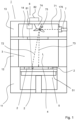
- FIG. 1 shows an overview of an apparatus 1 for producing an object 2 by means of additive manufacturing.
- the apparatus 1 is build from several frame parts 11, 12, 13.
- the apparatus comprises a process chamber 3 for receiving a bath of material 4 which can be solidified.
- a shaft is formed, wherein a support 5 is provided for positioning the object 2 (or even objects) in relation to the surface level L of the bath of material 4.
- the support 5 is movably provided in the shaft, such that after solidifying a layer, the support 5 may be lowered, and a further layer of material may be solidified on top of the part of the object 2 already formed.
- a solidifying device 7 is provided for solidifying a selective part of the material.
- the solidifying device 7 is a laser device, which is arranged for producing electromagnetic radiation in the form of laser light 71, in order to melt a powdered material provided on the support, which then, after cooling forms a solidified part of the object to be produced.
- the invention is not limited to the type of solidifying device.
- the electromagnetic radiation 71 emitted by the laser device 7 is deflected by means of a deflector unit 74, which uses a rotatable optical element 75, e.g. one or more galvo mirror elements 75, to direct the emitted radiation 71 towards the surface L of the layer of material 4.
- the apparatus comprises an optical control device 176 with a focus unit provided in an optical pathway of the electromagnetic radiation of the solidifying device 7, and arranged for controlling at least the focus of the electromagnetic radiation emitted by the solidifying device on the surface level.
- the focus unit has at least one focus element 76 (see Fig. 2 ), which may be used to adjust the focus of the radiation, for example for adjusting for the increased distance covered by ray 72 compared to ray 73.
- the apparatus 1 may further comprise a recoating device (not shown) which can be displaced along the surface L of the bath for levelling the surface L of the bath of material 4.
- a recoating device is known per se to those skilled in the art.
- focus calibration is aimed at providing accurate focus on the surface L of the bath, since this is the surface level where the solidifying device needs to present accurate focus for solidifying material.
- Fig. 2 shows a schematic detail of the laser beam 71, the rotatable optical element 75, and the radiation directed towards the surface L of the layer of material 4.
- rays 73 and 72 show the radiation for different angular positions of the rotatable optical element 75. Due to the fact that a rotatable optical element 75 is used, a generally curved focal plane 79 is obtained.
- the build plate 51 (and the layer L of material 4) is a planar surface, and thus for a given position x s there will be a focus offset ⁇ z along the optical axis.
- Fig. 3 shows a first embodiment of a focus drift control device 9 according to the invention.
- Fig. 3 shows the solidifying device 7, emitting a beam 70, 71, 73 of electromagnetic radiation, onto the surface level L of the bath of material.
- a focus unit 176 is used to ensure correct focus of the beam.
- the focus unit 176 comprises a collimating lens 91, and a focus objective lens 76.
- the deflector unit 74 comprises two rotatable optical elements 75a, 75b that are used to direct the beam towards the desired xy-position.
- a focus drift control device 9 comprises a sensor element 95 arranged for detecting a measure for the accuracy of the focus of the electromagnetic radiation, a focus correction lens element 93 provided in the optical pathway of the electromagnetic radiation, and arranged to be movable (in housing 63) in the direction of at least an optical axis thereof; and a focus correction control unit 97, connected to said sensor element 95 via line 96 and to said focus correction element 93 via line 64, and arranged for moving said focus correction lens element 63 in response to a signal obtained by said sensor element 95.
- a focus correction control unit 97 connected to said sensor element 95 via line 96 and to said focus correction element 93 via line 64, and arranged for moving said focus correction lens element 63 in response to a signal obtained by said sensor element 95.
- the focus correction control unit 97 is arranged for receiving system information 99 and/or system data 99 of said apparatus, and is arranged for moving said focus correction lens element 93 in response to said system information 99 and/or said system data 99 of said apparatus.
- Said system information may for example be temperature information of the apparatus, or may contain operating parameters.
- Fig. 4 shows an alternative embodiment of the device 9 shown in Fig. 3 , in which some modifications with respect to placement of the sensor element 95 have been made. For reasons of conciseness it will be focused on the main differences. Same or similar components are indicated with the same reference sign.
- the beam splitter element 61b is provided more downstream in the optical path.
- the beam splitter element 61b is provided downstream of the deflector unit 74. This way, changes in temperature affecting the deflector unit 74, the optical element 76, and all further upstream components may be sensed by the sensor element 95, allowing compensation for these effects.
- a mirror 61a is used to deflect the beam from the solidifying device, although it is conceivable of course that the mirror 61a is eliminated completely, and the solidifying device 7 and collimating lens 91 are placed in line.
Landscapes
- Engineering & Computer Science (AREA)
- Chemical & Material Sciences (AREA)
- Materials Engineering (AREA)
- Manufacturing & Machinery (AREA)
- Physics & Mathematics (AREA)
- Optics & Photonics (AREA)
- Mechanical Engineering (AREA)
- Toxicology (AREA)
- Health & Medical Sciences (AREA)
- Plasma & Fusion (AREA)
- General Health & Medical Sciences (AREA)
- Analytical Chemistry (AREA)
- Automation & Control Theory (AREA)
Description
- The invention relates to an apparatus for producing an object by means of additive manufacturing, comprising a process chamber for receiving a bath of material which can be solidified by exposure to electromagnetic radiation; a support for positioning the object in relation to the surface level of the bath of material; and a solidifying device for solidifying a layer of the material on the surface level by means of electromagnetic radiation.
- 3D printing or additive manufacturing refers to any of various processes for manufacturing a three-dimensional object. Traditional techniques like injection molding can be less expensive for manufacturing, for example, polymer products in high quantities, but 3D printing or additive manufacturing can be faster, more flexible and less expensive when producing relatively small quantities of three-dimensional objects.
- It is anticipated that additive manufacturing becomes more and more important in the future, as the increasing competitive pressure forces companies to not only manufacture more economically with a constant high product quality but also to save time and costs in the area of product development. The life span of products is continuously shortened. In addition to product quality and product costs, the moment of market introduction is becoming increasingly important for the success of a product.
- The three-dimensional object may be produced by selectively solidifying, in a layer-like fashion, a powder, paper or sheet material to produce a three-dimensional, 3D, object. In particular, a computer controlled additive manufacturing apparatus may be used which sequentially sinters a plurality of layers to build the desired object in a layer-by-layer fashion. Primarily additive processes are used, in which successive layers of material are laid down under computer control. These objects can be of almost any shape or geometry, and are produced from a 3D model or other electronic data source.
- In order to print a three-dimensional object, a printable model is to be created with a computer design package or via a 3D scanner, for example. Usually, the input is a 3D CAD file such as an STL file, a STEP file or a IGS file. Before printing the object from a CAD file, the file is to be processed by a piece of software, which converts the model into a series of thin subsequent layers. Further, apparatus settings and vectors are generated for controlling the creation of each of the subsequent layers.
- A laser comprised in the computer controlled additive manufacturing apparatus follows these settings and vectors to solidify successive layers of material to built the 3D object from a series of cross sections. These layers, which correspond to the virtual cross sections from the CAD model, are during this process joined or fused at the same time to create the final 3D object.
-
WO 2017/051168 A1 andJP2009113293A - One of the challenges in the manufacturing of three dimensional objects, in particular in additive manufacturing of metal objects, is how to accurately and reproducibly solidify selective parts of the layer.
- To this end, the invention provides an apparatus for producing an object by means of additive manufacturing, comprising a process chamber for receiving a bath of material which can be solidified by exposure to electromagnetic radiation; a support for positioning the object in relation to the surface level of the bath of material; and a solidifying device for solidifying a selective layer-part of the material on the surface level by means of electromagnetic radiation.
- Additionally, the apparatus according to the invention comprises an optical control device with a focus unit provided in an optical pathway of the electromagnetic radiation of the solidifying device, and arranged for controlling at least the focus of the electromagnetic radiation emitted by the solidifying device on the surface level. Said focus unit may comprise one or more lens elements, or one or more lens objectives, and is arranged for controlling the focus of the electromagnetic radiation on a focal plane (i.e. the surface level of the bath of material).
- According to the invention the optical control device comprises a sensor element arranged for detecting a measure for the accuracy of the focus of the electromagnetic radiation. The sensor element preferably is an inline focus sensor, meaning that it is arranged to be in contact with the electromagnetic radiation.
- Furthermore, a focus correction lens element is provided in the optical pathway of the electromagnetic radiation. This focus correction lens element is preferably an individual element, meaning that it is arranged separately from the focus unit, in particular downstream or upstream of the focus unit. The focus correction lens element is arranged to be movable in the direction of at least an optical axis thereof. Hence, the overall focus of the electromagnetic radiation on the focal plane may be changed or adjusted by moving the focus correction lens element. The focus correction lens element may be a single lens element, or may be part of a more complex objective lens.
- Additionally, the apparatus according to the invention comprises a focus correction control unit, connected to said sensor element and to said focus correction element, and arranged for moving said focus correction lens element in response to a signal obtained by said sensor element.
- With the apparatus according to the invention, it is possible to provide, in an easy and effective manner, for active compensation of focus drift due to thermo-mechanical and thermo-optical behaviour of optical components. It was found that heating up of optical elements by absorption of laser light can cause changes in focus characteristics. In particular, thermal expansion and change of refractive index with temperature are among the driving influences. These changes in focus, as a result of focus drift, causes variation in product quality. With the inline sensor element, coupled to a focus correction control unit, and the focus correction lens element it is possible to provide a correction for these changes in focus characteristics. With this, more accurate and reproducible production of solidified parts becomes possible. Thus, the object of the invention is achieved.
- Further advantageous embodiments of the invention will be described below.
- According to the invention, the optical control device comprises a beamsplitter element provided in the optical pathway of the electromagnetic radiation, and arranged for providing a beam of transmitted light and a beam of reflected light, and wherein the sensor element is arranged downstream of the beamsplitter element. With this it is possible to measure the accuracy of the focus with respect to the beam of electromagnetic radiation itself. Hence, the influence of thermal behaviour of optical components, in particular upstream of the beamsplitter element located on the transmitted optical pathway, can be sensed. Measures may be taken, i.e. focus may be corrected, when deviations are measure by the sensor element.
- In an embodiment, the sensor element is arranged to receive said beam of transmitted light. In that case, the reflected light is used as electromagnetic radiation for solidifying a part of the material on the surface level of the bath.
- In an effective embodiment, the beamsplitter element is a plane surface beamsplitter with partially transmitting or dichroic surface coating. This is an effective and accurate way to obtain a beam of reflected light and a beam of transmitted light.
- In an embodiment, the focus correction lens element is arranged upstream of the sensor element. This way, a direct feedback may be obtained: a deviation measured by the sensor element is used to adjust the focus correction lens element, and the resulting change in focus is once again measured by the sensor element.
- In an alternative embodiment, the focus correction lens element is arranged downstream of the sensor element. This may provide for a very compact construction, but this also means that hardly any feedback is obtained with respect to changes in focus as a result of movement of the focus correction lens element. In this embodiment, however, it can be ascertained that any deviation or change measured in the sensor element is the result of thermal behaviour of the optical components upstream of the beamsplitter, and not the result, for example, of an inaccuracy of the focus correction lens element. Thus, this provides more reliable information with regards to the thermal situation of the apparatus.
- In an embodiment, the focus correction lens is arranged in the optical path of the beam of reflected light. In particular, the focus correction lens is arranged in between said beamsplitter element and said focus unit. In other words, the focus correction lens is provided downstream of said beamsplitter element, and upstream of said focus unit.
- To further increase the accuracy of focus of the apparatus, the focus correction control unit may be arranged for receiving system information and/or system data of said apparatus. Said system information and/or system data may comprise one or more parameters of one or more parts of the apparatus, for example the solidifying device and/or the build chamber or parts thereof. Said one or more parameters may comprise geometry information, a temperature, a power usage, an active time, and/or an idle time, for example. Other parameters are conceivable as well. In this embodiment, the focus correction control unit is arranged for moving said focus correction lens element in response to said system information and/or said system data of said apparatus.
- In an embodiment, the focus correction lens element comprises a positive or negative lens, in particular a single positive or negative lens. This makes the overall construction relatively compact.
- In an embodiment, the optical control device comprises a positive lens element arranged upstream of said sensor element. The lens element is arranged for focusing electromagnetic radiation (either originating from reflection or transmission, but preferably originating from transmission) onto the sensor element. The lens element is arranged in such a way that in a standard condition the electromagnetic radiation is substantially perfectly focussed on the sensor element. The lens element is in particular a fixed, i.e. non-movable, lens element.
- According to an aspect, the invention provides a method of correcting a focus of electromagnetic radiation on a surface level of a bath of material which can be solidified by exposure to said electromagnetic radiation, wherein said method comprises the steps of:
- providing a beam of electromagnetic radiation;
- focusing said beam of electromagnetic radiation on said surface level of the bath of material by using a focus unit provided in an optical path of the electromagnetic radiation;
- detecting a measure for the accuracy of the focus of the electromagnetic radiation; and
- moving a focus correction lens element in response to the detected measure for the accuracy of the focus of the electromagnetic radiation for correcting the focus.
- The method according to the invention comprises the step of using an apparatus according to the invention, in particular as described above.
- With the method, it is possible to provide active compensation of focus drift as a result of thermal behaviour of optical components in the apparatus. Further advantages of the method have already been discussed with respect to the apparatus.
- The invention will next be explained by means of the accompanying figures. In the figures:
-
Fig. 1 - shows a schematic overview of an apparatus according to the invention, arranged for producing an object by means of additive manufacturing; -
Fig. 2 - shows a schematic overview of the electromagnetic radiation emitted by the solidifying device, via the rotatable deflector unit, onto the bath of material; -
Fig. 3 - schematically shows an overview of an optical control device according to a first embodiment of the invention; -
Fig. 4 - schematically shows an overview of an optical control device according to a second embodiment of the invention; -
Fig. 5 - shows an alternative embodiment to the set up ofFig. 4 and which is not according to the present invention. -
Figure 1 shows an overview of anapparatus 1 for producing anobject 2 by means of additive manufacturing. Theapparatus 1 is build fromseveral frame parts process chamber 3 for receiving a bath ofmaterial 4 which can be solidified. In alower frame part 11, a shaft is formed, wherein asupport 5 is provided for positioning the object 2 (or even objects) in relation to the surface level L of the bath ofmaterial 4. Thesupport 5 is movably provided in the shaft, such that after solidifying a layer, thesupport 5 may be lowered, and a further layer of material may be solidified on top of the part of theobject 2 already formed. In atop part 13 of theapparatus 1, a solidifyingdevice 7 is provided for solidifying a selective part of the material. In the embodiment shown, the solidifyingdevice 7 is a laser device, which is arranged for producing electromagnetic radiation in the form oflaser light 71, in order to melt a powdered material provided on the support, which then, after cooling forms a solidified part of the object to be produced. However, the invention is not limited to the type of solidifying device. As can be seen, theelectromagnetic radiation 71 emitted by thelaser device 7 is deflected by means of adeflector unit 74, which uses a rotatableoptical element 75, e.g. one or moregalvo mirror elements 75, to direct the emittedradiation 71 towards the surface L of the layer ofmaterial 4. Depending on the position of thedeflector unit 74, radiation may be emitted, as an example, according torays optical control device 176 with a focus unit provided in an optical pathway of the electromagnetic radiation of the solidifyingdevice 7, and arranged for controlling at least the focus of the electromagnetic radiation emitted by the solidifying device on the surface level. The focus unit has at least one focus element 76 (seeFig. 2 ), which may be used to adjust the focus of the radiation, for example for adjusting for the increased distance covered byray 72 compared toray 73. - The
apparatus 1 may further comprise a recoating device (not shown) which can be displaced along the surface L of the bath for levelling the surface L of the bath ofmaterial 4. Such a recoating device is known per se to those skilled in the art. With the method according to the invention, focus calibration is aimed at providing accurate focus on the surface L of the bath, since this is the surface level where the solidifying device needs to present accurate focus for solidifying material. - The
apparatus 1 may comprise acalibration system 8 with asensor unit 81. Thesensor unit 81 is directed to the surface level L of the layer ofmaterial 4, or -in absence of material 4- towards thesupport 5. Thecalibration system 8 is connected to theapparatus 1 by means ofline 82. With this, the calibration system may control the solidifying device, as will be explained below. Thecalibration system 8 may be a fixed part of theapparatus 1, or may be a more or less modular component that is connected to theapparatus 1 in case calibration of the apparatus is desired. Thesensor unit 81 may comprise an imaging sensor for making an image of the surface level L of the layer of material, or any other material presented on the support (such as a calibration body), or of thesupport 5 itself. This imaging sensor may also be arranged in such a way that the optical path of the imaging sensor coincides with the optical path of the solidifying device, or is generally the same thereto. This is referred to as an on-axis imaging sensor. -
Fig. 2 shows a schematic detail of thelaser beam 71, the rotatableoptical element 75, and the radiation directed towards the surface L of the layer ofmaterial 4. Here, rays 73 and 72 show the radiation for different angular positions of the rotatableoptical element 75. Due to the fact that a rotatableoptical element 75 is used, a generally curvedfocal plane 79 is obtained. The build plate 51 (and the layer L of material 4) is a planar surface, and thus for a given position xs there will be a focus offset δz along the optical axis. Hence, the geometrical set up of the solidifyingdevice 7, thedeflector unit 74, and thebuild plate 51 on thesupport 5 leads to a general focus offset, that may be compensated for by a so called general focus setting, which adjusts the focus based on a given x-position. The general focus settings may be incorporated into a look-up table, and may be used by the device to change focus depending on the position on the layer of material. This general focus setting is referred to as the '0'-setting for any given position. It will be apparent to those skilled in the art, that the actual focus setting of these '0'-setting may differ for different locations on the build plate, as it is the result of the geometrical set up. - Due to for instance, heating up of
optical elements 76 by absorption of laser light, the focus characteristics can change. In particular, thermal expansion and change of refractive index with temperature are among the driving influences. These changes in focus, as a result of focus drift, causes variation in product quality. To further improve the focus, in particular to compensate for so called focus drift due to changes in temperature, a focus correction lens and focus correction unit according to the invention may be applied. Two possible embodiments thereof are shown inFig. 3 and Fig. 4 . -
Fig. 3 shows a first embodiment of a focusdrift control device 9 according to the invention.Fig. 3 shows the solidifyingdevice 7, emitting abeam focus unit 176 is used to ensure correct focus of the beam. Thefocus unit 176 comprises acollimating lens 91, and afocus objective lens 76. Furthermore, thedeflector unit 74 comprises two rotatableoptical elements - It can be seen in
Fig. 3 that there is provided a focusdrift control device 9. Thisdevice 9 comprises asensor element 95 arranged for detecting a measure for the accuracy of the focus of the electromagnetic radiation, a focuscorrection lens element 93 provided in the optical pathway of the electromagnetic radiation, and arranged to be movable (in housing 63) in the direction of at least an optical axis thereof; and a focuscorrection control unit 97, connected to saidsensor element 95 vialine 96 and to saidfocus correction element 93 vialine 64, and arranged for moving said focuscorrection lens element 63 in response to a signal obtained by saidsensor element 95. As can be seen inFig. 3 ,lens element 63 is movably retained in thehousing 63, such that the lens element may move left and/or right to change the focus of thebeam 73 onto the surface L. Thesensor element 95 may be arranged for measuring the intensity of the beam received. The focuscorrection lens element 93 may comprise a single positive or negative lens. - In the embodiment shown in
Fig. 3 , abeamsplitter element 61 is provided in the optical pathway of the electromagnetic radiation 60, and arranged for providing a beam of transmitted light (going upward inFig. 3 ) and a beam of reflected light (going right inFig. 3 ). Thesensor element 95 is arranged downstream of thebeamsplitter element 61, and is arranged to receive said beam of transmitted light. This beamsplitter element may be a plane surface beamsplitter, in an embodiment. The focuscorrection lens element 93 is arranged downstream of thebeamsplitter element 61 and is arranged in the optical path of the beam of reflected light. The embodiment shown inFig. 3 may be very compact, as thefocus correction lens 93 is arranged in between saidbeamsplitter element 61 and saidfocus unit 76. - Additionally, the focus
correction control unit 97 is arranged for receivingsystem information 99 and/orsystem data 99 of said apparatus, and is arranged for moving said focuscorrection lens element 93 in response to saidsystem information 99 and/or saidsystem data 99 of said apparatus. Said system information may for example be temperature information of the apparatus, or may contain operating parameters. -
Fig. 4 shows an alternative embodiment of thedevice 9 shown inFig. 3 , in which some modifications with respect to placement of thesensor element 95 have been made. For reasons of conciseness it will be focused on the main differences. Same or similar components are indicated with the same reference sign. InFig. 4 it can be seen that thebeam splitter element 61b is provided more downstream in the optical path. Thebeam splitter element 61b is provided downstream of thedeflector unit 74. This way, changes in temperature affecting thedeflector unit 74, theoptical element 76, and all further upstream components may be sensed by thesensor element 95, allowing compensation for these effects. InFig. 4 amirror 61a is used to deflect the beam from the solidifying device, although it is conceivable of course that themirror 61a is eliminated completely, and the solidifyingdevice 7 andcollimating lens 91 are placed in line. - The
focus correction lens 93 is still provided upstream of theoptical element 76, but now that thesensor element 95 is provided downstream of thefocus correction lens 93, a positive feedback control loop is possible, which is something that is difficult to achieve with the setup ofFig. 3 . It is of course conceivable that thesensor element 95 is placed in a different part of the optical beam path, and that the focuscorrection lens element 93 is positioned in another part of the optical beam path. It is additionally, or alternatively conceivable that thesensor unit 81 of the calibration unit 8 (seeFig. 1 ) is used for detecting a measure for the accuracy of the focus of the electromagnetic radiation. Such asensor unit 81 may be an imaging unit, such as a camera. -
Fig. 5 shows an alternative embodiment which is not according to the invention, wherein the sensor element is positioned downstream of the surface level L. Thus in effect, light on the surface level L is reflected backwards to thebeam splitter element 61b and then passed onto thesensor element 95. This gives a possibility for a positive feedback control loop, such that the focus at the surface level L may be accurately controlled. - With the device and apparatus as described with respect to the figures, focus correction may be performed as follows. First, a
beam material 4 by using afocus unit 76 provided in an optical path of the electromagnetic radiation. Then a measure for the accuracy of the focus of the electromagnetic radiation is detected, using thesensor element 95. To correct the focus, the focuscorrection lens element 93 is moved in response to the detected measure for the accuracy of the focus of the electromagnetic radiation for correcting the focus. With this, focus of the beam is improved. The method uses the apparatus as defined by the present claims.
Claims (10)
- Apparatus (1) for producing an object (2) by means of additive manufacturing, comprising:- a process chamber (3) for receiving a bath (4) of material which can be solidified by exposure to electromagnetic radiation;- a support (5) for positioning the object in relation to the surface level (L) of the bath of material;- a solidifying device (7) for solidifying a selective layer-part of the material on the surface level (L) by means of electromagnetic radiation; and- an optical control device (176) with a focus unit (76) provided in an optical pathway of the electromagnetic radiation of the solidifying device (7), and arranged for controlling at least the focus of the electromagnetic radiation emitted by the solidifying device (7) on the surface level;wherein the optical control device (176) comprises:- a sensor element (95) arranged for detecting a measure for the accuracy of the focus of the electromagnetic radiation, wherein the sensor element (95) is arranged upstream of the surface level (L);- a focus correction lens element (93) provided in the optical pathway of the electromagnetic radiation, and arranged to be movable in the direction of at least an optical axis thereof; and- a focus correction control unit (97), connected to said sensor element (95) and to said focus correction element (93), and arranged for moving said focus correction lens element (93) in response to a signal obtained by said sensor element (95)- a beamsplitter element (61) provided in the optical pathway of the electromagnetic radiation, and arranged for providing a beam of transmitted light and a beam of reflected light, and wherein the sensor element (95) is arranged downstream of the beamsplitter element (61).
- Apparatus according to claim 1, wherein the sensor element (95) is arranged to receive said beam of transmitted light.
- Apparatus according to claim 1 or 2, wherein the beamsplitter element (61) is a plane surface beamsplitter.
- Apparatus according to claim 1-3, wherein the focus correction lens element (93) is arranged downstream of the beamsplitter element (61).
- Apparatus according to claim 2 and 4, wherein the focus correction lens element (93) is arranged in the optical path of the beam of reflected light.
- Apparatus according to claim 5, wherein the focus correction lens element (93) is arranged in between said beamsplitter element (61) and said focus unit (76).
- Apparatus according to any one of the previous claims, wherein the focus correction control unit (97) is arranged for receiving system information (99) and/or system data (99) of said apparatus, and is arranged for moving said focus correction lens element (93) in response to said system information and/or said system data of said apparatus.
- Apparatus according to any one of the previous claims, wherein the focus correction lens element (93) comprises a positive or negative lens.
- Apparatus according to any one of the previous claims, wherein the optical control device (176) comprises a positive lens element (92) arranged upstream of said sensor element (95).
- Method of correcting a focus of electromagnetic radiation on a surface level (L) of a bath of material (4) which can be solidified by exposure to said electromagnetic radiation using an apparatus according to any one of the previous claims, wherein said method comprises the steps of:- providing a beam of electromagnetic radiation (70, 71, 72, 73);- focusing said beam of electromagnetic radiation on said surface level (L) of the bath of material by using a focus unit (176) provided in an optical path of the electromagnetic radiation;- detecting a measure for the accuracy of the focus of the electromagnetic radiation;- moving a focus correction lens element (93) in response to the detected measure for the accuracy of the focus of the electromagnetic radiation for correcting the focus.
Applications Claiming Priority (2)
| Application Number | Priority Date | Filing Date | Title |
|---|---|---|---|
| NL2019998A NL2019998B1 (en) | 2017-11-30 | 2017-11-30 | Apparatus for producing an object by means of additive manufacturing |
| PCT/NL2018/050790 WO2019108058A1 (en) | 2017-11-30 | 2018-11-26 | Apparatus and method for producing an object by means of additive manufacturing |
Publications (2)
| Publication Number | Publication Date |
|---|---|
| EP3717205A1 EP3717205A1 (en) | 2020-10-07 |
| EP3717205B1 true EP3717205B1 (en) | 2024-07-10 |
Family
ID=60628147
Family Applications (1)
| Application Number | Title | Priority Date | Filing Date |
|---|---|---|---|
| EP18839756.6A Active EP3717205B1 (en) | 2017-11-30 | 2018-11-26 | Apparatus and method for producing an object by means of additive manufacturing |
Country Status (6)
| Country | Link |
|---|---|
| US (1) | US11518099B2 (en) |
| EP (1) | EP3717205B1 (en) |
| JP (1) | JP7248679B2 (en) |
| CN (1) | CN111465484B (en) |
| NL (1) | NL2019998B1 (en) |
| WO (1) | WO2019108058A1 (en) |
Families Citing this family (2)
| Publication number | Priority date | Publication date | Assignee | Title |
|---|---|---|---|---|
| US12151309B1 (en) * | 2019-01-31 | 2024-11-26 | Freeform Future Corp. | Clustered laser-beam steering for metal additive manufacturing using powder-bed fusion |
| US20230122506A1 (en) * | 2021-10-14 | 2023-04-20 | Layerwise Nv | Three-Dimensional Printing System with Offset Flat Field Unit |
Citations (3)
| Publication number | Priority date | Publication date | Assignee | Title |
|---|---|---|---|---|
| JP2009113293A (en) * | 2007-11-05 | 2009-05-28 | Sony Corp | Stereolithography apparatus and stereolithography method |
| US9597835B2 (en) * | 2011-05-16 | 2017-03-21 | Sony Corporation | Three-dimensional modeling apparatus, model, and method of manufacturing a model |
| EP3202525A1 (en) * | 2016-02-02 | 2017-08-09 | XYZprinting, Inc. | Three-dimensional object generating apparatus and method for calibrating thereof |
Family Cites Families (8)
| Publication number | Priority date | Publication date | Assignee | Title |
|---|---|---|---|---|
| JP5018076B2 (en) * | 2006-12-22 | 2012-09-05 | ソニー株式会社 | Stereolithography apparatus and stereolithography method |
| JP5234319B2 (en) * | 2008-01-21 | 2013-07-10 | ソニー株式会社 | Stereolithography apparatus and stereolithography method |
| GB201316815D0 (en) | 2013-09-23 | 2013-11-06 | Renishaw Plc | Additive manufacturing apparatus and method |
| US11458539B2 (en) * | 2014-11-24 | 2022-10-04 | Additive Industries B.V. | Apparatus for producing an object by means of additive manufacturing |
| DE102014226243A1 (en) * | 2014-12-17 | 2016-06-23 | MTU Aero Engines AG | Device for the generative production of a component |
| DE102015000102A1 (en) * | 2015-01-14 | 2016-07-14 | Cl Schutzrechtsverwaltungs Gmbh | Device for the generative production of three-dimensional components |
| GB201516681D0 (en) * | 2015-09-21 | 2015-11-04 | Renishaw Plc | Addictive manufacturing apparatus and an optical module for use in an addictive manufacturing apparatus |
| US20180186080A1 (en) * | 2017-01-05 | 2018-07-05 | Velo3D, Inc. | Optics in three-dimensional printing |
-
2017
- 2017-11-30 NL NL2019998A patent/NL2019998B1/en active
-
2018
- 2018-11-26 WO PCT/NL2018/050790 patent/WO2019108058A1/en not_active Ceased
- 2018-11-26 CN CN201880065403.0A patent/CN111465484B/en active Active
- 2018-11-26 JP JP2020529610A patent/JP7248679B2/en active Active
- 2018-11-26 US US16/753,180 patent/US11518099B2/en active Active
- 2018-11-26 EP EP18839756.6A patent/EP3717205B1/en active Active
Patent Citations (3)
| Publication number | Priority date | Publication date | Assignee | Title |
|---|---|---|---|---|
| JP2009113293A (en) * | 2007-11-05 | 2009-05-28 | Sony Corp | Stereolithography apparatus and stereolithography method |
| US9597835B2 (en) * | 2011-05-16 | 2017-03-21 | Sony Corporation | Three-dimensional modeling apparatus, model, and method of manufacturing a model |
| EP3202525A1 (en) * | 2016-02-02 | 2017-08-09 | XYZprinting, Inc. | Three-dimensional object generating apparatus and method for calibrating thereof |
Also Published As
| Publication number | Publication date |
|---|---|
| US11518099B2 (en) | 2022-12-06 |
| WO2019108058A1 (en) | 2019-06-06 |
| NL2019998B1 (en) | 2019-06-07 |
| JP2021504198A (en) | 2021-02-15 |
| JP7248679B2 (en) | 2023-03-29 |
| US20200316863A1 (en) | 2020-10-08 |
| CN111465484A (en) | 2020-07-28 |
| CN111465484B (en) | 2022-02-25 |
| EP3717205A1 (en) | 2020-10-07 |
Similar Documents
| Publication | Publication Date | Title |
|---|---|---|
| EP3224025B1 (en) | Apparatus for producing an object by means of additive manufacturing and method for calibrating an apparatus | |
| JP7438726B2 (en) | Method for adjusting equipment for manufacturing objects using additive manufacturing technology and device for the method | |
| JP7153067B2 (en) | Method for adjusting equipment for manufacturing objects using additive manufacturing | |
| EP3562649B1 (en) | Sensor that simulates resin optical properties | |
| CN104216219B (en) | Imprinting apparatus, imprinting method and method of manufacturing a product | |
| JPH10505799A (en) | Method and apparatus for manufacturing a three-dimensional object | |
| KR101850222B1 (en) | Apparatus and method for correcting axial error of three-dimensional printer | |
| EP3202525B1 (en) | Three-dimensional object generating apparatus and method for calibrating thereof | |
| US11518099B2 (en) | Apparatus and method for producing an object by means of additive manufacturing | |
| KR101728876B1 (en) | An Apparatus Having a Structure of Automatic Focus Regulation and a Method for Marking with the Same | |
| US11850792B2 (en) | Method for calibrating an apparatus for producing an object by means of additive manufacturing, and apparatus for the method | |
| CN113661048B (en) | Method and device for producing an object by additive manufacturing | |
| JP7728981B2 (en) | Method and device for calibrating an illumination system, computer program product and apparatus for producing a three-dimensional workpiece - Patent Application 20070122997 | |
| CN118871232B (en) | Apparatus, system and method for calibrating a laser device | |
| NL2013861B1 (en) | Apparatus for producing an object by means of additive manufacturing. | |
| CN211074711U (en) | Projection type 3D printer | |
| WO2019052671A1 (en) | Method of calibrating an apparatus for generatively manufacturing a three-dimensional object | |
| US20220212259A1 (en) | Apparatus and Method for Producing an Object by Means of Additive Manufacturing |
Legal Events
| Date | Code | Title | Description |
|---|---|---|---|
| STAA | Information on the status of an ep patent application or granted ep patent |
Free format text: STATUS: UNKNOWN |
|
| STAA | Information on the status of an ep patent application or granted ep patent |
Free format text: STATUS: THE INTERNATIONAL PUBLICATION HAS BEEN MADE |
|
| PUAI | Public reference made under article 153(3) epc to a published international application that has entered the european phase |
Free format text: ORIGINAL CODE: 0009012 |
|
| STAA | Information on the status of an ep patent application or granted ep patent |
Free format text: STATUS: REQUEST FOR EXAMINATION WAS MADE |
|
| 17P | Request for examination filed |
Effective date: 20200406 |
|
| AK | Designated contracting states |
Kind code of ref document: A1 Designated state(s): AL AT BE BG CH CY CZ DE DK EE ES FI FR GB GR HR HU IE IS IT LI LT LU LV MC MK MT NL NO PL PT RO RS SE SI SK SM TR |
|
| AX | Request for extension of the european patent |
Extension state: BA ME |
|
| DAV | Request for validation of the european patent (deleted) | ||
| DAX | Request for extension of the european patent (deleted) | ||
| STAA | Information on the status of an ep patent application or granted ep patent |
Free format text: STATUS: EXAMINATION IS IN PROGRESS |
|
| 17Q | First examination report despatched |
Effective date: 20220104 |
|
| REG | Reference to a national code |
Ref country code: DE Ref legal event code: R079 Free format text: PREVIOUS MAIN CLASS: B29C0064264000 Ipc: B29C0064393000 Ref document number: 602018071669 Country of ref document: DE |
|
| RIC1 | Information provided on ipc code assigned before grant |
Ipc: B29C 64/264 20170101ALI20240328BHEP Ipc: B29C 64/153 20170101ALI20240328BHEP Ipc: B22F 10/20 20210101ALI20240328BHEP Ipc: B22F 10/30 20210101ALI20240328BHEP Ipc: B29C 64/268 20170101ALI20240328BHEP Ipc: B29C 64/393 20170101AFI20240328BHEP |
|
| GRAP | Despatch of communication of intention to grant a patent |
Free format text: ORIGINAL CODE: EPIDOSNIGR1 |
|
| STAA | Information on the status of an ep patent application or granted ep patent |
Free format text: STATUS: GRANT OF PATENT IS INTENDED |
|
| GRAS | Grant fee paid |
Free format text: ORIGINAL CODE: EPIDOSNIGR3 |
|
| INTG | Intention to grant announced |
Effective date: 20240510 |
|
| GRAA | (expected) grant |
Free format text: ORIGINAL CODE: 0009210 |
|
| STAA | Information on the status of an ep patent application or granted ep patent |
Free format text: STATUS: THE PATENT HAS BEEN GRANTED |
|
| AK | Designated contracting states |
Kind code of ref document: B1 Designated state(s): AL AT BE BG CH CY CZ DE DK EE ES FI FR GB GR HR HU IE IS IT LI LT LU LV MC MK MT NL NO PL PT RO RS SE SI SK SM TR |
|
| REG | Reference to a national code |
Ref country code: CH Ref legal event code: EP |
|
| P01 | Opt-out of the competence of the unified patent court (upc) registered |
Free format text: CASE NUMBER: APP_35615/2024 Effective date: 20240613 |
|
| REG | Reference to a national code |
Ref country code: DE Ref legal event code: R096 Ref document number: 602018071669 Country of ref document: DE |
|
| REG | Reference to a national code |
Ref country code: SE Ref legal event code: TRGR |
|
| REG | Reference to a national code |
Ref country code: NL Ref legal event code: FP |
|
| REG | Reference to a national code |
Ref country code: LT Ref legal event code: MG9D |
|
| PG25 | Lapsed in a contracting state [announced via postgrant information from national office to epo] |
Ref country code: PT Free format text: LAPSE BECAUSE OF FAILURE TO SUBMIT A TRANSLATION OF THE DESCRIPTION OR TO PAY THE FEE WITHIN THE PRESCRIBED TIME-LIMIT Effective date: 20241111 |
|
| REG | Reference to a national code |
Ref country code: AT Ref legal event code: MK05 Ref document number: 1701692 Country of ref document: AT Kind code of ref document: T Effective date: 20240710 |
|
| PGFP | Annual fee paid to national office [announced via postgrant information from national office to epo] |
Ref country code: LU Payment date: 20241126 Year of fee payment: 7 |
|
| PG25 | Lapsed in a contracting state [announced via postgrant information from national office to epo] |
Ref country code: PT Free format text: LAPSE BECAUSE OF FAILURE TO SUBMIT A TRANSLATION OF THE DESCRIPTION OR TO PAY THE FEE WITHIN THE PRESCRIBED TIME-LIMIT Effective date: 20241111 |
|
| PG25 | Lapsed in a contracting state [announced via postgrant information from national office to epo] |
Ref country code: NO Free format text: LAPSE BECAUSE OF FAILURE TO SUBMIT A TRANSLATION OF THE DESCRIPTION OR TO PAY THE FEE WITHIN THE PRESCRIBED TIME-LIMIT Effective date: 20241010 |
|
| PG25 | Lapsed in a contracting state [announced via postgrant information from national office to epo] |
Ref country code: PL Free format text: LAPSE BECAUSE OF FAILURE TO SUBMIT A TRANSLATION OF THE DESCRIPTION OR TO PAY THE FEE WITHIN THE PRESCRIBED TIME-LIMIT Effective date: 20240710 Ref country code: FI Free format text: LAPSE BECAUSE OF FAILURE TO SUBMIT A TRANSLATION OF THE DESCRIPTION OR TO PAY THE FEE WITHIN THE PRESCRIBED TIME-LIMIT Effective date: 20240710 Ref country code: GR Free format text: LAPSE BECAUSE OF FAILURE TO SUBMIT A TRANSLATION OF THE DESCRIPTION OR TO PAY THE FEE WITHIN THE PRESCRIBED TIME-LIMIT Effective date: 20241011 |
|
| PGFP | Annual fee paid to national office [announced via postgrant information from national office to epo] |
Ref country code: BE Payment date: 20241120 Year of fee payment: 7 |
|
| PG25 | Lapsed in a contracting state [announced via postgrant information from national office to epo] |
Ref country code: BG Free format text: LAPSE BECAUSE OF FAILURE TO SUBMIT A TRANSLATION OF THE DESCRIPTION OR TO PAY THE FEE WITHIN THE PRESCRIBED TIME-LIMIT Effective date: 20240710 |
|
| PGFP | Annual fee paid to national office [announced via postgrant information from national office to epo] |
Ref country code: FR Payment date: 20241128 Year of fee payment: 7 |
|
| PG25 | Lapsed in a contracting state [announced via postgrant information from national office to epo] |
Ref country code: LV Free format text: LAPSE BECAUSE OF FAILURE TO SUBMIT A TRANSLATION OF THE DESCRIPTION OR TO PAY THE FEE WITHIN THE PRESCRIBED TIME-LIMIT Effective date: 20240710 |
|
| PG25 | Lapsed in a contracting state [announced via postgrant information from national office to epo] |
Ref country code: IS Free format text: LAPSE BECAUSE OF FAILURE TO SUBMIT A TRANSLATION OF THE DESCRIPTION OR TO PAY THE FEE WITHIN THE PRESCRIBED TIME-LIMIT Effective date: 20241110 Ref country code: AT Free format text: LAPSE BECAUSE OF FAILURE TO SUBMIT A TRANSLATION OF THE DESCRIPTION OR TO PAY THE FEE WITHIN THE PRESCRIBED TIME-LIMIT Effective date: 20240710 |
|
| PG25 | Lapsed in a contracting state [announced via postgrant information from national office to epo] |
Ref country code: HR Free format text: LAPSE BECAUSE OF FAILURE TO SUBMIT A TRANSLATION OF THE DESCRIPTION OR TO PAY THE FEE WITHIN THE PRESCRIBED TIME-LIMIT Effective date: 20240710 |
|
| PG25 | Lapsed in a contracting state [announced via postgrant information from national office to epo] |
Ref country code: RS Free format text: LAPSE BECAUSE OF FAILURE TO SUBMIT A TRANSLATION OF THE DESCRIPTION OR TO PAY THE FEE WITHIN THE PRESCRIBED TIME-LIMIT Effective date: 20241010 Ref country code: ES Free format text: LAPSE BECAUSE OF FAILURE TO SUBMIT A TRANSLATION OF THE DESCRIPTION OR TO PAY THE FEE WITHIN THE PRESCRIBED TIME-LIMIT Effective date: 20240710 |
|
| PGFP | Annual fee paid to national office [announced via postgrant information from national office to epo] |
Ref country code: SE Payment date: 20241120 Year of fee payment: 7 |
|
| PG25 | Lapsed in a contracting state [announced via postgrant information from national office to epo] |
Ref country code: RS Free format text: LAPSE BECAUSE OF FAILURE TO SUBMIT A TRANSLATION OF THE DESCRIPTION OR TO PAY THE FEE WITHIN THE PRESCRIBED TIME-LIMIT Effective date: 20241010 Ref country code: PL Free format text: LAPSE BECAUSE OF FAILURE TO SUBMIT A TRANSLATION OF THE DESCRIPTION OR TO PAY THE FEE WITHIN THE PRESCRIBED TIME-LIMIT Effective date: 20240710 Ref country code: NO Free format text: LAPSE BECAUSE OF FAILURE TO SUBMIT A TRANSLATION OF THE DESCRIPTION OR TO PAY THE FEE WITHIN THE PRESCRIBED TIME-LIMIT Effective date: 20241010 Ref country code: LV Free format text: LAPSE BECAUSE OF FAILURE TO SUBMIT A TRANSLATION OF THE DESCRIPTION OR TO PAY THE FEE WITHIN THE PRESCRIBED TIME-LIMIT Effective date: 20240710 Ref country code: IS Free format text: LAPSE BECAUSE OF FAILURE TO SUBMIT A TRANSLATION OF THE DESCRIPTION OR TO PAY THE FEE WITHIN THE PRESCRIBED TIME-LIMIT Effective date: 20241110 Ref country code: HR Free format text: LAPSE BECAUSE OF FAILURE TO SUBMIT A TRANSLATION OF THE DESCRIPTION OR TO PAY THE FEE WITHIN THE PRESCRIBED TIME-LIMIT Effective date: 20240710 Ref country code: GR Free format text: LAPSE BECAUSE OF FAILURE TO SUBMIT A TRANSLATION OF THE DESCRIPTION OR TO PAY THE FEE WITHIN THE PRESCRIBED TIME-LIMIT Effective date: 20241011 Ref country code: FI Free format text: LAPSE BECAUSE OF FAILURE TO SUBMIT A TRANSLATION OF THE DESCRIPTION OR TO PAY THE FEE WITHIN THE PRESCRIBED TIME-LIMIT Effective date: 20240710 Ref country code: ES Free format text: LAPSE BECAUSE OF FAILURE TO SUBMIT A TRANSLATION OF THE DESCRIPTION OR TO PAY THE FEE WITHIN THE PRESCRIBED TIME-LIMIT Effective date: 20240710 Ref country code: BG Free format text: LAPSE BECAUSE OF FAILURE TO SUBMIT A TRANSLATION OF THE DESCRIPTION OR TO PAY THE FEE WITHIN THE PRESCRIBED TIME-LIMIT Effective date: 20240710 Ref country code: AT Free format text: LAPSE BECAUSE OF FAILURE TO SUBMIT A TRANSLATION OF THE DESCRIPTION OR TO PAY THE FEE WITHIN THE PRESCRIBED TIME-LIMIT Effective date: 20240710 |
|
| PGFP | Annual fee paid to national office [announced via postgrant information from national office to epo] |
Ref country code: CH Payment date: 20241201 Year of fee payment: 7 |
|
| REG | Reference to a national code |
Ref country code: DE Ref legal event code: R097 Ref document number: 602018071669 Country of ref document: DE |
|
| PG25 | Lapsed in a contracting state [announced via postgrant information from national office to epo] |
Ref country code: SM Free format text: LAPSE BECAUSE OF FAILURE TO SUBMIT A TRANSLATION OF THE DESCRIPTION OR TO PAY THE FEE WITHIN THE PRESCRIBED TIME-LIMIT Effective date: 20240710 Ref country code: DK Free format text: LAPSE BECAUSE OF FAILURE TO SUBMIT A TRANSLATION OF THE DESCRIPTION OR TO PAY THE FEE WITHIN THE PRESCRIBED TIME-LIMIT Effective date: 20240710 Ref country code: RO Free format text: LAPSE BECAUSE OF FAILURE TO SUBMIT A TRANSLATION OF THE DESCRIPTION OR TO PAY THE FEE WITHIN THE PRESCRIBED TIME-LIMIT Effective date: 20240710 |
|
| PG25 | Lapsed in a contracting state [announced via postgrant information from national office to epo] |
Ref country code: EE Free format text: LAPSE BECAUSE OF FAILURE TO SUBMIT A TRANSLATION OF THE DESCRIPTION OR TO PAY THE FEE WITHIN THE PRESCRIBED TIME-LIMIT Effective date: 20240710 |
|
| PG25 | Lapsed in a contracting state [announced via postgrant information from national office to epo] |
Ref country code: CZ Free format text: LAPSE BECAUSE OF FAILURE TO SUBMIT A TRANSLATION OF THE DESCRIPTION OR TO PAY THE FEE WITHIN THE PRESCRIBED TIME-LIMIT Effective date: 20240710 |
|
| PG25 | Lapsed in a contracting state [announced via postgrant information from national office to epo] |
Ref country code: SK Free format text: LAPSE BECAUSE OF FAILURE TO SUBMIT A TRANSLATION OF THE DESCRIPTION OR TO PAY THE FEE WITHIN THE PRESCRIBED TIME-LIMIT Effective date: 20240710 |
|
| PLBE | No opposition filed within time limit |
Free format text: ORIGINAL CODE: 0009261 |
|
| STAA | Information on the status of an ep patent application or granted ep patent |
Free format text: STATUS: NO OPPOSITION FILED WITHIN TIME LIMIT |
|
| 26N | No opposition filed |
Effective date: 20250411 |
|
| PG25 | Lapsed in a contracting state [announced via postgrant information from national office to epo] |
Ref country code: MC Free format text: LAPSE BECAUSE OF FAILURE TO SUBMIT A TRANSLATION OF THE DESCRIPTION OR TO PAY THE FEE WITHIN THE PRESCRIBED TIME-LIMIT Effective date: 20240710 |
|
| PG25 | Lapsed in a contracting state [announced via postgrant information from national office to epo] |
Ref country code: IE Free format text: LAPSE BECAUSE OF NON-PAYMENT OF DUE FEES Effective date: 20241126 |
|
| PGFP | Annual fee paid to national office [announced via postgrant information from national office to epo] |
Ref country code: NL Payment date: 20251119 Year of fee payment: 8 |
|
| PGFP | Annual fee paid to national office [announced via postgrant information from national office to epo] |
Ref country code: DE Payment date: 20251119 Year of fee payment: 8 |
|
| PGFP | Annual fee paid to national office [announced via postgrant information from national office to epo] |
Ref country code: GB Payment date: 20251121 Year of fee payment: 8 |
|
| PGFP | Annual fee paid to national office [announced via postgrant information from national office to epo] |
Ref country code: IT Payment date: 20251125 Year of fee payment: 8 |
|
| PG25 | Lapsed in a contracting state [announced via postgrant information from national office to epo] |
Ref country code: HU Free format text: LAPSE BECAUSE OF FAILURE TO SUBMIT A TRANSLATION OF THE DESCRIPTION OR TO PAY THE FEE WITHIN THE PRESCRIBED TIME-LIMIT; INVALID AB INITIO Effective date: 20181126 |
|
| PG25 | Lapsed in a contracting state [announced via postgrant information from national office to epo] |
Ref country code: CY Free format text: LAPSE BECAUSE OF FAILURE TO SUBMIT A TRANSLATION OF THE DESCRIPTION OR TO PAY THE FEE WITHIN THE PRESCRIBED TIME-LIMIT; INVALID AB INITIO Effective date: 20181126 |