EP3716554A1 - Galvanic isolation circuit - Google Patents
Galvanic isolation circuit Download PDFInfo
- Publication number
- EP3716554A1 EP3716554A1 EP19166177.6A EP19166177A EP3716554A1 EP 3716554 A1 EP3716554 A1 EP 3716554A1 EP 19166177 A EP19166177 A EP 19166177A EP 3716554 A1 EP3716554 A1 EP 3716554A1
- Authority
- EP
- European Patent Office
- Prior art keywords
- transceiver
- galvanic isolation
- link
- capacitor
- isolation circuit
- Prior art date
- Legal status (The legal status is an assumption and is not a legal conclusion. Google has not performed a legal analysis and makes no representation as to the accuracy of the status listed.)
- Granted
Links
Images




Classifications
-
- H—ELECTRICITY
- H04—ELECTRIC COMMUNICATION TECHNIQUE
- H04L—TRANSMISSION OF DIGITAL INFORMATION, e.g. TELEGRAPHIC COMMUNICATION
- H04L25/00—Baseband systems
- H04L25/02—Details ; arrangements for supplying electrical power along data transmission lines
- H04L25/0264—Arrangements for coupling to transmission lines
- H04L25/0266—Arrangements for providing Galvanic isolation, e.g. by means of magnetic or capacitive coupling
-
- H—ELECTRICITY
- H03—ELECTRONIC CIRCUITRY
- H03H—IMPEDANCE NETWORKS, e.g. RESONANT CIRCUITS; RESONATORS
- H03H7/00—Multiple-port networks comprising only passive electrical elements as network components
- H03H7/01—Frequency selective two-port networks
-
- H—ELECTRICITY
- H01—ELECTRIC ELEMENTS
- H01M—PROCESSES OR MEANS, e.g. BATTERIES, FOR THE DIRECT CONVERSION OF CHEMICAL ENERGY INTO ELECTRICAL ENERGY
- H01M10/00—Secondary cells; Manufacture thereof
- H01M10/42—Methods or arrangements for servicing or maintenance of secondary cells or secondary half-cells
- H01M10/4207—Methods or arrangements for servicing or maintenance of secondary cells or secondary half-cells for several batteries or cells simultaneously or sequentially
-
- H—ELECTRICITY
- H01—ELECTRIC ELEMENTS
- H01M—PROCESSES OR MEANS, e.g. BATTERIES, FOR THE DIRECT CONVERSION OF CHEMICAL ENERGY INTO ELECTRICAL ENERGY
- H01M10/00—Secondary cells; Manufacture thereof
- H01M10/42—Methods or arrangements for servicing or maintenance of secondary cells or secondary half-cells
- H01M10/425—Structural combination with electronic components, e.g. electronic circuits integrated to the outside of the casing
- H01M10/4257—Smart batteries, e.g. electronic circuits inside the housing of the cells or batteries
-
- H—ELECTRICITY
- H01—ELECTRIC ELEMENTS
- H01M—PROCESSES OR MEANS, e.g. BATTERIES, FOR THE DIRECT CONVERSION OF CHEMICAL ENERGY INTO ELECTRICAL ENERGY
- H01M10/00—Secondary cells; Manufacture thereof
- H01M10/42—Methods or arrangements for servicing or maintenance of secondary cells or secondary half-cells
- H01M10/48—Accumulators combined with arrangements for measuring, testing or indicating the condition of cells, e.g. the level or density of the electrolyte
-
- H—ELECTRICITY
- H03—ELECTRONIC CIRCUITRY
- H03H—IMPEDANCE NETWORKS, e.g. RESONANT CIRCUITS; RESONATORS
- H03H7/00—Multiple-port networks comprising only passive electrical elements as network components
- H03H7/01—Frequency selective two-port networks
- H03H7/0115—Frequency selective two-port networks comprising only inductors and capacitors
-
- H—ELECTRICITY
- H04—ELECTRIC COMMUNICATION TECHNIQUE
- H04B—TRANSMISSION
- H04B10/00—Transmission systems employing electromagnetic waves other than radio-waves, e.g. infrared, visible or ultraviolet light, or employing corpuscular radiation, e.g. quantum communication
- H04B10/40—Transceivers
-
- H—ELECTRICITY
- H04—ELECTRIC COMMUNICATION TECHNIQUE
- H04L—TRANSMISSION OF DIGITAL INFORMATION, e.g. TELEGRAPHIC COMMUNICATION
- H04L25/00—Baseband systems
- H04L25/38—Synchronous or start-stop systems, e.g. for Baudot code
- H04L25/40—Transmitting circuits; Receiving circuits
- H04L25/49—Transmitting circuits; Receiving circuits using code conversion at the transmitter; using predistortion; using insertion of idle bits for obtaining a desired frequency spectrum; using three or more amplitude levels ; Baseband coding techniques specific to data transmission systems
- H04L25/4917—Transmitting circuits; Receiving circuits using code conversion at the transmitter; using predistortion; using insertion of idle bits for obtaining a desired frequency spectrum; using three or more amplitude levels ; Baseband coding techniques specific to data transmission systems using multilevel codes
-
- H—ELECTRICITY
- H05—ELECTRIC TECHNIQUES NOT OTHERWISE PROVIDED FOR
- H05K—PRINTED CIRCUITS; CASINGS OR CONSTRUCTIONAL DETAILS OF ELECTRIC APPARATUS; MANUFACTURE OF ASSEMBLAGES OF ELECTRICAL COMPONENTS
- H05K1/00—Printed circuits
- H05K1/02—Details
- H05K1/0213—Electrical arrangements not otherwise provided for
- H05K1/0216—Reduction of cross-talk, noise or electromagnetic interference
- H05K1/023—Reduction of cross-talk, noise or electromagnetic interference using auxiliary mounted passive components or auxiliary substances
- H05K1/0231—Capacitors or dielectric substances
-
- H—ELECTRICITY
- H01—ELECTRIC ELEMENTS
- H01M—PROCESSES OR MEANS, e.g. BATTERIES, FOR THE DIRECT CONVERSION OF CHEMICAL ENERGY INTO ELECTRICAL ENERGY
- H01M10/00—Secondary cells; Manufacture thereof
- H01M10/42—Methods or arrangements for servicing or maintenance of secondary cells or secondary half-cells
- H01M10/425—Structural combination with electronic components, e.g. electronic circuits integrated to the outside of the casing
- H01M2010/4271—Battery management systems including electronic circuits, e.g. control of current or voltage to keep battery in healthy state, cell balancing
-
- H—ELECTRICITY
- H01—ELECTRIC ELEMENTS
- H01M—PROCESSES OR MEANS, e.g. BATTERIES, FOR THE DIRECT CONVERSION OF CHEMICAL ENERGY INTO ELECTRICAL ENERGY
- H01M10/00—Secondary cells; Manufacture thereof
- H01M10/42—Methods or arrangements for servicing or maintenance of secondary cells or secondary half-cells
- H01M10/425—Structural combination with electronic components, e.g. electronic circuits integrated to the outside of the casing
- H01M2010/4278—Systems for data transfer from batteries, e.g. transfer of battery parameters to a controller, data transferred between battery controller and main controller
-
- Y—GENERAL TAGGING OF NEW TECHNOLOGICAL DEVELOPMENTS; GENERAL TAGGING OF CROSS-SECTIONAL TECHNOLOGIES SPANNING OVER SEVERAL SECTIONS OF THE IPC; TECHNICAL SUBJECTS COVERED BY FORMER USPC CROSS-REFERENCE ART COLLECTIONS [XRACs] AND DIGESTS
- Y02—TECHNOLOGIES OR APPLICATIONS FOR MITIGATION OR ADAPTATION AGAINST CLIMATE CHANGE
- Y02E—REDUCTION OF GREENHOUSE GAS [GHG] EMISSIONS, RELATED TO ENERGY GENERATION, TRANSMISSION OR DISTRIBUTION
- Y02E60/00—Enabling technologies; Technologies with a potential or indirect contribution to GHG emissions mitigation
- Y02E60/10—Energy storage using batteries
-
- Y—GENERAL TAGGING OF NEW TECHNOLOGICAL DEVELOPMENTS; GENERAL TAGGING OF CROSS-SECTIONAL TECHNOLOGIES SPANNING OVER SEVERAL SECTIONS OF THE IPC; TECHNICAL SUBJECTS COVERED BY FORMER USPC CROSS-REFERENCE ART COLLECTIONS [XRACs] AND DIGESTS
- Y02—TECHNOLOGIES OR APPLICATIONS FOR MITIGATION OR ADAPTATION AGAINST CLIMATE CHANGE
- Y02T—CLIMATE CHANGE MITIGATION TECHNOLOGIES RELATED TO TRANSPORTATION
- Y02T10/00—Road transport of goods or passengers
- Y02T10/60—Other road transportation technologies with climate change mitigation effect
- Y02T10/70—Energy storage systems for electromobility, e.g. batteries
Definitions
- the AC short capacitor may be a discrete capacitor.
- a transformer can provide a galvanically isolated communication link between two BMS, each BMS controlling a corresponding battery pack.
- a transformer can magnetically couple and electrically isolate signals.
- EMI filters include common mode chokes (CMC) and center-tapped transformers.
- transformers can provide galvanic isolation by magnetically coupling and electrically isolating signals.
- the galvanic isolator may comprise one or more capacitors. Capacitors can provide a lower cost galvanic isolator compared to transformers.
- Figure 2 illustrates a controller board 202 and a connected string of battery cells 204, similar to those of Figure 1 , undergoing a BCI test.
- the BCI test may comprise placing an injection coil at a fixed distances along a connection cable 210 and measuring the system response.
- connection cables 210 are approximately 2 metres long and a series of tests are performed with the injection coil placed along a connection cable 210 at distances of 15cm, 45cm and 75cm in turn from the corresponding BMS 208.
- the CPU 206 and each BMS 208 are each connected to their own corresponding reference terminal 220. In this way, the CPU 206 and each BMS 208 may each have their own ground connection.
- the figure illustrates a ground-parasitic-capacitance 222 connecting each reference terminal 220 to a ground plane 224 of the system undergoing a BCI test.
- the ground-parasitic-capacitance 222 may be in the range of 1 to 5 pF.
- Other capacitances illustrated in the system of Figure 2 include:
- the EMI filtered transformer based communication interface 319C comprises a first transceiver 314C, a second transceiver 316C and an unfiltered capacitance based galvanic isolation circuit 318C.
- the EMI filtered transformer based galvanic isolation circuit 318C comprises the same components as described above in relation to the unfiltered transformer based galvanic isolation circuit 318A.
- the first and second communication links 336C, 338C comprise a respective first and second common mode choke (CMC) 340C, 342C.
- the first and second CMCs 340C, 342C comprise a transformer.
- the circuit 318C further comprises a first capacitive decoupling circuit 344C connected between the first communication link 336C and the first reference terminal 320C-1 and a second capacitive decoupling circuit 346C connected between the second communication link 338C and the second reference terminal 320C-2.
- the galvanic isolator 334C is a center-tapped transformer with two center taps. A first central terminal of the transformer is connected to the first reference terminal 320C-1 by a first center-tap decoupling capacitor 348. Similarly, a second central terminal of the transformer is connected to the second reference terminal 320C-2 by a second center-tap decoupling capacitor 350.
- the EMI filtered capacitance based communication interface 319D comprises a first transceiver 314D, a second transceiver 316D and an unfiltered capacitance based galvanic isolation circuit 318D.
- the EMI filtered capacitance based galvanic isolation circuit 318D comprises the same components as described above in relation to the unfiltered capacitance based galvanic isolation circuit 318B.
- the circuit 318D further comprises a first and second CMC 340D, 342D and a first and second capacitive decoupling circuit 344D, 346D arranged in the same manner as described in relation to the EMI filtered transformer based galvanic isolation circuit 318C.
- the reduced EMI filtered capacitance based communication interface 419 comprises a first transceiver 414, a second transceiver 416 and a reduced EMI filtered capacitance based galvanic isolation circuit 418.
- the reduced EMI filtered capacitance based galvanic isolation circuit 418 of Figure 4 comprises the same components as described above in relation to the unfiltered capacitance based galvanic isolation circuit 318B of Figure 3 .
- the circuit 418 of Figure 4 further comprises a first and second capacitive decoupling circuit 444, 446 arranged in the same manner as described in relation to the EMI filtered transformer based galvanic isolation circuit.
- the first communication link 436 further comprises a first resistance circuit 456 arranged between the first capacitive decoupling circuit 444 and the galvanic isolator 434.
- the second communication link 438 further comprises a second resistance circuit 458 arranged between the second capacitive decoupling circuit 446 and the galvanic isolator 434.
- the first and second capacitive decoupling circuits 444, 446 are the main mechanism for supressing EMI / common mode disturbance in the reduced EMI filtered capacitance based galvanic isolation circuit 418.
- the impedance of decoupling capacitors 460 of the first and second capacitive decoupling circuits 444, 446 should be high enough to limit BCI current to voltage conversion at the transceiver terminals to less than a maximum voltage rating or tolerance of the transceiver. Circuit design therefore requires a trade-off between decoupling capacitance values and transceiver voltage tolerance.
- a combination of: (i) transceivers 414, 416 with a voltage tolerance of ⁇ 40 V; and (ii) decoupling capacitors 460 each with a capacitance of 100 pF, can satisfy a 300 mA rms injected BCI current requirement at a frequency of 10 MHz.
- a transceiver 444, 446 with a voltage tolerance of ⁇ 40 V can be at the limit of semiconductor technologies used for automotive products.
- the required ⁇ 40V tolerant bi-direction switches can require a large silicon area and have high capacitances with resulting high switching loss and consumption.
- the communication interface 419 of Figure 4 employs transceivers 414, 416 with a voltage tolerance of less than ⁇ 40V, corresponding higher capacitance values for the decoupling capacitors 460 will be required. Capacitance values higher than 100 pF can result in extra current consumption due to switching loss. Higher value decoupling capacitors can also generate a low pass filter (LPF) for any communication signal. This can limit the communication speed.
- LPF low pass filter
- Embodiments of the present disclosure that are described below provide a circuit arrangement that can reduce EMI immunity requirements of transceivers and EMI filter circuitries. This in turn can reduce the number and cost of external components and avoid primary performance degradation of the communication interface caused by excessive filtering.
- the galvanic isolator 534 has a first side and a second side, with each side being isolated from the other side.
- the galvanic isolator 534 comprises a first isolating capacitor 562 and a second isolating capacitor 564.
- the first communication link 536 connects the first side of the galvanic isolator 534 to the first transceiver 514.
- the second communication link 538 connects the second side of the galvanic isolator 534 to the second receiver 516.
- the first and second transceivers can communicate with one another in a galvanically isolated manner.
- the transceivers may belong to adjacent BMS and / or the CPU in the controller boards of Figures 1 and 2 .
- the AC short capacitor 566 provides an EMI filtering mechanism for the galvanic isolation circuit 518. As discussed further below, the AC short capacitor 566 can create a lower impedance path, between the first reference terminal 520-1 and the second reference terminal 520-2, in parallel to the galvanic isolator 534. In this way, the bulk of any EMI current will flow through the AC short capacitor 566.
- the AC short capacitor 566 is a discrete capacitor, which may be in the range of 100 pF to 100 nF.
- the AC short capacitor 566 is not a parasitic capacitance.
- the galvanic isolation circuit 518 also comprises: a first capacitive decoupling circuit 544 connected between the first communication link 536 and the first reference terminal 520-1; and a second capacitive decoupling circuit 546 connected between the second communication link 538 and the second reference terminal 520-2.
- the first and second capacitive decoupling circuits 544, 546 can provide EMI filtering for the galvanic isolation circuit 518.
- the arrangement of the AC short capacitor 566 between the reference terminals 520-1, 520-2 of two galvanically isolated transceivers creates a low impedance path for AC signals. This can determine a maximum magnitude of AC voltage between the reference terminals 520-1, 520-2, and in turn a magnitude of common mode AC voltage that will affect the communication interface operation for injected AC current disturbances. This relaxes the requirements of any additional EMI filter circuitry (such as the capacitive decoupling circuits 544, 546) and the voltage tolerance requirements of the interface transceivers 514, 516. This enables the use of simple EMI filter circuitry comprising low cost components and avoids excessive filtering that can limit the performance of the communication interface.
- the capacitance values of decoupling capacitors 560 of the first and second capacitive decoupling circuits 544, 546 and the voltage tolerance of the first and second transceivers 514, 516 can be relaxed relative to their constrained values in the communication interface of Figure 4 .
- the capacitance C DECOUPLING of the decoupling capacitors can be reduced or minimised enabling higher speed communication.
- the decoupling capacitors can be omitted.
- the galvanic isolation circuit 518 can be used with transceivers having lower voltage tolerance than those discussed in relation to the communication interface of Figure 4 .
- the communication interface 519 will have sufficient EMI filtering if the capacitance C AC - SHORT of the AC short capacitor 566 is selected to satisfy the condition: V CM , MAX ⁇ I BCI 2 ⁇ f BCI ⁇ 2 ⁇ C ISOLATION ⁇ C DECOUPLING C ISOLATION + C DECOUPLING + C AC SHORT V CM , MAX ⁇ I BCI 2 ⁇ f BCI ⁇ C AC SHORT as C ISOLATION >> C DECOUPLING and C AC SHORT >> C DECOUPLING where:
- the communication interface 519 comprising the galvanic isolation circuit 518 with the AC short capacitor 566
- the transceivers 514, 516 it is not necessary for the transceivers 514, 516 to have a high voltage tolerance, e.g. ⁇ 40 V or for the decoupling capacitors 560 to have a high capacitance value.
- the galvanic isolation circuit 518 can enable highspeed communication, not limited by low saturation current and / or by high parasitic capacitance of high voltage devices inside the transceiver and / or excessive external filtering.
- the AC short capacitor 566 simplifies the EMI filter design for the galvanic isolation circuit 518 and the capacitance value of the AC short capacitor 566 can be selected using the above inequality.
- the galvanic isolation circuit 618 is identical to the galvanic isolation circuit of Figure 5 , with the exception that there are no capacitive decoupling circuits.
- the inequalities above demonstrate that the capacitance of the capacitive decoupling circuits can become negligible when considering the performance of the galvanic isolation circuit of Figure 5 .
- some embodiments of the present disclosure do not comprise a capacitive decoupling circuit.
- Figures 7 and 8 compare the performance of example communication interfaces 719, 819 comprising galvanic isolation circuits 718, 818 with and without an AC short capacitor.
- Figure 7 illustrates the performance of a communication interface 719 without an AC short capacitor
- Figure 8 illustrates the performance of a communication interface 819 with an AC short capacitor 866 connected between a first reference terminal 820-1 and a second reference terminal 820-2.
- the figures contain plots 770, 870 illustrating the simulated BCI performance of the respective communication interface 719, 819. BCI frequency is plotted on the horizontal axis with sustained BCI current on the vertical axis.
- the plots 770, 870 illustrate a target BCI requirement 772, 872 of 300 mA rms sustained BCI current across a frequency range from 100 kHz to 400 MHz.
- the target BCI requirement may have a more complex relationship between sustained BCI current and BCI injection frequency.
- Simulated performance curves 774, 874 on the plots 770, 870 show simulated performance or a value of maximum sustained current, at which communication is still faultless (or at least sufficiently interference free).
- the plot 770 of Figure 7 for the communication interface 719 without an AC short capacitor shows that the performance curve 774 is below the target BCI requirement 772 for frequencies less than 100 MHz. In other words, the communication interface 719 has a minimum-EMI-filtered-frequency of 100 MHz. Therefore, the capacitive decoupling circuits 744, 746 alone do not demonstrate immunity to 300 mA rms BCI injection current.
- the 5 nF AC short capacitor 866 is not sufficient for the communication interface 819 to meet the 300 mA rms requirement at frequencies less than 1 MHz.
- the communication interface 819 has a minimum-EMI-filtered-frequency of 1 MHz.
- the value of the AC short capacitor 866 can be increased to extend the communication interface performance to lower frequencies by lowering the minimum-EMI-filtered-frequency.
- many applications do not require this level of performance at such low frequencies.
- Figure 9 illustrates a communication interface 919 comprising a transformer based galvanic isolation circuit 918 according to an embodiment of the present disclosure.
- FIG 9 illustrates a communication interface 919 comprising a transformer based galvanic isolation circuit 918 according to an embodiment of the present disclosure.
- FIG. 9 illustrates a communication interface 919 comprising a transformer based galvanic isolation circuit 918 according to an embodiment of the present disclosure.
- FIG. 9 illustrates a communication interface 919 comprising a transformer based galvanic isolation circuit 918 according to an embodiment of the present disclosure.
- the second capacitive decoupling circuit 546 comprises: a second-primary-decoupling-capacitor 560-3 connected between the second-primary-link 538-1 and the second reference terminal 520-2; and a second-secondary-decoupling-capacitor 560-4 connected between the second-secondary-link 538-2 and the second reference terminal 520-2.
- first and second communication links and the first and second capacitive decoupling circuits may consist of respective single links or single capacitors, in a single-line configuration.
- the set of instructions/methods illustrated herein and data and instructions associated therewith are stored in respective storage devices, which are implemented as one or more non-transient machine or computer-readable or computer-usable storage media or mediums.
- Such computer-readable or computer usable storage medium or media is (are) considered to be part of an article (or article of manufacture).
- An article or article of manufacture can refer to any manufactured single component or multiple components.
- the non-transient machine or computer usable media or mediums as defined herein excludes signals, but such media or mediums may be capable of receiving and processing information from signals and/or other transient mediums.
- any components said to be coupled may be coupled or connected either directly or indirectly.
- additional components may be located between the two components that are said to be coupled.
Landscapes
- Engineering & Computer Science (AREA)
- Computer Networks & Wireless Communication (AREA)
- Signal Processing (AREA)
- Physics & Mathematics (AREA)
- Power Engineering (AREA)
- Manufacturing & Machinery (AREA)
- Chemical & Material Sciences (AREA)
- Chemical Kinetics & Catalysis (AREA)
- Electrochemistry (AREA)
- General Chemical & Material Sciences (AREA)
- Electromagnetism (AREA)
- Microelectronics & Electronic Packaging (AREA)
- Spectroscopy & Molecular Physics (AREA)
- Filters And Equalizers (AREA)
Abstract
Description
- The present disclosure relates to a galvanic isolation circuit for use in a communication interface, in particular for use with battery management systems.
- According to a first aspect of the present disclosure there is provided a galvanic isolation circuit comprising:
- a galvanic isolator having a first side and a second side; a first communication link connected to the first side of the galvanic isolator and connectable to a first transceiver;
- a second communication link connected to the second side of the galvanic isolator and connectable to a second transceiver;
- a first reference terminal connectable to the first transceiver;
- a second reference terminal connectable to the second transceiver; and
- an AC short capacitor connected between the first reference terminal and the second reference terminal.
- Such a galvanic isolation circuit can advantageously: (i) reduce the complexity and component requirements of EMI filter circuitry; and / or (ii) reduce the voltage tolerance requirements of the transceivers.
- In one or more embodiments the AC short capacitor may be a discrete capacitor.
- In one or more embodiments the galvanic isolation circuit may further comprise:
- a first capacitive decoupling circuit connected between the first communication link and the first reference terminal; and
- a second capacitive decoupling circuit connected between the second communication link and the second reference terminal.
- In one or more embodiments the first communication link may comprise a first-primary-link and a first-secondary-link and the second communication link may comprise a second-primary-link and a second-secondary-link.
- In one or more embodiments the first capacitive decoupling circuit may comprise:
- a first-primary-decoupling-capacitor connected between the first-primary-link and the first reference terminal; and
- a first-secondary-decoupling-capacitor connected between the first-secondary-link and the first reference terminal; and
- the second capacitive decoupling circuit may comprise:
- a second-primary-decoupling-capacitor connected between the second-primary-link and the second reference terminal; and
- a second-secondary-decoupling-capacitor connected between the second-secondary-link and the second reference terminal.
- In one or more embodiments the galvanic isolator may comprise a capacitive galvanic isolator. The capacitive galvanic isolator may comprise:
- a primary capacitor connected between the first-primary-link and the second-primary-link; and
- a secondary capacitor connected between the first-secondary-link and the second-secondary-link.
- In one or more embodiments the galvanic isolator may comprise a transformer.
- In one or more embodiments the galvanic isolation circuit may have a transceiver-voltage-tolerance-rating and a target BCI requirement defining a sustained current versus frequency relationship. The capacitance value of the AC short capacitor may be selected based on the transceiver-voltage-tolerance-rating and the target BCI requirement.
- In one or more embodiments the AC short capacitor may be a discrete capacitor with a capacitance greater than or equal to 100 pF.
- There is also provided a communication interface comprising:
- a first transceiver;
- a second transceiver; and
- any galvanic isolation circuit disclosed herein.
- In one or more embodiments the communication interface may have a target BCI requirement defining sustained current versus injection frequency and a capacitance value of the AC short capacitor may be selected based on:
- a voltage tolerance of the first transceiver;
- a voltage tolerance of the second transceiver; and
- the target BCI requirement.
- According to a further aspect of the present disclosure there is provided a battery management control circuit comprising a plurality of any of the galvanic isolation circuits disclosed herein.
- In one or more embodiments the battery management control circuit may further comprise:
- a processor comprising a transceiver; and
- a plurality of battery management systems, each comprising a first transceiver and a second transceiver;
- wherein each of the plurality of galvanic isolation circuits connect adjacent ones of the battery management systems and the processor.
- In one or more embodiments a first transceiver of one battery management system, a second transceiver of an adjacent battery management system and one galvanic isolation circuit may form an EMI-filtered galvanically isolated communication interface of the battery management control circuit.
- While the disclosure is amenable to various modifications and alternative forms, specifics thereof have been shown by way of example in the drawings and will be described in detail. It should be understood, however, that other embodiments, beyond the particular embodiments described, are possible as well. All modifications, equivalents, and alternative embodiments falling within the spirit and scope of the appended claims are covered as well.
- The above discussion is not intended to represent every example embodiment or every implementation within the scope of the current or future Claim sets. The figures and Detailed Description that follow also exemplify various example embodiments. Various example embodiments may be more completely understood in consideration of the following Detailed Description in connection with the accompanying Drawings.
- One or more embodiments will now be described by way of example only with reference to the accompanying drawings in which:
-
Figure 1 illustrates a controller board comprising a plurality of battery management systems and connected to a string of battery cells; -
Figure 2 illustrates the controller board ofFigure 1 undergoing a bulk current injection test; -
Figure 3 illustrates example EMI filtering techniques used with both transformer and capacitor based galvanic isolation circuits; -
Figure 4 illustrates an example of a capacitor based communication interface with high voltage tolerant transceivers; -
Figure 5 illustrates a communication interface comprising a capacitance based galvanic isolation circuit according to an embodiment of the present disclosure; -
Figure 6 illustrates a communication interface comprising a capacitance based galvanic isolation circuit according to an embodiment of the present disclosure, without capacitive decoupling circuits; -
Figure 7 illustrates the performance of a communication interface without an AC short capacitor; -
Figure 8 illustrates the performance of a communication interface with an AC short capacitor according to an embodiment of the present disclosure; and -
Figure 9 illustrates a communication interface comprising a transformer based galvanic isolation circuit according to an embodiment of the present disclosure. - A battery management system (BMS) is an electronic system that can monitor electrochemical reactions in battery cells and control the charging and discharging process of each battery cell. To achieve efficient and safe performance, a BMS can also monitor battery temperature and battery health status. In this way, a BMS can bypass defective battery cells and notify a central processing unit (CPU) of the condition of each cell. A BMS may be employed in complex energy storage systems such as hybrid electric vehicles (HEV) and electric vehicles (EV) along with industrial applications, such as energy storage systems (ESS), and uninterruptible power supply (UPS) systems.
- Generally, BMS topologies fall into three categories:
- 1. Centralized: In a centralized topology, a single controller has multiple BMS on the same circuit board (or on a set of closely linked boards). The board is connected to the battery cells, via their respective BMS, by a multitude of wires.
- 2. Distributed: In a distributed topology, multiple BMS boards are located close to their respective battery cells. The controller is connected to the battery by a single communication cable.
- 3. Modular: A modular topology comprises a plurality of controllers. Each controller handles a number of battery cells. Communication occurs between the controllers.
- In battery pack applications, the high number of battery cells connected in series can generate high voltage potential differences, which demand a high level of component-to-component isolation. A transformer can provide a galvanically isolated communication link between two BMS, each BMS controlling a corresponding battery pack. A transformer can magnetically couple and electrically isolate signals.
- Any in-vehicle communication interface is susceptible of exposure to significant electromagnetic (EM) disturbances or electromagnetic interference (EMI), typical to the electrically noisy environment of vehicles. Therefore, galvanic isolation circuits providing communication between BMS can comprise an electromagnetic interference (EMI) filter. Example EMI filters include common mode chokes (CMC) and center-tapped transformers.
-
Figure 1 illustrates acontroller board 102 connected to a string ofbattery cells 104. The illustratedcontroller board 102 can be used in a centralized or modular topology. The controller board comprises a central processing unit (CPU) 106. In some examples the CPU may be a microcontroller. In this example, the CPU is connected to an external higher level control system via a non-isolated link. The controller board further comprises a plurality ofBMSs 108 each connected to the string ofbattery cells 104 via arespective connection cable 110. In some examples, theconnection cables 110 may be ribbon cables. EachBMS 108 is connected to a respective substring ofbattery cells 112 within the string ofbattery cells 104. Each substring ofbattery cells 112 may be a modular battery pack. - Each
BMS 108 comprises afirst transceiver 114 and asecond transceiver 116. Each of the plurality ofBMS 108 can communicate with their adjacent BMS via theirtransceivers galvanic isolation circuits 118. For example, a second transceiver 116-1 of a first BMS 108-1 can communicate with a first transceiver 114-2 of a second BMS 108-2 via a second galvanic isolation circuit 118-2. Similarly, a second transceiver 116-2 of the second BMS 108-2 can communicate with a first transceiver 114-3 of a third BMS 108-3 via a third galvanic isolation circuit 118-3 and so on. - In this example, the
CPU 106 also comprises an embedded or astandalone transceiver 121. Thetransceiver 121 of theCPU 106 can communicate with a first transceiver 114-1 of the first BMS 108-1 via a first galvanic isolation circuit 118-1. In this way, theCPU 106 can communicate with each of theBMS 108 via thegalvanic isolation circuits 118. Thetransceivers galvanic isolation circuits 118 define a series of communication interfaces interspersed between the series ofBMS 108. In this example, theBMS 108 are connected to theCPU 106 in a daisy-chain configuration. - Each
galvanic isolation circuit 118 comprises a galvanic isolator. In this example, the galvanic isolators are transformers which provide galvanic isolation betweenadjacent BMS 108. Adjacent BMS are galvanically isolated from each other in that they do not have a common ground or any other shared reference voltage. As eachBMS 108 has a DC connection to the string ofbattery cells 104, galvanic isolation is necessary to handle the high component to component voltage difference betweenadjacent BMS 108. - As noted above, transformers can provide galvanic isolation by magnetically coupling and electrically isolating signals. In other examples, the galvanic isolator may comprise one or more capacitors. Capacitors can provide a lower cost galvanic isolator compared to transformers.
- In this example, the communication interfaces provided by the
galvanic isolation circuits 118 betweenadjacent BMS 108 are all located on the same board. However, such communication interfaces may be vulnerable to external EMI. The galvanic isolation circuit may further comprise an EMI filter to provide the communication interface with protection from EM disturbances. Standard test methods in the manufacture of electric vehicles can apply such EMI via conduction or radiation. These test methods can verify that a system is sufficiently immune to the EMI. Bulk Current Injection (BCI) is an example of a conducted EMI test in which current is injected to by a cable connection to a battery pack under test. -
Figure 2 illustrates acontroller board 202 and a connected string ofbattery cells 204, similar to those ofFigure 1 , undergoing a BCI test. The BCI test may comprise placing an injection coil at a fixed distances along aconnection cable 210 and measuring the system response. In some examples,connection cables 210 are approximately 2 metres long and a series of tests are performed with the injection coil placed along aconnection cable 210 at distances of 15cm, 45cm and 75cm in turn from the correspondingBMS 208. - The
CPU 206 and eachBMS 208 are each connected to their owncorresponding reference terminal 220. In this way, theCPU 206 and eachBMS 208 may each have their own ground connection. The figure illustrates a ground-parasitic-capacitance 222 connecting eachreference terminal 220 to aground plane 224 of the system undergoing a BCI test. The ground-parasitic-capacitance 222 may be in the range of 1 to 5 pF. Other capacitances illustrated in the system ofFigure 2 include: - BMS-capacitance 224 - Potentials received by the
connection cables 210 are decoupled, via the BMS, to thecorresponding reference terminal 220. The BMS-capacitance 224 is on the order of 10..100 nF. - Galvanic-isolation-capacitance 226 - Parasitic capacitance of a
galvanic isolation circuit 208 is approximately: (i) 5 to 20 pF for a transformer based galvanic isolation circuit; and (ii) 1 to 10 nF for a capacitor based galvanic isolation circuit. - Connection-cable-capacitance 228 - The
connection cables 210, having the characteristics of coupled transmission lines with relatively low even mode impedance to theground plane 224, comprise a distributed capacitance of approximately 600 pF/m. - During the BCI test, the injection coil is placed on a connection cable. The resulting injected current will follow the lowest impedance path via the connection-cable-
capacitances 228 to theground plane 224. For injection at a given connection cable, the current is likely to pass through and / or circulate in thegalvanic isolation circuits 218 adjacent to theconnected BMS 208. In other words, the injected current passes through the communication interfaces connecting the chain ofBMS 208 on thecontroller board 202. For example, if the BCI injection coil is coupled to the system at a mid-point 230 of a first connection cable 210-1, the resulting current will pass through the first galvanic isolation circuit 218-1 and the second galvanic isolation circuit 218-2. As a further example, when the BCI injection coil is coupled to the system at a mid-point 232 of the last connection cable 210-N, the resulting current may only pass through the last galvanic isolation circuit 218-N. This test configuration can therefore represent the most stringent test configuration of the BCI test, for a galvanic isolation circuit. - The BCI current passing through the
galvanic isolation circuits 208 simulates EMI for testing the immunity of the communication link. An example BMI test requirement is to verify sufficient immunity of the communication link to 300 mArms of injected current. In order to sustain such levels of EMI, thegalvanic isolation circuits 208 can comprise EMI filters (discussed in relation toFigure 3 ) and / or CPU and BMS transceivers with a high tolerance to EMI (discussed in relation toFigure 4 ). -
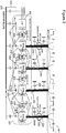
Figure 3 illustrates example EMI filtering techniques used with both transformer and capacitor based galvanic isolation circuits. The figure illustrates: an unfiltered transformer basedcommunication interface 319A; an unfiltered capacitance basedcommunication interface 319B; an EMI filtered transformer basedcommunication interface 319C; and an EMI filtered capacitance based communication interface319D. - The unfiltered transformer based
communication interface 319A comprises afirst transceiver 314A, asecond transceiver 316A and an unfiltered transformer basedgalvanic isolation circuit 318A. The unfiltered transformer basedgalvanic isolation circuit 318A comprises agalvanic isolator 334A, afirst communication link 336A, asecond communication link 338A, afirst reference terminal 320A-1 and asecond reference terminal 320A-2. - The
galvanic isolator 334A is located between thefirst transceiver 314A and thesecond transceiver 316A. Thegalvanic isolator 334A is a transformer. The first-transceiver 314A andsecond transceiver 316A may be one of the BMS transceivers or the transceiver of the CPU. Thefirst receiver 314A is connected to thefirst reference terminal 320A-1 and the second receiver is connected to thesecond reference terminal 320A-2. Thegalvanic isolator 334A is connected to thefirst transceiver 314A by thefirst communication link 336A and connected to thesecond transceiver 316A by thesecond communication link 338A. In this example, the first and second communication links are dual-line communication links that can communicate via differential signalling. - The unfiltered capacitance based
communication interface 319B comprises afirst transceiver 314B, asecond transceiver 316B and an unfiltered capacitance basedgalvanic isolation circuit 318B. The unfiltered capacitance basedgalvanic isolation circuit 318B is identical to the unfiltered transformer basedgalvanic isolation circuit 318A with the exception that thegalvanic isolator 334B comprises a pair of capacitors instead of a transformer. - The EMI filtered transformer based
communication interface 319C comprises afirst transceiver 314C, asecond transceiver 316C and an unfiltered capacitance basedgalvanic isolation circuit 318C. The EMI filtered transformer basedgalvanic isolation circuit 318C comprises the same components as described above in relation to the unfiltered transformer basedgalvanic isolation circuit 318A. In addition, the first and second communication links 336C, 338C comprise a respective first and second common mode choke (CMC) 340C, 342C. The first andsecond CMCs circuit 318C further comprises a firstcapacitive decoupling circuit 344C connected between thefirst communication link 336C and thefirst reference terminal 320C-1 and a secondcapacitive decoupling circuit 346C connected between thesecond communication link 338C and thesecond reference terminal 320C-2. Thegalvanic isolator 334C is a center-tapped transformer with two center taps. A first central terminal of the transformer is connected to thefirst reference terminal 320C-1 by a first center-tap decoupling capacitor 348. Similarly, a second central terminal of the transformer is connected to thesecond reference terminal 320C-2 by a second center-tap decoupling capacitor 350. - The EMI filtered capacitance based
communication interface 319D comprises afirst transceiver 314D, asecond transceiver 316D and an unfiltered capacitance basedgalvanic isolation circuit 318D. The EMI filtered capacitance basedgalvanic isolation circuit 318D comprises the same components as described above in relation to the unfiltered capacitance basedgalvanic isolation circuit 318B. In addition, thecircuit 318D further comprises a first andsecond CMC galvanic isolation circuit 318C. Thecircuit 318D further comprises a first split-termination circuit 352 coupled between the first communication link 336D and thefirst reference terminal 320D-1. The first split-termination circuit 352 is connected to the first communication link 336D between thefirst CMC 340D and the galvanic isolator 334D. Thecircuit 318D further comprises a second split-termination circuit 354 coupled between the second communication link 338D and thesecond reference terminal 320D-2. The second split-termination circuit 354 is connected to the second communication link 338D between thesecond CMC 342D and the galvanic isolator 334D. - The EMI filtered
circuits circuits unfiltered circuits Figures 1 and2 , can become prohibitively expensive and complex and comprise a large number of components. -
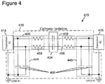
Figure 4 illustrates an example of a capacitor based communication interface 419 with high voltagetolerant transceivers tolerant transceivers galvanic isolation circuit 418, relative to the EMI filtered galvanic isolation circuits ofFigure 3 . - The reduced EMI filtered capacitance based communication interface 419 comprises a
first transceiver 414, asecond transceiver 416 and a reduced EMI filtered capacitance basedgalvanic isolation circuit 418. The reduced EMI filtered capacitance basedgalvanic isolation circuit 418 ofFigure 4 comprises the same components as described above in relation to the unfiltered capacitance basedgalvanic isolation circuit 318B ofFigure 3 . In addition, thecircuit 418 ofFigure 4 further comprises a first and secondcapacitive decoupling circuit first communication link 436 further comprises afirst resistance circuit 456 arranged between the firstcapacitive decoupling circuit 444 and thegalvanic isolator 434. Similarly, thesecond communication link 438 further comprises asecond resistance circuit 458 arranged between the secondcapacitive decoupling circuit 446 and thegalvanic isolator 434. - The first and second
capacitive decoupling circuits galvanic isolation circuit 418. The impedance ofdecoupling capacitors 460 of the first and secondcapacitive decoupling circuits - In one example, a combination of: (i)
transceivers decoupling capacitors 460 each with a capacitance of 100 pF, can satisfy a 300 mArms injected BCI current requirement at a frequency of 10 MHz. Atransceiver - If the communication interface 419 of
Figure 4 employstransceivers decoupling capacitors 460 will be required. Capacitance values higher than 100 pF can result in extra current consumption due to switching loss. Higher value decoupling capacitors can also generate a low pass filter (LPF) for any communication signal. This can limit the communication speed. - Embodiments of the present disclosure that are described below provide a circuit arrangement that can reduce EMI immunity requirements of transceivers and EMI filter circuitries. This in turn can reduce the number and cost of external components and avoid primary performance degradation of the communication interface caused by excessive filtering.
-
Figure 5 illustrates acommunication interface 519 comprising agalvanic isolation circuit 518 according to an embodiment of the present disclosure. Thegalvanic isolation circuit 518 ofFigure 5 can advantageously: (i) reduce the complexity and component requirements of EMI filter circuitry; and (ii) reduce the voltage tolerance requirements of the transceivers. - The
communication interface 519 ofFigure 5 comprises afirst transceiver 514, asecond transceiver 516 and agalvanic isolation circuit 518. Thegalvanic isolation circuit 518 comprises agalvanic isolator 534, afirst communication link 536, asecond communication link 538, a first reference terminal 520-1 and a second reference terminal 520-2. - The
galvanic isolator 534 has a first side and a second side, with each side being isolated from the other side. In this example, thegalvanic isolator 534 comprises a first isolatingcapacitor 562 and a second isolatingcapacitor 564. Thefirst communication link 536 connects the first side of thegalvanic isolator 534 to thefirst transceiver 514. Similarly, thesecond communication link 538 connects the second side of thegalvanic isolator 534 to thesecond receiver 516. In this way, the first and second transceivers can communicate with one another in a galvanically isolated manner. For example, the transceivers may belong to adjacent BMS and / or the CPU in the controller boards ofFigures 1 and2 . - The
galvanic isolation circuit 518 further comprises an ACshort capacitor 566 connected between the first reference terminal 520-1 and the second reference terminal 520-2. - The AC
short capacitor 566 provides an EMI filtering mechanism for thegalvanic isolation circuit 518. As discussed further below, the ACshort capacitor 566 can create a lower impedance path, between the first reference terminal 520-1 and the second reference terminal 520-2, in parallel to thegalvanic isolator 534. In this way, the bulk of any EMI current will flow through the ACshort capacitor 566. - The AC
short capacitor 566 is a discrete capacitor, which may be in the range of 100 pF to 100 nF. The ACshort capacitor 566 is not a parasitic capacitance. - In this example, the
galvanic isolation circuit 518 also comprises: a first capacitive decoupling circuit 544 connected between thefirst communication link 536 and the first reference terminal 520-1; and a secondcapacitive decoupling circuit 546 connected between thesecond communication link 538 and the second reference terminal 520-2. In a similar manner to the EMI filteredcircuits Figures 3 and4 , the first and secondcapacitive decoupling circuits 544, 546 can provide EMI filtering for thegalvanic isolation circuit 518. - The arrangement of the AC
short capacitor 566 between the reference terminals 520-1, 520-2 of two galvanically isolated transceivers creates a low impedance path for AC signals. This can determine a maximum magnitude of AC voltage between the reference terminals 520-1, 520-2, and in turn a magnitude of common mode AC voltage that will affect the communication interface operation for injected AC current disturbances. This relaxes the requirements of any additional EMI filter circuitry (such as the capacitive decoupling circuits 544, 546) and the voltage tolerance requirements of theinterface transceivers - In the
communication interface 519, the capacitance values ofdecoupling capacitors 560 of the first and secondcapacitive decoupling circuits 544, 546 and the voltage tolerance of the first andsecond transceivers Figure 4 . For example, the capacitance CDECOUPLING of the decoupling capacitors can be reduced or minimised enabling higher speed communication. In some embodiments, such as inFigure 6 , the decoupling capacitors can be omitted. Similarly, thegalvanic isolation circuit 518 can be used with transceivers having lower voltage tolerance than those discussed in relation to the communication interface ofFigure 4 . - The
communication interface 519 will have sufficient EMI filtering if the capacitance CAC-SHORT of the ACshort capacitor 566 is selected to satisfy the condition:

where: - CISOLATION is the capacitance of the capacitance based
galvanic isolator 534; - VCM,MAX is the voltage tolerance of the
transceivers 514, 516 (the maximum common mode voltage amplitude tolerable by transceiver design or its external protection or the maximum common mode voltage enabling faultless communication at signal transmission or reception); - IBCI is the maximum sustained current at the frequency of injection f BCI. A target BCI requirement defining a relationship between sustained IBCI and fBCI is normally described by a certain profile, current versus frequency, as a requirement of BCI testing. The profile of the target BCI requirement may have a non-linear curvature.
- In the above inequality, it is assumed that one of the capacitive decoupling circuits 544, 546 (i.e. one pair of decoupling capacitors 560) is shorted by lower impedance during a driver operation of the
corresponding transceiver - Therefore, for the
communication interface 519 comprising thegalvanic isolation circuit 518 with the ACshort capacitor 566, it is not necessary for thetransceivers decoupling capacitors 560 to have a high capacitance value. As a result, thegalvanic isolation circuit 518 can enable highspeed communication, not limited by low saturation current and / or by high parasitic capacitance of high voltage devices inside the transceiver and / or excessive external filtering. The ACshort capacitor 566 simplifies the EMI filter design for thegalvanic isolation circuit 518 and the capacitance value of the ACshort capacitor 566 can be selected using the above inequality. -
Figure 6 illustrates afurther communication interface 619 comprising agalvanic isolation circuit 618 according to an embodiment of the present disclosure. Features ofFigure 5 that are also shown inFigure 6 have been given corresponding reference numbers in the 600 series and will not necessarily be described again here. - The
galvanic isolation circuit 618 is identical to the galvanic isolation circuit ofFigure 5 , with the exception that there are no capacitive decoupling circuits. The inequalities above demonstrate that the capacitance of the capacitive decoupling circuits can become negligible when considering the performance of the galvanic isolation circuit ofFigure 5 . As a result, some embodiments of the present disclosure do not comprise a capacitive decoupling circuit. -
Figures 7 and8 compare the performance of example communication interfaces 719, 819 comprisinggalvanic isolation circuits Figure 7 illustrates the performance of acommunication interface 719 without an AC short capacitor andFigure 8 illustrates the performance of acommunication interface 819 with an ACshort capacitor 866 connected between a first reference terminal 820-1 and a second reference terminal 820-2. The figures containplots respective communication interface - The
galvanic isolation circuits Figures 7 and8 are identical with the exception of the ACshort capacitor 866. The ACshort capacitor 866 is a 5 nF capacitor. Eachgalvanic isolation circuit galvanic isolator capacitive decoupling circuits pF decoupling capacitors second transceivers - The
plots target BCI requirement plots plot 770 ofFigure 7 for thecommunication interface 719 without an AC short capacitor shows that theperformance curve 774 is below thetarget BCI requirement 772 for frequencies less than 100 MHz. In other words, thecommunication interface 719 has a minimum-EMI-filtered-frequency of 100 MHz. Therefore, thecapacitive decoupling circuits - The
plot 870 ofFigure 8 for thecommunication interface 819 comprising thegalvanic isolation circuit 818 with the ACshort capacitor 866 shows that theperformance curve 874 can meet the target BCI requirement872 for frequencies down to approximately 1 MHz. The immunity performance of thegalvanic isolation circuit 818 with the ACshort capacitor 866 demonstrates an improvement in EMI filtering performance of two orders of magnitude relative to thegalvanic isolation circuit 718 ofFigure 7 . - In this example, the 5 nF AC
short capacitor 866 is not sufficient for thecommunication interface 819 to meet the 300 mArms requirement at frequencies less than 1 MHz. In other words, thecommunication interface 819 has a minimum-EMI-filtered-frequency of 1 MHz. The value of the ACshort capacitor 866 can be increased to extend the communication interface performance to lower frequencies by lowering the minimum-EMI-filtered-frequency. However, many applications do not require this level of performance at such low frequencies. Furthermore, for various reasons, such as power limitation of a closed loop or too high impedance at low frequencies for open loop BCI injection, it can be challenging to meet the 300 mArms requirement at low frequencies. -
Figure 9 illustrates a communication interface 919 comprising a transformer basedgalvanic isolation circuit 918 according to an embodiment of the present disclosure. Features ofFigure 5 that are also shown inFigure 9 have been given corresponding reference numbers in the 900 series and will not necessarily be described again here. -
Figure 9 is identical toFigure 5 with the exception that thegalvanic isolator 934 is a transformer instead of comprising capacitors. The ACshort capacitor 966 works in the same way as described in relation toFigure 5 . The transformer basedgalvanic isolation circuit 918 can also provide sufficient EMI filtering without demanding constraints on the transceiver voltage tolerance or the decoupling capacitance. However, the transformer based solution is not as cost-effective as the capacitor based communication interfaces ofFigures 5 and 6 . Thegalvanic isolation circuit 918 ofFigure 9 includes first and second capacitive decoupling circuits 944, 946. The decoupling circuits are optional and other embodiments of the transformer based galvanic isolation circuit may operate without the decoupling circuits in a similar manner to the capacitive based circuit ofFigure 6 . - The galvanic isolation circuits disclosed in relation to
Figures 5, 6 ,8 and9 comprise dual-line communication links which can communicate via differential signalling. Referring toFigure 5 as an example, the dual line circuit is comprised as follows. Thefirst communication link 536 comprises a first-primary-link 536-1 and a first-secondary-link 536-2; and thesecond communication link 538 comprises a second-primary-link 538-1 and a second-secondary-link 538-2. In the example ofFigure 5 , the first capacitive decoupling circuit 544 comprises: a first-primary-decoupling-capacitor 560-1 connected between the first-primary-link 536-1 and the first reference terminal 520-1; and a first-secondary-decoupling-capacitor 560-2 connected between the first-secondary-link 536-2 and the first reference terminal 520-2. Similarly, the secondcapacitive decoupling circuit 546 comprises: a second-primary-decoupling-capacitor 560-3 connected between the second-primary-link 538-1 and the second reference terminal 520-2; and a second-secondary-decoupling-capacitor 560-4 connected between the second-secondary-link 538-2 and the second reference terminal 520-2. - In other example embodiments, the first and second communication links and the first and second capacitive decoupling circuits may consist of respective single links or single capacitors, in a single-line configuration.
- The use of an AC short capacitor maintains galvanic isolation between the BMS. This can be considered advantageous when compared with an alternative approach of replacing the AC short capacitor with a direct DC connection between the highest voltage of the first BMS and the reference terminal of the second BMSs, as example, using the fact that BMSs are connected to the string of battery cells in predefined order. Implementing this approach in the controller boards of
Figure 1 andFigure 2 would enable direct on the board connections of the maximum potential incoming from the battery to the reference terminals of adjacent BMS. However, connection to the battery in the wrong order would create a significant hazard that could injure a user. A different set of connectors may mitigate such risk. Nonetheless, due to the potential hazard, this approach may not be acceptable for many BMS applications. - The instructions and/or flowchart steps in the above figures can be executed in any order, unless a specific order is explicitly stated. Also, those skilled in the art will recognize that while one example set of instructions/method has been discussed, the material in this specification can be combined in a variety of ways to yield other examples as well, and are to be understood within a context provided by this detailed description.
- In some example embodiments the set of instructions/method steps described above are implemented as functional and software instructions embodied as a set of executable instructions which are effected on a computer or machine which is programmed with and controlled by said executable instructions. Such instructions are loaded for execution on a processor (such as one or more CPUs). The term processor includes microprocessors, microcontrollers, processor modules or subsystems (including one or more microprocessors or microcontrollers), or other control or computing devices. A processor can refer to a single component or to plural components.
- In other examples, the set of instructions/methods illustrated herein and data and instructions associated therewith are stored in respective storage devices, which are implemented as one or more non-transient machine or computer-readable or computer-usable storage media or mediums. Such computer-readable or computer usable storage medium or media is (are) considered to be part of an article (or article of manufacture). An article or article of manufacture can refer to any manufactured single component or multiple components. The non-transient machine or computer usable media or mediums as defined herein excludes signals, but such media or mediums may be capable of receiving and processing information from signals and/or other transient mediums.
- Example embodiments of the material discussed in this specification can be implemented in whole or in part through network, computer, or data based devices and/or services. These may include cloud, internet, intranet, mobile, desktop, processor, look-up table, microcontroller, consumer equipment, infrastructure, or other enabling devices and services. As may be used herein and in the claims, the following non-exclusive definitions are provided.
- In one example, one or more instructions or steps discussed herein are automated. The terms automated or automatically (and like variations thereof) mean controlled operation of an apparatus, system, and/or process using computers and/or mechanical/electrical devices without the necessity of human intervention, observation, effort and/or decision.
- It will be appreciated that any components said to be coupled may be coupled or connected either directly or indirectly. In the case of indirect coupling, additional components may be located between the two components that are said to be coupled.
- In this specification, example embodiments have been presented in terms of a selected set of details. However, a person of ordinary skill in the art would understand that many other example embodiments may be practiced which include a different selected set of these details. It is intended that the following claims cover all possible example embodiments.
Claims (14)
- A galvanic isolation circuit (518) comprising:a galvanic isolator (534) having a first side and a second side;a first communication link (536) connected to the first side of the galvanic isolator and connectable to a first transceiver (514);a second communication link (538) connected to the second side of the galvanic isolator and connectable to a second transceiver (516);a first reference terminal (520-1) connectable to the first transceiver (514);a second reference terminal (520-2) connectable to the second transceiver (516); andan AC short capacitor (566) connected between the first reference terminal (520-1) and the second reference terminal (520-2).
- The galvanic isolation circuit (518) of claim 1, wherein the AC short capacitor (566) is a discrete capacitor.
- The galvanic isolation circuit (518) of claim 1 or claim 2 further comprising:a first capacitive decoupling circuit (544) connected between the first communication link (536) and the first reference terminal (520-1); anda second capacitive decoupling circuit (546) connected between the second communication link (538) and the second reference terminal (520-2).
- The galvanic isolation circuit (518) of claim 3, wherein:the first communication link (536) comprises a first-primary-link (536-1) and a first-secondary-link (536-2); andthe second communication link (538) comprises a second-primary-link (538-1) and a second-secondary-link (538-2);the first capacitive decoupling circuit (544) comprises:a first-primary-decoupling-capacitor (560-1) connected between the first-primary-link (536-1) and the first reference terminal (520-1); anda first-secondary-decoupling-capacitor (560-2) connected between the first-secondary-link (536-2) and the first reference terminal (520-1); andthe second capacitive decoupling circuit (546) comprises:a second-primary-decoupling-capacitor (560-3) connected between the second-primary-link (538-1) and the second reference terminal (520-2); anda second-secondary-decoupling-capacitor (560-4) connected between the second-secondary-link (538-2) and the second reference terminal (520-2).
- The galvanic isolation circuit (518) of any preceding claim, wherein the galvanic isolator comprises a capacitive galvanic isolator.
- The galvanic isolation circuit (518) of claim 4, wherein the capacitive galvanic isolator comprises:a primary capacitor (562) connected between the first-primary-link (536-1) and the second-primary-link (538-1); anda secondary capacitor (564) connected between the first-secondary-link (536-2) and the second-secondary-link (538-2).
- The galvanic isolation circuit (918) of any of claims 1 to 3, wherein the galvanic isolator (934) comprises a transformer.
- The galvanic isolation circuit (518) of any preceding claim, wherein the galvanic isolation circuit has a transceiver-voltage-tolerance-rating and a target BCI requirement defining a sustained current versus frequency relationship, and wherein a capacitance value of the AC short capacitor (566) is selected based on the transceiver-voltage-tolerance-rating and the target BCI requirement.
- The galvanic isolation circuit (518) of any preceding claim, wherein the AC short capacitor (566) is a discrete capacitor with a capacitance greater than or equal to 100 pF.
- A communication interface (519) comprising:a first transceiver (514);a second transceiver (516); andthe galvanic isolation circuit (518) of any preceding claim.
- The communication interface (519) of claim 10, wherein the communication interface has a target BCI requirement defining sustained current versus injection frequency and wherein a capacitance value of the AC short capacitor (566) is selected based on:a voltage tolerance of the first transceiver (514);a voltage tolerance of the second transceiver (516); andthe target BCI requirement.
- A battery management control circuit comprising a plurality of the galvanic isolation circuits (518) of any of claims 1 to 9.
- The battery management control circuit of claim 12 further comprising:a processor (106) comprising a transceiver (121); anda plurality of battery management systems (108), each comprising a first transceiver (114) and a second transceiver (116);wherein each of the plurality of galvanic isolation circuits (118) connect adjacent ones of the battery management systems (108) and the processor (106).
- The battery management control circuit of claim 13, wherein a first transceiver (514) of one battery management system, a second transceiver (516) of an adjacent battery management system and one galvanic isolation circuit (518) form an EMI-filtered galvanically isolated communication interface (519).
Priority Applications (3)
| Application Number | Priority Date | Filing Date | Title |
|---|---|---|---|
| EP19166177.6A EP3716554B1 (en) | 2019-03-29 | 2019-03-29 | Galvanic isolation circuit |
| US16/802,862 US11063789B2 (en) | 2019-03-29 | 2020-02-27 | Galvanic isolation circuit |
| CN202010184591.8A CN111756349B (en) | 2019-03-29 | 2020-03-16 | Electrical isolation circuit |
Applications Claiming Priority (1)
| Application Number | Priority Date | Filing Date | Title |
|---|---|---|---|
| EP19166177.6A EP3716554B1 (en) | 2019-03-29 | 2019-03-29 | Galvanic isolation circuit |
Publications (2)
| Publication Number | Publication Date |
|---|---|
| EP3716554A1 true EP3716554A1 (en) | 2020-09-30 |
| EP3716554B1 EP3716554B1 (en) | 2024-03-13 |
Family
ID=66217694
Family Applications (1)
| Application Number | Title | Priority Date | Filing Date |
|---|---|---|---|
| EP19166177.6A Active EP3716554B1 (en) | 2019-03-29 | 2019-03-29 | Galvanic isolation circuit |
Country Status (3)
| Country | Link |
|---|---|
| US (1) | US11063789B2 (en) |
| EP (1) | EP3716554B1 (en) |
| CN (1) | CN111756349B (en) |
Cited By (1)
| Publication number | Priority date | Publication date | Assignee | Title |
|---|---|---|---|---|
| WO2025031773A1 (en) * | 2023-08-04 | 2025-02-13 | Robert Bosch Gmbh | Structural unit for a battery management system |
Families Citing this family (5)
| Publication number | Priority date | Publication date | Assignee | Title |
|---|---|---|---|---|
| JP7558028B2 (en) * | 2020-10-21 | 2024-09-30 | 日立Astemo株式会社 | Battery Control Unit |
| EP4239346B1 (en) | 2022-01-07 | 2025-01-01 | Contemporary Amperex Technology (Hong Kong) Limited | Cell sampling circuit, circuit fault early-warning method, and battery management system |
| CN115825794B (en) * | 2022-01-07 | 2023-11-17 | 宁德时代新能源科技股份有限公司 | Battery core sampling circuit, circuit fault early warning method and battery management system |
| EP4617106A1 (en) * | 2024-03-11 | 2025-09-17 | Volvo Penta Corporation | A communications interface, a communications system and a marine vessel |
| EP4632994A1 (en) * | 2024-04-11 | 2025-10-15 | Instagrid GmbH | Systems and methods for management of an energy unit |
Citations (4)
| Publication number | Priority date | Publication date | Assignee | Title |
|---|---|---|---|---|
| US6023202A (en) * | 1998-02-13 | 2000-02-08 | Hewlett-Packard Company | Ground return for high speed digital signals that are capacitively coupled across a DC-isolated interface |
| EP1168804A2 (en) * | 2000-06-28 | 2002-01-02 | Agere Systems Guardian Corporation | Inductive coupling for silicon data access arrangement |
| US20060055379A1 (en) * | 2004-09-14 | 2006-03-16 | Denso Corporation | Semiconductor integrated circuit |
| US20100284452A1 (en) * | 2009-05-08 | 2010-11-11 | Intersil Americas Inc. | Capacitive divider transmission scheme for improved communications isolation |
Family Cites Families (8)
| Publication number | Priority date | Publication date | Assignee | Title |
|---|---|---|---|---|
| US5615091A (en) * | 1995-10-11 | 1997-03-25 | Biochem International, Inc. | Isolation transformer for medical equipment |
| CN1183587C (en) * | 1996-04-08 | 2005-01-05 | 德克萨斯仪器股份有限公司 | Method and apparatus for galvanically isolating two integrated circuits from each others |
| US5870046A (en) * | 1997-04-22 | 1999-02-09 | Silicon Laboratories Inc. | Analog isolation system with digital communication across a capacitive barrier |
| US8049573B2 (en) * | 2004-06-03 | 2011-11-01 | Silicon Laboratories Inc. | Bidirectional multiplexed RF isolator |
| US8380905B2 (en) * | 2010-05-21 | 2013-02-19 | National Semiconductor Corporation | Isolated communication bus and related protocol |
| CN102064356B (en) * | 2010-12-21 | 2012-09-19 | 深圳市佳华利道新技术开发有限公司 | Battery management system |
| JP2018501758A (en) * | 2014-12-09 | 2018-01-18 | ジョンソン コントロールズ テクノロジー カンパニーJohnson Controls Technology Company | Electromagnetic compatibility filter |
| US9473329B1 (en) * | 2015-01-21 | 2016-10-18 | Holt Integrated Circuits | Analog front-end with galvanically isolated differential bus |
-
2019
- 2019-03-29 EP EP19166177.6A patent/EP3716554B1/en active Active
-
2020
- 2020-02-27 US US16/802,862 patent/US11063789B2/en active Active
- 2020-03-16 CN CN202010184591.8A patent/CN111756349B/en active Active
Patent Citations (4)
| Publication number | Priority date | Publication date | Assignee | Title |
|---|---|---|---|---|
| US6023202A (en) * | 1998-02-13 | 2000-02-08 | Hewlett-Packard Company | Ground return for high speed digital signals that are capacitively coupled across a DC-isolated interface |
| EP1168804A2 (en) * | 2000-06-28 | 2002-01-02 | Agere Systems Guardian Corporation | Inductive coupling for silicon data access arrangement |
| US20060055379A1 (en) * | 2004-09-14 | 2006-03-16 | Denso Corporation | Semiconductor integrated circuit |
| US20100284452A1 (en) * | 2009-05-08 | 2010-11-11 | Intersil Americas Inc. | Capacitive divider transmission scheme for improved communications isolation |
Non-Patent Citations (1)
| Title |
|---|
| LORENTZ V R H ET AL: "Novel cost-efficient contactless distributed monitoring concept for smart battery cells", INDUSTRIAL ELECTRONICS (ISIE), 2012 IEEE INTERNATIONAL SYMPOSIUM ON, IEEE, 28 May 2012 (2012-05-28), pages 1342 - 1347, XP032199907, ISBN: 978-1-4673-0159-6, DOI: 10.1109/ISIE.2012.6237285 * |
Cited By (1)
| Publication number | Priority date | Publication date | Assignee | Title |
|---|---|---|---|---|
| WO2025031773A1 (en) * | 2023-08-04 | 2025-02-13 | Robert Bosch Gmbh | Structural unit for a battery management system |
Also Published As
| Publication number | Publication date |
|---|---|
| EP3716554B1 (en) | 2024-03-13 |
| US20200313934A1 (en) | 2020-10-01 |
| CN111756349A (en) | 2020-10-09 |
| US11063789B2 (en) | 2021-07-13 |
| CN111756349B (en) | 2025-07-08 |
Similar Documents
| Publication | Publication Date | Title |
|---|---|---|
| EP3716554B1 (en) | Galvanic isolation circuit | |
| US11870366B2 (en) | System and method for power converter interfacing with multiple series-stacked voltage domains | |
| US10700544B2 (en) | Wireless power transmission device and system using impedance matching | |
| EP4075656B1 (en) | Charging systems with direct charging port support and extended capabilities | |
| Sinha et al. | Design of efficient matching networks for capacitive wireless power transfer systems | |
| Su et al. | Full-duplex communication on the shared channel of a capacitively coupled power transfer system | |
| CN108172912A (en) | Electricity core sampling circuit | |
| KR20130135055A (en) | Storage device system and communication method of storage device system | |
| EP3338339B1 (en) | Methods and circuits configured to provide for multi-phase wireless power transfer | |
| EP4218115A1 (en) | Wireless charging pad for power tool battery packs | |
| CN108616168A (en) | The wireless charging system electromagnetic interference prediction circuit of mode of resonance containing repeating coil and method | |
| US20170040796A1 (en) | Communication system in an electrical facility including batteries | |
| JPWO2019073757A1 (en) | Battery system | |
| US20140044998A1 (en) | High voltage battery system for a vehicle | |
| CN107636979A (en) | Power/data electric coupler | |
| US20190319463A1 (en) | Energy balancing circuit and energy balancing apparatus | |
| AU2020345857B2 (en) | Electrical power regulating apparatus | |
| CN109302067A (en) | Single Stage DC-DC Power Converter | |
| EP3795411B1 (en) | Storage battery monitoring system, battery pack, and electric vehicle | |
| EP3316389A1 (en) | Battery system, communication circuit for a battery system and vehicle | |
| US12463456B2 (en) | Portable power supply with bidirectional charging and passthrough | |
| Sun et al. | Detecting load resistance and mutual inductance in series‐parallel compensated wireless power transfer system based on input‐side measurement | |
| Wang et al. | Flexible design method for multiple loads inductive power transfer system with equal power distribution | |
| CN114465615A (en) | Radiation processing system of server management net gape | |
| EP4723497A1 (en) | An antenna arrangement |
Legal Events
| Date | Code | Title | Description |
|---|---|---|---|
| PUAI | Public reference made under article 153(3) epc to a published international application that has entered the european phase |
Free format text: ORIGINAL CODE: 0009012 |
|
| STAA | Information on the status of an ep patent application or granted ep patent |
Free format text: STATUS: THE APPLICATION HAS BEEN PUBLISHED |
|
| AK | Designated contracting states |
Kind code of ref document: A1 Designated state(s): AL AT BE BG CH CY CZ DE DK EE ES FI FR GB GR HR HU IE IS IT LI LT LU LV MC MK MT NL NO PL PT RO RS SE SI SK SM TR |
|
| AX | Request for extension of the european patent |
Extension state: BA ME |
|
| STAA | Information on the status of an ep patent application or granted ep patent |
Free format text: STATUS: REQUEST FOR EXAMINATION WAS MADE |
|
| 17P | Request for examination filed |
Effective date: 20210330 |
|
| RBV | Designated contracting states (corrected) |
Designated state(s): AL AT BE BG CH CY CZ DE DK EE ES FI FR GB GR HR HU IE IS IT LI LT LU LV MC MK MT NL NO PL PT RO RS SE SI SK SM TR |
|
| STAA | Information on the status of an ep patent application or granted ep patent |
Free format text: STATUS: EXAMINATION IS IN PROGRESS |
|
| 17Q | First examination report despatched |
Effective date: 20220429 |
|
| GRAP | Despatch of communication of intention to grant a patent |
Free format text: ORIGINAL CODE: EPIDOSNIGR1 |
|
| STAA | Information on the status of an ep patent application or granted ep patent |
Free format text: STATUS: GRANT OF PATENT IS INTENDED |
|
| INTG | Intention to grant announced |
Effective date: 20231208 |
|
| GRAS | Grant fee paid |
Free format text: ORIGINAL CODE: EPIDOSNIGR3 |
|
| GRAA | (expected) grant |
Free format text: ORIGINAL CODE: 0009210 |
|
| STAA | Information on the status of an ep patent application or granted ep patent |
Free format text: STATUS: THE PATENT HAS BEEN GRANTED |
|
| AK | Designated contracting states |
Kind code of ref document: B1 Designated state(s): AL AT BE BG CH CY CZ DE DK EE ES FI FR GB GR HR HU IE IS IT LI LT LU LV MC MK MT NL NO PL PT RO RS SE SI SK SM TR |
|
| REG | Reference to a national code |
Ref country code: GB Ref legal event code: FG4D |
|
| REG | Reference to a national code |
Ref country code: CH Ref legal event code: EP |
|
| REG | Reference to a national code |
Ref country code: DE Ref legal event code: R096 Ref document number: 602019048093 Country of ref document: DE |
|
| REG | Reference to a national code |
Ref country code: IE Ref legal event code: FG4D |
|
| PGFP | Annual fee paid to national office [announced via postgrant information from national office to epo] |
Ref country code: GB Payment date: 20240419 Year of fee payment: 6 |
|
| PG25 | Lapsed in a contracting state [announced via postgrant information from national office to epo] |
Ref country code: LT Free format text: LAPSE BECAUSE OF FAILURE TO SUBMIT A TRANSLATION OF THE DESCRIPTION OR TO PAY THE FEE WITHIN THE PRESCRIBED TIME-LIMIT Effective date: 20240313 |
|
| REG | Reference to a national code |
Ref country code: LT Ref legal event code: MG9D |
|
| PG25 | Lapsed in a contracting state [announced via postgrant information from national office to epo] |
Ref country code: GR Free format text: LAPSE BECAUSE OF FAILURE TO SUBMIT A TRANSLATION OF THE DESCRIPTION OR TO PAY THE FEE WITHIN THE PRESCRIBED TIME-LIMIT Effective date: 20240614 |
|
| REG | Reference to a national code |
Ref country code: NL Ref legal event code: MP Effective date: 20240313 |
|
| PG25 | Lapsed in a contracting state [announced via postgrant information from national office to epo] |
Ref country code: RS Free format text: LAPSE BECAUSE OF FAILURE TO SUBMIT A TRANSLATION OF THE DESCRIPTION OR TO PAY THE FEE WITHIN THE PRESCRIBED TIME-LIMIT Effective date: 20240613 Ref country code: HR Free format text: LAPSE BECAUSE OF FAILURE TO SUBMIT A TRANSLATION OF THE DESCRIPTION OR TO PAY THE FEE WITHIN THE PRESCRIBED TIME-LIMIT Effective date: 20240313 |
|
| PG25 | Lapsed in a contracting state [announced via postgrant information from national office to epo] |
Ref country code: ES Free format text: LAPSE BECAUSE OF FAILURE TO SUBMIT A TRANSLATION OF THE DESCRIPTION OR TO PAY THE FEE WITHIN THE PRESCRIBED TIME-LIMIT Effective date: 20240313 |
|
| PG25 | Lapsed in a contracting state [announced via postgrant information from national office to epo] |
Ref country code: RS Free format text: LAPSE BECAUSE OF FAILURE TO SUBMIT A TRANSLATION OF THE DESCRIPTION OR TO PAY THE FEE WITHIN THE PRESCRIBED TIME-LIMIT Effective date: 20240613 Ref country code: NO Free format text: LAPSE BECAUSE OF FAILURE TO SUBMIT A TRANSLATION OF THE DESCRIPTION OR TO PAY THE FEE WITHIN THE PRESCRIBED TIME-LIMIT Effective date: 20240613 Ref country code: LT Free format text: LAPSE BECAUSE OF FAILURE TO SUBMIT A TRANSLATION OF THE DESCRIPTION OR TO PAY THE FEE WITHIN THE PRESCRIBED TIME-LIMIT Effective date: 20240313 Ref country code: HR Free format text: LAPSE BECAUSE OF FAILURE TO SUBMIT A TRANSLATION OF THE DESCRIPTION OR TO PAY THE FEE WITHIN THE PRESCRIBED TIME-LIMIT Effective date: 20240313 Ref country code: GR Free format text: LAPSE BECAUSE OF FAILURE TO SUBMIT A TRANSLATION OF THE DESCRIPTION OR TO PAY THE FEE WITHIN THE PRESCRIBED TIME-LIMIT Effective date: 20240614 Ref country code: FI Free format text: LAPSE BECAUSE OF FAILURE TO SUBMIT A TRANSLATION OF THE DESCRIPTION OR TO PAY THE FEE WITHIN THE PRESCRIBED TIME-LIMIT Effective date: 20240313 Ref country code: ES Free format text: LAPSE BECAUSE OF FAILURE TO SUBMIT A TRANSLATION OF THE DESCRIPTION OR TO PAY THE FEE WITHIN THE PRESCRIBED TIME-LIMIT Effective date: 20240313 Ref country code: BG Free format text: LAPSE BECAUSE OF FAILURE TO SUBMIT A TRANSLATION OF THE DESCRIPTION OR TO PAY THE FEE WITHIN THE PRESCRIBED TIME-LIMIT Effective date: 20240313 |
|
| REG | Reference to a national code |
Ref country code: AT Ref legal event code: MK05 Ref document number: 1666784 Country of ref document: AT Kind code of ref document: T Effective date: 20240313 |
|
| PG25 | Lapsed in a contracting state [announced via postgrant information from national office to epo] |
Ref country code: SE Free format text: LAPSE BECAUSE OF FAILURE TO SUBMIT A TRANSLATION OF THE DESCRIPTION OR TO PAY THE FEE WITHIN THE PRESCRIBED TIME-LIMIT Effective date: 20240313 Ref country code: LV Free format text: LAPSE BECAUSE OF FAILURE TO SUBMIT A TRANSLATION OF THE DESCRIPTION OR TO PAY THE FEE WITHIN THE PRESCRIBED TIME-LIMIT Effective date: 20240313 |
|
| PG25 | Lapsed in a contracting state [announced via postgrant information from national office to epo] |
Ref country code: NL Free format text: LAPSE BECAUSE OF FAILURE TO SUBMIT A TRANSLATION OF THE DESCRIPTION OR TO PAY THE FEE WITHIN THE PRESCRIBED TIME-LIMIT Effective date: 20240313 |
|
| PG25 | Lapsed in a contracting state [announced via postgrant information from national office to epo] |
Ref country code: NL Free format text: LAPSE BECAUSE OF FAILURE TO SUBMIT A TRANSLATION OF THE DESCRIPTION OR TO PAY THE FEE WITHIN THE PRESCRIBED TIME-LIMIT Effective date: 20240313 |
|
| PG25 | Lapsed in a contracting state [announced via postgrant information from national office to epo] |
Ref country code: IS Free format text: LAPSE BECAUSE OF FAILURE TO SUBMIT A TRANSLATION OF THE DESCRIPTION OR TO PAY THE FEE WITHIN THE PRESCRIBED TIME-LIMIT Effective date: 20240713 |
|
| PG25 | Lapsed in a contracting state [announced via postgrant information from national office to epo] |
Ref country code: PT Free format text: LAPSE BECAUSE OF FAILURE TO SUBMIT A TRANSLATION OF THE DESCRIPTION OR TO PAY THE FEE WITHIN THE PRESCRIBED TIME-LIMIT Effective date: 20240715 Ref country code: SM Free format text: LAPSE BECAUSE OF FAILURE TO SUBMIT A TRANSLATION OF THE DESCRIPTION OR TO PAY THE FEE WITHIN THE PRESCRIBED TIME-LIMIT Effective date: 20240313 |
|
| PG25 | Lapsed in a contracting state [announced via postgrant information from national office to epo] |
Ref country code: CZ Free format text: LAPSE BECAUSE OF FAILURE TO SUBMIT A TRANSLATION OF THE DESCRIPTION OR TO PAY THE FEE WITHIN THE PRESCRIBED TIME-LIMIT Effective date: 20240313 Ref country code: EE Free format text: LAPSE BECAUSE OF FAILURE TO SUBMIT A TRANSLATION OF THE DESCRIPTION OR TO PAY THE FEE WITHIN THE PRESCRIBED TIME-LIMIT Effective date: 20240313 |
|
| PG25 | Lapsed in a contracting state [announced via postgrant information from national office to epo] |
Ref country code: AT Free format text: LAPSE BECAUSE OF FAILURE TO SUBMIT A TRANSLATION OF THE DESCRIPTION OR TO PAY THE FEE WITHIN THE PRESCRIBED TIME-LIMIT Effective date: 20240313 |
|
| PG25 | Lapsed in a contracting state [announced via postgrant information from national office to epo] |
Ref country code: PL Free format text: LAPSE BECAUSE OF FAILURE TO SUBMIT A TRANSLATION OF THE DESCRIPTION OR TO PAY THE FEE WITHIN THE PRESCRIBED TIME-LIMIT Effective date: 20240313 |
|
| PG25 | Lapsed in a contracting state [announced via postgrant information from national office to epo] |
Ref country code: SK Free format text: LAPSE BECAUSE OF FAILURE TO SUBMIT A TRANSLATION OF THE DESCRIPTION OR TO PAY THE FEE WITHIN THE PRESCRIBED TIME-LIMIT Effective date: 20240313 |
|
| PG25 | Lapsed in a contracting state [announced via postgrant information from national office to epo] |
Ref country code: SM Free format text: LAPSE BECAUSE OF FAILURE TO SUBMIT A TRANSLATION OF THE DESCRIPTION OR TO PAY THE FEE WITHIN THE PRESCRIBED TIME-LIMIT Effective date: 20240313 Ref country code: SK Free format text: LAPSE BECAUSE OF FAILURE TO SUBMIT A TRANSLATION OF THE DESCRIPTION OR TO PAY THE FEE WITHIN THE PRESCRIBED TIME-LIMIT Effective date: 20240313 Ref country code: RO Free format text: LAPSE BECAUSE OF FAILURE TO SUBMIT A TRANSLATION OF THE DESCRIPTION OR TO PAY THE FEE WITHIN THE PRESCRIBED TIME-LIMIT Effective date: 20240313 Ref country code: PT Free format text: LAPSE BECAUSE OF FAILURE TO SUBMIT A TRANSLATION OF THE DESCRIPTION OR TO PAY THE FEE WITHIN THE PRESCRIBED TIME-LIMIT Effective date: 20240715 Ref country code: PL Free format text: LAPSE BECAUSE OF FAILURE TO SUBMIT A TRANSLATION OF THE DESCRIPTION OR TO PAY THE FEE WITHIN THE PRESCRIBED TIME-LIMIT Effective date: 20240313 Ref country code: IS Free format text: LAPSE BECAUSE OF FAILURE TO SUBMIT A TRANSLATION OF THE DESCRIPTION OR TO PAY THE FEE WITHIN THE PRESCRIBED TIME-LIMIT Effective date: 20240713 Ref country code: EE Free format text: LAPSE BECAUSE OF FAILURE TO SUBMIT A TRANSLATION OF THE DESCRIPTION OR TO PAY THE FEE WITHIN THE PRESCRIBED TIME-LIMIT Effective date: 20240313 Ref country code: CZ Free format text: LAPSE BECAUSE OF FAILURE TO SUBMIT A TRANSLATION OF THE DESCRIPTION OR TO PAY THE FEE WITHIN THE PRESCRIBED TIME-LIMIT Effective date: 20240313 Ref country code: AT Free format text: LAPSE BECAUSE OF FAILURE TO SUBMIT A TRANSLATION OF THE DESCRIPTION OR TO PAY THE FEE WITHIN THE PRESCRIBED TIME-LIMIT Effective date: 20240313 |
|
| REG | Reference to a national code |
Ref country code: CH Ref legal event code: PL |
|
| PG25 | Lapsed in a contracting state [announced via postgrant information from national office to epo] |
Ref country code: LU Free format text: LAPSE BECAUSE OF NON-PAYMENT OF DUE FEES Effective date: 20240329 |
|
| PG25 | Lapsed in a contracting state [announced via postgrant information from national office to epo] |
Ref country code: LU Free format text: LAPSE BECAUSE OF NON-PAYMENT OF DUE FEES Effective date: 20240329 |
|
| PG25 | Lapsed in a contracting state [announced via postgrant information from national office to epo] |
Ref country code: IT Free format text: LAPSE BECAUSE OF FAILURE TO SUBMIT A TRANSLATION OF THE DESCRIPTION OR TO PAY THE FEE WITHIN THE PRESCRIBED TIME-LIMIT Effective date: 20240313 |
|
| REG | Reference to a national code |
Ref country code: DE Ref legal event code: R097 Ref document number: 602019048093 Country of ref document: DE Ref country code: BE Ref legal event code: MM Effective date: 20240331 |
|
| PG25 | Lapsed in a contracting state [announced via postgrant information from national office to epo] |
Ref country code: IT Free format text: LAPSE BECAUSE OF FAILURE TO SUBMIT A TRANSLATION OF THE DESCRIPTION OR TO PAY THE FEE WITHIN THE PRESCRIBED TIME-LIMIT Effective date: 20240313 |
|
| PG25 | Lapsed in a contracting state [announced via postgrant information from national office to epo] |
Ref country code: MC Free format text: LAPSE BECAUSE OF FAILURE TO SUBMIT A TRANSLATION OF THE DESCRIPTION OR TO PAY THE FEE WITHIN THE PRESCRIBED TIME-LIMIT Effective date: 20240313 |
|
| PG25 | Lapsed in a contracting state [announced via postgrant information from national office to epo] |
Ref country code: DK Free format text: LAPSE BECAUSE OF FAILURE TO SUBMIT A TRANSLATION OF THE DESCRIPTION OR TO PAY THE FEE WITHIN THE PRESCRIBED TIME-LIMIT Effective date: 20240313 |
|
| PG25 | Lapsed in a contracting state [announced via postgrant information from national office to epo] |
Ref country code: BE Free format text: LAPSE BECAUSE OF NON-PAYMENT OF DUE FEES Effective date: 20240331 |
|
| PLBE | No opposition filed within time limit |
Free format text: ORIGINAL CODE: 0009261 |
|
| STAA | Information on the status of an ep patent application or granted ep patent |
Free format text: STATUS: NO OPPOSITION FILED WITHIN TIME LIMIT |
|
| PG25 | Lapsed in a contracting state [announced via postgrant information from national office to epo] |
Ref country code: IE Free format text: LAPSE BECAUSE OF NON-PAYMENT OF DUE FEES Effective date: 20240329 |
|
| PG25 | Lapsed in a contracting state [announced via postgrant information from national office to epo] |
Ref country code: MC Free format text: LAPSE BECAUSE OF FAILURE TO SUBMIT A TRANSLATION OF THE DESCRIPTION OR TO PAY THE FEE WITHIN THE PRESCRIBED TIME-LIMIT Effective date: 20240313 Ref country code: IE Free format text: LAPSE BECAUSE OF NON-PAYMENT OF DUE FEES Effective date: 20240329 Ref country code: DK Free format text: LAPSE BECAUSE OF FAILURE TO SUBMIT A TRANSLATION OF THE DESCRIPTION OR TO PAY THE FEE WITHIN THE PRESCRIBED TIME-LIMIT Effective date: 20240313 Ref country code: BE Free format text: LAPSE BECAUSE OF NON-PAYMENT OF DUE FEES Effective date: 20240331 Ref country code: CH Free format text: LAPSE BECAUSE OF NON-PAYMENT OF DUE FEES Effective date: 20240331 |
|
| 26N | No opposition filed |
Effective date: 20241216 |
|
| PG25 | Lapsed in a contracting state [announced via postgrant information from national office to epo] |
Ref country code: SI Free format text: LAPSE BECAUSE OF FAILURE TO SUBMIT A TRANSLATION OF THE DESCRIPTION OR TO PAY THE FEE WITHIN THE PRESCRIBED TIME-LIMIT Effective date: 20240313 |
|
| PG25 | Lapsed in a contracting state [announced via postgrant information from national office to epo] |
Ref country code: FR Free format text: LAPSE BECAUSE OF NON-PAYMENT OF DUE FEES Effective date: 20240513 |
|
| P01 | Opt-out of the competence of the unified patent court (upc) registered |
Free format text: CASE NUMBER: APP_29857/2025 Effective date: 20250623 |
|
| PG25 | Lapsed in a contracting state [announced via postgrant information from national office to epo] |
Ref country code: CY Free format text: LAPSE BECAUSE OF FAILURE TO SUBMIT A TRANSLATION OF THE DESCRIPTION OR TO PAY THE FEE WITHIN THE PRESCRIBED TIME-LIMIT; INVALID AB INITIO Effective date: 20190329 |
|
| PG25 | Lapsed in a contracting state [announced via postgrant information from national office to epo] |
Ref country code: HU Free format text: LAPSE BECAUSE OF FAILURE TO SUBMIT A TRANSLATION OF THE DESCRIPTION OR TO PAY THE FEE WITHIN THE PRESCRIBED TIME-LIMIT; INVALID AB INITIO Effective date: 20190329 |
|
| GBPC | Gb: european patent ceased through non-payment of renewal fee |
Effective date: 20250329 |
|
| PG25 | Lapsed in a contracting state [announced via postgrant information from national office to epo] |
Ref country code: TR Free format text: LAPSE BECAUSE OF FAILURE TO SUBMIT A TRANSLATION OF THE DESCRIPTION OR TO PAY THE FEE WITHIN THE PRESCRIBED TIME-LIMIT Effective date: 20240313 |
|
| PG25 | Lapsed in a contracting state [announced via postgrant information from national office to epo] |
Ref country code: GB Free format text: LAPSE BECAUSE OF NON-PAYMENT OF DUE FEES Effective date: 20250329 |
|
| PGFP | Annual fee paid to national office [announced via postgrant information from national office to epo] |
Ref country code: DE Payment date: 20260219 Year of fee payment: 8 |