EP3716463A1 - Current reduction device - Google Patents
Current reduction device Download PDFInfo
- Publication number
- EP3716463A1 EP3716463A1 EP18881549.2A EP18881549A EP3716463A1 EP 3716463 A1 EP3716463 A1 EP 3716463A1 EP 18881549 A EP18881549 A EP 18881549A EP 3716463 A1 EP3716463 A1 EP 3716463A1
- Authority
- EP
- European Patent Office
- Prior art keywords
- switching device
- bus bar
- current
- resister
- wire
- Prior art date
- Legal status (The legal status is an assumption and is not a legal conclusion. Google has not performed a legal analysis and makes no representation as to the accuracy of the status listed.)
- Granted
Links
Images



Classifications
-
- H—ELECTRICITY
- H02—GENERATION; CONVERSION OR DISTRIBUTION OF ELECTRIC POWER
- H02M—APPARATUS FOR CONVERSION BETWEEN AC AND AC, BETWEEN AC AND DC, OR BETWEEN DC AND DC, AND FOR USE WITH MAINS OR SIMILAR POWER SUPPLY SYSTEMS; CONVERSION OF DC OR AC INPUT POWER INTO SURGE OUTPUT POWER; CONTROL OR REGULATION THEREOF
- H02M1/00—Details of apparatus for conversion
- H02M1/36—Means for starting or stopping converters
-
- B—PERFORMING OPERATIONS; TRANSPORTING
- B60—VEHICLES IN GENERAL
- B60L—PROPULSION OF ELECTRICALLY-PROPELLED VEHICLES; SUPPLYING ELECTRIC POWER FOR AUXILIARY EQUIPMENT OF ELECTRICALLY-PROPELLED VEHICLES; ELECTRODYNAMIC BRAKE SYSTEMS FOR VEHICLES IN GENERAL; MAGNETIC SUSPENSION OR LEVITATION FOR VEHICLES; MONITORING OPERATING VARIABLES OF ELECTRICALLY-PROPELLED VEHICLES; ELECTRIC SAFETY DEVICES FOR ELECTRICALLY-PROPELLED VEHICLES
- B60L3/00—Electric devices on electrically-propelled vehicles for safety purposes; Monitoring operating variables, e.g. speed, deceleration or energy consumption
- B60L3/04—Cutting off the power supply under fault conditions
-
- B—PERFORMING OPERATIONS; TRANSPORTING
- B60—VEHICLES IN GENERAL
- B60L—PROPULSION OF ELECTRICALLY-PROPELLED VEHICLES; SUPPLYING ELECTRIC POWER FOR AUXILIARY EQUIPMENT OF ELECTRICALLY-PROPELLED VEHICLES; ELECTRODYNAMIC BRAKE SYSTEMS FOR VEHICLES IN GENERAL; MAGNETIC SUSPENSION OR LEVITATION FOR VEHICLES; MONITORING OPERATING VARIABLES OF ELECTRICALLY-PROPELLED VEHICLES; ELECTRIC SAFETY DEVICES FOR ELECTRICALLY-PROPELLED VEHICLES
- B60L9/00—Electric propulsion with power supply external to the vehicle
- B60L9/16—Electric propulsion with power supply external to the vehicle using AC induction motors
- B60L9/18—Electric propulsion with power supply external to the vehicle using AC induction motors fed from DC supply lines
-
- H—ELECTRICITY
- H02—GENERATION; CONVERSION OR DISTRIBUTION OF ELECTRIC POWER
- H02M—APPARATUS FOR CONVERSION BETWEEN AC AND AC, BETWEEN AC AND DC, OR BETWEEN DC AND DC, AND FOR USE WITH MAINS OR SIMILAR POWER SUPPLY SYSTEMS; CONVERSION OF DC OR AC INPUT POWER INTO SURGE OUTPUT POWER; CONTROL OR REGULATION THEREOF
- H02M7/00—Conversion of AC power input into DC power output; Conversion of DC power input into AC power output
- H02M7/003—Constructional details, e.g. physical layout, assembly, wiring or busbar connections
-
- B—PERFORMING OPERATIONS; TRANSPORTING
- B60—VEHICLES IN GENERAL
- B60L—PROPULSION OF ELECTRICALLY-PROPELLED VEHICLES; SUPPLYING ELECTRIC POWER FOR AUXILIARY EQUIPMENT OF ELECTRICALLY-PROPELLED VEHICLES; ELECTRODYNAMIC BRAKE SYSTEMS FOR VEHICLES IN GENERAL; MAGNETIC SUSPENSION OR LEVITATION FOR VEHICLES; MONITORING OPERATING VARIABLES OF ELECTRICALLY-PROPELLED VEHICLES; ELECTRIC SAFETY DEVICES FOR ELECTRICALLY-PROPELLED VEHICLES
- B60L2270/00—Problem solutions or means not otherwise provided for
- B60L2270/20—Inrush current reduction, i.e. avoiding high currents when connecting the battery
Definitions
- the present invention relates to a current reduction device that is disposed between a line breaker and a power converter.
- a power converter and a filter reactor which are driving electric devices, and further a signaling device, are installed.
- monitoring devices that grasp the degradation and failures of rail car devices or facilities. Since the underfloor space of the railway vehicle has limitations, in order to newly install these monitoring devices on the rail car, it is necessary to reduce the sizes of driving electric devices.
- an IGBT Insulated Gate Bipolar Transistor
- MOSFET Metal-Oxide-Semiconductor Field-Effect Transistor
- a reduction in its inductance value is effective.
- a reduction in the inductance value increases an electric current per unit time, the electric current flowing from an overhead contact line when the power converter is broken or when a ground fault occurs .
- this large electric current is interrupted by a mechanical device, such as a high speed circuit breaker.
- a reduction in the inductance value increases the electric current per unit time, this leads to a concern that the allowable current in an electric power substation might be exceeded at the breaking speed of a mechanical circuit breaker.
- the combination of a semiconductor current limiter and a mechanical circuit breaker increases the breaking speed, compared with using a mechanical circuit breaker alone, and this enables the compatibility of a reduction in the inductance value of the filter reactor with a reduction in the breaking current.
- Patent Literature 1 Japanese Unexamined Patent Application Publication No. 2004-96877 (Patent Literature 1).
- This publication describes a power supply for an electric motor car, the power supply including a pantograph to which electric power is supplied from an overhead contact line, a contactor that is connected to the pantograph and that interrupts overhead contact line electric power supplied from the pantograph, an inverter that converts the overhead contact line electric power supplied through the contactor into three-phase alternating current electric power, a first resistor that is connected in series to the contactor, a second resistor that is connected in series to the first resistor and that has a resistance value higher than the resistance value of the first resistor, a first switching device that is connected in parallel to a series circuit composed of the first resistor and the second resistor, and a second switching device that is connected in parallel to the second resistor (see Abstract).
- Patent Literature 1 Japanese Patent Application Laid-Open No. 2004-96877
- Patent Literature 1 in the case in which the inverter causes an arm short circuit failure, the switching device is turned off, an overcurrent is decreased by the resistor, and the contactor is then opened to interrupt the fault current.
- the switching device when the switching device is turned off, a surge voltage occurs due to the parasitic inductance of a wire that connects the switching device to the resistor. When this surge voltage exceeds the rated voltage of the switching device, the switching device is broken. In order to reduce the parasitic inductance that is a cause of the surge voltage, shortening the wire is effective.
- the operating temperature of the resistor is 200°C or more, the operating temperature of the switching device is about 125°C. Thus, it is desirable to keep the distance between the resistor and the switching device apart from each other for thermal insulation.
- An object of the present invention is to reduce a surge voltage due to the parasitic inductance of a wire that connects a switching device to a resister.
- the present invention is a current reduction device including: a switching device that is disposed between a line breaker configured to interrupt electric power supplied from a direct current overhead contact line to a power converter and the power converter, the switching device being configured to supply electric power from the line breaker to the power converter when the switching device is in on-operation; and a resister that is connected in parallel to the switching device through a plurality of wires.
- the plurality of wires includes a first wire configured to connect a high-potential side electrode of the switching device to one end of the resister, and a second wire configured to connect a low-potential side electrode of the switching device to another end of the resister; the first wire and the second wire are disposed opposite to each other being stacked; and through the first wire and the second wire, electric currents in reverse directions are carried when the switching device is transitioned from on to off.
- a surge voltage due to the parasitic inductance of a wire that connects a switching device to a resister can be reduced.
- Fig. 1 is a schematic diagram of an electric motor car according to a first embodiment of the present invention.
- electric power is supplied to a rail car 8 from an overhead contact line (direct current overhead contact line) 1 that is a power source through a current collector 7.
- the electric power supplied to the rail car 8 is subjected to direct-current-to-alternating-current power conversion through a contactor 11, a semiconductor current reduction device 10, a filter reactor 9, and a power converter 6, and the motor 5 is driven by the converted alternating-current power.
- Wheels 3 rotate by the drive of the motor 5, and the rail car 8 goes forward.
- the motor 5 may be an induction motor or a permanent magnet synchronous motor, any of which is fine.
- the electric power flow is inverted to the electric power flow in the power running operation. That is, the motor 5 operates as a power generator, electric power is subjected to alternating-current-to-direct-current power conversion by the power converter 6, and then electric power is regenerated to the overhead contact line 1 through the filter reactor 9 and the current collector 7. Note that as an electrical ground, the negative voltage side of the power converter 6 is connected to a rail 2 through the wheel 3.
- a direct current of 1,500 V is used as a power supply.
- the motor 5 is installed on a bogie 4, and the bogie 4 supports the rail car 8.
- Fig. 2 is a circuit block diagram showing the overall structure of a driving device according to the first embodiment of the present invention.
- a driving device that drives the motor 5 includes the power converter 6.
- the power converter 6 includes a capacitor 103 and switching devices Q1 to Q6 as a direct-current-to-alternating-current power converter.
- the switching devices Q1 and Q2 are connected in series to form a U-phase
- the switching devices Q3 and Q4 are connected in series to form a V-phase
- the switching devices Q5 and Q6 are connected in series to form a W-phase.
- diodes D1 to D6 are connected in parallel such that a conduction direction is a reverse direction.
- the switching devices Q1 to Q6 are IGBTs, it is necessary to connect the diodes D1 to D6.
- the switching devices Q1 to Q6 are devices having a body diode, such as a MOSFET, the body diode of the MOSFET can be used without connecting the diodes D1 to D6.
- a 2-in-1 device may be used in which switching devices or diodes connected in series are installed on the same package.
- the power converter 6 includes the capacitor 103 that smooths direct current power obtained from the overhead contact line 1 and that removes noise.
- the switching devices Q1 to Q6 in the U-phase, the V-phase, and the W-phase respond to PWM (Pulse Width Modulation) control signals from a switching controller (not shown), for example, for switching operations, and thus converts the direct current power of the capacitor 103 to alternating-current powers and supplies the converted alternating-current power to the motor 5.
- PWM Pulse Width Modulation
- the power converter 6 is connected to the semiconductor current reduction device 10 through the filter reactor 9.
- the semiconductor current reduction device 10 is composed of a switching device Q7, an anti-parallel diode D7 of the switching device Q7, and a current decreasing resistor 104.
- the emitter (electrode) is connected to the power converter 6 through the filter reactor 9
- the collector (electrode) is connected to the overhead contact line 1 through a current sensor 12, the contactor 11, and the current collector 7, and the gate (electrode) is connected to the control circuit 13.
- This control circuit 13 is connected to the current sensor 12 and the contactor 11.
- the control circuit 13 is configured in which in the case in which the current sensor 12 detects a ground fault electric current, the control circuit 13 controls the switching device Q7 from on to off, and then interrupts the contactor 11. Note that in the case in which the switching device Q7 is a MOSFET, the anti-parallel diode does not necessarily have to be installed. To the switching device Q7, a cooler (not shown) is connected, and the switching device Q7 is cooled by the cooler.
- a ground fault electric current occurs from the overhead contact line 1 through the filter reactor 9.
- the slope of this ground fault electric current that is increased with time is calculated by the division of the voltage of the overhead contact line 1 by the inductance value of the filter reactor 9 when the resistance component of the reactor or the other wire is ignored. That is, the slope of the ground fault electric current that is increased becomes steeper as the inductance value of the filter reactor 9 is smaller.
- the filter reactor 9 is increased in size. Therefore, as the filter reactor 9, one having a small inductance value is used.
- the on/off state of the switching device Q7 is controlled by the control circuit 13 based on the detection value of the current sensor 12 (the current value of the contactor 11) .
- the control circuit 13 maintains the switching device Q7 in an ON-state, whereas when the ground fault electric current that is the detection value of the current sensor 12 is 2, 000 A or more, the control circuit 13 performs control that transitions the state of the switching device Q7 from on to off.
- the ground fault electric current is carried through the current decreasing resistor 104 that is connected in parallel to the switching device Q7.
- This ground fault electric current is decreased by the current decreasing resistor 10.
- the voltage of the overhead contact line 1 is 1,500 V and the resistance value of the current decreasing resistor 104 is three ohms, the electric current after decreased is 500 A.
- the control circuit 13 performs control that interrupts the contactor 11, and protects an electric power substation.
- the contactor 11 functions as a line breaker or a circuit breaker that interrupts electric power supplied from the overhead contact line 1 to the power converter 6.
- the switching devices Q1 to Q7 may be a voltage control switching device, such as a MOSFET and an IGBT, or an electric current control switching device, such as a thyristor.
- the diodes D1 to D7 may be a PN diode, an SBD (Schottky Barrier Diode), and the like.
- the switching devices Q1 to Q7 may include a plurality of types of switching devices, such as a MOSFET and an IGBT, and the base material of the semiconductor material may be SiC (Silicon Carbide) or GaN (Gallium Nitride), which are semiconductors having a band gap wider than the band gap of Si (Silicon).
- Fig. 3 is a circuit block diagram including the overall structure of the driving device and the equivalent circuit of the semiconductor current reduction device according to the first embodiment of the present invention.
- the current decreasing resistor 104 that is a resister in parallel to the switching device Q7 of the semiconductor current reduction device 10
- parasitic inductances 105a and 105b are present, and induced electromotive force occurs on the parasitic inductances 105a and 105b in association with a change in the electric current.
- the influence of the parasitic inductances 105a and 105b in the semiconductor current reduction device 10 is considered.
- a ground fault occurs on a circuit that connects the power converter 6 to the rail 2 and the switching device Q7 is transitioned from the ON-state to the OFF-state
- the large electric current is commutated from the switching device Q7 to the current decreasing resistor 104.
- induced electromotive force occurs in the parasitic inductances 105a and 105b.
- a voltage that is a product of the electric current and the resistance value occurs.
- the sum of these induced electromotive forces and the voltage on the current decreasing resistor 104 is applied across the collector and the emitter of the switching device Q7. Since the induced electromotive force is more increased as the electric current that is commutated is larger, in order to prevent the switching device Q7 from being broken, it is necessary to reduce the parasitic inductances 105a and 105b.
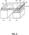
- Fig. 4 is a perspective view showing the mounting structure of the semiconductor current reduction device according to the first embodiment of the present invention.
- the switching device Q7 that is disposed on a cooler 108 is disposed opposite to the current decreasing resistor 104 with a certain spacing.
- the space between the switching device Q7 and the current decreasing resistor 104 is formed as an air duct 110 that keeps the switching device Q7 apart from the current decreasing resistor 104.
- a positive-side bus bar 106 and a negative-side bus bar 107 are disposed opposite and apart from each other.
- the positive-side bus bar 106 and the negative-side bus bar 107 are formed in a nearly planar shape using a copper plate member, and are configured as wires that connect the switching device Q7 to the current decreasing resistor 104.
- the switching device Q7 is electrically connected to the current decreasing resistor 104 using a plurality of wires.
- the plurality of wires is composed of the positive-side bus bar (first bus bar) 106 that is a first wire and that connects the electrode (the collector) of the switching device Q7 on the high-potential side (the high-potential side in the power running of the rail car 8) to one end of the current decreasing resistor 104 and the negative-side bus bar (second bus bar) 107 that is a second wire and that connects the electrode (the emitter) of the switching device Q7 on the low-potential side (the low-potential side in the power running of the rail car 8) to the other end of the current decreasing resistor 104, in which the positive-side bus bar 106 and the negative-side bus bar 107 are disposed opposite to each other, being stacked.
- the positive-side bus bar 106 and the negative-side bus bar 107 are configured in which when the switching device Q7 is transitioned from on to off, electric current
- connection terminal 106a that is connected to the collector (electrode) of the switching device Q7 is fastened and a connection terminal 106b that is connected to one end of the current decreasing resistor 104 (the high-potential side) is fastened.
- connection terminal 107a that is connected to the other end of the current decreasing resistor 104 (the low-potential side) is fastened through the through hole (not shown) of the positive-side bus bar 106 and a connection terminal 107b that is connected to the emitter (electrode) of the switching device Q7 is fastened through the through hole (not shown) of the positive-side bus bar 106.
- both sides (both end sides in the longitudinal direction) of the positive-side bus bar 106 are connected to the electrode (the collector) of the switching device Q7 on the high-potential side through the connection terminal 106a or to one end of the current decreasing resistor 104 through the connection terminal 106b, and both sides (both end sides in the longitudinal direction) of the negative-side bus bar 107 are connected to the electrode (the emitter) of the switching device Q7 on the low-potential side through the connection terminal 107b or to the other end of the current decreasing resistor 104 through the connection terminal 107a.
- connection terminal 106a when the switching device Q7 is transitioned from on to off, an electric current is carried from the connection terminal 106a to the connection terminal 106b through the positive-side bus bar 106, and this electric current is carried from the connection terminal 107a through the current decreasing resistor 104 to the connection terminal 107b through the negative-side bus bar 107.
- the positive-side bus bar 106 and the negative-side bus bar 107 are stacked opposite and apart from each other, the directions of the electric current carried through the positive-side bus bar 106 and the electric current carried through the negative-side bus bar 107 are reverse to each other.
- the magnetic flux due to the electric current carried through the positive-side bus bar 106 and the magnetic flux due to the electric current carried through the negative-side bus bar 107 are cancelled to each other, and the values of the parasitic inductance of the positive-side bus bar 106 and the negative-side bus bar 107 can be reduced. That is, closely disposing the positive-side bus bar 106 and the negative-side bus bar 107, through which the electric currents in the reverse orientations are carried, can reduce a magnetic field to be generated, and the parasitic inductance of the wire can be reduced. Note that the arrows in the drawing express the orientations of electric currents that are carried.
- the parasitic inductances of the positive-side bus bar 106 and the negative-side bus bar 107 can be reduced, and as a result, the surge voltage due to the parasitic inductance of the wire can be reduced.
- the current decreasing resistor 104 can operate at a temperature of 200°C or more, whereas the operating temperature of the switching device Q7 is about 125°C. That is, it is necessary to thermally insulate the current decreasing resistor 104 from the switching device Q7. Therefore, in the first embodiment, the space between the current decreasing resistor 104 and the switching device Q7 is formed in the air duct 110 through which air is carried, and thus the current decreasing resistor 104 can be cooled by air carried through the air duct 110, and the switching device Q7, the positive-side bus bar 106, and the negative-side bus bar 107 can be cooled.
- the distance between the current decreasing resistor 104 and the switching device Q7 is kept apart from each other, and thus the breakage of the switching device Q7 due to induced electromotive force can be prevented while thermal insulation is provided (conducting the heat of the current decreasing resistor 104 to the switching device Q7 is suppressed).
- the thickness of a chip that is installed on the switching device Q7 can be made thin. That is, since a conduction loss can be reduced, the cooler 108 of the switching device Q7 can be reduced in size.
- the surge voltage due to the parasitic inductance of the wire that connects the switching device Q7 to the current decreasing resistor 104 can be reduced as well as the thermal insulation effect can be improved by keeping the distance between the current decreasing resistor 104 and the switching device Q7 apart.
- Fig. 5 is a perspective view showing the mounting structure of a semiconductor current reduction device according to a second embodiment of the present invention.
- the operation of a semiconductor current reduction device 10 according to the second embodiment is similar to the first embodiment, and the description is omitted.
- the parasitic inductance can be more reduced as the current distributions of a positive-side bus bar 106 and a negative-side bus bar 107 that connect a current decreasing resistor 104 to a switching device Q7 are made more equal. more specifically, it is effective to make the current distributions near the connection terminals that connect the current decreasing resistor 104 to the positive-side bus bar 106 and the negative-side bus bar 107 equal.
- connection terminals 106b and 106c and connection terminals 107a and 107c that respectively connect the current decreasing resistor 104 to the positive-side bus bar 106 and the negative-side bus bar 107 are disposed in a staggered configuration. That is, the connection terminals having different connection destinations (the positive-side bus bar 106 or the negative-side bus bar 107) are alternately disposed. At this time, the connection terminals 106b and 106c are fastened to the back surface side of the positive-side bus bar 106, and connected to one end of the current decreasing resistor 104 (the high-potential side).
- connection terminals 107a and 107c are fastened to the back surface side of the negative-side bus bar 107 through the through hole (not shown) of the positive-side bus bar 106, and connected to the other end of the current decreasing resistor 104 (the low-potential side).
- connection terminals 106b and 106c and the connection terminals 107a and 107c in a staggered configuration achieves the effect that can make the current distributions of the positive-side bus bar 106 and the negative-side bus bar 107 near these connection terminals equal and that more reduces the parasitic inductances of the positive-side bus bar 106 and the negative-side bus bar 107.
- a plurality of connection terminals (connection terminals including connection terminals 106a and 107b) that connects the switching device Q7 to the positive-side bus bar 106 and the negative-side bus bar 107 an also be disposed in a staggered configuration.
- the current distributions of the positive-side bus bar 106 and the negative-side bus bar 107 near the connection terminals including the connection terminals 106a and 107b can be mad equal, and the parasitic inductances of the positive-side bus bar 106 and the negative-side bus bar 107 can be more reduced.
- the effect similar to the first embodiment can be exerted, and the current distributions of the positive-side bus bar 106 and the negative-side bus bar 107 near the connection terminals disposed in a staggered configuration can be mad equal, and the parasitic inductances of the positive-side bus bar 106 and the negative-side bus bar 107 can be reduced more than in the first embodiment.
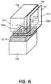
- Fig. 6 is a perspective view showing the mounting structure of a semiconductor current reduction device according to a second embodiment of the present invention.
- a positive-side bus bar 106 and a negative-side bus bar 107 according to the third embodiment are bus bars configured in which a conductive bus bar in a planar shape (a bus bar that is equivalent to the positive-side or the negative-side bus bar according to the first embodiment) is bent at a nearly right angle at almost the center in its longitudinal direction and formed in an L-shape, and the other configurations and the operation of the semiconductor current reduction device 10 are similar to those of the first embodiment, and the description for these points is omitted.
- the positive-side bus bar 106 and the negative-side bus bar 107 that connect a current decreasing resistor 104 to a switching device Q7 are stacked, and electric currents in reverse directions are carried through the positive-side bus bar 106 and the negative-side bus bar 107.
- the parasitic inductances of the positive-side bus bar 106 and the negative-side bus bar 107 can be reduced. Therefore, the positive-side bus bar 106 and the negative-side bus bar 107 may be bent, which are not in a linear shape (in a planar shape) .
- the number of bends may be twice, which is not necessarily once.
- the switching device Q7 Since the positive-side bus bar 106 and the negative-side bus bar 107 are bent, the switching device Q7, the following is enabled in which the current decreasing resistor 104, and the positive-side bus bar 106 and the negative-side bus bar 107 are collectively accommodated in a box or in a frame body, the box or the frame body is disposed on the inner side of the car body that is the main body of a rail car 8, and a cooler 108 is disposed on the outer side of the car body.
- the semiconductor current reduction device 10 can be more easily mounted on the car body than in the first embodiment.
- an air duct 110 can also be formed in the space between the current decreasing resistor 104 and the switching device Q7.
- the effect similar to the first embodiment can be exerted, and mounting the semiconductor current reduction device 10 is made easier than in the first embodiment.
- the present invention is not limited to the above-described embodiments, and includes various exemplary modifications.
- the current sensor 12 and the control circuit 13 can also be disposed on the semiconductor current reduction device 10.
- a control circuit that integrates the current sensor 12 with the control circuit 13 can be configured.
- the turning on and off of the switching device Q7 is controlled based on the electric current carried through the contactor 11 (the switching device Q7 is turned on when the electric current is less than a set value, and turned off when the electric current is the set value or more), this shortens the delay time of interruption by the contactor 11, and lowering the breaking current is made possible.
- a device can be configured as a breaking device, including a line breaker that is disposed between a direct current overhead contact line and a power converter and that interrupts electric power supplied from the direct current overhead contact line to the power converter, a current sensor that detects the electric current carried through the line breaker, a switching device that is disposed between the line breaker and the power converter and that supplies electric power from the line breaker to the power converter when the switching device is in its on-operation, a resister that is connected in parallel to the switching device through a plurality of wires, and a control circuit that controls the switching device to be turned off from on and then controls the line breaker to be interrupted when an electric current detected by the current sensor is a set value or more.
- the plurality of wires includes a first wire that connects a high-potential side electrode of the switching device to one end of the resister and a second wire that connects a low-potential side electrode of the switching device to another end of the resister.
- the first wire and the second wire are disposed opposite to each other being stacked. Through the first wire and the second wire, electric currents in reverse directions are carried when the switching device is transitioned from on to off.
- a part of the configuration of an embodiment can be replaced by the configuration of another embodiment, and the configuration of another embodiment can be added to the configuration of an embodiment.
- another configuration can be added, removed, or replaced.
Landscapes
- Engineering & Computer Science (AREA)
- Power Engineering (AREA)
- Life Sciences & Earth Sciences (AREA)
- Sustainable Development (AREA)
- Sustainable Energy (AREA)
- Transportation (AREA)
- Mechanical Engineering (AREA)
- Electric Propulsion And Braking For Vehicles (AREA)
- Inverter Devices (AREA)
- Power Conversion In General (AREA)
Abstract
Description
- The present invention relates to a current reduction device that is disposed between a line breaker and a power converter.
- On the underfloor of a railway vehicle, a power converter and a filter reactor, which are driving electric devices, and further a signaling device, are installed. Nowadays, in order to improve the maintenability of rail cars, it is considered to install monitoring devices that grasp the degradation and failures of rail car devices or facilities. Since the underfloor space of the railway vehicle has limitations, in order to newly install these monitoring devices on the rail car, it is necessary to reduce the sizes of driving electric devices. In the power converter, an IGBT (Insulated Gate Bipolar Transistor) and a MOSFET (Metal-Oxide-Semiconductor Field-Effect Transistor), which are voltage drive power semiconductors, are applied. The power semiconductors including the IGBT and the MOSFET can reduce switching losses by a high-speed switching operation, and can reduce generated losses, and thus the cooler of the power converter can be reduced in size.
- In order to reduce the size of a filter reactor, a reduction in its inductance value is effective. However, a reduction in the inductance value increases an electric current per unit time, the electric current flowing from an overhead contact line when the power converter is broken or when a ground fault occurs . Generally, this large electric current is interrupted by a mechanical device, such as a high speed circuit breaker. However, since a reduction in the inductance value increases the electric current per unit time, this leads to a concern that the allowable current in an electric power substation might be exceeded at the breaking speed of a mechanical circuit breaker. Therefore, it is considered that the combination of a semiconductor current limiter and a mechanical circuit breaker increases the breaking speed, compared with using a mechanical circuit breaker alone, and this enables the compatibility of a reduction in the inductance value of the filter reactor with a reduction in the breaking current.
- As the background of the present technical field, there is Japanese Unexamined Patent Application Publication No.
2004-96877 - Patent Literature 1: Japanese Patent Application Laid-Open No.
2004-96877 - In
Patent Literature 1, in the case in which the inverter causes an arm short circuit failure, the switching device is turned off, an overcurrent is decreased by the resistor, and the contactor is then opened to interrupt the fault current. Here, when the switching device is turned off, a surge voltage occurs due to the parasitic inductance of a wire that connects the switching device to the resistor. When this surge voltage exceeds the rated voltage of the switching device, the switching device is broken. In order to reduce the parasitic inductance that is a cause of the surge voltage, shortening the wire is effective. On the other hand, although the operating temperature of the resistor is 200°C or more, the operating temperature of the switching device is about 125°C. Thus, it is desirable to keep the distance between the resistor and the switching device apart from each other for thermal insulation. - An object of the present invention is to reduce a surge voltage due to the parasitic inductance of a wire that connects a switching device to a resister.
- In order to solve the object, the present invention is a current reduction device including: a switching device that is disposed between a line breaker configured to interrupt electric power supplied from a direct current overhead contact line to a power converter and the power converter, the switching device being configured to supply electric power from the line breaker to the power converter when the switching device is in on-operation; and a resister that is connected in parallel to the switching device through a plurality of wires. In the device, the plurality of wires includes a first wire configured to connect a high-potential side electrode of the switching device to one end of the resister, and a second wire configured to connect a low-potential side electrode of the switching device to another end of the resister; the first wire and the second wire are disposed opposite to each other being stacked; and through the first wire and the second wire, electric currents in reverse directions are carried when the switching device is transitioned from on to off.
- According to the present invention, a surge voltage due to the parasitic inductance of a wire that connects a switching device to a resister can be reduced.
-
-
Fig. 1 is a schematic diagram of an electric motor car according to a first embodiment of the present invention. -
Fig. 2 is a circuit block diagram showing the overall structure of a driving device according to the first embodiment of the present invention. -
Fig. 3 is a circuit block diagram including the overall structure of the driving device and the equivalent circuit of a semiconductor current reduction device according to the first embodiment of the present invention. -
Fig. 4 is a perspective view showing the mounting structure of the semiconductor current reduction device according to the first embodiment of the present invention. -
Fig. 5 is a perspective view showing the mounting structure of a semiconductor current reduction device according to a second embodiment of the present invention. -
Fig. 6 is a perspective view showing the mounting structure of a semiconductor current reduction device according to a third embodiment of the present invention. - In the following, embodiments will be described with reference to the drawings. Note that in the drawings and the embodiments, a MOSFET is taken as a switching device. However, the present invention is also applicable to an IGBT.
-
Fig. 1 is a schematic diagram of an electric motor car according to a first embodiment of the present invention. InFig. 1 , in a power running operation that accelerates an electric motor car, electric power is supplied to arail car 8 from an overhead contact line (direct current overhead contact line) 1 that is a power source through acurrent collector 7. The electric power supplied to therail car 8 is subjected to direct-current-to-alternating-current power conversion through acontactor 11, a semiconductorcurrent reduction device 10, afilter reactor 9, and apower converter 6, and themotor 5 is driven by the converted alternating-current power.Wheels 3 rotate by the drive of themotor 5, and therail car 8 goes forward. Themotor 5 may be an induction motor or a permanent magnet synchronous motor, any of which is fine. In a regenerative operation that decelerates the electric motor car, the electric power flow is inverted to the electric power flow in the power running operation. That is, themotor 5 operates as a power generator, electric power is subjected to alternating-current-to-direct-current power conversion by thepower converter 6, and then electric power is regenerated to theoverhead contact line 1 through thefilter reactor 9 and thecurrent collector 7. Note that as an electrical ground, the negative voltage side of thepower converter 6 is connected to arail 2 through thewheel 3. Here, for the voltage of theoverhead contact line 1, as an example, an embodiment will be described in which a direct current of 1,500 V is used as a power supply. Themotor 5 is installed on a bogie 4, and the bogie 4 supports therail car 8. -
Fig. 2 is a circuit block diagram showing the overall structure of a driving device according to the first embodiment of the present invention. InFig. 2 , a driving device that drives themotor 5 includes thepower converter 6. Thepower converter 6 includes acapacitor 103 and switching devices Q1 to Q6 as a direct-current-to-alternating-current power converter. The switching devices Q1 and Q2 are connected in series to form a U-phase, the switching devices Q3 and Q4 are connected in series to form a V-phase, and the switching devices Q5 and Q6 are connected in series to form a W-phase. To the switching devices Q1 to Q6, diodes D1 to D6 are connected in parallel such that a conduction direction is a reverse direction. Here, in the case in which the switching devices Q1 to Q6 are IGBTs, it is necessary to connect the diodes D1 to D6. However, in the case in which the switching devices Q1 to Q6 are devices having a body diode, such as a MOSFET, the body diode of the MOSFET can be used without connecting the diodes D1 to D6. A 2-in-1 device may be used in which switching devices or diodes connected in series are installed on the same package. - The
power converter 6 includes thecapacitor 103 that smooths direct current power obtained from theoverhead contact line 1 and that removes noise. The switching devices Q1 to Q6 in the U-phase, the V-phase, and the W-phase respond to PWM (Pulse Width Modulation) control signals from a switching controller (not shown), for example, for switching operations, and thus converts the direct current power of thecapacitor 103 to alternating-current powers and supplies the converted alternating-current power to themotor 5. - The
power converter 6 is connected to the semiconductorcurrent reduction device 10 through thefilter reactor 9. The semiconductorcurrent reduction device 10 is composed of a switching device Q7, an anti-parallel diode D7 of the switching device Q7, and acurrent decreasing resistor 104. In the switching device Q7, the emitter (electrode) is connected to thepower converter 6 through thefilter reactor 9, the collector (electrode) is connected to theoverhead contact line 1 through acurrent sensor 12, thecontactor 11, and thecurrent collector 7, and the gate (electrode) is connected to thecontrol circuit 13. Thiscontrol circuit 13 is connected to thecurrent sensor 12 and thecontactor 11. Thecontrol circuit 13 is configured in which in the case in which thecurrent sensor 12 detects a ground fault electric current, thecontrol circuit 13 controls the switching device Q7 from on to off, and then interrupts thecontactor 11. Note that in the case in which the switching device Q7 is a MOSFET, the anti-parallel diode does not necessarily have to be installed. To the switching device Q7, a cooler (not shown) is connected, and the switching device Q7 is cooled by the cooler. - Here, for example, in the case in which a ground fault occurs in the subsequent stage of the
filter reactor 9 when viewed from theoverhead contact line 1, a ground fault electric current occurs from theoverhead contact line 1 through thefilter reactor 9. The slope of this ground fault electric current that is increased with time is calculated by the division of the voltage of theoverhead contact line 1 by the inductance value of thefilter reactor 9 when the resistance component of the reactor or the other wire is ignored. That is, the slope of the ground fault electric current that is increased becomes steeper as the inductance value of thefilter reactor 9 is smaller. At this time, although an increase in the inductance value of thefilter reactor 9 can suppress a steep slope of the ground fault electric current that is increased, thefilter reactor 9 is increased in size. Therefore, as thefilter reactor 9, one having a small inductance value is used. - Next, the operation of interrupting this ground fault electric current using the semiconductor
current reduction device 10 will be described. The on/off state of the switching device Q7 is controlled by thecontrol circuit 13 based on the detection value of the current sensor 12 (the current value of the contactor 11) . For example, in the case in which the set value that turns off the switching device Q7 is set to 2,000 A or more, when the detection value of thecurrent sensor 12 is less than 2,000 A, thecontrol circuit 13 maintains the switching device Q7 in an ON-state, whereas when the ground fault electric current that is the detection value of thecurrent sensor 12 is 2, 000 A or more, thecontrol circuit 13 performs control that transitions the state of the switching device Q7 from on to off. - When the switching device Q7 is turned to the OFF-state, the ground fault electric current is carried through the current decreasing
resistor 104 that is connected in parallel to the switching device Q7. This ground fault electric current is decreased by the current decreasingresistor 10. For example, it is assumed that the voltage of theoverhead contact line 1 is 1,500 V and the resistance value of the current decreasingresistor 104 is three ohms, the electric current after decreased is 500 A. As a result, since the ground fault electric current is decreased from 2,000 A, at which the electric current is an electric current immediately after the ground fault occurs, to 500 A, thecontrol circuit 13 performs control that interrupts thecontactor 11, and protects an electric power substation. At this time, the contactor 11 functions as a line breaker or a circuit breaker that interrupts electric power supplied from theoverhead contact line 1 to thepower converter 6. - The switching devices Q1 to Q7 may be a voltage control switching device, such as a MOSFET and an IGBT, or an electric current control switching device, such as a thyristor. The diodes D1 to D7 may be a PN diode, an SBD (Schottky Barrier Diode), and the like. The switching devices Q1 to Q7 may include a plurality of types of switching devices, such as a MOSFET and an IGBT, and the base material of the semiconductor material may be SiC (Silicon Carbide) or GaN (Gallium Nitride), which are semiconductors having a band gap wider than the band gap of Si (Silicon).
-
Fig. 3 is a circuit block diagram including the overall structure of the driving device and the equivalent circuit of the semiconductor current reduction device according to the first embodiment of the present invention. InFig. 3 , in connecting the current decreasingresistor 104 that is a resister in parallel to the switching device Q7 of the semiconductorcurrent reduction device 10, it is necessary to electrically connect the switching device Q7 to the current decreasingresistor 104 using a plurality of wires. Here, on the wires, parasitic inductances 105a and 105b are present, and induced electromotive force occurs on the parasitic inductances 105a and 105b in association with a change in the electric current. - Next, the influence of the parasitic inductances 105a and 105b in the semiconductor
current reduction device 10 is considered. When a ground fault occurs on a circuit that connects thepower converter 6 to therail 2 and the switching device Q7 is transitioned from the ON-state to the OFF-state, the large electric current is commutated from the switching device Q7 to the current decreasingresistor 104. In association with a change in this electric current, induced electromotive force occurs in the parasitic inductances 105a and 105b. On the current decreasingresistor 104, a voltage that is a product of the electric current and the resistance value occurs. The sum of these induced electromotive forces and the voltage on the current decreasingresistor 104 is applied across the collector and the emitter of the switching device Q7. Since the induced electromotive force is more increased as the electric current that is commutated is larger, in order to prevent the switching device Q7 from being broken, it is necessary to reduce the parasitic inductances 105a and 105b. -
Fig. 4 is a perspective view showing the mounting structure of the semiconductor current reduction device according to the first embodiment of the present invention. InFig. 4 , the switching device Q7 that is disposed on a cooler 108 is disposed opposite to the current decreasingresistor 104 with a certain spacing. At this time, the space between the switching device Q7 and the current decreasingresistor 104 is formed as anair duct 110 that keeps the switching device Q7 apart from the current decreasingresistor 104. Above the switching device Q7 and the current decreasingresistor 104, a positive-side bus bar 106 and a negative-side bus bar 107 are disposed opposite and apart from each other. The positive-side bus bar 106 and the negative-side bus bar 107 are formed in a nearly planar shape using a copper plate member, and are configured as wires that connect the switching device Q7 to the current decreasingresistor 104. - That is, the switching device Q7 is electrically connected to the current decreasing
resistor 104 using a plurality of wires. At this time, the plurality of wires is composed of the positive-side bus bar (first bus bar) 106 that is a first wire and that connects the electrode (the collector) of the switching device Q7 on the high-potential side (the high-potential side in the power running of the rail car 8) to one end of the current decreasingresistor 104 and the negative-side bus bar (second bus bar) 107 that is a second wire and that connects the electrode (the emitter) of the switching device Q7 on the low-potential side (the low-potential side in the power running of the rail car 8) to the other end of the current decreasingresistor 104, in which the positive-side bus bar 106 and the negative-side bus bar 107 are disposed opposite to each other, being stacked. The positive-side bus bar 106 and the negative-side bus bar 107 are configured in which when the switching device Q7 is transitioned from on to off, electric currents in reverse directions are carried though the positive-side bus bar 106 and the negative-side bus bar 107. - More specifically, to the back surface side of the positive-
side bus bar 106, aconnection terminal 106a that is connected to the collector (electrode) of the switching device Q7 is fastened and aconnection terminal 106b that is connected to one end of the current decreasing resistor 104 (the high-potential side) is fastened. On the other hand, to the back surface side of the negative-side bus bar 107, aconnection terminal 107a that is connected to the other end of the current decreasing resistor 104 (the low-potential side) is fastened through the through hole (not shown) of the positive-side bus bar 106 and aconnection terminal 107b that is connected to the emitter (electrode) of the switching device Q7 is fastened through the through hole (not shown) of the positive-side bus bar 106. At this time, both sides (both end sides in the longitudinal direction) of the positive-side bus bar 106 are connected to the electrode (the collector) of the switching device Q7 on the high-potential side through theconnection terminal 106a or to one end of the current decreasingresistor 104 through theconnection terminal 106b, and both sides (both end sides in the longitudinal direction) of the negative-side bus bar 107 are connected to the electrode (the emitter) of the switching device Q7 on the low-potential side through theconnection terminal 107b or to the other end of the current decreasingresistor 104 through theconnection terminal 107a. - Here, when the switching device Q7 is transitioned from on to off, an electric current is carried from the
connection terminal 106a to theconnection terminal 106b through the positive-side bus bar 106, and this electric current is carried from theconnection terminal 107a through the current decreasingresistor 104 to theconnection terminal 107b through the negative-side bus bar 107. In this case, since the positive-side bus bar 106 and the negative-side bus bar 107 are stacked opposite and apart from each other, the directions of the electric current carried through the positive-side bus bar 106 and the electric current carried through the negative-side bus bar 107 are reverse to each other. Therefore, the magnetic flux due to the electric current carried through the positive-side bus bar 106 and the magnetic flux due to the electric current carried through the negative-side bus bar 107 are cancelled to each other, and the values of the parasitic inductance of the positive-side bus bar 106 and the negative-side bus bar 107 can be reduced. That is, closely disposing the positive-side bus bar 106 and the negative-side bus bar 107, through which the electric currents in the reverse orientations are carried, can reduce a magnetic field to be generated, and the parasitic inductance of the wire can be reduced. Note that the arrows in the drawing express the orientations of electric currents that are carried. - In the present structure, since the electric currents in the reverse orientations are carried even though the wire length of the positive-
side bus bar 106 and the negative-side bus bar 107 are increased, the parasitic inductances of the positive-side bus bar 106 and the negative-side bus bar 107 can be reduced, and as a result, the surge voltage due to the parasitic inductance of the wire can be reduced. - On the other hand, when a large electric current of about 2,000 A is carried through the current decreasing
resistor 104, heat generation occurs. The current decreasingresistor 104 can operate at a temperature of 200°C or more, whereas the operating temperature of the switching device Q7 is about 125°C. That is, it is necessary to thermally insulate the current decreasingresistor 104 from the switching device Q7. Therefore, in the first embodiment, the space between the current decreasingresistor 104 and the switching device Q7 is formed in theair duct 110 through which air is carried, and thus the current decreasingresistor 104 can be cooled by air carried through theair duct 110, and the switching device Q7, the positive-side bus bar 106, and the negative-side bus bar 107 can be cooled. That is, the distance between the current decreasingresistor 104 and the switching device Q7 is kept apart from each other, and thus the breakage of the switching device Q7 due to induced electromotive force can be prevented while thermal insulation is provided (conducting the heat of the current decreasingresistor 104 to the switching device Q7 is suppressed). - In the case in which a semiconductor material having a band gap wider than the band gap of Si is used for the switching device Q7 (e.g. SiC), the thickness of a chip that is installed on the switching device Q7 can be made thin. That is, since a conduction loss can be reduced, the cooler 108 of the switching device Q7 can be reduced in size.
- In the case in which a MOSFET is used for the switching device Q7, no built-in voltage occurs unlike the IGBT, and thus the conduction loss in a low-electric current can be reduced, compared with the IGBT. As a result, the cooler 108 that cools the switching device Q7 can be reduced in size.
- According to the present embodiment, the surge voltage due to the parasitic inductance of the wire that connects the switching device Q7 to the current decreasing
resistor 104 can be reduced as well as the thermal insulation effect can be improved by keeping the distance between the current decreasingresistor 104 and the switching device Q7 apart. -
Fig. 5 is a perspective view showing the mounting structure of a semiconductor current reduction device according to a second embodiment of the present invention. InFig. 5 , the operation of a semiconductorcurrent reduction device 10 according to the second embodiment is similar to the first embodiment, and the description is omitted. - The parasitic inductance can be more reduced as the current distributions of a positive-
side bus bar 106 and a negative-side bus bar 107 that connect a current decreasingresistor 104 to a switching device Q7 are made more equal. more specifically, it is effective to make the current distributions near the connection terminals that connect the current decreasingresistor 104 to the positive-side bus bar 106 and the negative-side bus bar 107 equal. - In the present embodiment,
connection terminals connection terminals resistor 104 to the positive-side bus bar 106 and the negative-side bus bar 107 are disposed in a staggered configuration. That is, the connection terminals having different connection destinations (the positive-side bus bar 106 or the negative-side bus bar 107) are alternately disposed. At this time, theconnection terminals side bus bar 106, and connected to one end of the current decreasing resistor 104 (the high-potential side). Theconnection terminals side bus bar 107 through the through hole (not shown) of the positive-side bus bar 106, and connected to the other end of the current decreasing resistor 104 (the low-potential side). - Disposing the
connection terminals connection terminals side bus bar 106 and the negative-side bus bar 107 near these connection terminals equal and that more reduces the parasitic inductances of the positive-side bus bar 106 and the negative-side bus bar 107. Note that a plurality of connection terminals (connection terminals includingconnection terminals side bus bar 106 and the negative-side bus bar 107 an also be disposed in a staggered configuration. In this case, the current distributions of the positive-side bus bar 106 and the negative-side bus bar 107 near the connection terminals including theconnection terminals side bus bar 106 and the negative-side bus bar 107 can be more reduced. - According to the present embodiment, the effect similar to the first embodiment can be exerted, and the current distributions of the positive-
side bus bar 106 and the negative-side bus bar 107 near the connection terminals disposed in a staggered configuration can be mad equal, and the parasitic inductances of the positive-side bus bar 106 and the negative-side bus bar 107 can be reduced more than in the first embodiment. -
Fig. 6 is a perspective view showing the mounting structure of a semiconductor current reduction device according to a second embodiment of the present invention. InFig. 6 , a positive-side bus bar 106 and a negative-side bus bar 107 according to the third embodiment are bus bars configured in which a conductive bus bar in a planar shape (a bus bar that is equivalent to the positive-side or the negative-side bus bar according to the first embodiment) is bent at a nearly right angle at almost the center in its longitudinal direction and formed in an L-shape, and the other configurations and the operation of the semiconductorcurrent reduction device 10 are similar to those of the first embodiment, and the description for these points is omitted. - The positive-
side bus bar 106 and the negative-side bus bar 107 that connect a current decreasingresistor 104 to a switching device Q7 are stacked, and electric currents in reverse directions are carried through the positive-side bus bar 106 and the negative-side bus bar 107. Thus, the parasitic inductances of the positive-side bus bar 106 and the negative-side bus bar 107 can be reduced. Therefore, the positive-side bus bar 106 and the negative-side bus bar 107 may be bent, which are not in a linear shape (in a planar shape) . The number of bends may be twice, which is not necessarily once. Since the positive-side bus bar 106 and the negative-side bus bar 107 are bent, the switching device Q7, the following is enabled in which the current decreasingresistor 104, and the positive-side bus bar 106 and the negative-side bus bar 107 are collectively accommodated in a box or in a frame body, the box or the frame body is disposed on the inner side of the car body that is the main body of arail car 8, and a cooler 108 is disposed on the outer side of the car body. Thus, the semiconductorcurrent reduction device 10 can be more easily mounted on the car body than in the first embodiment. Note that also in the present embodiment, anair duct 110 can also be formed in the space between the current decreasingresistor 104 and the switching device Q7. - According to the present embodiment, the effect similar to the first embodiment can be exerted, and mounting the semiconductor
current reduction device 10 is made easier than in the first embodiment. - Note that the present invention is not limited to the above-described embodiments, and includes various exemplary modifications. For example, the
current sensor 12 and thecontrol circuit 13 can also be disposed on the semiconductorcurrent reduction device 10. A control circuit that integrates thecurrent sensor 12 with thecontrol circuit 13 can be configured. In this case, in the control circuit, for example, the turning on and off of the switching device Q7 is controlled based on the electric current carried through the contactor 11 (the switching device Q7 is turned on when the electric current is less than a set value, and turned off when the electric current is the set value or more), this shortens the delay time of interruption by thecontactor 11, and lowering the breaking current is made possible. A device can be configured as a breaking device, including a line breaker that is disposed between a direct current overhead contact line and a power converter and that interrupts electric power supplied from the direct current overhead contact line to the power converter, a current sensor that detects the electric current carried through the line breaker, a switching device that is disposed between the line breaker and the power converter and that supplies electric power from the line breaker to the power converter when the switching device is in its on-operation, a resister that is connected in parallel to the switching device through a plurality of wires, and a control circuit that controls the switching device to be turned off from on and then controls the line breaker to be interrupted when an electric current detected by the current sensor is a set value or more. In the device, the plurality of wires includes a first wire that connects a high-potential side electrode of the switching device to one end of the resister and a second wire that connects a low-potential side electrode of the switching device to another end of the resister. The first wire and the second wire are disposed opposite to each other being stacked. Through the first wire and the second wire, electric currents in reverse directions are carried when the switching device is transitioned from on to off. - A part of the configuration of an embodiment can be replaced by the configuration of another embodiment, and the configuration of another embodiment can be added to the configuration of an embodiment. In regard to a part of the configuration of each of the embodiments, another configuration can be added, removed, or replaced.
-
- 1:
- overhead contact line
- 2:
- rail
- 3:
- wheel
- 4:
- bogie
- 5:
- motor
- 6:
- power converter
- 7:
- current collector
- 8:
- rail car
- 9:
- filter reactor
- 10:
- semiconductor current reduction device
- 11:
- contactor
- 12:
- current sensor
- 13:
- control circuit
- Q1 to Q7:
- switching device
- D1 to D7:
- diode
- 103:
- capacitor
- 104:
- current decreasing resistor
- 105a, 105b:
- parasitic inductance
- 106:
- positive-side bus bar
- 107:
- negative-side bus bar
- 108:
- cooler
- 110:
- air duct
Claims (8)
- A current reduction device comprising:a switching device that is disposed between a line breaker configured to interrupt electric power supplied from a direct current overhead contact line to a power converter and the power converter, the switching device being configured to supply electric power from the line breaker to the power converter when the switching device is in on-operation; anda resister that is connected in parallel to the switching device through a plurality of wires,wherein: the plurality of wires includesa first wire configured to connect a high-potential side electrode of the switching device to one end of the resister, anda second wire configured to connect a low-potential side electrode of the switching device to another end of the resister;the first wire and the second wire are disposed opposite to each other being stacked; andthrough the first wire and the second wire, electric currents in reverse directions are carried when the switching device is transitioned from on to off.
- The current reduction device according to claim 1,
wherein: the switching device and the resister are disposed apart from each other; and
between the switching device and the resister, an air duct through which air is carried is formed. - The current reduction device according to claim 1 or 2,
wherein: the first wire has a first bus bar, and both sides of the first bus bar are connected to a high-potential side electrode of the switching device or one end of the resister through one or two or more connection terminals;
the second wire has a second bus bar, and both sides of the second bus bar are connected to a low-potential side electrode of the switching device or the other end of the resister through one or two or more connection terminals; and
at least one of the two or more connection terminals that are connected to the high-potential side electrode of the switching device or one end of the resister or the two or more connection terminals that are connected to the low-potential side electrode of the switching device or the other end of the resister are disposed in a staggered configuration. - The current reduction device according to claim 1 or 2,
wherein: the first wire has a first bus bar that is formed by bending at least a part of a bus bar in a planar shape, and both sides of the first bus bar are connected to the high-potential side electrode of the switching device or one end of the resister through one or two or more connection terminals; and
the second wire has a second bus bar that is formed by bending at least a part of the bus bar in a planar shape, and both sides of the second bus bar are connected to the low-potential side electrode of the switching device or the other end of the resister through one or two or more connection terminals. - The current reduction device according to claim 4,
wherein at least one of the two or more connection terminals that are connected to the high-potential side electrode of the switching device or one end of the resister or the two or more connection terminals that are connected to the low-potential side electrode of the switching device or the other end of the resister are disposed in a staggered configuration. - The current reduction device according to any one of claims 1 to 5,
wherein the switching device is configured using silicon or a semiconductor material having a band gap greater than a band gap of silicon as a base material. - The current reduction device according to any one of claims 1 to 6,
wherein the switching device is a voltage drive device that is a MOSFET or an IGBT. - The current reduction device according to any one of claims 1 to 7, further comprising
a control circuit configured to control turning on and off of the switching device based on an electric current on the line breaker.
Applications Claiming Priority (2)
| Application Number | Priority Date | Filing Date | Title |
|---|---|---|---|
| JP2017224662A JP6906431B2 (en) | 2017-11-22 | 2017-11-22 | Flow reducer |
| PCT/JP2018/041883 WO2019102896A1 (en) | 2017-11-22 | 2018-11-12 | Current reduction device |
Publications (3)
| Publication Number | Publication Date |
|---|---|
| EP3716463A1 true EP3716463A1 (en) | 2020-09-30 |
| EP3716463A4 EP3716463A4 (en) | 2021-09-08 |
| EP3716463B1 EP3716463B1 (en) | 2023-09-20 |
Family
ID=66630934
Family Applications (1)
| Application Number | Title | Priority Date | Filing Date |
|---|---|---|---|
| EP18881549.2A Active EP3716463B1 (en) | 2017-11-22 | 2018-11-12 | Current reduction device |
Country Status (3)
| Country | Link |
|---|---|
| EP (1) | EP3716463B1 (en) |
| JP (1) | JP6906431B2 (en) |
| WO (1) | WO2019102896A1 (en) |
Families Citing this family (2)
| Publication number | Priority date | Publication date | Assignee | Title |
|---|---|---|---|---|
| JP7289774B2 (en) * | 2019-10-31 | 2023-06-12 | 株式会社日立製作所 | RAIL VEHICLE DRIVING SYSTEM AND RAIL VEHICLE DRIVING METHOD |
| FR3119927B1 (en) * | 2021-02-17 | 2023-07-28 | Alstom Transp Tech | Electrical connector, electrical system comprising such a connector and railway vehicle comprising such a system |
Family Cites Families (6)
| Publication number | Priority date | Publication date | Assignee | Title |
|---|---|---|---|---|
| JP2001037004A (en) * | 1999-07-26 | 2001-02-09 | Hitachi Ltd | Inverter type electric car control device |
| JP3895239B2 (en) | 2002-08-30 | 2007-03-22 | 株式会社東芝 | Electric vehicle power supply |
| JP2005237118A (en) * | 2004-02-19 | 2005-09-02 | Toyota Motor Corp | Bus bar structure and power converter using the same |
| JP2006067732A (en) * | 2004-08-27 | 2006-03-09 | Toshiba Corp | Electric vehicle control device |
| JP5114350B2 (en) * | 2008-09-12 | 2013-01-09 | 株式会社日立産機システム | Inverter device |
| JP6457800B2 (en) * | 2014-11-28 | 2019-01-23 | 株式会社日立製作所 | Power conversion device and railway vehicle equipped with the same |
-
2017
- 2017-11-22 JP JP2017224662A patent/JP6906431B2/en active Active
-
2018
- 2018-11-12 EP EP18881549.2A patent/EP3716463B1/en active Active
- 2018-11-12 WO PCT/JP2018/041883 patent/WO2019102896A1/en not_active Ceased
Also Published As
| Publication number | Publication date |
|---|---|
| EP3716463B1 (en) | 2023-09-20 |
| JP2019097298A (en) | 2019-06-20 |
| EP3716463A4 (en) | 2021-09-08 |
| JP6906431B2 (en) | 2021-07-21 |
| WO2019102896A1 (en) | 2019-05-31 |
Similar Documents
| Publication | Publication Date | Title |
|---|---|---|
| CN110235244B (en) | Power semiconductor module and power conversion device | |
| EP2966766B1 (en) | Power converter for vehicle | |
| CN103125022B (en) | Power semiconductor modular, power inverter and rolling stock | |
| US9520802B2 (en) | Power semiconductor module, power converting apparatus and railway car | |
| US10134718B2 (en) | Power semiconductor module | |
| JP5851267B2 (en) | Inverter and vehicle control device | |
| US10511301B2 (en) | Gate drive circuit, power conversion apparatus, and railway vehicle | |
| US8644044B2 (en) | Power electronics and integration system for providing a common high current inverter for use with a traction inverter and an auxiliary inverter | |
| CN107148738A (en) | power conversion device | |
| US10554123B2 (en) | Power converter with a parallel flat plate conductor electrically connected with a capacitor and a power module | |
| US11128235B2 (en) | Power conversion device | |
| JP2016103897A (en) | Power conversion device and railway vehicle having the same | |
| AU2018405279B2 (en) | Power conversion device and electric railroad vehicle equipped with power conversion device | |
| WO2019030966A1 (en) | Power conversion device and power conversion method | |
| EP3716463B1 (en) | Current reduction device | |
| JP2013131774A (en) | Power semiconductor module, power conversion device, and rolling stock | |
| US20250150002A1 (en) | Power conversion device | |
| JP4842018B2 (en) | Power converter | |
| JP2017169344A (en) | Power conversion device | |
| WO2019187439A1 (en) | Current reduction device and current reduction method | |
| JP2022014451A (en) | Power supply circuit of vehicle, associated drive line and vehicle | |
| US10937737B2 (en) | Wiring member and power conversion device | |
| US20210159218A1 (en) | Semiconductor module, power conversion device, and movable body | |
| JP2020096431A (en) | Overcurrent detection device |
Legal Events
| Date | Code | Title | Description |
|---|---|---|---|
| STAA | Information on the status of an ep patent application or granted ep patent |
Free format text: STATUS: THE INTERNATIONAL PUBLICATION HAS BEEN MADE |
|
| PUAI | Public reference made under article 153(3) epc to a published international application that has entered the european phase |
Free format text: ORIGINAL CODE: 0009012 |
|
| STAA | Information on the status of an ep patent application or granted ep patent |
Free format text: STATUS: REQUEST FOR EXAMINATION WAS MADE |
|
| 17P | Request for examination filed |
Effective date: 20200622 |
|
| AK | Designated contracting states |
Kind code of ref document: A1 Designated state(s): AL AT BE BG CH CY CZ DE DK EE ES FI FR GB GR HR HU IE IS IT LI LT LU LV MC MK MT NL NO PL PT RO RS SE SI SK SM TR |
|
| AX | Request for extension of the european patent |
Extension state: BA ME |
|
| DAV | Request for validation of the european patent (deleted) | ||
| DAX | Request for extension of the european patent (deleted) | ||
| A4 | Supplementary search report drawn up and despatched |
Effective date: 20210809 |
|
| RIC1 | Information provided on ipc code assigned before grant |
Ipc: B60L 9/18 20060101ALI20210803BHEP Ipc: B60L 3/00 20190101ALI20210803BHEP Ipc: H02M 7/48 20070101AFI20210803BHEP |
|
| REG | Reference to a national code |
Free format text: PREVIOUS MAIN CLASS: H02M0007480000 Ipc: B60L0003040000 Ref country code: DE Ref legal event code: R079 Ref document number: 602018058070 Country of ref document: DE Free format text: PREVIOUS MAIN CLASS: H02M0007480000 Ipc: B60L0003040000 |
|
| RIC1 | Information provided on ipc code assigned before grant |
Ipc: B60L 9/18 20060101ALI20230127BHEP Ipc: H02M 7/00 20060101ALI20230127BHEP Ipc: H02M 1/36 20070101ALI20230127BHEP Ipc: B60L 3/04 20060101AFI20230127BHEP |
|
| GRAP | Despatch of communication of intention to grant a patent |
Free format text: ORIGINAL CODE: EPIDOSNIGR1 |
|
| STAA | Information on the status of an ep patent application or granted ep patent |
Free format text: STATUS: GRANT OF PATENT IS INTENDED |
|
| INTG | Intention to grant announced |
Effective date: 20230403 |
|
| GRAS | Grant fee paid |
Free format text: ORIGINAL CODE: EPIDOSNIGR3 |
|
| GRAA | (expected) grant |
Free format text: ORIGINAL CODE: 0009210 |
|
| STAA | Information on the status of an ep patent application or granted ep patent |
Free format text: STATUS: THE PATENT HAS BEEN GRANTED |
|
| AK | Designated contracting states |
Kind code of ref document: B1 Designated state(s): AL AT BE BG CH CY CZ DE DK EE ES FI FR GB GR HR HU IE IS IT LI LT LU LV MC MK MT NL NO PL PT RO RS SE SI SK SM TR |
|
| REG | Reference to a national code |
Ref country code: GB Ref legal event code: FG4D |
|
| REG | Reference to a national code |
Ref country code: CH Ref legal event code: EP |
|
| REG | Reference to a national code |
Ref country code: DE Ref legal event code: R096 Ref document number: 602018058070 Country of ref document: DE |
|
| REG | Reference to a national code |
Ref country code: IE Ref legal event code: FG4D |
|
| REG | Reference to a national code |
Ref country code: LT Ref legal event code: MG9D |
|
| PG25 | Lapsed in a contracting state [announced via postgrant information from national office to epo] |
Ref country code: GR Free format text: LAPSE BECAUSE OF FAILURE TO SUBMIT A TRANSLATION OF THE DESCRIPTION OR TO PAY THE FEE WITHIN THE PRESCRIBED TIME-LIMIT Effective date: 20231221 |
|
| REG | Reference to a national code |
Ref country code: NL Ref legal event code: MP Effective date: 20230920 |
|
| PG25 | Lapsed in a contracting state [announced via postgrant information from national office to epo] |
Ref country code: SE Free format text: LAPSE BECAUSE OF FAILURE TO SUBMIT A TRANSLATION OF THE DESCRIPTION OR TO PAY THE FEE WITHIN THE PRESCRIBED TIME-LIMIT Effective date: 20230920 Ref country code: RS Free format text: LAPSE BECAUSE OF FAILURE TO SUBMIT A TRANSLATION OF THE DESCRIPTION OR TO PAY THE FEE WITHIN THE PRESCRIBED TIME-LIMIT Effective date: 20230920 Ref country code: NO Free format text: LAPSE BECAUSE OF FAILURE TO SUBMIT A TRANSLATION OF THE DESCRIPTION OR TO PAY THE FEE WITHIN THE PRESCRIBED TIME-LIMIT Effective date: 20231220 Ref country code: LV Free format text: LAPSE BECAUSE OF FAILURE TO SUBMIT A TRANSLATION OF THE DESCRIPTION OR TO PAY THE FEE WITHIN THE PRESCRIBED TIME-LIMIT Effective date: 20230920 Ref country code: LT Free format text: LAPSE BECAUSE OF FAILURE TO SUBMIT A TRANSLATION OF THE DESCRIPTION OR TO PAY THE FEE WITHIN THE PRESCRIBED TIME-LIMIT Effective date: 20230920 Ref country code: HR Free format text: LAPSE BECAUSE OF FAILURE TO SUBMIT A TRANSLATION OF THE DESCRIPTION OR TO PAY THE FEE WITHIN THE PRESCRIBED TIME-LIMIT Effective date: 20230920 Ref country code: GR Free format text: LAPSE BECAUSE OF FAILURE TO SUBMIT A TRANSLATION OF THE DESCRIPTION OR TO PAY THE FEE WITHIN THE PRESCRIBED TIME-LIMIT Effective date: 20231221 Ref country code: FI Free format text: LAPSE BECAUSE OF FAILURE TO SUBMIT A TRANSLATION OF THE DESCRIPTION OR TO PAY THE FEE WITHIN THE PRESCRIBED TIME-LIMIT Effective date: 20230920 |
|
| REG | Reference to a national code |
Ref country code: AT Ref legal event code: MK05 Ref document number: 1613186 Country of ref document: AT Kind code of ref document: T Effective date: 20230920 |
|
| PG25 | Lapsed in a contracting state [announced via postgrant information from national office to epo] |
Ref country code: NL Free format text: LAPSE BECAUSE OF FAILURE TO SUBMIT A TRANSLATION OF THE DESCRIPTION OR TO PAY THE FEE WITHIN THE PRESCRIBED TIME-LIMIT Effective date: 20230920 |
|
| PG25 | Lapsed in a contracting state [announced via postgrant information from national office to epo] |
Ref country code: IS Free format text: LAPSE BECAUSE OF FAILURE TO SUBMIT A TRANSLATION OF THE DESCRIPTION OR TO PAY THE FEE WITHIN THE PRESCRIBED TIME-LIMIT Effective date: 20240120 |
|
| PG25 | Lapsed in a contracting state [announced via postgrant information from national office to epo] |
Ref country code: AT Free format text: LAPSE BECAUSE OF FAILURE TO SUBMIT A TRANSLATION OF THE DESCRIPTION OR TO PAY THE FEE WITHIN THE PRESCRIBED TIME-LIMIT Effective date: 20230920 |
|
| PG25 | Lapsed in a contracting state [announced via postgrant information from national office to epo] |
Ref country code: ES Free format text: LAPSE BECAUSE OF FAILURE TO SUBMIT A TRANSLATION OF THE DESCRIPTION OR TO PAY THE FEE WITHIN THE PRESCRIBED TIME-LIMIT Effective date: 20230920 |
|
| PG25 | Lapsed in a contracting state [announced via postgrant information from national office to epo] |
Ref country code: SM Free format text: LAPSE BECAUSE OF FAILURE TO SUBMIT A TRANSLATION OF THE DESCRIPTION OR TO PAY THE FEE WITHIN THE PRESCRIBED TIME-LIMIT Effective date: 20230920 Ref country code: RO Free format text: LAPSE BECAUSE OF FAILURE TO SUBMIT A TRANSLATION OF THE DESCRIPTION OR TO PAY THE FEE WITHIN THE PRESCRIBED TIME-LIMIT Effective date: 20230920 Ref country code: IS Free format text: LAPSE BECAUSE OF FAILURE TO SUBMIT A TRANSLATION OF THE DESCRIPTION OR TO PAY THE FEE WITHIN THE PRESCRIBED TIME-LIMIT Effective date: 20240120 Ref country code: ES Free format text: LAPSE BECAUSE OF FAILURE TO SUBMIT A TRANSLATION OF THE DESCRIPTION OR TO PAY THE FEE WITHIN THE PRESCRIBED TIME-LIMIT Effective date: 20230920 Ref country code: EE Free format text: LAPSE BECAUSE OF FAILURE TO SUBMIT A TRANSLATION OF THE DESCRIPTION OR TO PAY THE FEE WITHIN THE PRESCRIBED TIME-LIMIT Effective date: 20230920 Ref country code: CZ Free format text: LAPSE BECAUSE OF FAILURE TO SUBMIT A TRANSLATION OF THE DESCRIPTION OR TO PAY THE FEE WITHIN THE PRESCRIBED TIME-LIMIT Effective date: 20230920 Ref country code: AT Free format text: LAPSE BECAUSE OF FAILURE TO SUBMIT A TRANSLATION OF THE DESCRIPTION OR TO PAY THE FEE WITHIN THE PRESCRIBED TIME-LIMIT Effective date: 20230920 Ref country code: PT Free format text: LAPSE BECAUSE OF FAILURE TO SUBMIT A TRANSLATION OF THE DESCRIPTION OR TO PAY THE FEE WITHIN THE PRESCRIBED TIME-LIMIT Effective date: 20240122 Ref country code: SK Free format text: LAPSE BECAUSE OF FAILURE TO SUBMIT A TRANSLATION OF THE DESCRIPTION OR TO PAY THE FEE WITHIN THE PRESCRIBED TIME-LIMIT Effective date: 20230920 |
|
| PG25 | Lapsed in a contracting state [announced via postgrant information from national office to epo] |
Ref country code: PL Free format text: LAPSE BECAUSE OF FAILURE TO SUBMIT A TRANSLATION OF THE DESCRIPTION OR TO PAY THE FEE WITHIN THE PRESCRIBED TIME-LIMIT Effective date: 20230920 |
|
| REG | Reference to a national code |
Ref country code: DE Ref legal event code: R097 Ref document number: 602018058070 Country of ref document: DE |
|
| REG | Reference to a national code |
Ref country code: CH Ref legal event code: PL |
|
| PG25 | Lapsed in a contracting state [announced via postgrant information from national office to epo] |
Ref country code: MC Free format text: LAPSE BECAUSE OF FAILURE TO SUBMIT A TRANSLATION OF THE DESCRIPTION OR TO PAY THE FEE WITHIN THE PRESCRIBED TIME-LIMIT Effective date: 20230920 |
|
| PG25 | Lapsed in a contracting state [announced via postgrant information from national office to epo] |
Ref country code: DK Free format text: LAPSE BECAUSE OF FAILURE TO SUBMIT A TRANSLATION OF THE DESCRIPTION OR TO PAY THE FEE WITHIN THE PRESCRIBED TIME-LIMIT Effective date: 20230920 |
|
| PG25 | Lapsed in a contracting state [announced via postgrant information from national office to epo] |
Ref country code: LU Free format text: LAPSE BECAUSE OF NON-PAYMENT OF DUE FEES Effective date: 20231112 |
|
| PG25 | Lapsed in a contracting state [announced via postgrant information from national office to epo] |
Ref country code: CH Free format text: LAPSE BECAUSE OF NON-PAYMENT OF DUE FEES Effective date: 20231130 |
|
| PLBE | No opposition filed within time limit |
Free format text: ORIGINAL CODE: 0009261 |
|
| STAA | Information on the status of an ep patent application or granted ep patent |
Free format text: STATUS: NO OPPOSITION FILED WITHIN TIME LIMIT |
|
| PG25 | Lapsed in a contracting state [announced via postgrant information from national office to epo] |
Ref country code: MC Free format text: LAPSE BECAUSE OF FAILURE TO SUBMIT A TRANSLATION OF THE DESCRIPTION OR TO PAY THE FEE WITHIN THE PRESCRIBED TIME-LIMIT Effective date: 20230920 Ref country code: LU Free format text: LAPSE BECAUSE OF NON-PAYMENT OF DUE FEES Effective date: 20231112 Ref country code: DK Free format text: LAPSE BECAUSE OF FAILURE TO SUBMIT A TRANSLATION OF THE DESCRIPTION OR TO PAY THE FEE WITHIN THE PRESCRIBED TIME-LIMIT Effective date: 20230920 Ref country code: CH Free format text: LAPSE BECAUSE OF NON-PAYMENT OF DUE FEES Effective date: 20231130 |
|
| REG | Reference to a national code |
Ref country code: BE Ref legal event code: MM Effective date: 20231130 |
|
| 26N | No opposition filed |
Effective date: 20240621 |
|
| REG | Reference to a national code |
Ref country code: IE Ref legal event code: MM4A |
|
| PG25 | Lapsed in a contracting state [announced via postgrant information from national office to epo] |
Ref country code: IE Free format text: LAPSE BECAUSE OF NON-PAYMENT OF DUE FEES Effective date: 20231112 |
|
| PG25 | Lapsed in a contracting state [announced via postgrant information from national office to epo] |
Ref country code: BE Free format text: LAPSE BECAUSE OF NON-PAYMENT OF DUE FEES Effective date: 20231130 |
|
| PG25 | Lapsed in a contracting state [announced via postgrant information from national office to epo] |
Ref country code: FR Free format text: LAPSE BECAUSE OF NON-PAYMENT OF DUE FEES Effective date: 20231120 |
|
| PG25 | Lapsed in a contracting state [announced via postgrant information from national office to epo] |
Ref country code: SI Free format text: LAPSE BECAUSE OF FAILURE TO SUBMIT A TRANSLATION OF THE DESCRIPTION OR TO PAY THE FEE WITHIN THE PRESCRIBED TIME-LIMIT Effective date: 20230920 |
|
| PG25 | Lapsed in a contracting state [announced via postgrant information from national office to epo] |
Ref country code: SI Free format text: LAPSE BECAUSE OF FAILURE TO SUBMIT A TRANSLATION OF THE DESCRIPTION OR TO PAY THE FEE WITHIN THE PRESCRIBED TIME-LIMIT Effective date: 20230920 Ref country code: IE Free format text: LAPSE BECAUSE OF NON-PAYMENT OF DUE FEES Effective date: 20231112 Ref country code: FR Free format text: LAPSE BECAUSE OF NON-PAYMENT OF DUE FEES Effective date: 20231120 Ref country code: BE Free format text: LAPSE BECAUSE OF NON-PAYMENT OF DUE FEES Effective date: 20231130 |
|
| PG25 | Lapsed in a contracting state [announced via postgrant information from national office to epo] |
Ref country code: BG Free format text: LAPSE BECAUSE OF FAILURE TO SUBMIT A TRANSLATION OF THE DESCRIPTION OR TO PAY THE FEE WITHIN THE PRESCRIBED TIME-LIMIT Effective date: 20230920 |
|
| PG25 | Lapsed in a contracting state [announced via postgrant information from national office to epo] |
Ref country code: BG Free format text: LAPSE BECAUSE OF FAILURE TO SUBMIT A TRANSLATION OF THE DESCRIPTION OR TO PAY THE FEE WITHIN THE PRESCRIBED TIME-LIMIT Effective date: 20230920 |
|
| PG25 | Lapsed in a contracting state [announced via postgrant information from national office to epo] |
Ref country code: IT Free format text: LAPSE BECAUSE OF NON-PAYMENT OF DUE FEES Effective date: 20231112 |
|
| PG25 | Lapsed in a contracting state [announced via postgrant information from national office to epo] |
Ref country code: IT Free format text: LAPSE BECAUSE OF NON-PAYMENT OF DUE FEES Effective date: 20231112 |
|
| PG25 | Lapsed in a contracting state [announced via postgrant information from national office to epo] |
Ref country code: CY Free format text: LAPSE BECAUSE OF FAILURE TO SUBMIT A TRANSLATION OF THE DESCRIPTION OR TO PAY THE FEE WITHIN THE PRESCRIBED TIME-LIMIT; INVALID AB INITIO Effective date: 20181112 |
|
| PG25 | Lapsed in a contracting state [announced via postgrant information from national office to epo] |
Ref country code: HU Free format text: LAPSE BECAUSE OF FAILURE TO SUBMIT A TRANSLATION OF THE DESCRIPTION OR TO PAY THE FEE WITHIN THE PRESCRIBED TIME-LIMIT; INVALID AB INITIO Effective date: 20181112 |
|
| PG25 | Lapsed in a contracting state [announced via postgrant information from national office to epo] |
Ref country code: TR Free format text: LAPSE BECAUSE OF FAILURE TO SUBMIT A TRANSLATION OF THE DESCRIPTION OR TO PAY THE FEE WITHIN THE PRESCRIBED TIME-LIMIT Effective date: 20230920 |
|
| PGFP | Annual fee paid to national office [announced via postgrant information from national office to epo] |
Ref country code: DE Payment date: 20251022 Year of fee payment: 8 |
|
| PGFP | Annual fee paid to national office [announced via postgrant information from national office to epo] |
Ref country code: GB Payment date: 20251022 Year of fee payment: 8 |