EP3716325A1 - Semiconductor chip - Google Patents
Semiconductor chip Download PDFInfo
- Publication number
- EP3716325A1 EP3716325A1 EP20165311.0A EP20165311A EP3716325A1 EP 3716325 A1 EP3716325 A1 EP 3716325A1 EP 20165311 A EP20165311 A EP 20165311A EP 3716325 A1 EP3716325 A1 EP 3716325A1
- Authority
- EP
- European Patent Office
- Prior art keywords
- temperature
- semiconductor chip
- connecting portion
- functional area
- passivation layer
- Prior art date
- Legal status (The legal status is an assumption and is not a legal conclusion. Google has not performed a legal analysis and makes no representation as to the accuracy of the status listed.)
- Granted
Links
Images





Classifications
-
- H—ELECTRICITY
- H10—SEMICONDUCTOR DEVICES; ELECTRIC SOLID-STATE DEVICES NOT OTHERWISE PROVIDED FOR
- H10W—GENERIC PACKAGES, INTERCONNECTIONS, CONNECTORS OR OTHER CONSTRUCTIONAL DETAILS OF DEVICES COVERED BY CLASS H10
- H10W20/00—Interconnections in chips, wafers or substrates
- H10W20/40—Interconnections external to wafers or substrates, e.g. back-end-of-line [BEOL] metallisations or vias connecting to gate electrodes
- H10W20/49—Adaptable interconnections, e.g. fuses or antifuses
-
- H—ELECTRICITY
- H10—SEMICONDUCTOR DEVICES; ELECTRIC SOLID-STATE DEVICES NOT OTHERWISE PROVIDED FOR
- H10D—INORGANIC ELECTRIC SEMICONDUCTOR DEVICES
- H10D30/00—Field-effect transistors [FET]
- H10D30/60—Insulated-gate field-effect transistors [IGFET]
- H10D30/63—Vertical IGFETs
-
- H—ELECTRICITY
- H03—ELECTRONIC CIRCUITRY
- H03K—PULSE TECHNIQUE
- H03K17/00—Electronic switching or gating, i.e. not by contact-making and –breaking
- H03K17/08—Modifications for protecting switching circuit against overcurrent or overvoltage
- H03K17/081—Modifications for protecting switching circuit against overcurrent or overvoltage without feedback from the output circuit to the control circuit
- H03K17/0812—Modifications for protecting switching circuit against overcurrent or overvoltage without feedback from the output circuit to the control circuit by measures taken in the control circuit
-
- H—ELECTRICITY
- H10—SEMICONDUCTOR DEVICES; ELECTRIC SOLID-STATE DEVICES NOT OTHERWISE PROVIDED FOR
- H10B—ELECTRONIC MEMORY DEVICES
- H10B63/00—Resistance change memory devices, e.g. resistive RAM [ReRAM] devices
- H10B63/10—Phase change RAM [PCRAM, PRAM] devices
-
- H—ELECTRICITY
- H10—SEMICONDUCTOR DEVICES; ELECTRIC SOLID-STATE DEVICES NOT OTHERWISE PROVIDED FOR
- H10D—INORGANIC ELECTRIC SEMICONDUCTOR DEVICES
- H10D10/00—Bipolar junction transistors [BJT]
- H10D10/01—Manufacture or treatment
-
- H—ELECTRICITY
- H10—SEMICONDUCTOR DEVICES; ELECTRIC SOLID-STATE DEVICES NOT OTHERWISE PROVIDED FOR
- H10D—INORGANIC ELECTRIC SEMICONDUCTOR DEVICES
- H10D10/00—Bipolar junction transistors [BJT]
- H10D10/01—Manufacture or treatment
- H10D10/051—Manufacture or treatment of vertical BJTs
-
- H—ELECTRICITY
- H10—SEMICONDUCTOR DEVICES; ELECTRIC SOLID-STATE DEVICES NOT OTHERWISE PROVIDED FOR
- H10D—INORGANIC ELECTRIC SEMICONDUCTOR DEVICES
- H10D10/00—Bipolar junction transistors [BJT]
- H10D10/40—Vertical BJTs
-
- H—ELECTRICITY
- H10—SEMICONDUCTOR DEVICES; ELECTRIC SOLID-STATE DEVICES NOT OTHERWISE PROVIDED FOR
- H10D—INORGANIC ELECTRIC SEMICONDUCTOR DEVICES
- H10D12/00—Bipolar devices controlled by the field effect, e.g. insulated-gate bipolar transistors [IGBT]
- H10D12/01—Manufacture or treatment
- H10D12/031—Manufacture or treatment of IGBTs
-
- H—ELECTRICITY
- H10—SEMICONDUCTOR DEVICES; ELECTRIC SOLID-STATE DEVICES NOT OTHERWISE PROVIDED FOR
- H10D—INORGANIC ELECTRIC SEMICONDUCTOR DEVICES
- H10D12/00—Bipolar devices controlled by the field effect, e.g. insulated-gate bipolar transistors [IGBT]
- H10D12/01—Manufacture or treatment
- H10D12/031—Manufacture or treatment of IGBTs
- H10D12/032—Manufacture or treatment of IGBTs of vertical IGBTs
-
- H—ELECTRICITY
- H10—SEMICONDUCTOR DEVICES; ELECTRIC SOLID-STATE DEVICES NOT OTHERWISE PROVIDED FOR
- H10D—INORGANIC ELECTRIC SEMICONDUCTOR DEVICES
- H10D12/00—Bipolar devices controlled by the field effect, e.g. insulated-gate bipolar transistors [IGBT]
- H10D12/411—Insulated-gate bipolar transistors [IGBT]
- H10D12/441—Vertical IGBTs
-
- H—ELECTRICITY
- H10—SEMICONDUCTOR DEVICES; ELECTRIC SOLID-STATE DEVICES NOT OTHERWISE PROVIDED FOR
- H10D—INORGANIC ELECTRIC SEMICONDUCTOR DEVICES
- H10D30/00—Field-effect transistors [FET]
- H10D30/01—Manufacture or treatment
- H10D30/015—Manufacture or treatment of FETs having heterojunction interface channels or heterojunction gate electrodes, e.g. HEMT
-
- H—ELECTRICITY
- H10—SEMICONDUCTOR DEVICES; ELECTRIC SOLID-STATE DEVICES NOT OTHERWISE PROVIDED FOR
- H10D—INORGANIC ELECTRIC SEMICONDUCTOR DEVICES
- H10D30/00—Field-effect transistors [FET]
- H10D30/01—Manufacture or treatment
- H10D30/021—Manufacture or treatment of FETs having insulated gates [IGFET]
- H10D30/025—Manufacture or treatment of FETs having insulated gates [IGFET] of vertical IGFETs
-
- H—ELECTRICITY
- H10—SEMICONDUCTOR DEVICES; ELECTRIC SOLID-STATE DEVICES NOT OTHERWISE PROVIDED FOR
- H10D—INORGANIC ELECTRIC SEMICONDUCTOR DEVICES
- H10D30/00—Field-effect transistors [FET]
- H10D30/40—FETs having zero-dimensional [0D], one-dimensional [1D] or two-dimensional [2D] charge carrier gas channels
- H10D30/47—FETs having zero-dimensional [0D], one-dimensional [1D] or two-dimensional [2D] charge carrier gas channels having two-dimensional [2D] charge carrier gas channels, e.g. nanoribbon FETs or high electron mobility transistors [HEMT]
- H10D30/471—High electron mobility transistors [HEMT] or high hole mobility transistors [HHMT]
- H10D30/477—Vertical HEMTs or vertical HHMTs
-
- H—ELECTRICITY
- H10—SEMICONDUCTOR DEVICES; ELECTRIC SOLID-STATE DEVICES NOT OTHERWISE PROVIDED FOR
- H10D—INORGANIC ELECTRIC SEMICONDUCTOR DEVICES
- H10D62/00—Semiconductor bodies, or regions thereof, of devices having potential barriers
- H10D62/80—Semiconductor bodies, or regions thereof, of devices having potential barriers characterised by the materials
- H10D62/83—Semiconductor bodies, or regions thereof, of devices having potential barriers characterised by the materials being Group IV materials, e.g. B-doped Si or undoped Ge
- H10D62/832—Semiconductor bodies, or regions thereof, of devices having potential barriers characterised by the materials being Group IV materials, e.g. B-doped Si or undoped Ge being Group IV materials comprising two or more elements, e.g. SiGe
- H10D62/8325—Silicon carbide
-
- H—ELECTRICITY
- H10—SEMICONDUCTOR DEVICES; ELECTRIC SOLID-STATE DEVICES NOT OTHERWISE PROVIDED FOR
- H10D—INORGANIC ELECTRIC SEMICONDUCTOR DEVICES
- H10D64/00—Electrodes of devices having potential barriers
-
- H—ELECTRICITY
- H10—SEMICONDUCTOR DEVICES; ELECTRIC SOLID-STATE DEVICES NOT OTHERWISE PROVIDED FOR
- H10W—GENERIC PACKAGES, INTERCONNECTIONS, CONNECTORS OR OTHER CONSTRUCTIONAL DETAILS OF DEVICES COVERED BY CLASS H10
- H10W20/00—Interconnections in chips, wafers or substrates
- H10W20/01—Manufacture or treatment
- H10W20/031—Manufacture or treatment of conductive parts of the interconnections
- H10W20/067—Manufacture or treatment of conductive parts of the interconnections by modifying the pattern of conductive parts
-
- H—ELECTRICITY
- H10—SEMICONDUCTOR DEVICES; ELECTRIC SOLID-STATE DEVICES NOT OTHERWISE PROVIDED FOR
- H10W—GENERIC PACKAGES, INTERCONNECTIONS, CONNECTORS OR OTHER CONSTRUCTIONAL DETAILS OF DEVICES COVERED BY CLASS H10
- H10W20/00—Interconnections in chips, wafers or substrates
- H10W20/40—Interconnections external to wafers or substrates, e.g. back-end-of-line [BEOL] metallisations or vias connecting to gate electrodes
- H10W20/49—Adaptable interconnections, e.g. fuses or antifuses
- H10W20/493—Fuses, i.e. interconnections changeable from conductive to non-conductive
-
- H—ELECTRICITY
- H10—SEMICONDUCTOR DEVICES; ELECTRIC SOLID-STATE DEVICES NOT OTHERWISE PROVIDED FOR
- H10W—GENERIC PACKAGES, INTERCONNECTIONS, CONNECTORS OR OTHER CONSTRUCTIONAL DETAILS OF DEVICES COVERED BY CLASS H10
- H10W42/00—Arrangements for protection of devices
- H10W42/80—Arrangements for protection of devices protecting against overcurrent or overload, e.g. fuses or shunts
-
- H—ELECTRICITY
- H10—SEMICONDUCTOR DEVICES; ELECTRIC SOLID-STATE DEVICES NOT OTHERWISE PROVIDED FOR
- H10W—GENERIC PACKAGES, INTERCONNECTIONS, CONNECTORS OR OTHER CONSTRUCTIONAL DETAILS OF DEVICES COVERED BY CLASS H10
- H10W74/00—Encapsulations, e.g. protective coatings
- H10W74/10—Encapsulations, e.g. protective coatings characterised by their shape or disposition
- H10W74/131—Encapsulations, e.g. protective coatings characterised by their shape or disposition the semiconductor body being only partially enclosed
- H10W74/137—Encapsulations, e.g. protective coatings characterised by their shape or disposition the semiconductor body being only partially enclosed the encapsulations being directly on the semiconductor body
-
- H—ELECTRICITY
- H10—SEMICONDUCTOR DEVICES; ELECTRIC SOLID-STATE DEVICES NOT OTHERWISE PROVIDED FOR
- H10W—GENERIC PACKAGES, INTERCONNECTIONS, CONNECTORS OR OTHER CONSTRUCTIONAL DETAILS OF DEVICES COVERED BY CLASS H10
- H10W74/00—Encapsulations, e.g. protective coatings
- H10W74/10—Encapsulations, e.g. protective coatings characterised by their shape or disposition
- H10W74/131—Encapsulations, e.g. protective coatings characterised by their shape or disposition the semiconductor body being only partially enclosed
- H10W74/147—Encapsulations, e.g. protective coatings characterised by their shape or disposition the semiconductor body being only partially enclosed the encapsulations being multilayered
-
- H—ELECTRICITY
- H03—ELECTRONIC CIRCUITRY
- H03K—PULSE TECHNIQUE
- H03K17/00—Electronic switching or gating, i.e. not by contact-making and –breaking
- H03K17/08—Modifications for protecting switching circuit against overcurrent or overvoltage
- H03K2017/0806—Modifications for protecting switching circuit against overcurrent or overvoltage against excessive temperature
-
- H—ELECTRICITY
- H10—SEMICONDUCTOR DEVICES; ELECTRIC SOLID-STATE DEVICES NOT OTHERWISE PROVIDED FOR
- H10N—ELECTRIC SOLID-STATE DEVICES NOT OTHERWISE PROVIDED FOR
- H10N70/00—Solid-state devices having no potential barriers, and specially adapted for rectifying, amplifying, oscillating or switching
- H10N70/20—Multistable switching devices, e.g. memristors
- H10N70/231—Multistable switching devices, e.g. memristors based on solid-state phase change, e.g. between amorphous and crystalline phases, Ovshinsky effect
- H10N70/235—Multistable switching devices, e.g. memristors based on solid-state phase change, e.g. between amorphous and crystalline phases, Ovshinsky effect between different crystalline phases, e.g. cubic and hexagonal
-
- H—ELECTRICITY
- H10—SEMICONDUCTOR DEVICES; ELECTRIC SOLID-STATE DEVICES NOT OTHERWISE PROVIDED FOR
- H10N—ELECTRIC SOLID-STATE DEVICES NOT OTHERWISE PROVIDED FOR
- H10N70/00—Solid-state devices having no potential barriers, and specially adapted for rectifying, amplifying, oscillating or switching
- H10N70/801—Constructional details of multistable switching devices
- H10N70/821—Device geometry
- H10N70/823—Device geometry adapted for essentially horizontal current flow, e.g. bridge type devices
-
- H—ELECTRICITY
- H10—SEMICONDUCTOR DEVICES; ELECTRIC SOLID-STATE DEVICES NOT OTHERWISE PROVIDED FOR
- H10N—ELECTRIC SOLID-STATE DEVICES NOT OTHERWISE PROVIDED FOR
- H10N70/00—Solid-state devices having no potential barriers, and specially adapted for rectifying, amplifying, oscillating or switching
- H10N70/801—Constructional details of multistable switching devices
- H10N70/881—Switching materials
- H10N70/883—Oxides or nitrides
- H10N70/8833—Binary metal oxides, e.g. TaOx
-
- H—ELECTRICITY
- H10—SEMICONDUCTOR DEVICES; ELECTRIC SOLID-STATE DEVICES NOT OTHERWISE PROVIDED FOR
- H10W—GENERIC PACKAGES, INTERCONNECTIONS, CONNECTORS OR OTHER CONSTRUCTIONAL DETAILS OF DEVICES COVERED BY CLASS H10
- H10W40/00—Arrangements for thermal protection or thermal control
-
- H—ELECTRICITY
- H10—SEMICONDUCTOR DEVICES; ELECTRIC SOLID-STATE DEVICES NOT OTHERWISE PROVIDED FOR
- H10W—GENERIC PACKAGES, INTERCONNECTIONS, CONNECTORS OR OTHER CONSTRUCTIONAL DETAILS OF DEVICES COVERED BY CLASS H10
- H10W72/00—Interconnections or connectors in packages
- H10W72/90—Bond pads, in general
- H10W72/921—Structures or relative sizes of bond pads
- H10W72/926—Multiple bond pads having different sizes
Definitions
- This disclosure relates to a technical field of an integrated circuit, and in particular to a semiconductor chip with a temperature controlled connecting portion.
- a semiconductor chip is a key component for the power supply products and is widely used in switching converter circuits, power amplifier circuits, rectifier circuits and drive circuits, etc. Thus, requirement for reliability of the semiconductor chip is gradually increasing.
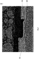
- Fig. 1 is a schematic structural view of a cross-sectional structure of the conventional semiconductor chip.
- the semiconductor chip 1' for example, a metal oxide semiconductor field effect transistor (MOSFET), cells of a gate (G) and a source (S) of the semiconductor chip 1' are periodically arranged, and are connected to a respective bonding pad (not shown) by metal.
- MOSFET metal oxide semiconductor field effect transistor
- a metal wiring connecting a plurality ofcells with of the gate G and the source S to a bonding pad and a metal of the bonding pad are collectively referred to as a metal wiring layer.
- the wiring connecting the cell of the gate G to the bonding pad generally includes such two forms as a heavily doped polysilicon and an additional metal layer on the polysilicon, which will not be described any more. And there is an interval between the gate G and the source S to provide the respective electrodes independently.
- the metal wiring layer may melt, flow and diffuse to form a metal connecting portion M. Therefore, the molten metal spans over the interval and connects to the gate G and the source S, which causes short circuit between the gate G and the source S, and thus the semiconductor chip 1' is switched off.
- the metal wiring layer that has been molten and solidified still makes the gate G and the source S short such that the semiconductor chip 1' cannot work normally, and on the other hand, before the high temperature fault occurs, the metal wiring layer itself is not directly connected to the gate G and the source S, but connect to the gate G and the source S due to the accidental diffusion after the metal wiring layer is molten, which is not controllable.
- An object of the present disclosure is to provide a semiconductor chip to enhance utility of the semiconductor chip.
- an embodiment of the present disclosure provides a semiconductor chip, which includes a functional area, a first end, a second end, a third end, and a connecting portion.
- the functional area has first and second sides opposite to each other.
- the first end is disposed on the first side.
- the third end is disposed on the first side, wherein the semiconductor chip is switched on or off according to a drive signal received between the third end and the first end.
- the connecting portion is disposed on the first side of the functional area and connected to the first end and the third end, wherein when the temperature rises above a first temperature, the connecting portion is in a conductive state, so that the semiconductor chip is switched off due to a short circuit between the first end and the third end; and when the temperature drops to be not higher than a third temperature, the connecting portion is in an insulating state, wherein the first temperature is higher than or equal to the third temperature.
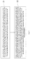
- a step S1 is performed, providing a chip body that includes a functional area, a first end, a second end, and a third end.
- the functional area has first and second sides opposite to each other, wherein the first end and the third end are disposed on the first side, and a drive signal is received between the first end and the third end to control the semiconductor chip to be switched on or off.
- a step S2 is performed, forming a connecting portion on the first side of the functional area and connecting the first end and the third end, wherein when a temperature of the connecting portion rises above a first temperature, the connecting portion is in a conductive state, so that the semiconductor chip is switched off due to a short circuit between the first end and the third end, and when the temperature of the connecting portion drops to be not higher than a third temperature, the connecting portion is in an insulating state, wherein the first temperature is higher than or equal to the third temperature.
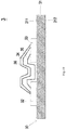
- Fig. 2 is a schematic view of a cross-sectional structure of a semiconductor chip of a first embodiment of the present disclosure
- Fig. 3 is a schematic diagram showing changes in resistivity of a connecting portion of the semiconductor chip as shown in Fig. 2 at different temperatures.
- the semiconductor chip 1 of the present disclosure is, for example but not limited to, a metal oxide semiconductor field effect transistor (MOSFET), an insulated gate bipolar transistor (IGBT), a high electron mobility transistor (HEMT) or a bipolar junction transistor (BJT), and includes a functional area 11, a first end 12, a second end (not shown), a third end 13 and a connecting portion 14.
- a material of the semiconductor chip 1 may be, but not limited to, silicon (Si), silicon carbide (SiC), gallium nitride (GaN), or the like.
- Functional area 11 includes a first side 111 and a second side 112 opposite to each other.
- the first end 12 is disposed on the first side 111.
- the first end 12 may be an output end, such as a source of a MOSFET.
- the functional area 11 is a semiconductor material area of the semiconductor chip 1, such as a Si material area of a Si-based device.
- the second end is an output end, such as a drain of a MOSFET.
- the third end 13 is disposed on the first side.
- the third end 13 is, for example, an input end, such as the gate of a MOSFET.
- the semiconductor chip 1 is switched on or off according to a drive signal received between the third end 13 and the first end 12, wherein the drive signal may be voltage or current.
- the functional area 11, the first end 12, the second end, and the third end 13 may constitute a chip body 10.
- the connecting portion 14 is disposed on the first side 111 of the functional area 11 and is connected to the first end 12 and the third end 13. Referring to Fig. 3 , when the ambient temperature of the connecting portion 14 shifts from one temperature to a new temperature because of system failure, chip failure, environmental change, etc, the temperature of the connecting portion 14 gradually becomes the new ambient temperature due to the thermal hysteresis phenomenon.
- the connecting portion 14 is vanadium dioxide (of VO 2 ).
- the resistivity of the connecting portion 14 When the temperature of the connecting portion 14 rises to a first temperature, the resistivity of the connecting portion 14 is lowered to be in a conductive state, such that the semiconductor chip 1 is switched off due to a short circuit between the first end 12 and the third end 13, which helps to prevent the temperature of the semiconductor chip from further rising to cause damage.
- the temperature of the connecting portion 14 drops to a third temperature, the resistivity of the connecting portion 14 rises to be in an insulating state, at this time, the semiconductor chip 1 may be restored to normal operation, wherein the first temperature is higher than or equal to the third temperature.
- the semiconductor chip 1 in the event that the first temperature is equal to the third temperature, when the temperature of the connecting portion 14 drops to not higher than the first temperature, the semiconductor chip 1 is in normal operation.
- the semiconductor chip 1 When the temperature of the connecting portion 14 rises above the first temperature to be in the conductive state, the semiconductor chip 1 is switched off due to the short circuit between the first end 12 and the third end 13.
- the connecting portion 14 When the temperature of the connecting portion 14 is lowered from a temperature higher than the first temperature to a temperature not higher than the first temperature, the connecting portion 14 changes from the conductive state to the insulating state.
- the value of the first temperature and the third temperature may be related to factors such as material producing process of the connecting portion 14, material thickness of the connecting portion 14, and speed of temperature variation of the connecting portion 14 and so on.
- the connecting portion 14 may be, but not limited to, temperature induced phase change materials, such as vanadium dioxide (VO 2 ), vanadium dioxide doped with germanium or other elements, and other temperature induced phase change materials.
- the connecting portion 14 can also be a glass with low melting temperature, such as vanadate material, phosphate material, borate material or silicate material or the like.
- the connecting portion made of glass with low melting temperature may be, but not limited to lead oxide - zinc oxide - diboron trioxide material systems (PbO-ZnO-B 2 O 3 ), lead oxide - aluminum oxide - diboron trioxide material system (PbO-Al 2 O 3 -B 2 O 3 ), lead oxide - bismuth trioxide - diboron trioxide material systems (PbO -Bi 2 O 3 -B 2 O 3 ), lead oxide - diboron trioxide - silicon dioxide material system (PbO-B 2 O 3 -SiO 2 ), potassium oxide - lead - silicon dioxide material system (K 2 O-Pb-SiO 2 ), zinc oxide - diboron trioxide - silicon dioxide material system (ZnO-B 2 O 3 -SiO 2 ), lead oxide - silicon dioxide - zinc oxide - barium oxide material system (PbO-SiO 2 -ZnO-BaO), sodium oxide - barium
- the first temperature is equal to the third temperature.
- the connecting portion 14 When the temperature of the connecting portion 14 rises to the temperature higher than the first temperature, the connecting portion 14 is in conductive state, and when the temperature of the connecting portion 14 drops to a temperature not higher than the first temperature, the connecting portion 14 is in insulating state.
- the semiconductor chip 1 of the present disclosure can be automatically switched off at a high temperature to avoid further damage, and can be restored to work normally after returning to the normal temperature.
- the semiconductor chip 1 of the present disclosure has a high practicability.
- the semiconductor chip 1 includes a bonding pad and a metal wiring layer (not shown).
- the first temperature is lower than a melting temperature of the metal wiring layer (for example, the melting point of aluminum is 660 °C), and the first temperature is less than a lowest temperature at which the semiconductor chip loses semiconductor characteristics. Therefore, when the state of the connecting portion 14 changes according to the boundary of the first temperature, the metal wiring layer and the characteristics of the semiconductor chip are not affected.
- a second temperature which is a maximum allowable junction temperature of the semiconductor chip 1 (in particular, the maximum allowable junction temperature refers to a given temperature under comprehensive consideration of performance, service life, etc, the temperature is generally lower than a limiting temperature that the semiconductor can withstand to remain the semiconductor switching characteristics).
- the semiconductor chip 1 can work normally when the temperature of the semiconductor chip 1 falls below the second temperature.
- the second temperature is lower than the first temperature
- the semiconductor chip 1 works normally that is, when the temperature of the semiconductor chip 1 drops to no higher than the second temperature
- the connecting portion 14 is in an insulating state.
- the maximum junction temperature, the minimum temperature for losing the semiconductor characteristics and a range of the first temperature are shown with different material types of semiconductor chips 1, which are not limited thereto.
- the semiconductor chip 1 may further include a first passivation layer 15, but the disclosure is not limited thereto.
- the first passivation layer 15 is disposed on the first side 111 of the functional area 11 for protecting the functional area 11.
- the connecting portion 14 covers the first passivation layer 15, wherein the material of the first passivation layer 15 may be but not limited to silicon dioxide (SiO 2 ), silicon nitride (SiN) or polyimide (PI).
- the first passivation layer 15 may be a composite layer such as a polyimide layer provided on silicon nitride, a silicon nitride layer composited on silicon dioxide, or the like.
- the moisture and pollution is blocked out of the first side 111 of the functional area 11 between the first end 12 and the third end 13 by the first passivation layer 15, thus there is a relatively low requirement for the material of the connecting portion 14 to block moisture and pollution so that the structure of the semiconductor chip 1 is relatively easy to be implemented and the manufacturing method is relatively simple.
- the first end 12 includes a plurality of first bonding pad 121
- the third end 13 includes a second bonding pad 131 and a second interconnect line 132.
- the connecting portion 14 may completely fill in a gap between the first end 12 and the third end 13 on the first side 111 of the functional area 11. As shown in Fig. 4 , the connecting portion 14 completely fills in an interval between the first bonding pad 121 and the second bonding pad 131 and an interval between the first bonding pad 121 and the second interconnect line 132. Therefore when the temperature at any location of the semiconductor chip 1 rises to higher than the first temperature, the connecting portion 14 is transitioned to the conductive state, and thus, sensitivity of the state transition of the semiconductor chip 1 is higher.
- the first end 12 includes a plurality of first bonding pad 121
- the third end 13 includes a second bonding pad 131 and a second interconnect line 132.
- the connecting portion 14 may only partly fill in a gap between the first end 12 and the third end 13 on the first side 111 of the functional area 11.
- the connecting portion 14 fills in a location of the semiconductor chip 1 with higher temperature than other areas.
- the connecting portion 14 partly fills in a gap between the first bonding pad 121 and the second bonding pad 131 and a gap between the first bonding pad 121 and the second interconnect line 132, so that one or more connecting portions 14 can be flexibly disposed to reduce cost of the semiconductor chip 1.
- the second end of the semiconductor chip is disposed on the second side 112 of the functional area 11.
- the first end 12 includes a first bonding pad 121 and the first interconnect line 122
- the third end 13 includes a second bonding pad 131 and a second interconnect line 132
- the connecting portion 14 only partially fills in a gap between the first end 12 and the third end 13 on the first side 111 of the functional area 11, as shown in Fig. 6 .
- the connecting portion 14 partly fills in a gap between the first bonding pad 121 and the second interconnect line and a gap between the first interconnect line 122 and the second interconnect line 132.
- the second end 19 of the semiconductor chip is disposed on the first side 111 of the functional area 11.
- a schematic view of a cross-sectional structure of a semiconductor chip of a second embodiment of the present disclosure is shown.
- a first passivation layer 15 is disposed on the first side 111 of the functional area 11, and at least partly covers the first end 12 and a third end 13.
- the connecting portion 14 is formed on the first side 111 of the functional area 11 with a physical vapor deposition, a chemical vapor deposition, spin-on glass, printing or dot coating process, thereby forming the semiconductor chip 1, and the connecting portion 14 covers the first passivation layer 15.
- Fig. 8 a schematic view of a cross-sectional structure of a semiconductor chip of a third embodiment of the present disclosure is shown.
- the semiconductor chip is firstly disposed on a package structure D, and then the connecting portion 14 is provided.
- the connecting portion 14 is formed on the first side 111 of the functional area 11 by processes, such as dot coating or printing, and the connecting portion 14 covers the first passivation layer 15.
- the connecting portion 14 of the semiconductor chip 1 of the present disclosure can be provided in a front end chip process or a back end packaging process, and the connecting portion 14 may be disposed after the first passivation layer 15 is disposed.
- the process for manufacturing the semiconductor chip 1 of the present disclosure is flexible, and difficulty of the process can be reduced.
- the semiconductor chip 2 of the present embodiment includes a functional area 21, a first end 22, a third end 23, a connecting portion 24, and a second passivation layer 25, wherein the functional area 21 and the first end 22, the third end 23, and the connecting portion 24 of the semiconductor chip 2 are similar to the functional area 11, the first end 12, the third end 13, and the connecting portion 14 of the semiconductor chip 1 as shown in Fig. 2 , respectively. Structure, actuation and function of the similar components will not be repeated here.
- Fig. 2 in the embodiment shown in Fig.
- the connecting portion 24 of the semiconductor chip 2 is provided on the first side 211 of the functional area 21, and the second passivation layer 25 covers the connecting portion 24 to protect the connecting portion 24.
- the material or the like of the second passivation layer 25 may be the same as that of the first passivation layer 15.
- the semiconductor chip 3 of the present embodiment includes a functional area 31, a first end 32, a third end 33, a connecting portion 34, and a first passivation layer 35, wherein the functional area 31, the first end 32, the third end 33, the connecting portion 34 and the first passivation layer 35 of the semiconductor chip 3 are similar to the functional area 11, the first end 12, the third end 13, the connecting portion 14 and the first passivation layer 15 of the semiconductor chip 1 as shown in Fig. 2 , respectively. Structure, actuation and function of similar components will not be repeated here. Compared to the embodiment illustrated in Fig.
- the semiconductor chip 3 further includes a second passivation layer 36, and the second passivation layer 36 covers the connecting portion 34 in order to protect the functional area 31 and the connecting portion 34, so that the semiconductor chip 3 may have a better protection capability.
- the first passivation layer 35 may be, but not limited to, silicon dioxide (SiO 2 )
- the second passivation layer 36 may be, but not limited to, polyimide (PI).
- the second passivation layer 36 is composed of a composite material, such as a composite layer of ethyl silicate (TEOS) and silicon nitride (SiN) having a good shape and a stress relief.
- TEOS ethyl silicate
- SiN silicon nitride
- the semiconductor chip 4 of the present embodiment includes a functional area 41, a first end 42, a third end 43, a connecting portion 44, and a first passivation layer 45, wherein the functional area 41, the first end 42, the third end 43, the connecting portion 44 and the first passivation layer 45 of the semiconductor chip 4 are similar to the functional area 11, the first end 12, the third end 13, the connecting portion 14 and the first passivation layer 15 of the semiconductor chip 1 shown in Fig. 2 , respectively. Structure, actuation and function of the similar components will not be repeated here. Compared to the embodiment illustrated in Fig.
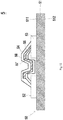
- the semiconductor chip 4 further includes a second passivation layer 46 and a metal layer 47.
- the second passivation layer 46 covers the connecting portion 44 to protect the functional area 41 and the connecting portion 44, so that the semiconductor chip 4 may have a better protection capability.
- the metal layer 47 is disposed between the connecting portion 44 and the second passivation layer 46 and is in contact with the connecting portion 44. The metal layer 47 is not directly connected to the first end 42 and the third end 43 but connected to the first end 42 and the third end 43 through the connecting portion 44, such that the impedance between the first end 42 and the third end 43 is reduced.
- the first passivation layer 45 may be, but not limited to, silicon dioxide (SiO 2)
- the second passivation layer 46 may be, but not limited to, polyimide (PI).
- the second passivation layer 46 is composed of composite materials, such as a composite layer of ethyl silicate (TEOS) and silicon nitride (SiN) with a good shape and a stress relief.
- the metal layer 47 can be formed by physical vapor deposition (PVD).
- PVD physical vapor deposition
- the semiconductor chip 5 of the present embodiment includes a functional area 51, a first end 52, the third end 53, a connecting portion 54 and a first passivation layer 55, wherein the functional area 51, the first end 52, the third end 53, the connecting portion 54 and the first passivation layer 55 of the semiconductor chip 5 are similar to the functional area 11, the first end 12, the third end 13, the connecting portion 14 and the first passivation layer 15 of the semiconductor chip 1 shown in Fig. 2 , respectively. Structure, actuation and function of the similar components will not be repeated here. Compared to the embodiment illustrated in Fig.
- a semiconductor chip 5 further includes a second passivation layer 56 and a metal layer 57.
- the second passivation layer 56 covers the connecting portion 54 to protect the functional area 51 and the connecting portion 54 so that the semiconductor chip 5 may have a better protection capability.
- the metal layer 57 is disposed between the connecting portion 54 and the second passivation layer 56 and is in contact with the connecting portion 54. In this embodiment, one end of the metal layer 57 is connected to the third end 53, and the other end of the metal layer 57 is connected to the first end 52 via the connecting portion, such that the impedance between the first end 52 and the third end 53 is reduced.
- the short circuit can be achieved more quickly, and thus, the semiconductor chip 5 may be switched off more quickly.
- one end of the metal layer 57 is connected to the first end 52, and the other end of the metal layer 57 is connected to the third portion 53 via the connecting portion 54, such that the impedance between the first end 52 and the third end 53 is also reduced, and thus the semiconductor chip 5 is switched off more quickly.
- the end of the metal layer may be located at any place of the connecting portion.
- the first passivation layer 55 may be, but not limited to, silicon dioxide (SiO 2 ), and the second passivation layer 56 may be, but not limited to, polyimide (PI).
- the second passivation layer 56 is composed of composite materials, such as a composite layer of ethyl silicate (TEOS) and silicon nitride (SiN) with good shape and stress relief.
- the metal layer 57 can be formed by physical vapor deposition (PVD).
- PVD physical vapor deposition
- the first passivation layer 55 and the second passivation layer 56 in this embodiment may be omitted separately or completely, and the present disclosure is not limited thereto.
- the metal layer in the embodiments of the present disclosure is disposed in contact with the connecting portion.
- the word contact here includes direct contact and indirect contact by other conductive materials, and partial contact is also allowable.
- the metal layer may be disposed between the connecting portion and the second passivation layer, or between the connecting portion and the first passivation layer, or both above. If the first passivation layer and/or the second passivation layer are omitted, a metal layer may also be provided to at least partially contact the connecting portion.
- the metal layer may also be divided into multiple sections and multiple layers, and the present disclosure is not limited thereto.
- the semiconductor chip 6 of this embodiment includes a functional area 61, first end 62, a third end 63 and a polysilicon 64, but a second end is not shown.
- the functional area 61, the first end 62 and the third end 63 of the semiconductor chip 6 are similar to the functional area 11, the first end 12 and the third end 13 of the semiconductor chip 1 as shown in Fig. 2 , respectively. Structure, actuation and function of the similar components will not be repeated here.
- Fig. 2 in the embodiment of Fig.
- insulating medium 70 is provided between the metal wirings connecting cells of the third end (e.g., gate of the MOSFET) and a first end (e.g., source of the MOSFET) of the semiconductor chip 6 such as a MOSFET.
- the connecting portion may be disposed inside the insulating medium 70 to connect the first end 62 and the third end 63 (e.g., gate of the MOSFET).
- the connecting portion may not be disposed in the insulating layer 70, but on the insulating layer 70, and disposed between the first end 62 and the third end 63. Since the insulating layer 70 is disposed on the first side 611 of the functional area 61, the connecting portion disposed on the insulating layer 70 is also considered to be disposed on the first side 611 of the functional area 61, which is not limited to direct contact or indirect contact.
- a step S1 is performed to set the chip body 10, which includes a functional area 11, a first end 12, a second end, and a third end 13.
- the functional area 11 has a first 111 and second sides 112 opposite to each other, and the first end 12 and the third end 13 are disposed on the first side 111.
- the drive signal is received between the first end 12 and the third end 13 to control the semiconductor chip 1 to be switched on or off.
- a step S2 is performed to form a connecting portion 14 on the first side 111 of the functional area 11 and connect the first end 12 and the third end 13.
- the connecting portion 14 When the temperature of the connecting portion 14 rises above the first temperature the connecting portion 14 is in a conductive state so that the semiconductor chip 1 is switched off due to the short circuit between the first end 12 and the third end 13. When the temperature of the connecting portion 14 drops to a temperature not higher than the third temperature, the connecting portion 14 is in an insulating state, wherein the first temperature is higher than or equal to the third temperature.
- the above method may also be applied to other embodiments of the present disclosure, and thus will not be described herein.
- the step S1 is performed to set the chip body 40, which includes a functional area 41, a first end 42, a second end, and a third end 43.
- the functional area 41 has a first side 411 and second side 412 opposite to each other, and the first end 42 and the third end 43 are disposed on the first side 411.
- the drive signal is received between the first end 42 and the third end 43 to control the semiconductor chip 1 to be switched on or off.
- the step S2 is performed to form a connecting portion 44 on the first side 411 of the functional area 41 and connects the first end 42 and the third end 43.
- the connecting portion 44 When the temperature of the connecting portion 44 rises above the first temperature, the connecting portion 44 is in a conductive state so that the semiconductor chip 1 is switched off due to a short circuit between the first end 42 and the third end 43. When the temperature of the connecting portion 44 drops to a temperature not higher than the third temperature, the connecting portion 44 is in an insulating state, wherein the first temperature is higher than or equal to the third temperature.
- a step S3 is performed to form the metal layer 47 in contact with the connecting portion 44 such that the metal layer 47 is connected to the first end 42 and the third end 43 via the connecting portion 44.
- one end of the metal layer 47 is in contact with the first end 42 and the other end of the metal layer 47 is connected to the third end 43 via the connecting portion 44, or one end of the metal layer 47 is in contact with the third end 43, and the other end of the metal layer 47 is connected to the first end 42 via the connecting portion 44.
- the end of the metal layer may be located at any place of connecting portion.
- the semiconductor chip of the present disclosure when the temperature of the connecting portion of the semiconductor chip of the present disclosure rises to be higher than the first temperature, the semiconductor chip is in a conductive state, and when the temperature of the connecting portion drops to no higher than the first temperature, the semiconductor chip is in an insulating state.
- the semiconductor chip of the present disclosure due to the state transformation of the connecting portion at different temperatures, may be automatically switched off at a high temperature to avoid further damage, and may be recovered after returning to the normal temperature, and thus the semiconductor chip of the present disclosure has a high practicability.
- the connecting portion is switched between the insulating state and the conductive state due to the material characteristics of the connecting portion itself, thus, it is safe and reliable to protect the semiconductor chip by being switched off at a high temperature and returning to a normal operation at a low temperature depending on the material characteristics.
Landscapes
- Semiconductor Integrated Circuits (AREA)
- Measuring Temperature Or Quantity Of Heat (AREA)
Abstract
Description
- This disclosure relates to a technical field of an integrated circuit, and in particular to a semiconductor chip with a temperature controlled connecting portion.
- With rapid development of new energy vehicles, computing equipments, autonomous driving, smart phones, requirements for power supply products for the above-mentioned fields are becoming higher and higher. A semiconductor chip is a key component for the power supply products and is widely used in switching converter circuits, power amplifier circuits, rectifier circuits and drive circuits, etc. Thus, requirement for reliability of the semiconductor chip is gradually increasing.
- Generally speaking, semiconductor chips suffer from a temperature rising progress before failure due to various reasons such as short circuit, overcurrent, abnormal heat dissipation or driving abnormality.
Fig. 1 is a schematic structural view of a cross-sectional structure of the conventional semiconductor chip. As shown inFig. 1 , the semiconductor chip 1', for example, a metal oxide semiconductor field effect transistor (MOSFET), cells of a gate (G) and a source (S) of the semiconductor chip 1' are periodically arranged, and are connected to a respective bonding pad (not shown) by metal. A metal wiring connecting a plurality ofcells with of the gate G and the source S to a bonding pad and a metal of the bonding pad are collectively referred to as a metal wiring layer. It should be particularly noted that the wiring connecting the cell of the gate G to the bonding pad generally includes such two forms as a heavily doped polysilicon and an additional metal layer on the polysilicon, which will not be described any more. And there is an interval between the gate G and the source S to provide the respective electrodes independently. When some faults occur, if the temperature of the chip rises, and the metal wiring layer may melt, flow and diffuse to form a metal connecting portion M. Therefore, the molten metal spans over the interval and connects to the gate G and the source S, which causes short circuit between the gate G and the source S, and thus the semiconductor chip 1' is switched off. However, although the semiconductor chip 1' is switched off due to molten of the metal wiring layer at a high temperature, on the one hand, after returning to the normal temperature, the metal wiring layer that has been molten and solidified still makes the gate G and the source S short such that the semiconductor chip 1' cannot work normally, and on the other hand, before the high temperature fault occurs, the metal wiring layer itself is not directly connected to the gate G and the source S, but connect to the gate G and the source S due to the accidental diffusion after the metal wiring layer is molten, which is not controllable. - As a result, how to develop a semiconductor chip to overcome the above disadvantages is an urgent need at present.
- An object of the present disclosure is to provide a semiconductor chip to enhance utility of the semiconductor chip.
- To achieve the above object, an embodiment of the present disclosure provides a semiconductor chip, which includes a functional area, a first end, a second end, a third end, and a connecting portion. The functional area has first and second sides opposite to each other. The first end is disposed on the first side. The third end is disposed on the first side, wherein the semiconductor chip is switched on or off according to a drive signal received between the third end and the first end. The connecting portion is disposed on the first side of the functional area and connected to the first end and the third end, wherein when the temperature rises above a first temperature, the connecting portion is in a conductive state, so that the semiconductor chip is switched off due to a short circuit between the first end and the third end; and when the temperature drops to be not higher than a third temperature, the connecting portion is in an insulating state, wherein the first temperature is higher than or equal to the third temperature.
- To achieve the above object, another embodiment of the present disclosure provides a method used in a semiconductor chip. First, a step S1 is performed, providing a chip body that includes a functional area, a first end, a second end, and a third end. The functional area has first and second sides opposite to each other, wherein the first end and the third end are disposed on the first side, and a drive signal is received between the first end and the third end to control the semiconductor chip to be switched on or off. Next, a step S2 is performed, forming a connecting portion on the first side of the functional area and connecting the first end and the third end, wherein when a temperature of the connecting portion rises above a first temperature, the connecting portion is in a conductive state, so that the semiconductor chip is switched off due to a short circuit between the first end and the third end, and when the temperature of the connecting portion drops to be not higher than a third temperature, the connecting portion is in an insulating state, wherein the first temperature is higher than or equal to the third temperature.
-
-
Fig. 1 is a schematic structural view of a cross-sectional structure of a conventional semiconductor chip. -
Fig. 2 is a schematic structural view of a cross-sectional structure of a semiconductor chip of a first embodiment of the present disclosure. -
Fig. 3 is a schematic view showing changes in resistivity of a connecting portion of the semiconductor chip as shown inFig. 2 at different temperatures. -
Fig. 4 is a schematic top view of a structure of an embodiment of the semiconductor chip as shown inFig. 2 . -
Fig. 5 is a schematic top view of a structure of another embodiment of the semiconductor chip as shown inFig. 2 . -
Fig. 6 is a schematic structural top view of a further embodiment of the semiconductor chip as shown inFig. 2 . -
Fig. 7 is a schematic view of a cross-sectional structure of a semiconductor chip of a second embodiment of the present disclosure. -
Fig. 8 is a schematic view of a cross-sectional structure of a semiconductor chip of a third embodiment of the present disclosure. -
Fig. 9 is a schematic view of a cross-sectional structure of a semiconductor chip of a fourth embodiment of the present disclosure. -
Fig. 10 is a schematic view of a cross-sectional structure of a semiconductor chip of a fifth embodiment of the present disclosure. -
Fig. 11 is a schematic view of a cross-sectional structure of a semiconductor chip of a sixth embodiment of the present disclosure. -
Fig. 12 is a schematic view of a cross-sectional structure of a semiconductor chip of a seventh embodiment of the present disclosure. -
Fig. 13 is a schematic view of a cross-sectional structure of a semiconductor chip of an eighth embodiment of the present disclosure. -
Fig. 14 is a schematic flow chart of a method of the semiconductor chip as shown inFig. 2 . -
Fig. 15 is a schematic flow chart of a method of the semiconductor chip as shown inFig. 11 . - Reference numbers are listed as follows:
- 1': semiconductor chip
- G: gate
- S: source
- M: metal connecting portion
- 1, 2, 3, 4, 5, 6: semiconductor chip
- 10, 20, 30, 40, 50, 60: chip body
- 11, 21, 31, 41, 51, 61: functional area
- 111, 211, 311, 411, 511, 611: first side
- 112, 212, 312, 412, 512, 612: second side
- 12, 22, 32, 42, 52, 62: first end
- 13, 23, 33, 43, 53, 63: third end
- 64: polysilicon
- 70: insulating medium
- 15, 35, 45, 55: first passivation layer
- 25, 36, 46, 56: second passivation layer
- 47, 57: metal layer
- D: package structure
- 19: second end
- S1∼S3: steps
- Typical embodiments embodying features and advantages of this disclosure will be set forth below in detail. It should be understood that various modifications may be made in different embodiments without departing from the scope of this disclosure, wherein the specification and drawings in essential are used for description but not limit to this disclosure..
- Referring to
Figs. 2 and3 , in whichFig. 2 is a schematic view of a cross-sectional structure of a semiconductor chip of a first embodiment of the present disclosure, andFig. 3 is a schematic diagram showing changes in resistivity of a connecting portion of the semiconductor chip as shown inFig. 2 at different temperatures. As shown in the figures, thesemiconductor chip 1 of the present disclosure is, for example but not limited to, a metal oxide semiconductor field effect transistor (MOSFET), an insulated gate bipolar transistor (IGBT), a high electron mobility transistor (HEMT) or a bipolar junction transistor (BJT), and includes afunctional area 11, afirst end 12, a second end (not shown), athird end 13 and a connectingportion 14. In some embodiments, a material of thesemiconductor chip 1 may be, but not limited to, silicon (Si), silicon carbide (SiC), gallium nitride (GaN), or the like. -
Functional area 11 includes afirst side 111 and asecond side 112 opposite to each other. Thefirst end 12 is disposed on thefirst side 111. Thefirst end 12 may be an output end, such as a source of a MOSFET. Thefunctional area 11 is a semiconductor material area of thesemiconductor chip 1, such as a Si material area of a Si-based device. The second end is an output end, such as a drain of a MOSFET. Thethird end 13 is disposed on the first side. Thethird end 13 is, for example, an input end, such as the gate of a MOSFET. Thesemiconductor chip 1 is switched on or off according to a drive signal received between thethird end 13 and thefirst end 12, wherein the drive signal may be voltage or current. In some embodiments, thefunctional area 11, thefirst end 12, the second end, and thethird end 13 may constitute achip body 10. The connectingportion 14 is disposed on thefirst side 111 of thefunctional area 11 and is connected to thefirst end 12 and thethird end 13. Referring toFig. 3 , when the ambient temperature of the connectingportion 14 shifts from one temperature to a new temperature because of system failure, chip failure, environmental change, etc, the temperature of the connectingportion 14 gradually becomes the new ambient temperature due to the thermal hysteresis phenomenon. For example, the connectingportion 14 is vanadium dioxide (of VO2). When the temperature of the connectingportion 14 rises to a first temperature, the resistivity of the connectingportion 14 is lowered to be in a conductive state, such that thesemiconductor chip 1 is switched off due to a short circuit between thefirst end 12 and thethird end 13, which helps to prevent the temperature of the semiconductor chip from further rising to cause damage. In addition, when the temperature of the connectingportion 14 drops to a third temperature, the resistivity of the connectingportion 14 rises to be in an insulating state, at this time, thesemiconductor chip 1 may be restored to normal operation, wherein the first temperature is higher than or equal to the third temperature. In some embodiments, in the event that the first temperature is equal to the third temperature, when the temperature of the connectingportion 14 drops to not higher than the first temperature, thesemiconductor chip 1 is in normal operation. When the temperature of the connectingportion 14 rises above the first temperature to be in the conductive state, thesemiconductor chip 1 is switched off due to the short circuit between thefirst end 12 and thethird end 13. When the temperature of the connectingportion 14 is lowered from a temperature higher than the first temperature to a temperature not higher than the first temperature, the connectingportion 14 changes from the conductive state to the insulating state. In some of the above embodiments, the value of the first temperature and the third temperature may be related to factors such as material producing process of the connectingportion 14, material thickness of the connectingportion 14, and speed of temperature variation of the connectingportion 14 and so on. - In some embodiments, the connecting
portion 14 may be, but not limited to, temperature induced phase change materials, such as vanadium dioxide (VO2), vanadium dioxide doped with germanium or other elements, and other temperature induced phase change materials. The connectingportion 14 can also be a glass with low melting temperature, such as vanadate material, phosphate material, borate material or silicate material or the like. The connecting portion made of glass with low melting temperature may be, but not limited to lead oxide - zinc oxide - diboron trioxide material systems (PbO-ZnO-B2O3), lead oxide - aluminum oxide - diboron trioxide material system (PbO-Al2O3-B2O3), lead oxide - bismuth trioxide - diboron trioxide material systems (PbO -Bi2O3-B2O3), lead oxide - diboron trioxide - silicon dioxide material system (PbO-B2O3-SiO2), potassium oxide - lead - silicon dioxide material system (K2O-Pb-SiO2), zinc oxide - diboron trioxide - silicon dioxide material system (ZnO-B2O3-SiO2), lead oxide - silicon dioxide - zinc oxide - barium oxide material system (PbO-SiO2-ZnO-BaO), sodium oxide - barium oxide - silicon dioxide material system (Na2O-BaO-SiO2), zinc oxide - diboron trioxide - phosphorus pentoxide material systems (ZnO-B2O3-P2O5), lithium oxide - aluminum oxide - silicon dioxide material system (Li2O-Al2O3-SiO2), thallium oxide - vanadium pentoxide - tellurium oxide - arsenic oxide material systems (Tl2O-V2O5-TeO2-AsO3), bismuth oxide - diboron trioxide material systems (Bi2O3-B2O3), lead oxide - vanadium pentoxide - bismuth oxide - zinc oxide system material (PbO-V2O5-Bi2O3-ZnO), lithium oxide - zinc oxide - silicon dioxide material system (Li2O-ZnO -SiO2), tin oxide - zinc oxide - phosphorus pentoxide material systems (SnO-ZnO-P2O5), vanadium pentoxide - phosphorus pentoxide - antimony oxide material system (V2O5-P2O5-SbO), etc. In addition, more other materials may be added to the above material to adjust the melting point, strength, thermal expansion coefficient, wettability, electrical properties and manufacturability. - It can be seen from the above description that when the above mentioned material is used for the connecting
portion 14, the first temperature is equal to the third temperature. When the temperature of the connectingportion 14 rises to the temperature higher than the first temperature, the connectingportion 14 is in conductive state, and when the temperature of the connectingportion 14 drops to a temperature not higher than the first temperature, the connectingportion 14 is in insulating state. Thus, compared to the conventional semiconductor chip 1' that cannot work normally after returning to the normal temperature, thesemiconductor chip 1 of the present disclosure can be automatically switched off at a high temperature to avoid further damage, and can be restored to work normally after returning to the normal temperature. Thus, thesemiconductor chip 1 of the present disclosure has a high practicability. - In this embodiment, the
semiconductor chip 1 includes a bonding pad and a metal wiring layer (not shown). The first temperature is lower than a melting temperature of the metal wiring layer (for example, the melting point of aluminum is 660 °C), and the first temperature is less than a lowest temperature at which the semiconductor chip loses semiconductor characteristics. Therefore, when the state of the connectingportion 14 changes according to the boundary of the first temperature, the metal wiring layer and the characteristics of the semiconductor chip are not affected. In addition, there is a second temperature, which is a maximum allowable junction temperature of the semiconductor chip 1 (in particular, the maximum allowable junction temperature refers to a given temperature under comprehensive consideration of performance, service life, etc, the temperature is generally lower than a limiting temperature that the semiconductor can withstand to remain the semiconductor switching characteristics). Therefore, thesemiconductor chip 1 can work normally when the temperature of thesemiconductor chip 1 falls below the second temperature. As the second temperature is lower than the first temperature, when thesemiconductor chip 1 works normally, that is, when the temperature of thesemiconductor chip 1 drops to no higher than the second temperature, the connectingportion 14 is in an insulating state. Thus a short circuit between the two control electrodes (thefirst end 12 and the third end 13) can be avoided. In table 1 below, the maximum junction temperature, the minimum temperature for losing the semiconductor characteristics and a range of the first temperature are shown with different material types ofsemiconductor chips 1, which are not limited thereto.Table 1 material of semiconductor chip maximum junction temperature (°C) minimum temperature for losing semiconductor characteristics (°C) range of first temperature (°C) Si ∼150-175 < 200 ∼175-200 GaN ∼175-200 > 600 ∼260-600 SiC ∼175-200 > 600 ∼260-600 - Continue to refer to
Fig. 2 , thesemiconductor chip 1 may further include afirst passivation layer 15, but the disclosure is not limited thereto. Thefirst passivation layer 15 is disposed on thefirst side 111 of thefunctional area 11 for protecting the functional area 11.The connectingportion 14 covers thefirst passivation layer 15, wherein the material of thefirst passivation layer 15 may be but not limited to silicon dioxide (SiO2), silicon nitride (SiN) or polyimide (PI). Further, thefirst passivation layer 15 may be a composite layer such as a polyimide layer provided on silicon nitride, a silicon nitride layer composited on silicon dioxide, or the like. In this embodiment, the moisture and pollution is blocked out of thefirst side 111 of thefunctional area 11 between thefirst end 12 and thethird end 13 by thefirst passivation layer 15, thus there is a relatively low requirement for the material of the connectingportion 14 to block moisture and pollution so that the structure of thesemiconductor chip 1 is relatively easy to be implemented and the manufacturing method is relatively simple. - In some embodiments, the
first end 12 includes a plurality offirst bonding pad 121, and thethird end 13 includes asecond bonding pad 131 and asecond interconnect line 132. The connectingportion 14 may completely fill in a gap between thefirst end 12 and thethird end 13 on thefirst side 111 of thefunctional area 11. As shown inFig. 4 , the connectingportion 14 completely fills in an interval between thefirst bonding pad 121 and thesecond bonding pad 131 and an interval between thefirst bonding pad 121 and thesecond interconnect line 132. Therefore when the temperature at any location of thesemiconductor chip 1 rises to higher than the first temperature, the connectingportion 14 is transitioned to the conductive state, and thus, sensitivity of the state transition of thesemiconductor chip 1 is higher. - In some other embodiments, the
first end 12 includes a plurality offirst bonding pad 121, and thethird end 13 includes asecond bonding pad 131 and asecond interconnect line 132. The connectingportion 14 may only partly fill in a gap between thefirst end 12 and thethird end 13 on thefirst side 111 of thefunctional area 11. For example, the connectingportion 14 fills in a location of thesemiconductor chip 1 with higher temperature than other areas. As shown inFig. 5 , the connectingportion 14 partly fills in a gap between thefirst bonding pad 121 and thesecond bonding pad 131 and a gap between thefirst bonding pad 121 and thesecond interconnect line 132, so that one or more connectingportions 14 can be flexibly disposed to reduce cost of thesemiconductor chip 1. In some embodiments, as shown inFigs. 4 and5 , the second end of the semiconductor chip is disposed on thesecond side 112 of thefunctional area 11. - In some embodiments, the
first end 12 includes afirst bonding pad 121 and thefirst interconnect line 122, and thethird end 13 includes asecond bonding pad 131 and asecond interconnect line 132, and the connectingportion 14 only partially fills in a gap between thefirst end 12 and thethird end 13 on thefirst side 111 of thefunctional area 11, as shown inFig. 6 . The connectingportion 14 partly fills in a gap between thefirst bonding pad 121 and the second interconnect line and a gap between thefirst interconnect line 122 and thesecond interconnect line 132. In some embodiments, as shown inFig. 6 , thesecond end 19 of the semiconductor chip is disposed on thefirst side 111 of thefunctional area 11. - Referring to
Fig. 7 , a schematic view of a cross-sectional structure of a semiconductor chip of a second embodiment of the present disclosure is shown. In this embodiment, afirst passivation layer 15 is disposed on thefirst side 111 of thefunctional area 11, and at least partly covers thefirst end 12 and athird end 13. The connectingportion 14 is formed on thefirst side 111 of thefunctional area 11 with a physical vapor deposition, a chemical vapor deposition, spin-on glass, printing or dot coating process, thereby forming thesemiconductor chip 1, and the connectingportion 14 covers thefirst passivation layer 15. Referring toFig. 8 , a schematic view of a cross-sectional structure of a semiconductor chip of a third embodiment of the present disclosure is shown. In this embodiment, the semiconductor chip is firstly disposed on a package structure D, and then the connectingportion 14 is provided. The connectingportion 14 is formed on thefirst side 111 of thefunctional area 11 by processes, such as dot coating or printing, and the connectingportion 14 covers thefirst passivation layer 15. As can be seen, the connectingportion 14 of thesemiconductor chip 1 of the present disclosure can be provided in a front end chip process or a back end packaging process, and the connectingportion 14 may be disposed after thefirst passivation layer 15 is disposed. Thus, the process for manufacturing thesemiconductor chip 1 of the present disclosure is flexible, and difficulty of the process can be reduced. - Referring to
Fig. 9 , a schematic view of a cross-sectional structure of a semiconductor chip of a fourth embodiment of the present disclosure is shown. As shown in the figure, thesemiconductor chip 2 of the present embodiment includes afunctional area 21, afirst end 22, athird end 23, a connectingportion 24, and asecond passivation layer 25, wherein thefunctional area 21 and thefirst end 22, thethird end 23, and the connectingportion 24 of thesemiconductor chip 2 are similar to thefunctional area 11, thefirst end 12, thethird end 13, and the connectingportion 14 of thesemiconductor chip 1 as shown inFig. 2 , respectively. Structure, actuation and function of the similar components will not be repeated here. Compared to the embodiment illustrated inFig. 2 , in the embodiment shown inFig. 9 , the connectingportion 24 of thesemiconductor chip 2 is provided on thefirst side 211 of thefunctional area 21, and thesecond passivation layer 25 covers the connectingportion 24 to protect the connectingportion 24. The material or the like of thesecond passivation layer 25 may be the same as that of thefirst passivation layer 15. - Referring to
Fig. 10 , a schematic view of a cross-sectional structure of a semiconductor chip of a fifth embodiment of the present disclosure is shown. As shown in the figure, thesemiconductor chip 3 of the present embodiment includes afunctional area 31, afirst end 32, athird end 33, a connectingportion 34, and afirst passivation layer 35, wherein thefunctional area 31, thefirst end 32, thethird end 33, the connectingportion 34 and thefirst passivation layer 35 of thesemiconductor chip 3 are similar to thefunctional area 11, thefirst end 12, thethird end 13, the connectingportion 14 and thefirst passivation layer 15 of thesemiconductor chip 1 as shown inFig. 2 , respectively. Structure, actuation and function of similar components will not be repeated here. Compared to the embodiment illustrated inFig. 2 , in the embodiment shown inFig. 10 , thesemiconductor chip 3 further includes asecond passivation layer 36, and thesecond passivation layer 36 covers the connectingportion 34 in order to protect thefunctional area 31 and the connectingportion 34, so that thesemiconductor chip 3 may have a better protection capability. In some embodiments, thefirst passivation layer 35 may be, but not limited to, silicon dioxide (SiO2), and thesecond passivation layer 36 may be, but not limited to, polyimide (PI). In other embodiments, thesecond passivation layer 36 is composed of a composite material, such as a composite layer of ethyl silicate (TEOS) and silicon nitride (SiN) having a good shape and a stress relief. - Referring to
Fig. 11 , a schematic view of a cross-sectional structure of a semiconductor chip of a sixth embodiment of the present disclosure is shown. As shown in the figure, thesemiconductor chip 4 of the present embodiment includes afunctional area 41, afirst end 42, athird end 43, a connectingportion 44, and afirst passivation layer 45, wherein thefunctional area 41, thefirst end 42, thethird end 43, the connectingportion 44 and thefirst passivation layer 45 of thesemiconductor chip 4 are similar to thefunctional area 11, thefirst end 12, thethird end 13, the connectingportion 14 and thefirst passivation layer 15 of thesemiconductor chip 1 shown inFig. 2 , respectively. Structure, actuation and function of the similar components will not be repeated here. Compared to the embodiment illustrated inFig. 2 , in the embodiment shown inFig. 11 , thesemiconductor chip 4 further includes asecond passivation layer 46 and ametal layer 47. Thesecond passivation layer 46 covers the connectingportion 44 to protect thefunctional area 41 and the connectingportion 44, so that thesemiconductor chip 4 may have a better protection capability. Themetal layer 47 is disposed between the connectingportion 44 and thesecond passivation layer 46 and is in contact with the connectingportion 44. Themetal layer 47 is not directly connected to thefirst end 42 and thethird end 43 but connected to thefirst end 42 and thethird end 43 through the connectingportion 44, such that the impedance between thefirst end 42 and thethird end 43 is reduced. Thus, when the temperature of the connectingportion 44 rises to higher than the first temperature and the connectingportion 44 is in a conductive state, the short circuit can be achieved more quickly. Thus, thesemiconductor chip 4 can be switched off more quickly. In some embodiments, thefirst passivation layer 45 may be, but not limited to, silicon dioxide (SiO 2), and thesecond passivation layer 46 may be, but not limited to, polyimide (PI). In other embodiments, thesecond passivation layer 46 is composed of composite materials, such as a composite layer of ethyl silicate (TEOS) and silicon nitride (SiN) with a good shape and a stress relief. In some embodiments, themetal layer 47 can be formed by physical vapor deposition (PVD). Thefirst passivation layer 45 and thesecond passivation layer 46 in this embodiment may be omitted separately or completely, and the present disclosure is not limited thereto. - Referring to
Fig. 12 , a schematic view of a cross-sectional structure of a semiconductor chip of a seventh embodiment of the present disclosure is shown. As shown in the figure, thesemiconductor chip 5 of the present embodiment includes afunctional area 51, afirst end 52, thethird end 53, a connectingportion 54 and afirst passivation layer 55, wherein thefunctional area 51, thefirst end 52, thethird end 53, the connectingportion 54 and thefirst passivation layer 55 of thesemiconductor chip 5 are similar to thefunctional area 11, thefirst end 12, thethird end 13, the connectingportion 14 and thefirst passivation layer 15 of thesemiconductor chip 1 shown inFig. 2 , respectively. Structure, actuation and function of the similar components will not be repeated here. Compared to the embodiment illustrated inFig. 2 , in the embodiment shown inFig. 12 , asemiconductor chip 5 further includes asecond passivation layer 56 and ametal layer 57. Thesecond passivation layer 56 covers the connectingportion 54 to protect thefunctional area 51 and the connectingportion 54 so that thesemiconductor chip 5 may have a better protection capability. Themetal layer 57 is disposed between the connectingportion 54 and thesecond passivation layer 56 and is in contact with the connectingportion 54. In this embodiment, one end of themetal layer 57 is connected to thethird end 53, and the other end of themetal layer 57 is connected to thefirst end 52 via the connecting portion, such that the impedance between thefirst end 52 and thethird end 53 is reduced. Thus, when the temperature of the connectingportion 54 rises to be higher than the first temperature and the connectingportion 54 is in a conductive state, the short circuit can be achieved more quickly, and thus, thesemiconductor chip 5 may be switched off more quickly. In some other embodiments, one end of themetal layer 57 is connected to thefirst end 52, and the other end of themetal layer 57 is connected to thethird portion 53 via the connectingportion 54, such that the impedance between thefirst end 52 and thethird end 53 is also reduced, and thus thesemiconductor chip 5 is switched off more quickly. The end of the metal layer may be located at any place of the connecting portion. In some embodiments, thefirst passivation layer 55 may be, but not limited to, silicon dioxide (SiO2), and thesecond passivation layer 56 may be, but not limited to, polyimide (PI). In other embodiments, thesecond passivation layer 56 is composed of composite materials, such as a composite layer of ethyl silicate (TEOS) and silicon nitride (SiN) with good shape and stress relief. In some embodiments, themetal layer 57 can be formed by physical vapor deposition (PVD). Thefirst passivation layer 55 and thesecond passivation layer 56 in this embodiment may be omitted separately or completely, and the present disclosure is not limited thereto. The metal layer in the embodiments of the present disclosure is disposed in contact with the connecting portion. The word contact here includes direct contact and indirect contact by other conductive materials, and partial contact is also allowable. The metal layer may be disposed between the connecting portion and the second passivation layer, or between the connecting portion and the first passivation layer, or both above. If the first passivation layer and/or the second passivation layer are omitted, a metal layer may also be provided to at least partially contact the connecting portion. The metal layer may also be divided into multiple sections and multiple layers, and the present disclosure is not limited thereto. - Referring to
Fig. 13 , a schematic view of a cross-sectional structure of a semiconductor chip of an eighth embodiment of the present disclosure is shown. As shown in the figure, thesemiconductor chip 6 of this embodiment includes afunctional area 61,first end 62, athird end 63 and apolysilicon 64, but a second end is not shown. Thefunctional area 61, thefirst end 62 and thethird end 63 of thesemiconductor chip 6 are similar to thefunctional area 11, thefirst end 12 and thethird end 13 of thesemiconductor chip 1 as shown inFig. 2 , respectively. Structure, actuation and function of the similar components will not be repeated here. Compared to the embodiment illustrated inFig. 2 , in the embodiment ofFig. 13 , insulatingmedium 70 is provided between the metal wirings connecting cells of the third end (e.g., gate of the MOSFET) and a first end (e.g., source of the MOSFET) of thesemiconductor chip 6 such as a MOSFET. The connecting portion may be disposed inside the insulatingmedium 70 to connect thefirst end 62 and the third end 63 (e.g., gate of the MOSFET). - In other embodiments, for the semiconductor chip as shown in
Fig. 13 , the connecting portion may not be disposed in the insulatinglayer 70, but on the insulatinglayer 70, and disposed between thefirst end 62 and thethird end 63. Since the insulatinglayer 70 is disposed on thefirst side 611 of thefunctional area 61, the connecting portion disposed on the insulatinglayer 70 is also considered to be disposed on thefirst side 611 of thefunctional area 61, which is not limited to direct contact or indirect contact. - Referring to
Fig. 14 , which is a schematic flow chart of the method of the semiconductor chip as shown inFig. 2 . First, a step S1 is performed to set thechip body 10, which includes afunctional area 11, afirst end 12, a second end, and athird end 13. Thefunctional area 11 has a first 111 andsecond sides 112 opposite to each other, and thefirst end 12 and thethird end 13 are disposed on thefirst side 111. The drive signal is received between thefirst end 12 and thethird end 13 to control thesemiconductor chip 1 to be switched on or off. Next, a step S2 is performed to form a connectingportion 14 on thefirst side 111 of thefunctional area 11 and connect thefirst end 12 and thethird end 13. When the temperature of the connectingportion 14 rises above the first temperature the connectingportion 14 is in a conductive state so that thesemiconductor chip 1 is switched off due to the short circuit between thefirst end 12 and thethird end 13. When the temperature of the connectingportion 14 drops to a temperature not higher than the third temperature, the connectingportion 14 is in an insulating state, wherein the first temperature is higher than or equal to the third temperature. The above method may also be applied to other embodiments of the present disclosure, and thus will not be described herein. - Referring to
Fig. 15 , which is a schematic flow chart of the method of the semiconductor chip shown inFig. 11 . Firstly, the step S1 is performed to set thechip body 40, which includes afunctional area 41, afirst end 42, a second end, and athird end 43. Thefunctional area 41 has afirst side 411 andsecond side 412 opposite to each other, and thefirst end 42 and thethird end 43 are disposed on thefirst side 411. The drive signal is received between thefirst end 42 and thethird end 43 to control thesemiconductor chip 1 to be switched on or off. Next, the step S2 is performed to form a connectingportion 44 on thefirst side 411 of thefunctional area 41 and connects thefirst end 42 and thethird end 43. When the temperature of the connectingportion 44 rises above the first temperature, the connectingportion 44 is in a conductive state so that thesemiconductor chip 1 is switched off due to a short circuit between thefirst end 42 and thethird end 43. When the temperature of the connectingportion 44 drops to a temperature not higher than the third temperature, the connectingportion 44 is in an insulating state, wherein the first temperature is higher than or equal to the third temperature. Next, a step S3 is performed to form themetal layer 47 in contact with the connectingportion 44 such that themetal layer 47 is connected to thefirst end 42 and thethird end 43 via the connectingportion 44. For example, one end of themetal layer 47 is in contact with thefirst end 42 and the other end of themetal layer 47 is connected to thethird end 43 via the connectingportion 44, or one end of themetal layer 47 is in contact with thethird end 43, and the other end of themetal layer 47 is connected to thefirst end 42 via the connectingportion 44. The end of the metal layer may be located at any place of connecting portion. The above method may also be applied to other embodiments of the present disclosure, and thus will not be described herein. In some embodiments, order of step S2 and step S3 may be changed or S2 and S3 are completed at the same time, and the present disclosure is not limited thereto. - As can be seen, when the temperature of the connecting portion of the semiconductor chip of the present disclosure rises to be higher than the first temperature, the semiconductor chip is in a conductive state, and when the temperature of the connecting portion drops to no higher than the first temperature, the semiconductor chip is in an insulating state. Thus, compared to conventional semiconductor chip which cannot work properly after returning to the normal temperature, the semiconductor chip of the present disclosure, due to the state transformation of the connecting portion at different temperatures, may be automatically switched off at a high temperature to avoid further damage, and may be recovered after returning to the normal temperature, and thus the semiconductor chip of the present disclosure has a high practicability. In some embodiments, the connecting portion is switched between the insulating state and the conductive state due to the material characteristics of the connecting portion itself, thus, it is safe and reliable to protect the semiconductor chip by being switched off at a high temperature and returning to a normal operation at a low temperature depending on the material characteristics.
Claims (16)
- A semiconductor chip (1, 2, 3, 4, 5, 6), comprising:a functional area (11, 21, 31, 41, 51, 61), having a first side (111, 211, 311, 411, 511, 611) and a second side (112, 212, 312, 412, 512, 612) which are opposite to each other;a first end (12, 22, 32, 42, 52, 62), being disposed on the first side (111, 211, 311, 411, 511, 611);a second end (19);a third end (13, 23, 33, 43, 53, 63), being disposed on the first side (111, 211, 311, 411, 511, 611), wherein the semiconductor chip (1, 2, 3, 4, 5, 6) is switched on or off according to a drive signal received between the third end (13, 23, 33, 43, 53, 63) and the first end (12, 22, 32, 42, 52, 62); anda connecting portion (14, 24, 34, 44, 54), being disposed on the first side (111, 211, 311, 411, 511, 611) of the functional area (11, 21, 31, 41, 51, 61) and being connected to the first end (12, 22, 32, 42, 52, 62) and the third end (13, 23, 33, 43, 53, 63), wherein when a temperature rises above a first temperature, the connecting portion (14) is in a conductive state, so that the semiconductor chip (1, 2, 3, 4, 5, 6) is switched off due to a short circuit between the first end (12, 22, 32, 42, 52, 62) and the third end (13, 23, 33, 43, 53, 63); and when the temperature drops to be not higher than a third temperature, the connecting portion (14) is in an insulating state, wherein the first temperature is higher than or equal to the third temperature.
- The semiconductor chip (1, 2, 3, 4, 5, 6) according to claim 1, wherein the drive signal is a voltage.
- The semiconductor chip (1, 2, 3, 4, 5, 6) according to claim 1, wherein the first end (12) and the second end (19) are input or output ends.
- The semiconductor chip (1, 2, 3, 4, 5, 6) according to claim 1, further comprising a metal wiring layer, wherein the first temperature is lower than a melting temperature of the metal wiring layer, and the first temperature is lower than a lowest temperature at which the semiconductor chip (1) loses semiconductor characteristics.
- The semiconductor chip (1, 2, 3, 4, 5, 6) according to claim 1, wherein the semiconductor chip (1) works normally when the temperature of the semiconductor chip (1) is lowered to a temperature that is not higher than a second temperature, wherein the second temperature is lower than the first temperature.
- The semiconductor chip (1, 2, 3, 4, 5, 6) according to claim 1, wherein the semiconductor chip (1) is a metal oxide semiconductor field effect transistor, an insulated gate bipolar transistor, a high electron mobility transistor, or a bipolar junction transistor.
- The semiconductor chip (1, 2, 3, 4, 5, 6) according to claim 1, wherein the connecting portion (14) is a temperature induced phase change material or a low melting temperature glass.
- The semiconductor chip (1, 2, 3, 4, 5, 6) according to claim 1, further comprising a first passivation layer (15, 35, 45, 55), wherein the first passivation layer is disposed on the first side (111, 311, 411, 511) of the functional area (11, 31, 41, 51), and the connecting portion (14) covers the first passivation layer.
- The semiconductor chip (1, 2, 3, 4, 5, 6) according to claim 1 or 8, further comprising a second passivation layer (25, 36, 46, 56) that covers the connecting portion (14).
- The semiconductor chip (1, 2, 3, 4, 5, 6) according to claim 9, further comprising a metal layer (47, 57), wherein the metal layer is disposed between the connecting portion (14) and the second passivation layer (46, 56) is in contact with the connecting portion (14).
- The semiconductor chip (1, 2, 3, 4, 5, 6) according to claim 1, wherein a material of the semiconductor chip (1, 2, 3, 4, 5, 6) is silicon carbide or gallium nitride.
- The semiconductor chip (1, 2, 3, 4, 5, 6) according to claim 1, further comprising a metal layer (47, 57), wherein the metal layer is in contact with the connecting portion (14).
- A method used for a semiconductor chip (1, 2, 3, 4, 5, 6), comprising:step (a): providing a chip body, which comprises a functional area (11, 21, 31, 41, 51, 61), a first end (12, 22, 32, 42, 52, 62), a second end (19), and a third end (13, 23, 33, 43, 53, 63), wherein the functional area (11, 21, 31, 41, 51, 61) has a first side (111, 211, 311, 411, 511, 611) and a second side (112, 212, 312, 412, 512, 612) which are opposite to each other, wherein the first end (12, 22, 32, 42, 52, 62) and the third end (13, 23, 33, 43, 53, 63) are disposed on the first side (111, 211, 311, 411, 511, 611), and a drive signal is received between the first end (12, 22, 32, 42, 52, 62) and the third end (13, 23, 33, 43, 53, 63) to control the semiconductor chip (1, 2, 3, 4, 5, 6) to be switched on or off; andstep (b): forming a connecting portion (14, 24, 34, 44, 54) on the first side (111, 211, 311, 411, 511, 611) of the functional area (11, 21, 31, 41, 51, 61) and connecting the connecting portion to the first end (12, 22, 32, 42, 52, 62) and the third end (13, 23, 33, 43, 53, 63), wherein when a temperature of the connecting portion (14) rises above a first temperature, the connecting portion (14) is in a conductive state, so that the semiconductor chip (1, 2, 3, 4, 5, 6) is switched off due to a short circuit between the first end (12, 22, 32, 42, 52, 62) and the third end (13, 23, 33, 43, 53, 63); and when the temperature of the connecting portion (14) drops to be not higher than a third temperature, the connecting portion (14) is in an insulating state; wherein the first temperature is higher than or equal to the third temperature.
- The method according to claim 13, wherein the semiconductor chip (1, 2, 3, 4, 5, 6) works normally when a temperature of the semiconductor chip (1, 2, 3, 4, 5, 6) is lowered to a temperature that is not higher than a second temperature, and the second temperature is lower than the first temperature.
- The method according to claim 13, wherein in the step (b) of the method, the connecting portion (14) is formed on the first side (111, 211, 311, 411, 511, 611) of the functional area (11, 21, 31, 41, 51, 61) with a physical vapor deposition, chemical vapor deposition, spin-on glass, print or dot coating process,
- The method according to claim 13, further comprising:
step (c): forming a metal layer, in contact with the connecting portion (14).
Applications Claiming Priority (1)
| Application Number | Priority Date | Filing Date | Title |
|---|---|---|---|
| CN201910228563.9A CN111739941A (en) | 2019-03-25 | 2019-03-25 | semiconductor chip |
Publications (2)
| Publication Number | Publication Date |
|---|---|
| EP3716325A1 true EP3716325A1 (en) | 2020-09-30 |
| EP3716325B1 EP3716325B1 (en) | 2025-03-26 |
Family
ID=69960454
Family Applications (1)
| Application Number | Title | Priority Date | Filing Date |
|---|---|---|---|
| EP20165311.0A Active EP3716325B1 (en) | 2019-03-25 | 2020-03-24 | Semiconductor chip |
Country Status (4)
| Country | Link |
|---|---|
| US (2) | US11404387B2 (en) |
| EP (1) | EP3716325B1 (en) |
| JP (1) | JP7126528B2 (en) |
| CN (1) | CN111739941A (en) |
Citations (7)
| Publication number | Priority date | Publication date | Assignee | Title |
|---|---|---|---|---|
| US20050218471A1 (en) * | 2004-03-30 | 2005-10-06 | Nec Electronics Corporation | Integrated circuit device |
| WO2009107993A2 (en) * | 2008-02-28 | 2009-09-03 | Electronics And Telecommunications Research Institute | High current control circuit including metal-insulator transition device, and system including the high current control circuit |
| CN102568423A (en) * | 2012-01-05 | 2012-07-11 | 福建华映显示科技有限公司 | Gate drive circuit of display panel |
| US8587033B1 (en) * | 2012-06-04 | 2013-11-19 | Infineon Technologies Austria Ag | Monolithically integrated HEMT and current protection device |
| EP2937960A1 (en) * | 2013-12-09 | 2015-10-28 | Mobrick Co. Ltd. | Method for automatically blocking high temperature/high current to which mit technology is applied and switch using same |
| KR20160092336A (en) * | 2015-01-27 | 2016-08-04 | 주식회사 화진 | electronic device including temperature variable resistance device for preventing over-heating of power metal oxide semiconductor(MOS) device |
| KR20180010022A (en) * | 2016-07-20 | 2018-01-30 | 주식회사 모브릭 | Method for breaking power at high temperature and high current and being automatically recoverable based on Metal-Insulator Transition and switch for using the same |
Family Cites Families (9)
| Publication number | Priority date | Publication date | Assignee | Title |
|---|---|---|---|---|
| EP0208970B1 (en) | 1985-07-09 | 1990-05-23 | Siemens Aktiengesellschaft | Mofset having a thermal protection |
| US7888794B2 (en) * | 2008-02-18 | 2011-02-15 | Infineon Technologies Ag | Semiconductor device and method |
| KR101213471B1 (en) * | 2008-02-25 | 2012-12-18 | 한국전자통신연구원 | Circuit for preventing self-heating of Metal-Insulator-Transition(MIT) device and method of fabricating a integrated-device for the same circuit |
| US9117748B2 (en) * | 2013-01-31 | 2015-08-25 | Infineon Technologies Ag | Semiconductor device including a phase change material |
| DE102014115464B4 (en) | 2014-10-23 | 2019-10-24 | Infineon Technologies Austria Ag | POWER SEMICONDUCTOR WITH TEMPERATURE PROTECTION |
| CN104900557B (en) * | 2015-05-07 | 2018-11-06 | 中国科学院微电子研究所 | Seebeck coefficient measurement structure, measurement structure preparation method and measurement method |
| JP2017041585A (en) * | 2015-08-21 | 2017-02-23 | 株式会社豊田中央研究所 | Overheat protective element |
| JP6848327B2 (en) * | 2016-10-19 | 2021-03-24 | 住友金属鉱山株式会社 | A method for producing a composition for a positive temperature coefficient resistor, a paste for a positive temperature coefficient resistor, a positive temperature coefficient resistor, and a positive temperature coefficient resistor. |
| JP6786416B2 (en) * | 2017-02-20 | 2020-11-18 | 株式会社東芝 | Semiconductor device |
-
2019
- 2019-03-25 CN CN201910228563.9A patent/CN111739941A/en active Pending
-
2020
- 2020-03-12 US US16/816,298 patent/US11404387B2/en active Active
- 2020-03-19 JP JP2020048546A patent/JP7126528B2/en active Active
- 2020-03-24 EP EP20165311.0A patent/EP3716325B1/en active Active
-
2022
- 2022-06-28 US US17/809,277 patent/US11610853B2/en active Active
Patent Citations (7)
| Publication number | Priority date | Publication date | Assignee | Title |
|---|---|---|---|---|
| US20050218471A1 (en) * | 2004-03-30 | 2005-10-06 | Nec Electronics Corporation | Integrated circuit device |
| WO2009107993A2 (en) * | 2008-02-28 | 2009-09-03 | Electronics And Telecommunications Research Institute | High current control circuit including metal-insulator transition device, and system including the high current control circuit |
| CN102568423A (en) * | 2012-01-05 | 2012-07-11 | 福建华映显示科技有限公司 | Gate drive circuit of display panel |
| US8587033B1 (en) * | 2012-06-04 | 2013-11-19 | Infineon Technologies Austria Ag | Monolithically integrated HEMT and current protection device |
| EP2937960A1 (en) * | 2013-12-09 | 2015-10-28 | Mobrick Co. Ltd. | Method for automatically blocking high temperature/high current to which mit technology is applied and switch using same |
| KR20160092336A (en) * | 2015-01-27 | 2016-08-04 | 주식회사 화진 | electronic device including temperature variable resistance device for preventing over-heating of power metal oxide semiconductor(MOS) device |
| KR20180010022A (en) * | 2016-07-20 | 2018-01-30 | 주식회사 모브릭 | Method for breaking power at high temperature and high current and being automatically recoverable based on Metal-Insulator Transition and switch for using the same |
Also Published As
| Publication number | Publication date |
|---|---|
| JP2020160068A (en) | 2020-10-01 |
| CN111739941A (en) | 2020-10-02 |
| JP7126528B2 (en) | 2022-08-26 |
| US20220328430A1 (en) | 2022-10-13 |
| US20200312792A1 (en) | 2020-10-01 |
| US11610853B2 (en) | 2023-03-21 |
| US11404387B2 (en) | 2022-08-02 |
| EP3716325B1 (en) | 2025-03-26 |
Similar Documents
| Publication | Publication Date | Title |
|---|---|---|
| JP7038778B2 (en) | Semiconductor device | |
| US7009292B2 (en) | Package type semiconductor device | |
| US8299599B2 (en) | Semiconductor device | |
| US6803667B2 (en) | Semiconductor device having a protective film | |
| US11842938B2 (en) | Semiconductor device and method for forming a semiconductor device | |
| JP7052476B2 (en) | Semiconductor device | |
| US20240421235A1 (en) | Semiconductor device and semiconductor device manufacturing method | |
| US9589904B2 (en) | Semiconductor device with bypass functionality and method thereof | |
| US11469177B2 (en) | Electronic device with short circuit protection element, fabrication method and design method | |
| US20180331679A1 (en) | Power module with improved reliability | |
| CN110911499A (en) | Glass-sealed voltage regulating diode, tube core and manufacturing method thereof | |
| JPH09237799A (en) | Dielectric isolation semiconductor device | |
| US20220328430A1 (en) | Semiconductor chip | |
| US4530001A (en) | High voltage integrated semiconductor devices using a thermoplastic resin layer | |
| CN106972000B (en) | Semiconductor integrated circuit device and manufacturing method thereof | |
| WO2026081957A1 (en) | Semiconductor device and method for preparing semiconductor device, electronic device, and vehicle | |
| US20240071912A1 (en) | Sic-based electronic device with fuse element for short-circuits protection, and manufacturing method thereof | |
| JP2000323647A (en) | Modular semiconductor device and method of manufacturing the same | |
| EP1970962B1 (en) | Semiconductor device | |
| TWM596973U (en) | Semiconductor element with high heat dissipation heterojunction double carrier transistor | |
| US20250357454A1 (en) | Power Semiconductor Device Stack, Power Module, and Method of Producing a Power Semiconductor Device Stack | |
| US20260136976A1 (en) | Mechanical substrate with matched coefficient of thermal expansion | |
| TWI785980B (en) | Plasma damage protection device and protection method thereof | |
| KR19990074110A (en) | Heat sink structure of power semiconductor module | |
| KR20110079020A (en) | Fuses for Semiconductor Devices |
Legal Events
| Date | Code | Title | Description |
|---|---|---|---|
| PUAI | Public reference made under article 153(3) epc to a published international application that has entered the european phase |
Free format text: ORIGINAL CODE: 0009012 |
|
| STAA | Information on the status of an ep patent application or granted ep patent |
Free format text: STATUS: REQUEST FOR EXAMINATION WAS MADE |
|
| 17P | Request for examination filed |
Effective date: 20200324 |
|
| AK | Designated contracting states |
Kind code of ref document: A1 Designated state(s): AL AT BE BG CH CY CZ DE DK EE ES FI FR GB GR HR HU IE IS IT LI LT LU LV MC MK MT NL NO PL PT RO RS SE SI SK SM TR |
|
| AX | Request for extension of the european patent |
Extension state: BA ME |
|
| STAA | Information on the status of an ep patent application or granted ep patent |
Free format text: STATUS: EXAMINATION IS IN PROGRESS |
|
| 17Q | First examination report despatched |
Effective date: 20220810 |
|
| RIC1 | Information provided on ipc code assigned before grant |
Ipc: H10B 63/10 20230101ALI20240906BHEP Ipc: H01L 23/34 20060101ALI20240906BHEP Ipc: H01L 23/62 20060101ALI20240906BHEP Ipc: H02H 3/08 20060101ALI20240906BHEP Ipc: H02H 5/04 20060101ALI20240906BHEP Ipc: H01L 23/522 20060101ALI20240906BHEP Ipc: H01L 23/525 20060101AFI20240906BHEP |
|
| GRAP | Despatch of communication of intention to grant a patent |
Free format text: ORIGINAL CODE: EPIDOSNIGR1 |
|
| STAA | Information on the status of an ep patent application or granted ep patent |
Free format text: STATUS: GRANT OF PATENT IS INTENDED |
|
| INTG | Intention to grant announced |
Effective date: 20241022 |
|
| GRAS | Grant fee paid |
Free format text: ORIGINAL CODE: EPIDOSNIGR3 |
|
| GRAA | (expected) grant |
Free format text: ORIGINAL CODE: 0009210 |
|
| STAA | Information on the status of an ep patent application or granted ep patent |
Free format text: STATUS: THE PATENT HAS BEEN GRANTED |
|
| AK | Designated contracting states |
Kind code of ref document: B1 Designated state(s): AL AT BE BG CH CY CZ DE DK EE ES FI FR GB GR HR HU IE IS IT LI LT LU LV MC MK MT NL NO PL PT RO RS SE SI SK SM TR |
|
| REG | Reference to a national code |
Ref country code: GB Ref legal event code: FG4D |
|
| REG | Reference to a national code |
Ref country code: CH Ref legal event code: EP |
|
| REG | Reference to a national code |
Ref country code: DE Ref legal event code: R096 Ref document number: 602020048205 Country of ref document: DE |
|
| REG | Reference to a national code |
Ref country code: IE Ref legal event code: FG4D |
|
| P01 | Opt-out of the competence of the unified patent court (upc) registered |
Free format text: CASE NUMBER: APP_14231/2025 Effective date: 20250324 |
|
| PG25 | Lapsed in a contracting state [announced via postgrant information from national office to epo] |
Ref country code: RS Free format text: LAPSE BECAUSE OF FAILURE TO SUBMIT A TRANSLATION OF THE DESCRIPTION OR TO PAY THE FEE WITHIN THE PRESCRIBED TIME-LIMIT Effective date: 20250626 |
|
| PG25 | Lapsed in a contracting state [announced via postgrant information from national office to epo] |
Ref country code: FI Free format text: LAPSE BECAUSE OF FAILURE TO SUBMIT A TRANSLATION OF THE DESCRIPTION OR TO PAY THE FEE WITHIN THE PRESCRIBED TIME-LIMIT Effective date: 20250326 |
|
| REG | Reference to a national code |
Ref country code: LT Ref legal event code: MG9D |
|
| PG25 | Lapsed in a contracting state [announced via postgrant information from national office to epo] |
Ref country code: NO Free format text: LAPSE BECAUSE OF FAILURE TO SUBMIT A TRANSLATION OF THE DESCRIPTION OR TO PAY THE FEE WITHIN THE PRESCRIBED TIME-LIMIT Effective date: 20250626 |
|
| PG25 | Lapsed in a contracting state [announced via postgrant information from national office to epo] |
Ref country code: HR Free format text: LAPSE BECAUSE OF FAILURE TO SUBMIT A TRANSLATION OF THE DESCRIPTION OR TO PAY THE FEE WITHIN THE PRESCRIBED TIME-LIMIT Effective date: 20250326 |
|
| REG | Reference to a national code |
Ref country code: NL Ref legal event code: FP |
|
| PG25 | Lapsed in a contracting state [announced via postgrant information from national office to epo] |
Ref country code: LV Free format text: LAPSE BECAUSE OF FAILURE TO SUBMIT A TRANSLATION OF THE DESCRIPTION OR TO PAY THE FEE WITHIN THE PRESCRIBED TIME-LIMIT Effective date: 20250326 |
|
| PG25 | Lapsed in a contracting state [announced via postgrant information from national office to epo] |
Ref country code: GR Free format text: LAPSE BECAUSE OF FAILURE TO SUBMIT A TRANSLATION OF THE DESCRIPTION OR TO PAY THE FEE WITHIN THE PRESCRIBED TIME-LIMIT Effective date: 20250627 Ref country code: BG Free format text: LAPSE BECAUSE OF FAILURE TO SUBMIT A TRANSLATION OF THE DESCRIPTION OR TO PAY THE FEE WITHIN THE PRESCRIBED TIME-LIMIT Effective date: 20250326 |
|
| PG25 | Lapsed in a contracting state [announced via postgrant information from national office to epo] |
Ref country code: SE Free format text: LAPSE BECAUSE OF FAILURE TO SUBMIT A TRANSLATION OF THE DESCRIPTION OR TO PAY THE FEE WITHIN THE PRESCRIBED TIME-LIMIT Effective date: 20250326 |
|
| REG | Reference to a national code |
Ref country code: AT Ref legal event code: MK05 Ref document number: 1779844 Country of ref document: AT Kind code of ref document: T Effective date: 20250326 |
|
| PG25 | Lapsed in a contracting state [announced via postgrant information from national office to epo] |
Ref country code: SM Free format text: LAPSE BECAUSE OF FAILURE TO SUBMIT A TRANSLATION OF THE DESCRIPTION OR TO PAY THE FEE WITHIN THE PRESCRIBED TIME-LIMIT Effective date: 20250326 |
|
| PG25 | Lapsed in a contracting state [announced via postgrant information from national office to epo] |
Ref country code: PT Free format text: LAPSE BECAUSE OF FAILURE TO SUBMIT A TRANSLATION OF THE DESCRIPTION OR TO PAY THE FEE WITHIN THE PRESCRIBED TIME-LIMIT Effective date: 20250728 Ref country code: ES Free format text: LAPSE BECAUSE OF FAILURE TO SUBMIT A TRANSLATION OF THE DESCRIPTION OR TO PAY THE FEE WITHIN THE PRESCRIBED TIME-LIMIT Effective date: 20250326 |
|
| PG25 | Lapsed in a contracting state [announced via postgrant information from national office to epo] |
Ref country code: PL Free format text: LAPSE BECAUSE OF FAILURE TO SUBMIT A TRANSLATION OF THE DESCRIPTION OR TO PAY THE FEE WITHIN THE PRESCRIBED TIME-LIMIT Effective date: 20250326 Ref country code: IT Free format text: LAPSE BECAUSE OF FAILURE TO SUBMIT A TRANSLATION OF THE DESCRIPTION OR TO PAY THE FEE WITHIN THE PRESCRIBED TIME-LIMIT Effective date: 20250326 |
|
| PG25 | Lapsed in a contracting state [announced via postgrant information from national office to epo] |
Ref country code: AT Free format text: LAPSE BECAUSE OF FAILURE TO SUBMIT A TRANSLATION OF THE DESCRIPTION OR TO PAY THE FEE WITHIN THE PRESCRIBED TIME-LIMIT Effective date: 20250326 |
|
| PG25 | Lapsed in a contracting state [announced via postgrant information from national office to epo] |
Ref country code: EE Free format text: LAPSE BECAUSE OF FAILURE TO SUBMIT A TRANSLATION OF THE DESCRIPTION OR TO PAY THE FEE WITHIN THE PRESCRIBED TIME-LIMIT Effective date: 20250326 |
|
| PG25 | Lapsed in a contracting state [announced via postgrant information from national office to epo] |
Ref country code: RO Free format text: LAPSE BECAUSE OF FAILURE TO SUBMIT A TRANSLATION OF THE DESCRIPTION OR TO PAY THE FEE WITHIN THE PRESCRIBED TIME-LIMIT Effective date: 20250326 |
|
| PG25 | Lapsed in a contracting state [announced via postgrant information from national office to epo] |
Ref country code: SK Free format text: LAPSE BECAUSE OF FAILURE TO SUBMIT A TRANSLATION OF THE DESCRIPTION OR TO PAY THE FEE WITHIN THE PRESCRIBED TIME-LIMIT Effective date: 20250326 |
|
| PG25 | Lapsed in a contracting state [announced via postgrant information from national office to epo] |
Ref country code: IS Free format text: LAPSE BECAUSE OF FAILURE TO SUBMIT A TRANSLATION OF THE DESCRIPTION OR TO PAY THE FEE WITHIN THE PRESCRIBED TIME-LIMIT Effective date: 20250726 |
|
| REG | Reference to a national code |
Ref country code: DE Ref legal event code: R079 Ref document number: 602020048205 Country of ref document: DE Free format text: PREVIOUS MAIN CLASS: H01L0023525000 Ipc: H10W0020490000 |
|
| REG | Reference to a national code |
Ref country code: DE Ref legal event code: R097 Ref document number: 602020048205 Country of ref document: DE |
|
| PG25 | Lapsed in a contracting state [announced via postgrant information from national office to epo] |
Ref country code: DK Free format text: LAPSE BECAUSE OF FAILURE TO SUBMIT A TRANSLATION OF THE DESCRIPTION OR TO PAY THE FEE WITHIN THE PRESCRIBED TIME-LIMIT Effective date: 20250326 |
|
| PG25 | Lapsed in a contracting state [announced via postgrant information from national office to epo] |
Ref country code: CZ Free format text: LAPSE BECAUSE OF FAILURE TO SUBMIT A TRANSLATION OF THE DESCRIPTION OR TO PAY THE FEE WITHIN THE PRESCRIBED TIME-LIMIT Effective date: 20250326 |
|
| PLBE | No opposition filed within time limit |
Free format text: ORIGINAL CODE: 0009261 |
|
| STAA | Information on the status of an ep patent application or granted ep patent |
Free format text: STATUS: NO OPPOSITION FILED WITHIN TIME LIMIT |
|
| REG | Reference to a national code |
Ref country code: CH Ref legal event code: L10 Free format text: ST27 STATUS EVENT CODE: U-0-0-L10-L00 (AS PROVIDED BY THE NATIONAL OFFICE) Effective date: 20260211 |
|
| PGFP | Annual fee paid to national office [announced via postgrant information from national office to epo] |
Ref country code: NL Payment date: 20260106 Year of fee payment: 7 |
|
| 26N | No opposition filed |
Effective date: 20260105 |
|
| PGFP | Annual fee paid to national office [announced via postgrant information from national office to epo] |
Ref country code: DE Payment date: 20260102 Year of fee payment: 7 |