EP3715870A1 - Semiconductor device and semiconductor component - Google Patents
Semiconductor device and semiconductor component Download PDFInfo
- Publication number
- EP3715870A1 EP3715870A1 EP17933113.7A EP17933113A EP3715870A1 EP 3715870 A1 EP3715870 A1 EP 3715870A1 EP 17933113 A EP17933113 A EP 17933113A EP 3715870 A1 EP3715870 A1 EP 3715870A1
- Authority
- EP
- European Patent Office
- Prior art keywords
- winding
- wire part
- capacitor
- winding wire
- semiconductor device
- Prior art date
- Legal status (The legal status is an assumption and is not a legal conclusion. Google has not performed a legal analysis and makes no representation as to the accuracy of the status listed.)
- Withdrawn
Links
Images










Classifications
-
- G—PHYSICS
- G01—MEASURING; TESTING
- G01R—MEASURING ELECTRIC VARIABLES; MEASURING MAGNETIC VARIABLES
- G01R15/00—Details of measuring arrangements of the types provided for in groups G01R17/00 - G01R29/00, G01R33/00 - G01R33/26 or G01R35/00
- G01R15/14—Adaptations providing voltage or current isolation, e.g. for high-voltage or high-current networks
- G01R15/18—Adaptations providing voltage or current isolation, e.g. for high-voltage or high-current networks using inductive devices, e.g. transformers
- G01R15/181—Adaptations providing voltage or current isolation, e.g. for high-voltage or high-current networks using inductive devices, e.g. transformers using coils without a magnetic core, e.g. Rogowski coils
-
- G—PHYSICS
- G01—MEASURING; TESTING
- G01R—MEASURING ELECTRIC VARIABLES; MEASURING MAGNETIC VARIABLES
- G01R19/00—Arrangements for measuring currents or voltages or for indicating presence or sign thereof
- G01R19/0092—Measuring current only
-
- H—ELECTRICITY
- H10—SEMICONDUCTOR DEVICES; ELECTRIC SOLID-STATE DEVICES NOT OTHERWISE PROVIDED FOR
- H10D—INORGANIC ELECTRIC SEMICONDUCTOR DEVICES
- H10D30/00—Field-effect transistors [FET]
- H10D30/60—Insulated-gate field-effect transistors [IGFET]
- H10D30/64—Double-diffused metal-oxide semiconductor [DMOS] FETs
- H10D30/66—Vertical DMOS [VDMOS] FETs
- H10D30/669—Vertical DMOS [VDMOS] FETs having voltage-sensing or current-sensing structures, e.g. emulator sections or overcurrent sensing cells
-
- H—ELECTRICITY
- H10—SEMICONDUCTOR DEVICES; ELECTRIC SOLID-STATE DEVICES NOT OTHERWISE PROVIDED FOR
- H10D—INORGANIC ELECTRIC SEMICONDUCTOR DEVICES
- H10D84/00—Integrated devices formed in or on semiconductor substrates that comprise only semiconducting layers, e.g. on Si wafers or on GaAs-on-Si wafers
- H10D84/80—Integrated devices formed in or on semiconductor substrates that comprise only semiconducting layers, e.g. on Si wafers or on GaAs-on-Si wafers characterised by the integration of at least one component covered by groups H10D12/00 or H10D30/00, e.g. integration of IGFETs
- H10D84/811—Combinations of field-effect devices and one or more diodes, capacitors or resistors
Definitions
- the present invention relates to a semiconductor device and a semiconductor component having a winding wire part in a semiconductor layer.
- the Rogowski coil is a coreless coil, and has a winding core, a winding wire wound around the winding core, and a return wire connected to the terminal end part of the winding wire and returning to a starting end part side (for example, see JP 2012-88224 A ).
- the Rogowski coil is connected to an integrator, and a change in current in an object to be measured can be measured by integrating the output voltage with the integrator. In such a Rogowski coil, the sensitivity is increased with an increase in the number of turns per unit distance.
- a sensor which detects a change in current flowing through a semiconductor device (for example, a switching element).
- a semiconductor device for example, a switching element
- conventional sensors cannot detect a change in current flowing through the semiconductor device with sufficient accuracy, and there is a problem that the size of the entire device including the sensor may be increased.
- the present invention provides a semiconductor device and a semiconductor component which can be reduced in overall size and which can detect operation with high accuracy.
- a semiconductor device may comprise:
- the integration circuit configuration part may have the resistance part.
- the integration circuit configuration part may have the capacitor part.
- the integration circuit configuration part may have the resistance part and the capacitor part, and the resistance part and the capacitor part may be electrically connected to an operational amplifier provided outside.
- the integration circuit configuration part may have the resistance part, the capacitor part and the operational amplifier part.
- the winding return wire part may not pass through the winding wire part.
- a semiconductor component may comprise a semiconductor layer, wherein the semiconductor layer may have a winding wire part provided so as to surround a current; a winding return wire part which is provided so as to surround the current, is connected to a terminal end part of the winding wire part and returns toward a starting end part side from the terminal end part; and an integration circuit configuration part connected to the winding wire part or the winding return wire part;
- the integration circuit configuration part may have one or more of a resistance part, a capacitor part and an operational amplifier part, the resistance part may be electrically connected to the winding wire part or the winding return wire part, the capacitor part may be electrically connected to the resistance part or a resistor provided outside, and the operational amplifier part may be electrically connected to the resistance part or a resistor provided outside, and the capacitor part or a capacitor provided outside.
- At least a part of the integration circuit is formed in the semiconductor layer, so that the entire configuration can be made compact.
- at least a part of the integration circuit is disposed closer to the winding wire part, whereby generation of noise can be prevented.
- one side means the upper side in Fig. 2 and “other side” means the lower side in Fig. 2 .
- the vertical direction in Fig. 2 (the direction toward one side from the other side and the direction from one side toward the other side) is referred to as a "first direction”
- the horizontal direction in Fig. 2 is referred to as a "second direction”
- the front-back direction of the page of Fig. 2 is referred to as a "third direction”.
- An in-plane direction including the second direction and the third direction is referred to as a "plane direction”
- a state where the device is viewed from the upper side in Fig. 2 is referred to as a "plan view”.
- a semiconductor device 100 may have a first electrode 61; a second electrode 62; and a semiconductor layer 1 (see also Fig. 1 ) including a winding wire part 10 provided so as to surround a current flowing between the first electrode 61 and the second electrode 62, and a winding return wire part 50, which is provided so as to surround the current, is connected to the terminal end part of the winding wire part 10 and returns toward the starting end part side from the terminal end part.
- Examples of usable materials for the semiconductor include silicon, silicon carbide, and gallium nitride.
- Fig. 2(a) shows an aspect in which the current flows from the upper side toward the lower side. However, this is merely an example, and the current may flow from the lower side toward the upper side.
- the winding wire part 10 and the winding return wire part 50 may be formed of a semiconductor material such as polysilicon, but not limited thereto. They may be formed of a metal material such as copper and aluminum, and the metal film may serve as the winding wire part 10 and the winding return wire part 50.
- the winding return wire part 50 may be configured not to pass through the winding wire part 10.
- the winding return wire part 50 is provided to surround the outer periphery of the winding wire part 10 as shown in Fig. 1 .
- the inside of the winding wire part 10 may be filled with an insulating material such as an oxide film (see a later-described third insulating film 93 shown in Fig. 3 ).
- Fig. 1 shows the aspect in which the winding return wire part 50 does not pass through the winding wire part 10, the present invention is not limited thereto, and the winding return wire part 50 may pass through the winding wire part 10 as shown in Fig. 9 .
- the aspect shown in Fig. 1 is referred to as a "quasi Rogowski coil”
- the aspect shown in Fig. 9 is referred to as a "Rogowski coil”.
- Use of reference numerals "10, 50" in Fig. 2 indicates that the quasi Rogowski coil may be used or the Rogowski coil may be used.
- the winding wire part 10 may have: a first straight part 11 along a winding direction; a second straight part 12 extending toward the inner peripheral edge (to the right in Fig. 3 ) from the end of the first straight part 11 and extending in a plane direction (direction including the second direction and the third direction) along the winding direction; a third straight part 13 extending from one side toward the other side from the end of the second straight part 12; a fourth straight part 14 extending toward the outer peripheral edge (to the left side in Fig.
- a sixth straight part 16 extending toward the outer peripheral edge from the end of the fifth straight part 15 in the plane direction may be provided at the terminal end part of the winding wire part 10, and the end of the sixth straight part 16 and the starting end part of the winding return wire part 50 may be connected to each other.
- the winding return wire part 50 may extend in the plane direction.
- the winding wire part 10 may have: a first straight part 11 along a winding direction; a second straight part 12 extending toward the inner peripheral edge from the end of the first straight part 11 and extending in a plane direction along the winding direction; a third straight part 13 extending toward one side from the other side from the end of the second straight part 12; a fourth straight part 14 extending toward the outer peripheral edge from the end of the third straight part 13 and extending in the plane direction along the direction perpendicular to the winding direction; and a fifth straight part 15 extending from one side toward the other side from the end of the fourth straight part 14 (second aspect).
- a sixth straight part 16 extending toward the outer peripheral edge from the end of the fifth straight part 15 in the plane direction may be provided at the terminal end part of the winding wire part 10, and the end of the sixth straight part 16 and the starting end part of the winding return wire part 50 may be connected to each other.
- the winding return wire part 50 may extend in the plane direction.
- the first electrode 61 may be provided on a first main surface, and the second electrode 62 may be provided on a second main surface.
- the upper surface is defined as the first main surface
- the lower surface is defined as the second main surface.
- the semiconductor device 100 may be a switching element, and may be, for example, a vertical MOSFET.
- the first electrode 61 may be a source electrode and the second electrode 62 may be a drain electrode as shown in Fig. 2(b) .
- a quasi Rogowski coil may be provided so as to surround the current flowing between the source electrode and the drain electrode.
- reference numeral 63 in Fig. 2(b) denotes a gate electrode.
- a resistance part 115 may be provided in the semiconductor layer 1 in the present embodiment.
- the starting end part of the winding wire part 10 may be connected to the resistance part 115 formed in the semiconductor layer 1, and the resistance part 115 may be connected to a winding-wire-side electrode pad 18.
- the winding-wire-side electrode pad 18 may be connected to one end of a capacitor 120 provided outside and the inverting input terminal of an operational amplifier 130, and a return-wire electrode pad 59 connected to the terminal end part of the winding return wire part 50 may be connected to the non-inverting input terminal of the operational amplifier 130.
- the other end of the capacitor 120 may be connected to the output terminal of the operational amplifier 130.
- the resistance part 115 to be described later is schematically shown.
- the resistance part 115 may include a first resistance electrode part 118a connected to the winding wire part 10, a second resistance electrode part 118b connected to the winding-wire-side electrode pad 18, a resistance element 117 provided between the first resistance electrode part 118a and the second resistance electrode part 118b, and insulating layers 116a and 116b covering the resistance element 117.
- the first resistance electrode part 118a and the second resistance electrode part 118b may be made of polysilicon or the like.
- the resistance part 115 is not necessarily made of only a semiconductor material, and metal or an insulating material can also be used as appropriate.
- the first resistance electrode part 118a and the second resistance electrode part 118b may be made of metal.
- the resistance element 117 may be made of, for example, ruthenium oxide or Ag/Pd. Note that, for example, a technique for producing a resistor 110 can be used for forming the resistance part 115. Further, the resistance of the resistance part 115 may be varied by adjusting the impurity concentration in the semiconductor layer 1.
- the winding wire part 10 may have an A-direction winding wire part 31 extending in the second direction, a B-direction winding wire part 32 connected to the end of the A-direction winding wire part 31 and extending in the third direction, a C-direction winding wire part 33 connected to the end of the B-direction winding wire part 32 and extending in the second direction, and a D-direction winding wire part 34 connected to the end of the C-direction winding wire part 33 and extending in the third direction.
- the A- to D- direction winding wire parts 31 to 34 can be linearly formed, which is advantageous in that they can be manufactured relatively easily.
- the present embodiment describes the aspect using four direction winding wire parts 31 to 34.
- the present invention is not limited thereto, and three direction winding wire parts may be used to form a triangular shape in the plane direction, or five or more direction winding wire parts may be used to form a polygonal shape in the plane direction.
- the A-direction winding wire part 31, the B-direction winding wire part 32, the C-direction winding wire part 33, and the D-direction winding wire part 34 may correspond to each other in length.
- the state where they correspond to each other in length indicates that the length of the A-direction winding wire part 31, the length of the B-direction winding wire part 32, the length of the C-direction winding wire part 33, and the length of the D-direction winding wire part 34 are respectively within the range of ⁇ 5% of the average value of the A-direction winding wire part 31, the B-direction winding wire part 32, the C-direction winding wire part 33, and the D-direction winding wire part 34.
- the numbers of turns included in the A-direction winding wire part 31, the B-direction winding wire part 32, the C-direction winding wire part 33, and the D-direction winding wire part 34 may be the same.
- the number of turns of the A-direction winding wire part 31 may be less than the numbers of turns of the B-direction winding wire part 32, the C-direction winding wire part 33, and the D-direction winding wire part 34 by, for example, one, two, or more.
- the linear part is described using a "straight part". That is, the aspect is described using the first straight part 11 as an example of the first linear part, the second straight part 12 as an example of the second linear part, the third straight part 13 as an example of the third linear part, the fourth straight part 14 as an example of the fourth linear part, the fifth straight part 15 as an example of the fifth linear part, and the sixth straight part 16 as an example of the sixth linear part.
- the respective linear parts may be curved, or only some of the plurality of linear parts may be straight parts.
- the second linear part and the fourth linear part are straight parts, that is, the second straight part 12 and the fourth straight part 14, respectively.
- the longitudinal cross section has a rectangular shape by the second straight part 12, the third straight part 13, the fourth straight part 14, and the fifth straight part 15 (see Figs. 3 and 9 ).
- the present invention is not limited thereto, and the longitudinal cross section may have a triangular shape or a polygonal shape (polygon having five or more corners) having more corners.
- a first insulating film 91 made of an oxide film or the like is formed on the upper surface of the semiconductor layer 1 such as a wafer with a thermal oxide film or chemical vapor deposition (CVD) (see Fig. 4 ). Note that the first insulating film 91 also includes a resist film.
- a region for forming a trench is patterned by photolithography, and thereafter, the first insulating film 91 is dry etched (see Fig. 4 ).
- the semiconductor layer 1 is dry etched using the first insulating film 91 as a mask (see Fig. 5 ).
- the damaged layer on the etched side wall may be removed by chemical dry etching (CDE), sacrificial oxide film, H 2 annealing, or the like.
- a second insulating film 92 such as a thermal oxide film or a CVD oxide film is formed on the inner sidewall and the inner bottom surface of the trench (see Fig. 6 ).
- the first insulating film 91 is composed of, for example, a resist film
- the first insulating film 91 may be removed before the second insulating film 92 is formed, and then the second insulating film 92 may be formed, unlike the above aspect.
- the inside of the trench is filled with a conductive material 95 such as polysilicon, and the conductive material 95 such as polysilicon is also stacked on the upper surface of the first insulating film 91 (see Fig. 7 ).
- the conductive material 95 is provided inside the trench in which the second insulating film 92 is formed and on the first insulating film 91.
- the thickness of the conductive material 95 stacked on the first insulating film 91 may be, for example, about 0.5 ⁇ m to 2 ⁇ m.
- the thickness of the conductive material 95 remaining on the inner bottom surface and the inner side surface of the trench may be the same as the thickness of the conductive material 95 stacked on the first insulating film 91, and may be, for example, about 0.5 ⁇ m to 2 ⁇ m. Due to forming the conductive materials 95 to have the same thickness as described above, the current flowing through the respective straight parts 11 to 16 and the winding return wire part 50 can be made constant, which is advantageous in that the detection accuracy can be enhanced.
- the inside of the trench is embedded with an insulating material such as an oxide film, and the insulating material is also stacked on the upper surface (see Fig. 3 ). More specifically, the third insulating film 93 such as an oxide film is embedded by CVD or spin on glass (SOG), and the third insulating film 93 such as an interlayer insulating film is provided on the upper surface.
- an insulating material such as an oxide film
- the insulating material is also stacked on the upper surface (see Fig. 3 ). More specifically, the third insulating film 93 such as an oxide film is embedded by CVD or spin on glass (SOG), and the third insulating film 93 such as an interlayer insulating film is provided on the upper surface.
- the third insulating film 93 such as an interlayer insulating film at the starting end part of the winding wire part 10 and the terminal end part of the winding return wire part 50 formed of the conductive material 95 such as polysilicon.
- a contact hole is opened in the third insulating film 93 such as an interlayer insulating film by dry etching, and metal to be a PAD for an electrode wire or the like is formed at the portion where the contact hole is opened, so as to form the winding-wire-side electrode pad 18 and the return-wire electrode pad 59 (see Fig. 1 ).
- the configuration of the winding wire part 10 can be miniaturized by utilizing the technique for manufacturing the semiconductor device 100, and the number of turns per unit length can be increased. Therefore, a change in current (the operation of the semiconductor device 100) can be detected accurately. Further, since miniaturization is enabled as described above, an increase in size of the semiconductor device 100 can be prevented, even if the winding wire part 10 and the winding return wire part 50 are provided in the semiconductor layer 1.
- the winding wire part 10 and the winding return wire part 50 are formed in the semiconductor layer 1 of the semiconductor device 100 in which the arrangement positions of the first electrode 61 and the second electrode 62 are determined as in the present embodiment, whereby the winding wire part 10 and the winding return wire part 50 can be positioned with respect to the current which is to be measured and which is flowing between the first electrode 61 and the second electrode 62.
- the winding wire part 10 and the winding return wire part 50 can be positioned with respect to the current which is to be measured and which is flowing between the first electrode 61 and the second electrode 62.
- no positional deviation occurs, there is no influence by the positional deviation. For this reason, it is possible to measure the change in current without variation.
- the application of the aspect in which the winding return wire part 50 does not pass through the winding wire part 10 is significantly advantageous in that the manufacturing process can be facilitated.
- the process for forming the winding return wire part 50 inside the winding wire part 10 becomes complicated, which leads to an increase in manufacturing cost.
- the manufacturing process can be remarkably facilitated, and the manufacturing cost can be reduced.
- this aspect is advantageous.
- the semiconductor device 100 is a switching element such as a MOSFET, a current changes when the device 100 is switched between ON and OFF.
- the use of the quasi Rogowski coil and the Rogowski coil according to the present embodiment is advantageous.
- the same process can be used for these parts as shown in Figs. 7 and 8 , which is advantageous. That is, this aspect is advantageous in that these parts can be formed by stacking the conductive material 95 on the upper surface of the first insulating film 91 (see Fig. 7 ) and etching the conductive material 95 (see Fig. 8 ).
- the winding return wire part 50 can be positioned outward of the periphery of the winding wire part 10.
- the present embodiment is advantageous in that the winding wire part 10 can be disposed as close to the current flowing between the first electrode 61 and the second electrode 62 as possible.
- the resistance part 115 connected to the capacitor 120 and the operational amplifier 130 is formed in the semiconductor layer 1 as shown in Fig. 1 . Therefore, an integration circuit can be formed without separately using a resistor, and the like, which is advantageous. An aspect where the operational amplifier 130 is not used as the integration circuit is also considered, and in such a case, it is only necessary that the semiconductor device 100 of the present embodiment is connected to the capacitor 120.
- the size can be further reduced, and further, noise generated between the winding wire part 10 and the resistance part 115 can be suppressed.
- the present embodiment is also advantageous in that, since the positional relationship between the resistance part 115 and the starting end part of the winding wire part 10 is determined in advance, generation of variation in accuracy in detecting a change in current, depending on the positional relationship and the connection mode between the resistance part 115 and the winding wire part 10, can be prevented.
- the resistance part 115 is formed in the semiconductor layer 1.
- a capacitor part 125 is formed in the semiconductor layer 1 in addition to the resistance part 115 as shown in Fig. 11 .
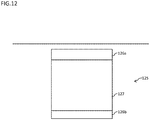
- the capacitor part 125 may include a first capacitor electrode part 126a connected to a first winding-wire-side electrode pad 18a, a second capacitor electrode part 126b connected to a second winding-wire-side electrode pad 18b, and an insulating layer 127 provided between the first capacitor electrode part 126a and the second capacitor electrode part 126b.
- the first winding-wire-side electrode pad 18a may be connected to the resistance part 115 inside the semiconductor layer 1 and connected to the inverting input terminal of the operational amplifier 130 provided outside, and the second winding-wire-side electrode pad 18b may be connected to the output terminal of the operational amplifier 130.
- the capacitor part 125 is schematically shown.
- the other configurations are similar to those of the first embodiment, and any configurations adopted in the first embodiment can be adopted in the second embodiment.
- the members described in the first embodiment will be described with the same reference numerals.
- the first capacitor electrode part 126a and the second capacitor electrode part 126b may be made of polysilicon or the like.
- the capacitor part 125 is not necessarily made of only a semiconductor material, and metal or an insulating material can also be used as appropriate.
- the first capacitor electrode part 126a and the second capacitor electrode part 126b may be made of metal.
- a technique for forming a multilayer ceramic capacitor or a chip capacitor can also be used for forming the capacitor part 125, and a dielectric such as an insulating layer may be sandwiched between a plurality of metal layers or layers made of polysilicon to form a multilayer structure.
- the resistance part 115 and the capacitor part 125 are formed in the semiconductor layer 1. Therefore, an integration circuit can be formed without separately using a resistor and a capacitor, which is advantageous.
- the size can be further reduced, and further, noise generated between the winding wire part 10 and the resistance part 115 and between the resistance part 115 and the capacitor part 125 can be suppressed.
- the present embodiment is also advantageous in that, since the positional relationship between both the resistance part 115 and the capacitor part 125 and the starting end part of the winding wire part 10 is determined in advance, generation of variation in accuracy in detecting a change in current, depending on the positional relationship and the connection mode between both the resistance part 115 and the capacitor part 125 and the winding wire part 10, can be prevented.
- the resistance part 115 and the capacitor part 125 are formed in the semiconductor layer 1.
- the capacitor part 125 is formed in the semiconductor layer 1, but the resistance part 115 is not formed, as shown in Fig. 13 .
- any configurations adopted in the above embodiments can be adopted. The members described in each of the above embodiments will be described with the same reference numerals.
- the starting end part of the winding wire part 10 may be connected to a winding-wire electrode pad 19, and the winding-wire electrode pad 19 may be connected to one end of an externally provided resistor 110.
- the other end of the resistor 110 may be connected to a first capacitor electrode pad 17a and the inverting input terminal of the operational amplifier 130.
- a second capacitor electrode pad 17b may be connected to the output terminal of the operational amplifier 130.
- the first capacitor electrode pad 17a may be connected to the first capacitor electrode part 126a of the capacitor part 125, and the second capacitor electrode pad 17b may be connected to the second capacitor electrode part 126b of the capacitor part 125 (see Fig. 12 ).
- the capacitor part 125 is formed in the semiconductor layer 1. Therefore, an integration circuit can be formed without separately using the capacitor 120, which is advantageous.
- the winding return wire part 50 is provided outside the periphery of the winding wire part 10.
- the winding return wire part 50 is provided inside the periphery of the winding wire part 10 as shown in Fig. 15.
- Fig. 15 corresponds to the first embodiment, and any configurations adopted in the above embodiments can also be adopted in the present embodiment.
- the members described in each of the above embodiments will be described with the same reference numerals.
- the winding wire part 10 may have: a first straight part 11 along a winding direction; a second straight part 12 extending from the end of the first straight part 11 toward the outer peripheral edge (to the left in Fig. 14 ) and extending in the plane direction along the winding direction; a third straight part 13 extending from one side toward the other side from the end of the second straight part 12; a fourth straight part 14 extending from the end of the third straight part 13 toward the inner peripheral edge (to the right in Fig. 14 ) and extending along the direction perpendicular to the winding direction; and a fifth straight part 15 extending toward one side from the other side from the end of the fourth straight part 14 (third aspect) (see Fig. 14 ).
- a sixth straight part 16 extending from the end of the fifth straight part 15 toward the inner peripheral edge (to the right in Fig. 14 ) in the plane direction may be provided at the terminal end part of the winding wire part 10, and the end of the sixth straight part 16 and the starting end part of the winding return wire part 50 may be connected to each other.
- the winding return wire part 50 may extend in the plane direction.
- the winding wire part 10 may have: a first straight part 11 along the winding direction; a second straight part 12 extending from the end of the first straight part 11 toward the outer peripheral edge and extending in the plane direction along the winding direction; a third straight part 13 extending toward one side from the other side from the end of the second straight part 12; a fourth straight part 14 extending from the end of the third straight part 13 toward the inner peripheral edge and extending along the direction perpendicular to the winding direction; and a fifth straight part 15 extending from one side toward the other side from the end of the fourth straight part 14 (fourth aspect).
- a sixth straight part 16 extending from the end of the fifth straight part 15 toward the inner peripheral edge in the plane direction may be provided at the terminal end part of the winding wire part 10, and the end of the sixth straight part 16 and the starting end part of the winding return wire part 50 may be connected to each other.
- the winding return wire part 50 may extend in the plane direction.
- the winding wire part 10 can be positioned outward of the periphery of the winding return wire part 50. Therefore, the length of the winding wire part 10 can be increased, and the number of turns of the winding wire part 10 can be increased. As a result, in some cases, the accuracy in detecting the change in current can be improved, which is advantageous.
- the winding wire part 10 has the A-direction winding wire part 31 extending in the second direction, the B-direction winding wire part 32 connected to the end of the A-direction winding wire part 31 and extending in the third direction, the C-direction winding wire part 33 connected to the end of the B-direction winding wire part 32 and extending in the second direction, and the D-direction winding wire part 34 connected to the end of the C-direction winding wire part 33 and extending in the third direction.
- the present invention is not limited thereto.
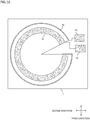
- each of the winding wire part 10 and the winding return wire part 50 may have a circular shape in a plan view (in a plane including the second direction and the third direction) as shown in Fig. 16 .
- each of the winding wire part 10 and the winding return wire part 50 may have a triangular shape in a plan view.
- any configurations adopted in the above embodiments can also be adopted in the present embodiment.
- the members described in each of the above embodiments will be described with the same reference numerals.
- the winding wire part 10 and the winding return wire part 50 are both provided in one semiconductor layer 1.
- the winding wire part 10 is provided in the semiconductor layer 1 provided with the first electrode 61 and the second electrode 62, and the winding return wire part 50 is provided on another semiconductor layer 200 or another member.
- any configurations adopted in the above embodiments can also be adopted in the present embodiment.
- the members described in each of the above embodiments will be described with the same reference numerals.
- the winding return wire part 50 may be made of a metal wire, and may be arranged to surround the periphery of the semiconductor device 100 as shown in Fig. 17(a) .
- a groove 5 may be provided on the side wall of the semiconductor device 100 for positioning the winding return wire part 50.
- the winding return wire part 50 may be formed in a semiconductor layer 200 different from the semiconductor layer 1 provided with the winding wire part 10, and the semiconductor layer 200 may be provided to surround the semiconductor layer 1 provided with the winding wire part 10.
- one quasi Rogowski coil or Rogowski coil is provided.
- a plurality of quasi Rogowski coils or Rogowski coils are provided.
- any configurations adopted in the above embodiments can also be adopted in the present embodiment.
- the members described in each of the above embodiments will be described with the same reference numerals.
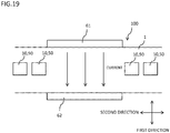
- quasi Rogowski coils or Rogowski coils may be aligned in the first direction. More specifically, the winding wire part 10 and the winding return wire part 50 which does not pass through the winding wire part 10 (a quasi Rogowski coil), or the winding wire part 10 and the winding return wire part 50 passing through the winding wire part 10 (Rogowski coil) may be aligned in the first direction.
- a change in current can be detected at two or more locations in the first direction, which is advantageous in that a change in current can be detected more accurately.
- the manufacturing process becomes complicated as compared with the first embodiment.
- another quasi Rogowski coil or Rogowski coil may be disposed on the outer peripheral side of the quasi Rogowski coil or Rogowski coil. More specifically, the winding wire part 10 and the winding return wire part 50 which does not pass through the winding wire part 10 (quasi Rogowski coil), or the winding wire part 10 and the winding return wire part 50 passing through the winding wire part 10 (Rogowski coil) may be aligned in the second direction or the third direction.
- this aspect is adopted, a change in current can also be detected more accurately, which is advantageous.
- this aspect is also advantageous in that the same manufacturing process as that of the first embodiment can be employed.
- the quasi Rogowski coils or Rogowski coils may be stacked in the first direction, and other quasi Rogowski coils or Rogowski coils may be provided on the outer peripheral side of the quasi Rogowski coils or Rogowski coils. More specifically, the winding wire parts 10 and the winding return wire parts 50 which do not pass through the winding wire parts 10 (quasi Rogowski coils), or the winding wire parts 10 and the winding return wire parts 50 passing through the winding wire parts 10 (Rogowski coils) may be aligned in the second direction or the third direction, and also aligned in the first direction.
- the winding wire part 10, the winding return wire part 50, and the like are provided in the semiconductor device 100.
- the winding wire part 10, the winding return wire part 50, and the like are provided in a semiconductor component 150 different from the semiconductor device 100.
- the other configurations are similar to those of the above embodiments, and any configurations adopted in the above embodiments can be adopted in the present embodiment.
- the semiconductor layer 1 of the semiconductor component 150 is provided with a resistance part 115 or a capacitor part 125, or both of the resistance part 115 and the capacitor part 125.
- the semiconductor component 150 according to the present embodiment may be arranged so as to surround the periphery of the semiconductor device 100 to be measured as shown in Fig. 21 .
- the present embodiment is not limited thereto, and the semiconductor component 150 according to the present embodiment may be provided so as to surround a detection target through which at least a portion of the current flowing in the semiconductor device 100 flows.
- a current flowing through the semiconductor device 100 can be indirectly measured, even if it is difficult to directly measure the current flowing through the semiconductor device 100 due to the positional relationship or the like, and thus, this aspect is advantageous in this point.
- the operational amplifier part 135 may be formed in the semiconductor layer 1 as shown in Fig. 22 (ninth embodiment).
- the resistance part 115, the capacitor part 125, and the operational amplifier part 135 are formed in the semiconductor layer 1, an integration circuit can be formed by these units. Therefore, a change in current can be detected only by the semiconductor device 100, which is advantageous.
- the present invention is not limited thereto.
- the winding return wire part 50 and the winding wire part 10 in the semiconductor layer 1 may be connected to the resistor 110, the capacitor 120, and the operational amplifier 130, which are provided outside of the semiconductor device 100, to form an integration circuit.
Landscapes
- Physics & Mathematics (AREA)
- General Physics & Mathematics (AREA)
- Engineering & Computer Science (AREA)
- Power Engineering (AREA)
- Semiconductor Integrated Circuits (AREA)
- Measuring Instrument Details And Bridges, And Automatic Balancing Devices (AREA)
- Measurement Of Current Or Voltage (AREA)
Abstract
Description
- The present invention relates to a semiconductor device and a semiconductor component having a winding wire part in a semiconductor layer.
- Conventionally, a current detection sensor using a Rogowski coil has been known. The Rogowski coil is a coreless coil, and has a winding core, a winding wire wound around the winding core, and a return wire connected to the terminal end part of the winding wire and returning to a starting end part side (for example, see
JP 2012-88224 A - Meanwhile, a sensor has been proposed which detects a change in current flowing through a semiconductor device (for example, a switching element). However, conventional sensors cannot detect a change in current flowing through the semiconductor device with sufficient accuracy, and there is a problem that the size of the entire device including the sensor may be increased.
- The present invention provides a semiconductor device and a semiconductor component which can be reduced in overall size and which can detect operation with high accuracy.
- A semiconductor device may comprise:
- a first electrode;
- a second electrode; and
- a semiconductor layer having a winding wire part provided so as to surround a current flowing between the first electrode and the second electrode, a winding return wire part which is provided so as to surround the current, is connected to a terminal end part of the winding wire part and returns toward a starting end part side from the terminal end part, and an integration circuit configuration part connected to the winding wire part or the winding return wire part; wherein
- the integration circuit configuration part may have one or more of a resistance part, a capacitor part and an operational amplifier part,
- the resistance part may be electrically connected to the winding wire part or the winding return wire part,
- the capacitor part may be electrically connected to the resistance part or a resistor provided outside, and
- the operational amplifier part may be electrically connected to the resistance part or a resistor provided outside, and the capacitor part or a capacitor provided outside.
- In the semiconductor device according to the present invention,
the integration circuit configuration part may have the resistance part. - In the semiconductor device according to the present invention,
the integration circuit configuration part may have the capacitor part. - In the semiconductor device according to the present invention,
the integration circuit configuration part may have the resistance part and the capacitor part, and
the resistance part and the capacitor part may be electrically connected to an operational amplifier provided outside. - In the semiconductor device according to the present invention,
the integration circuit configuration part may have the resistance part, the capacitor part and the operational amplifier part. - In the semiconductor device according to the present invention,
the winding return wire part may not pass through the winding wire part. - A semiconductor component may comprise a semiconductor layer, wherein
the semiconductor layer may have
a winding wire part provided so as to surround a current;
a winding return wire part which is provided so as to surround the current, is connected to a terminal end part of the winding wire part and returns toward a starting end part side from the terminal end part; and
an integration circuit configuration part connected to the winding wire part or the winding return wire part;
the integration circuit configuration part may have one or more of a resistance part, a capacitor part and an operational amplifier part,
the resistance part may be electrically connected to the winding wire part or the winding return wire part,
the capacitor part may be electrically connected to the resistance part or a resistor provided outside, and
the operational amplifier part may be electrically connected to the resistance part or a resistor provided outside, and the capacitor part or a capacitor provided outside. - Furthermore, according to one aspect of the present invention, at least a part of the integration circuit is formed in the semiconductor layer, so that the entire configuration can be made compact. In addition, at least a part of the integration circuit is disposed closer to the winding wire part, whereby generation of noise can be prevented.
-
-
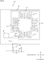
Fig. 1 is a plan view of a semiconductor device that can be used in a first embodiment of the present invention. -
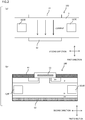
Fig. 2(a) shows a longitudinal cross section of the semiconductor device that can be used in the first embodiment of the present invention, andFig. 2(b) shows a longitudinal cross section of another semiconductor device that can be used in the first embodiment of the present invention. -
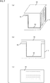
Fig. 3(a) shows a perspective view of the semiconductor device that can be used in the first embodiment of the present invention,Fig. 3(b) is a longitudinal sectional view of the semiconductor device shown inFig. 3(a), and Fig. 3(c) is a plan view of the semiconductor device shown inFig. 3(a). Fig. 3(a) does not illustrate the right part of the device shown inFigs. 3(b) and 3(c) in order to show a longitudinal cross section different from that shown inFig. 3(b) . -
Fig. 4(a) shows a perspective view for describing a manufacturing step of the semiconductor device that can be used in the first embodiment of the present invention,Fig. 4(b) is a longitudinal sectional view of the semiconductor device shown inFig. 4(a), and Fig. 4(c) is a plan view of the semiconductor device shown inFig. 4(a). Fig. 4(a) does not illustrate the right part of the device shown inFigs. 4(b) and 4(c) in order to show a longitudinal cross section different from that shown inFig. 4(b) . -
Fig. 5(a) shows a perspective view for describing a manufacturing step subsequent to the step inFig. 4(a) ,Fig. 5(b) is a longitudinal sectional view of the semiconductor device shown inFig. 5(a), and Fig. 5(c) is a plan view of the semiconductor device shown inFig. 5(a) . -
Fig. 6(a) shows a perspective view for describing a manufacturing step subsequent to the step inFig. 5(a) ,Fig. 6(b) is a longitudinal sectional view of the semiconductor device shown inFig. 6(a), and Fig. 6(c) is a plan view of the semiconductor device shown inFig. 6(a) . -
Fig. 7(a) shows a perspective view for describing a manufacturing step subsequent to the step inFig. 6(a) ,Fig. 7(b) is a longitudinal sectional view of the semiconductor device shown inFig. 7(a), and Fig. 7(c) is a plan view of the semiconductor device shown inFig. 7(a) . -
Fig. 8(a) shows a perspective view for describing a manufacturing step subsequent to the step inFig. 7(a) ,Fig. 8(b) is a longitudinal sectional view of the semiconductor device shown inFig. 8(a), and Fig. 8(c) is a plan view of the semiconductor device shown inFig. 8(a) . -
Fig. 9 is a longitudinal sectional view of still another semiconductor device that can be used in the first embodiment of the present invention. In order to show that a winding return wire part passes through a winding wire part,Fig. 9 also shows a second straight part on the front surface side of the page which is invisible in the longitudinal cross section. -
Fig. 10 is a longitudinal sectional view of a resistance part that can be used in the first embodiment of the present invention. -
Fig. 11 is a plan view of a semiconductor device that can be used in a second embodiment of the present invention. -
Fig. 12 is a longitudinal sectional view of a capacitor part that can be used in the second embodiment of the present invention. -
Fig. 13 is a plan view of a semiconductor device that can be used in a third embodiment of the present invention. -
Fig. 14 is a longitudinal sectional view of a semiconductor device that can be used in a fourth embodiment of the present invention. -
Fig. 15 is a plan view of the semiconductor device that can be used in the fourth embodiment of the present invention. -
Fig. 16 is a plan view of a semiconductor device that can be used in a fifth embodiment of the present invention. -
Fig. 17(a) shows a longitudinal cross section of a semiconductor device that can be used in a sixth embodiment of the present invention, andFig. 17(b) shows a longitudinal cross section of another semiconductor device that can be used in the sixth embodiment of the present invention. -
Fig. 18 shows a longitudinal cross section of a semiconductor device that can be used in a seventh embodiment of the present invention. -
Fig. 19 shows a longitudinal cross section of a semiconductor device that can be used in another aspect of the seventh embodiment of the present invention. -
Fig. 20 shows a longitudinal cross section of a semiconductor device that can be used in still another aspect of the seventh embodiment of the present invention. -
Fig. 21(a) shows longitudinal cross sections of a semiconductor component and a semiconductor device that can be used in an eighth embodiment of the present invention, andFig. 21(b) shows longitudinal cross sections of a semiconductor component and a semiconductor device that can be used in another aspect of the eighth embodiment of the present invention. -
Fig. 22 is a plan view of a semiconductor device that can be used in a ninth embodiment of the present invention. -
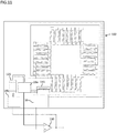
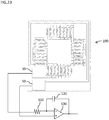
Fig. 23 is a plan view of a semiconductor device that can be used in the present invention. - In the present embodiment, "one side" means the upper side in
Fig. 2 and "other side" means the lower side inFig. 2 . Further, the vertical direction inFig. 2 (the direction toward one side from the other side and the direction from one side toward the other side) is referred to as a "first direction", the horizontal direction inFig. 2 is referred to as a "second direction", and the front-back direction of the page ofFig. 2 is referred to as a "third direction". An in-plane direction including the second direction and the third direction is referred to as a "plane direction", and a state where the device is viewed from the upper side inFig. 2 is referred to as a "plan view". - As shown in
Fig. 2(a) , asemiconductor device 100 according to the present embodiment may have afirst electrode 61; asecond electrode 62; and a semiconductor layer 1 (see alsoFig. 1 ) including a windingwire part 10 provided so as to surround a current flowing between thefirst electrode 61 and thesecond electrode 62, and a windingreturn wire part 50, which is provided so as to surround the current, is connected to the terminal end part of the windingwire part 10 and returns toward the starting end part side from the terminal end part. Examples of usable materials for the semiconductor include silicon, silicon carbide, and gallium nitride.Fig. 2(a) shows an aspect in which the current flows from the upper side toward the lower side. However, this is merely an example, and the current may flow from the lower side toward the upper side. - The winding
wire part 10 and the windingreturn wire part 50 may be formed of a semiconductor material such as polysilicon, but not limited thereto. They may be formed of a metal material such as copper and aluminum, and the metal film may serve as the windingwire part 10 and the windingreturn wire part 50. - The winding
return wire part 50 may be configured not to pass through the windingwire part 10. In the present embodiment, the windingreturn wire part 50 is provided to surround the outer periphery of the windingwire part 10 as shown inFig. 1 . The inside of the windingwire part 10 may be filled with an insulating material such as an oxide film (see a later-described thirdinsulating film 93 shown inFig. 3 ). - Although
Fig. 1 shows the aspect in which the windingreturn wire part 50 does not pass through the windingwire part 10, the present invention is not limited thereto, and the windingreturn wire part 50 may pass through the windingwire part 10 as shown inFig. 9 . In the present embodiment, the aspect shown inFig. 1 is referred to as a "quasi Rogowski coil", and the aspect shown inFig. 9 is referred to as a "Rogowski coil". Use of reference numerals "10, 50" inFig. 2 indicates that the quasi Rogowski coil may be used or the Rogowski coil may be used. - As shown in
Fig. 3 , the windingwire part 10 may have: a firststraight part 11 along a winding direction; a secondstraight part 12 extending toward the inner peripheral edge (to the right inFig. 3 ) from the end of the firststraight part 11 and extending in a plane direction (direction including the second direction and the third direction) along the winding direction; a thirdstraight part 13 extending from one side toward the other side from the end of the secondstraight part 12; a fourthstraight part 14 extending toward the outer peripheral edge (to the left side inFig. 3 ) from the end of the thirdstraight part 13 and extending in the plane direction along the direction perpendicular to the winding direction; and a fifthstraight part 15 extending toward one side from the other side from the end of the fourth straight part 14 (first aspect). Further, a sixthstraight part 16 extending toward the outer peripheral edge from the end of the fifthstraight part 15 in the plane direction may be provided at the terminal end part of the windingwire part 10, and the end of the sixthstraight part 16 and the starting end part of the windingreturn wire part 50 may be connected to each other. The windingreturn wire part 50 may extend in the plane direction. - Unlike the aspect described above, the winding
wire part 10 may have: a firststraight part 11 along a winding direction; a secondstraight part 12 extending toward the inner peripheral edge from the end of the firststraight part 11 and extending in a plane direction along the winding direction; a thirdstraight part 13 extending toward one side from the other side from the end of the secondstraight part 12; a fourthstraight part 14 extending toward the outer peripheral edge from the end of the thirdstraight part 13 and extending in the plane direction along the direction perpendicular to the winding direction; and a fifthstraight part 15 extending from one side toward the other side from the end of the fourth straight part 14 (second aspect). Further, a sixthstraight part 16 extending toward the outer peripheral edge from the end of the fifthstraight part 15 in the plane direction may be provided at the terminal end part of the windingwire part 10, and the end of the sixthstraight part 16 and the starting end part of the windingreturn wire part 50 may be connected to each other. The windingreturn wire part 50 may extend in the plane direction. - Considering that the manufacturing method to be described later is adopted, it is advantageous to use the first aspect described first instead of the second aspect described later, because the winding
return wire part 50 can be positioned on one side, which leads to simplified manufacturing process. - The
first electrode 61 may be provided on a first main surface, and thesecond electrode 62 may be provided on a second main surface. InFig. 2 , the upper surface is defined as the first main surface, and the lower surface is defined as the second main surface. Thesemiconductor device 100 may be a switching element, and may be, for example, a vertical MOSFET. When the aspect of the present embodiment is adopted for the vertical MOSFET, thefirst electrode 61 may be a source electrode and thesecond electrode 62 may be a drain electrode as shown inFig. 2(b) . A quasi Rogowski coil may be provided so as to surround the current flowing between the source electrode and the drain electrode. Note thatreference numeral 63 inFig. 2(b) denotes a gate electrode. - As shown in
Fig. 1 , aresistance part 115 may be provided in thesemiconductor layer 1 in the present embodiment. The starting end part of the windingwire part 10 may be connected to theresistance part 115 formed in thesemiconductor layer 1, and theresistance part 115 may be connected to a winding-wire-side electrode pad 18. The winding-wire-side electrode pad 18 may be connected to one end of acapacitor 120 provided outside and the inverting input terminal of anoperational amplifier 130, and a return-wire electrode pad 59 connected to the terminal end part of the windingreturn wire part 50 may be connected to the non-inverting input terminal of theoperational amplifier 130. The other end of thecapacitor 120 may be connected to the output terminal of theoperational amplifier 130. InFig. 1 , theresistance part 115 to be described later is schematically shown. - As shown in
Fig. 10 , theresistance part 115 may include a firstresistance electrode part 118a connected to the windingwire part 10, a secondresistance electrode part 118b connected to the winding-wire-side electrode pad 18, aresistance element 117 provided between the firstresistance electrode part 118a and the secondresistance electrode part 118b, and insulatinglayers resistance element 117. The firstresistance electrode part 118a and the secondresistance electrode part 118b may be made of polysilicon or the like. Theresistance part 115 is not necessarily made of only a semiconductor material, and metal or an insulating material can also be used as appropriate. For example, the firstresistance electrode part 118a and the secondresistance electrode part 118b may be made of metal. Theresistance element 117 may be made of, for example, ruthenium oxide or Ag/Pd. Note that, for example, a technique for producing aresistor 110 can be used for forming theresistance part 115. Further, the resistance of theresistance part 115 may be varied by adjusting the impurity concentration in thesemiconductor layer 1. - As shown in
Fig. 1 , the windingwire part 10 may have an A-direction windingwire part 31 extending in the second direction, a B-direction windingwire part 32 connected to the end of the A-direction windingwire part 31 and extending in the third direction, a C-direction windingwire part 33 connected to the end of the B-direction windingwire part 32 and extending in the second direction, and a D-direction windingwire part 34 connected to the end of the C-direction windingwire part 33 and extending in the third direction. When the aspect described above is employed, the A- to D- direction windingwire parts 31 to 34 can be linearly formed, which is advantageous in that they can be manufactured relatively easily. The present embodiment describes the aspect using four direction windingwire parts 31 to 34. However, the present invention is not limited thereto, and three direction winding wire parts may be used to form a triangular shape in the plane direction, or five or more direction winding wire parts may be used to form a polygonal shape in the plane direction. - The A-direction winding
wire part 31, the B-direction windingwire part 32, the C-direction windingwire part 33, and the D-direction windingwire part 34 may correspond to each other in length. The state where they correspond to each other in length indicates that the length of the A-direction windingwire part 31, the length of the B-direction windingwire part 32, the length of the C-direction windingwire part 33, and the length of the D-direction windingwire part 34 are respectively within the range of ±5% of the average value of the A-direction windingwire part 31, the B-direction windingwire part 32, the C-direction windingwire part 33, and the D-direction windingwire part 34. The numbers of turns included in the A-direction windingwire part 31, the B-direction windingwire part 32, the C-direction windingwire part 33, and the D-direction windingwire part 34 may be the same. The number of turns of the A-direction windingwire part 31 may be less than the numbers of turns of the B-direction windingwire part 32, the C-direction windingwire part 33, and the D-direction windingwire part 34 by, for example, one, two, or more. - In the above aspect, the linear part is described using a "straight part". That is, the aspect is described using the first
straight part 11 as an example of the first linear part, the secondstraight part 12 as an example of the second linear part, the thirdstraight part 13 as an example of the third linear part, the fourthstraight part 14 as an example of the fourth linear part, the fifthstraight part 15 as an example of the fifth linear part, and the sixthstraight part 16 as an example of the sixth linear part. However, the present invention is not limited thereto. The respective linear parts may be curved, or only some of the plurality of linear parts may be straight parts. In view of facilitating the manufacturing process, it is advantageous that the second linear part and the fourth linear part are straight parts, that is, the secondstraight part 12 and the fourthstraight part 14, respectively. - Further, in the above aspect, the longitudinal cross section has a rectangular shape by the second
straight part 12, the thirdstraight part 13, the fourthstraight part 14, and the fifth straight part 15 (seeFigs. 3 and9 ). However, the present invention is not limited thereto, and the longitudinal cross section may have a triangular shape or a polygonal shape (polygon having five or more corners) having more corners. - Next, an example of a method for manufacturing the
semiconductor device 100 according to the present embodiment will be described. - A first insulating
film 91 made of an oxide film or the like is formed on the upper surface of thesemiconductor layer 1 such as a wafer with a thermal oxide film or chemical vapor deposition (CVD) (seeFig. 4 ). Note that the first insulatingfilm 91 also includes a resist film. - Next, a region for forming a trench is patterned by photolithography, and thereafter, the first insulating
film 91 is dry etched (seeFig. 4 ). - Then, the
semiconductor layer 1 is dry etched using the first insulatingfilm 91 as a mask (seeFig. 5 ). The damaged layer on the etched side wall may be removed by chemical dry etching (CDE), sacrificial oxide film, H2 annealing, or the like. - Next, a second insulating
film 92 such as a thermal oxide film or a CVD oxide film is formed on the inner sidewall and the inner bottom surface of the trench (seeFig. 6 ). When the first insulatingfilm 91 is composed of, for example, a resist film, the first insulatingfilm 91 may be removed before the second insulatingfilm 92 is formed, and then the second insulatingfilm 92 may be formed, unlike the above aspect. - Then, the inside of the trench is filled with a
conductive material 95 such as polysilicon, and theconductive material 95 such as polysilicon is also stacked on the upper surface of the first insulating film 91 (seeFig. 7 ). With this process, theconductive material 95 is provided inside the trench in which the second insulatingfilm 92 is formed and on the first insulatingfilm 91. In this case, the thickness of theconductive material 95 stacked on the first insulatingfilm 91 may be, for example, about 0.5 µm to 2 µm. - Next, patterning for forming the winding
wire part 10 and the windingreturn wire part 50 is performed by photolithography (seeFig. 8 ). In this process, the thickness of theconductive material 95 remaining on the inner bottom surface and the inner side surface of the trench may be the same as the thickness of theconductive material 95 stacked on the first insulatingfilm 91, and may be, for example, about 0.5 µm to 2 µm. Due to forming theconductive materials 95 to have the same thickness as described above, the current flowing through the respectivestraight parts 11 to 16 and the windingreturn wire part 50 can be made constant, which is advantageous in that the detection accuracy can be enhanced. - Next, the inside of the trench is embedded with an insulating material such as an oxide film, and the insulating material is also stacked on the upper surface (see
Fig. 3 ). More specifically, the third insulatingfilm 93 such as an oxide film is embedded by CVD or spin on glass (SOG), and the third insulatingfilm 93 such as an interlayer insulating film is provided on the upper surface. - Next, photolithography is performed to open a contact hole in the third insulating
film 93 such as an interlayer insulating film at the starting end part of the windingwire part 10 and the terminal end part of the windingreturn wire part 50 formed of theconductive material 95 such as polysilicon. Thereafter, a contact hole is opened in the third insulatingfilm 93 such as an interlayer insulating film by dry etching, and metal to be a PAD for an electrode wire or the like is formed at the portion where the contact hole is opened, so as to form the winding-wire-side electrode pad 18 and the return-wire electrode pad 59 (seeFig. 1 ). - Subsequently, an example of the operation and effect according to the present embodiment configured as described above will be described. All the aspects to be described in "operation and effect" can be employed in the above configuration.
- When the winding
wire part 10 as in the present embodiment is adopted, the configuration of the windingwire part 10 can be miniaturized by utilizing the technique for manufacturing thesemiconductor device 100, and the number of turns per unit length can be increased. Therefore, a change in current (the operation of the semiconductor device 100) can be detected accurately. Further, since miniaturization is enabled as described above, an increase in size of thesemiconductor device 100 can be prevented, even if the windingwire part 10 and the windingreturn wire part 50 are provided in thesemiconductor layer 1. - Further, the winding
wire part 10 and the windingreturn wire part 50 are formed in thesemiconductor layer 1 of thesemiconductor device 100 in which the arrangement positions of thefirst electrode 61 and thesecond electrode 62 are determined as in the present embodiment, whereby the windingwire part 10 and the windingreturn wire part 50 can be positioned with respect to the current which is to be measured and which is flowing between thefirst electrode 61 and thesecond electrode 62. In addition, since no positional deviation occurs, there is no influence by the positional deviation. For this reason, it is possible to measure the change in current without variation. - The application of the aspect in which the winding
return wire part 50 does not pass through the windingwire part 10 is significantly advantageous in that the manufacturing process can be facilitated. Specifically, when the aspect shown inFig. 9 in which the windingreturn wire part 50 passes through the windingwire part 10 is employed, the process for forming the windingreturn wire part 50 inside the windingwire part 10 becomes complicated, which leads to an increase in manufacturing cost. On the other hand, when the windingreturn wire part 50 is not formed inside the windingwire part 10 as described with reference toFigs. 3 to 8 , the manufacturing process can be remarkably facilitated, and the manufacturing cost can be reduced. Thus, this aspect is advantageous. - In a case where the
semiconductor device 100 is a switching element such as a MOSFET, a current changes when thedevice 100 is switched between ON and OFF. In view of this, the use of the quasi Rogowski coil and the Rogowski coil according to the present embodiment is advantageous. - As shown in
Fig. 2 , when the aspect in which thefirst electrode 61 is provided on the first main surface of thesemiconductor layer 1 and thesecond electrode 62 is provided on the second main surface of thesemiconductor layer 1 is used, a current flows between the first main surface and the second main surface, and the windingwire part 10 and the windingreturn wire part 50 are provided so as to surround the current. Therefore, the manufacturing method as described above (seeFigs. 3 to 8 ) can be used. Thus, the manufacturing process can be simplified, which is advantageous in that a practical manufacturing method can be established in consideration of mass production. - When the aspect in which the first
straight part 11, the secondstraight part 12, and the sixthstraight part 16 of the windingwire part 10 and the windingreturn wire part 50 are the same in height as shown inFigs. 3(a) and 3(b) , the same process can be used for these parts as shown inFigs. 7 and8 , which is advantageous. That is, this aspect is advantageous in that these parts can be formed by stacking theconductive material 95 on the upper surface of the first insulating film 91 (seeFig. 7 ) and etching the conductive material 95 (seeFig. 8 ). - When the present embodiment is used, the winding
return wire part 50 can be positioned outward of the periphery of the windingwire part 10. For this reason, the present embodiment is advantageous in that the windingwire part 10 can be disposed as close to the current flowing between thefirst electrode 61 and thesecond electrode 62 as possible. - In the present embodiment, the
resistance part 115 connected to thecapacitor 120 and theoperational amplifier 130 is formed in thesemiconductor layer 1 as shown inFig. 1 . Therefore, an integration circuit can be formed without separately using a resistor, and the like, which is advantageous. An aspect where theoperational amplifier 130 is not used as the integration circuit is also considered, and in such a case, it is only necessary that thesemiconductor device 100 of the present embodiment is connected to thecapacitor 120. - In addition, due to the
resistance part 115 being incorporated in thesemiconductor layer 1, the size can be further reduced, and further, noise generated between the windingwire part 10 and theresistance part 115 can be suppressed. - In addition, the present embodiment is also advantageous in that, since the positional relationship between the
resistance part 115 and the starting end part of the windingwire part 10 is determined in advance, generation of variation in accuracy in detecting a change in current, depending on the positional relationship and the connection mode between theresistance part 115 and the windingwire part 10, can be prevented. - Next, a second embodiment of the present invention will be described.
- In the first embodiment, the
resistance part 115 is formed in thesemiconductor layer 1. In contrast, in the present embodiment, acapacitor part 125 is formed in thesemiconductor layer 1 in addition to theresistance part 115 as shown inFig. 11 . As shown inFig. 12 , thecapacitor part 125 may include a firstcapacitor electrode part 126a connected to a first winding-wire-side electrode pad 18a, a secondcapacitor electrode part 126b connected to a second winding-wire-side electrode pad 18b, and an insulatinglayer 127 provided between the firstcapacitor electrode part 126a and the secondcapacitor electrode part 126b. As shown inFig. 11 , the first winding-wire-side electrode pad 18a may be connected to theresistance part 115 inside thesemiconductor layer 1 and connected to the inverting input terminal of theoperational amplifier 130 provided outside, and the second winding-wire-side electrode pad 18b may be connected to the output terminal of theoperational amplifier 130. InFig. 11 , thecapacitor part 125 is schematically shown. The other configurations are similar to those of the first embodiment, and any configurations adopted in the first embodiment can be adopted in the second embodiment. The members described in the first embodiment will be described with the same reference numerals. - The first
capacitor electrode part 126a and the secondcapacitor electrode part 126b may be made of polysilicon or the like. Thecapacitor part 125 is not necessarily made of only a semiconductor material, and metal or an insulating material can also be used as appropriate. For example, the firstcapacitor electrode part 126a and the secondcapacitor electrode part 126b may be made of metal. A technique for forming a multilayer ceramic capacitor or a chip capacitor can also be used for forming thecapacitor part 125, and a dielectric such as an insulating layer may be sandwiched between a plurality of metal layers or layers made of polysilicon to form a multilayer structure. - In the present embodiment, the
resistance part 115 and thecapacitor part 125 are formed in thesemiconductor layer 1. Therefore, an integration circuit can be formed without separately using a resistor and a capacitor, which is advantageous. - In addition, due to the
resistance part 115 and thecapacitor part 125 being incorporated in thesemiconductor layer 1, the size can be further reduced, and further, noise generated between the windingwire part 10 and theresistance part 115 and between theresistance part 115 and thecapacitor part 125 can be suppressed. - In addition, the present embodiment is also advantageous in that, since the positional relationship between both the
resistance part 115 and thecapacitor part 125 and the starting end part of the windingwire part 10 is determined in advance, generation of variation in accuracy in detecting a change in current, depending on the positional relationship and the connection mode between both theresistance part 115 and thecapacitor part 125 and the windingwire part 10, can be prevented. - Next, a third embodiment of the present invention will be described.
- In the second embodiment, the
resistance part 115 and thecapacitor part 125 are formed in thesemiconductor layer 1. In contrast, in the present embodiment, thecapacitor part 125 is formed in thesemiconductor layer 1, but theresistance part 115 is not formed, as shown inFig. 13 . For the other configurations, any configurations adopted in the above embodiments can be adopted. The members described in each of the above embodiments will be described with the same reference numerals. - The starting end part of the winding
wire part 10 may be connected to a winding-wire electrode pad 19, and the winding-wire electrode pad 19 may be connected to one end of an externally providedresistor 110. The other end of theresistor 110 may be connected to a firstcapacitor electrode pad 17a and the inverting input terminal of theoperational amplifier 130. A secondcapacitor electrode pad 17b may be connected to the output terminal of theoperational amplifier 130. The firstcapacitor electrode pad 17a may be connected to the firstcapacitor electrode part 126a of thecapacitor part 125, and the secondcapacitor electrode pad 17b may be connected to the secondcapacitor electrode part 126b of the capacitor part 125 (seeFig. 12 ). - In the present embodiment, the
capacitor part 125 is formed in thesemiconductor layer 1. Therefore, an integration circuit can be formed without separately using thecapacitor 120, which is advantageous. - Next, a fourth embodiment of the present invention will be described.
- In the above embodiments, the winding
return wire part 50 is provided outside the periphery of the windingwire part 10. In contrast, in the present embodiment, the windingreturn wire part 50 is provided inside the periphery of the windingwire part 10 as shown inFig. 15. Fig. 15 corresponds to the first embodiment, and any configurations adopted in the above embodiments can also be adopted in the present embodiment. The members described in each of the above embodiments will be described with the same reference numerals. - In the present embodiment, unlike the first embodiment, the winding
wire part 10 may have: a firststraight part 11 along a winding direction; a secondstraight part 12 extending from the end of the firststraight part 11 toward the outer peripheral edge (to the left inFig. 14 ) and extending in the plane direction along the winding direction; a thirdstraight part 13 extending from one side toward the other side from the end of the secondstraight part 12; a fourthstraight part 14 extending from the end of the thirdstraight part 13 toward the inner peripheral edge (to the right inFig. 14 ) and extending along the direction perpendicular to the winding direction; and a fifthstraight part 15 extending toward one side from the other side from the end of the fourth straight part 14 (third aspect) (seeFig. 14 ). Further, a sixthstraight part 16 extending from the end of the fifthstraight part 15 toward the inner peripheral edge (to the right inFig. 14 ) in the plane direction may be provided at the terminal end part of the windingwire part 10, and the end of the sixthstraight part 16 and the starting end part of the windingreturn wire part 50 may be connected to each other. The windingreturn wire part 50 may extend in the plane direction. - Alternatively, unlike the aspect described above, the winding
wire part 10 may have: a firststraight part 11 along the winding direction; a secondstraight part 12 extending from the end of the firststraight part 11 toward the outer peripheral edge and extending in the plane direction along the winding direction; a thirdstraight part 13 extending toward one side from the other side from the end of the secondstraight part 12; a fourthstraight part 14 extending from the end of the thirdstraight part 13 toward the inner peripheral edge and extending along the direction perpendicular to the winding direction; and a fifthstraight part 15 extending from one side toward the other side from the end of the fourth straight part 14 (fourth aspect). Further, a sixthstraight part 16 extending from the end of the fifthstraight part 15 toward the inner peripheral edge in the plane direction may be provided at the terminal end part of the windingwire part 10, and the end of the sixthstraight part 16 and the starting end part of the windingreturn wire part 50 may be connected to each other. The windingreturn wire part 50 may extend in the plane direction. - Considering that the manufacturing method used in the first embodiment is adopted, it is advantageous to use the third aspect described first instead of the fourth aspect described later, because the winding
return wire part 50 can be positioned on one side, which leads to a simplified manufacturing process. - When the present embodiment is used, the winding
wire part 10 can be positioned outward of the periphery of the windingreturn wire part 50. Therefore, the length of the windingwire part 10 can be increased, and the number of turns of the windingwire part 10 can be increased. As a result, in some cases, the accuracy in detecting the change in current can be improved, which is advantageous. - Next, a fifth embodiment of the present invention will be described.
- The above embodiments have described the aspect in which the winding
wire part 10 has the A-direction windingwire part 31 extending in the second direction, the B-direction windingwire part 32 connected to the end of the A-direction windingwire part 31 and extending in the third direction, the C-direction windingwire part 33 connected to the end of the B-direction windingwire part 32 and extending in the second direction, and the D-direction windingwire part 34 connected to the end of the C-direction windingwire part 33 and extending in the third direction. However, the present invention is not limited thereto. As an example, each of the windingwire part 10 and the windingreturn wire part 50 may have a circular shape in a plan view (in a plane including the second direction and the third direction) as shown inFig. 16 . Alternatively, each of the windingwire part 10 and the windingreturn wire part 50 may have a triangular shape in a plan view. For the other configurations, any configurations adopted in the above embodiments can also be adopted in the present embodiment. The members described in each of the above embodiments will be described with the same reference numerals. - When the aspect shown in
Fig. 16 is adopted, balanced detection of the current flowing between thefirst electrode 61 and thesecond electrode 62 can be expected. In view of facilitating the manufacturing process, it is advantageous to use an aspect in which straight shaped parts such as the A-direction windingwire part 31, the B-direction windingwire part 32, the C-direction windingwire part 33, and the D-direction windingwire part 34 as in the first and second embodiments are joined to each other. - Next, a sixth embodiment of the present invention will be described.
- In the above embodiments, the winding
wire part 10 and the windingreturn wire part 50 are both provided in onesemiconductor layer 1. In contrast, in the present embodiment, only the windingwire part 10 is provided in thesemiconductor layer 1 provided with thefirst electrode 61 and thesecond electrode 62, and the windingreturn wire part 50 is provided on anothersemiconductor layer 200 or another member. For the other configurations, any configurations adopted in the above embodiments can also be adopted in the present embodiment. The members described in each of the above embodiments will be described with the same reference numerals. - As an example, the winding
return wire part 50 may be made of a metal wire, and may be arranged to surround the periphery of thesemiconductor device 100 as shown inFig. 17(a) . In this case, agroove 5 may be provided on the side wall of thesemiconductor device 100 for positioning the windingreturn wire part 50. - Alternatively, as shown in
Fig. 17(b) , the windingreturn wire part 50 may be formed in asemiconductor layer 200 different from thesemiconductor layer 1 provided with the windingwire part 10, and thesemiconductor layer 200 may be provided to surround thesemiconductor layer 1 provided with the windingwire part 10. - Next, a seventh embodiment of the present invention will be described.
- In the above embodiments, one quasi Rogowski coil or Rogowski coil is provided. In contrast, in the present embodiment, a plurality of quasi Rogowski coils or Rogowski coils are provided. For the other configurations, any configurations adopted in the above embodiments can also be adopted in the present embodiment. The members described in each of the above embodiments will be described with the same reference numerals.
- As shown in
Fig. 18 , quasi Rogowski coils or Rogowski coils may be aligned in the first direction. More specifically, the windingwire part 10 and the windingreturn wire part 50 which does not pass through the winding wire part 10 (a quasi Rogowski coil), or the windingwire part 10 and the windingreturn wire part 50 passing through the winding wire part 10 (Rogowski coil) may be aligned in the first direction. When this aspect is adopted, a change in current can be detected at two or more locations in the first direction, which is advantageous in that a change in current can be detected more accurately. However, in this aspect, it should be noted that, since the windingwire part 10 and the windingreturn wire part 50 need to be arranged so as to be stacked in the first direction, the manufacturing process becomes complicated as compared with the first embodiment. - As shown in
Fig. 19 , another quasi Rogowski coil or Rogowski coil may be disposed on the outer peripheral side of the quasi Rogowski coil or Rogowski coil. More specifically, the windingwire part 10 and the windingreturn wire part 50 which does not pass through the winding wire part 10 (quasi Rogowski coil), or the windingwire part 10 and the windingreturn wire part 50 passing through the winding wire part 10 (Rogowski coil) may be aligned in the second direction or the third direction. When this aspect is adopted, a change in current can also be detected more accurately, which is advantageous. In addition, this aspect is also advantageous in that the same manufacturing process as that of the first embodiment can be employed. - These aspects may be combined, and as shown in
Fig. 20 , the quasi Rogowski coils or Rogowski coils may be stacked in the first direction, and other quasi Rogowski coils or Rogowski coils may be provided on the outer peripheral side of the quasi Rogowski coils or Rogowski coils. More specifically, the windingwire parts 10 and the windingreturn wire parts 50 which do not pass through the winding wire parts 10 (quasi Rogowski coils), or the windingwire parts 10 and the windingreturn wire parts 50 passing through the winding wire parts 10 (Rogowski coils) may be aligned in the second direction or the third direction, and also aligned in the first direction. - Next, an eighth embodiment of the present invention will be described.
- In the above embodiments, the winding
wire part 10, the windingreturn wire part 50, and the like are provided in thesemiconductor device 100. In contrast, in the present embodiment, the windingwire part 10, the windingreturn wire part 50, and the like are provided in asemiconductor component 150 different from thesemiconductor device 100. The other configurations are similar to those of the above embodiments, and any configurations adopted in the above embodiments can be adopted in the present embodiment. In the aspect of the present embodiment, thesemiconductor layer 1 of thesemiconductor component 150 is provided with aresistance part 115 or acapacitor part 125, or both of theresistance part 115 and thecapacitor part 125. - When the
semiconductor component 150 as in the present embodiment is used, a change in current can be measured for an existingsemiconductor device 100 as well, which is advantageous. - For example, the
semiconductor component 150 according to the present embodiment may be arranged so as to surround the periphery of thesemiconductor device 100 to be measured as shown inFig. 21 . The present embodiment is not limited thereto, and thesemiconductor component 150 according to the present embodiment may be provided so as to surround a detection target through which at least a portion of the current flowing in thesemiconductor device 100 flows. When the aspect described above is employed, a current flowing through thesemiconductor device 100 can be indirectly measured, even if it is difficult to directly measure the current flowing through thesemiconductor device 100 due to the positional relationship or the like, and thus, this aspect is advantageous in this point. - Although the above embodiments have been described using the aspect in which the
operational amplifier 130 is provided outside, the present invention is not limited thereto, and theoperational amplifier part 135 may be formed in thesemiconductor layer 1 as shown inFig. 22 (ninth embodiment). In the case where theresistance part 115, thecapacitor part 125, and theoperational amplifier part 135 are formed in thesemiconductor layer 1, an integration circuit can be formed by these units. Therefore, a change in current can be detected only by thesemiconductor device 100, which is advantageous. - The foregoing descriptions of the embodiments and the disclosure of the drawings are merely one example for describing the present invention recited in the claims. The present invention recited in the claims shall not be limited by the foregoing descriptions of the embodiments and the disclosure of the drawings. Further, the recitations of the claims at the time of the filing of the present application are merely an example, and the recitations of the claims can be changed as appropriate based on the description of the specification, the drawings, and the like.
- The above embodiments have been described using the aspect in which at least one of the
resistance part 115 and thecapacitor part 125 is formed in thesemiconductor layer 1. However, the present invention is not limited thereto. As shown inFig. 23 , the windingreturn wire part 50 and the windingwire part 10 in thesemiconductor layer 1 may be connected to theresistor 110, thecapacitor 120, and theoperational amplifier 130, which are provided outside of thesemiconductor device 100, to form an integration circuit. -
- 1
- semiconductor layer
- 10
- winding wire part
- 50
- winding return wire part
- 61
- first electrode
- 62
- second electrode
- 100
- semiconductor device
- 150
- semiconductor component
- 110
- resistor
- 115
- resistance part
- 120
- capacitor
- 125
- capacitor part
- 130
- operational amplifier
- 135
- operational amplifier part
Claims (7)
- A semiconductor device comprising:a first electrode;a second electrode; anda semiconductor layer having a winding wire part provided so as to surround a current flowing between the first electrode and the second electrode, a winding return wire part which is provided so as to surround the current, is connected to a terminal end part of the winding wire part and returns toward a starting end part side from the terminal end part, and an integration circuit configuration part connected to the winding wire part or the winding return wire part; whereinthe integration circuit configuration part has one or more of a resistance part, a capacitor part and an operational amplifier part,the resistance part is electrically connected to the winding wire part or the winding return wire part,the capacitor part is electrically connected to the resistance part or a resistor provided outside, andthe operational amplifier part is electrically connected to the resistance part or a resistor provided outside, and the capacitor part or a capacitor provided outside.
- The semiconductor device according to claim 1, wherein
the integration circuit configuration part has the resistance part. - The semiconductor device according to claim 1 or 2, wherein
the integration circuit configuration part has the capacitor part. - The semiconductor device according to any one of claims 1 to 3, wherein
the integration circuit configuration part has the resistance part and the capacitor part, and
the resistance part and the capacitor part are electrically connected to an operational amplifier provided outside. - The semiconductor device according to any one of claims 1 to 3, wherein
the integration circuit configuration part has the resistance part, the capacitor part and the operational amplifier part. - The semiconductor device according to any one of claims 1 to 5, wherein
the winding return wire part does not pass through the winding wire part. - A semiconductor component comprising a semiconductor layer, wherein
the semiconductor layer has
a winding wire part provided so as to surround a current;
a winding return wire part which is provided so as to surround the current, is connected to a terminal end part of the winding wire part and returns toward a starting end part side from the terminal end part; and
an integration circuit configuration part connected to the winding wire part or the winding return wire part;
the integration circuit configuration part has one or more of a resistance part, a capacitor part and an operational amplifier part,
the resistance part is electrically connected to the winding wire part or the winding return wire part,
the capacitor part is electrically connected to the resistance part or a resistor provided outside, and
the operational amplifier part is electrically connected to the resistance part or a resistor provided outside, and the capacitor part or a capacitor provided outside.
Applications Claiming Priority (1)
| Application Number | Priority Date | Filing Date | Title |
|---|---|---|---|
| PCT/JP2017/042133 WO2019102572A1 (en) | 2017-11-24 | 2017-11-24 | Semiconductor device and semiconductor component |
Publications (2)
| Publication Number | Publication Date |
|---|---|
| EP3715870A1 true EP3715870A1 (en) | 2020-09-30 |
| EP3715870A4 EP3715870A4 (en) | 2021-06-16 |
Family
ID=66631870
Family Applications (1)
| Application Number | Title | Priority Date | Filing Date |
|---|---|---|---|
| EP17933113.7A Withdrawn EP3715870A4 (en) | 2017-11-24 | 2017-11-24 | SEMICONDUCTOR DEVICE AND SEMICONDUCTOR COMPONENT |
Country Status (4)
| Country | Link |
|---|---|
| US (1) | US11280812B2 (en) |
| EP (1) | EP3715870A4 (en) |
| JP (1) | JP6732104B2 (en) |
| WO (1) | WO2019102572A1 (en) |
Cited By (1)
| Publication number | Priority date | Publication date | Assignee | Title |
|---|---|---|---|---|
| EP3819651A4 (en) * | 2018-07-04 | 2022-03-16 | Shindengen Electric Manufacturing Co., Ltd. | Electronic module |
Families Citing this family (1)
| Publication number | Priority date | Publication date | Assignee | Title |
|---|---|---|---|---|
| US11268988B2 (en) * | 2017-11-24 | 2022-03-08 | Shindengen Electric Manufacturing Co., Ltd. | Detection substrate, assembly, and method for manufacturing detection substrate |
Family Cites Families (15)
| Publication number | Priority date | Publication date | Assignee | Title |
|---|---|---|---|---|
| JPH10247718A (en) | 1997-03-04 | 1998-09-14 | Fuji Electric Co Ltd | Vertical semiconductor device with current detection part |
| JP2002005966A (en) | 2000-06-19 | 2002-01-09 | Mitsubishi Electric Corp | Apparatus for measuring current distribution of conductor and electric apparatus using current distribution measuring apparatus for conductor |
| JP3574409B2 (en) | 2001-01-25 | 2004-10-06 | 株式会社中央電機計器製作所 | Current sensor and current measurement circuit |
| JP2003315373A (en) | 2002-04-18 | 2003-11-06 | Toshiba Corp | Current detection device and semiconductor device |
| JP2004119926A (en) | 2002-09-30 | 2004-04-15 | Toshiba Corp | Current transformer and current transformer system |
| EP1666893A1 (en) | 2004-12-04 | 2006-06-07 | Landis+Gyr AG | Integrated device for AC-current measurement |
| JP4301168B2 (en) | 2005-01-14 | 2009-07-22 | パナソニック電工株式会社 | Coil and current sensor using the same |
| WO2006098390A1 (en) * | 2005-03-15 | 2006-09-21 | Semiconductor Energy Laboratory Co., Ltd. | Semiconductor device and electronic device having the same |
| US8674713B2 (en) | 2010-10-21 | 2014-03-18 | Tektronix, Inc. | Zero ampere level current data correction for a power device under test |
| JP5547031B2 (en) | 2010-10-21 | 2014-07-09 | 日置電機株式会社 | Rogowski coil and current detector |
| KR101127478B1 (en) | 2010-12-21 | 2012-03-22 | 한국과학기술원 | Current measuring element using through silicon via, method of manufacturing the same and current measuring circuit including the same |
| FR2979792B1 (en) * | 2011-09-07 | 2013-10-11 | Commissariat Energie Atomique | CURRENT SENSOR |
| US9116179B2 (en) | 2012-12-17 | 2015-08-25 | Covidien Lp | System and method for voltage and current sensing |
| WO2014125317A1 (en) | 2013-02-15 | 2014-08-21 | Freescale Semiconductor, Inc. | Integrated circuit with integrated current sensor |
| US11094446B2 (en) * | 2018-04-06 | 2021-08-17 | Eaton Intelligent Power Limited | Rogowski coil with low permeability core |
-
2017
- 2017-11-24 JP JP2019507360A patent/JP6732104B2/en active Active
- 2017-11-24 US US16/494,218 patent/US11280812B2/en active Active
- 2017-11-24 EP EP17933113.7A patent/EP3715870A4/en not_active Withdrawn
- 2017-11-24 WO PCT/JP2017/042133 patent/WO2019102572A1/en not_active Ceased
Cited By (2)
| Publication number | Priority date | Publication date | Assignee | Title |
|---|---|---|---|---|
| EP3819651A4 (en) * | 2018-07-04 | 2022-03-16 | Shindengen Electric Manufacturing Co., Ltd. | Electronic module |
| US11486904B2 (en) | 2018-07-04 | 2022-11-01 | Shindengen Electric Manufacturing Co., Ltd. | Electronic module |
Also Published As
| Publication number | Publication date |
|---|---|
| WO2019102572A1 (en) | 2019-05-31 |
| EP3715870A4 (en) | 2021-06-16 |
| US20210123953A1 (en) | 2021-04-29 |
| JPWO2019102572A1 (en) | 2019-11-21 |
| US11280812B2 (en) | 2022-03-22 |
| JP6732104B2 (en) | 2020-07-29 |
Similar Documents
| Publication | Publication Date | Title |
|---|---|---|
| US8921958B2 (en) | MEMS element | |
| US9239309B2 (en) | Humidity sensor and method of manufacturing the same | |
| US11300593B2 (en) | Semiconductor component, assembly and method for manufacturing semiconductor component | |
| WO2016009674A1 (en) | Semiconductor micro-analysis chip and method of manufacturing the same | |
| EP3715869A1 (en) | Semiconductor device, semiconductor component, and method for producing semiconductor device | |
| US11280812B2 (en) | Semiconductor device and semiconductor component | |
| JP2019029537A (en) | Capacitor | |
| US11268988B2 (en) | Detection substrate, assembly, and method for manufacturing detection substrate | |
| JP5708124B2 (en) | Semiconductor device | |
| CN105742371B (en) | Sensor module and method of manufacturing the same | |
| CN112352163B (en) | Electronic modules | |
| JP7319771B2 (en) | Current detector and power module | |
| US8471573B2 (en) | Dynamic quantity sensor and manufacturing method thereof | |
| WO2019102573A1 (en) | Semiconductor device, semiconductor component, and method for producing semiconductor device | |
| JP2007292544A (en) | Magnetic device | |
| WO2019102568A1 (en) | Semiconductor device, assembled body, and method for manufacturing semiconductor device | |
| TWI384566B (en) | Semiconductor biosensor and method of manufacturing same |
Legal Events
| Date | Code | Title | Description |
|---|---|---|---|
| STAA | Information on the status of an ep patent application or granted ep patent |
Free format text: STATUS: THE INTERNATIONAL PUBLICATION HAS BEEN MADE |
|
| PUAI | Public reference made under article 153(3) epc to a published international application that has entered the european phase |
Free format text: ORIGINAL CODE: 0009012 |
|
| STAA | Information on the status of an ep patent application or granted ep patent |
Free format text: STATUS: REQUEST FOR EXAMINATION WAS MADE |
|
| 17P | Request for examination filed |
Effective date: 20191003 |
|
| AK | Designated contracting states |
Kind code of ref document: A1 Designated state(s): AL AT BE BG CH CY CZ DE DK EE ES FI FR GB GR HR HU IE IS IT LI LT LU LV MC MK MT NL NO PL PT RO RS SE SI SK SM TR |
|
| AX | Request for extension of the european patent |
Extension state: BA ME |
|
| DAV | Request for validation of the european patent (deleted) | ||
| DAX | Request for extension of the european patent (deleted) | ||
| A4 | Supplementary search report drawn up and despatched |
Effective date: 20210517 |
|
| RIC1 | Information provided on ipc code assigned before grant |
Ipc: G01R 15/18 20060101AFI20210510BHEP Ipc: G01R 3/00 20060101ALI20210510BHEP |
|
| GRAP | Despatch of communication of intention to grant a patent |
Free format text: ORIGINAL CODE: EPIDOSNIGR1 |
|
| STAA | Information on the status of an ep patent application or granted ep patent |
Free format text: STATUS: GRANT OF PATENT IS INTENDED |
|
| INTG | Intention to grant announced |
Effective date: 20231016 |
|
| STAA | Information on the status of an ep patent application or granted ep patent |
Free format text: STATUS: THE APPLICATION IS DEEMED TO BE WITHDRAWN |
|
| 18D | Application deemed to be withdrawn |
Effective date: 20240227 |