EP3713090B1 - Interface circuit - Google Patents
Interface circuit Download PDFInfo
- Publication number
- EP3713090B1 EP3713090B1 EP18882461.9A EP18882461A EP3713090B1 EP 3713090 B1 EP3713090 B1 EP 3713090B1 EP 18882461 A EP18882461 A EP 18882461A EP 3713090 B1 EP3713090 B1 EP 3713090B1
- Authority
- EP
- European Patent Office
- Prior art keywords
- voltage
- circuit
- power domain
- domain circuit
- power
- Prior art date
- Legal status (The legal status is an assumption and is not a legal conclusion. Google has not performed a legal analysis and makes no representation as to the accuracy of the status listed.)
- Active
Links
Images




Classifications
-
- H—ELECTRICITY
- H03—ELECTRONIC CIRCUITRY
- H03K—PULSE TECHNIQUE
- H03K19/00—Logic circuits, i.e. having at least two inputs acting on one output; Inverting circuits
- H03K19/0175—Coupling arrangements; Interface arrangements
- H03K19/0185—Coupling arrangements; Interface arrangements using field effect transistors only
- H03K19/018507—Interface arrangements
-
- H—ELECTRICITY
- H03—ELECTRONIC CIRCUITRY
- H03K—PULSE TECHNIQUE
- H03K19/00—Logic circuits, i.e. having at least two inputs acting on one output; Inverting circuits
- H03K19/003—Modifications for increasing the reliability for protection
- H03K19/00315—Modifications for increasing the reliability for protection in field-effect transistor circuits
-
- H—ELECTRICITY
- H03—ELECTRONIC CIRCUITRY
- H03K—PULSE TECHNIQUE
- H03K19/00—Logic circuits, i.e. having at least two inputs acting on one output; Inverting circuits
- H03K19/0175—Coupling arrangements; Interface arrangements
-
- H—ELECTRICITY
- H03—ELECTRONIC CIRCUITRY
- H03K—PULSE TECHNIQUE
- H03K19/00—Logic circuits, i.e. having at least two inputs acting on one output; Inverting circuits
- H03K19/0175—Coupling arrangements; Interface arrangements
- H03K19/0185—Coupling arrangements; Interface arrangements using field effect transistors only
-
- H—ELECTRICITY
- H03—ELECTRONIC CIRCUITRY
- H03K—PULSE TECHNIQUE
- H03K19/00—Logic circuits, i.e. having at least two inputs acting on one output; Inverting circuits
- H03K19/20—Logic circuits, i.e. having at least two inputs acting on one output; Inverting circuits characterised by logic function, e.g. AND, OR, NOR, NOT circuits
-
- H—ELECTRICITY
- H03—ELECTRONIC CIRCUITRY
- H03K—PULSE TECHNIQUE
- H03K19/00—Logic circuits, i.e. having at least two inputs acting on one output; Inverting circuits
- H03K19/0175—Coupling arrangements; Interface arrangements
- H03K19/0185—Coupling arrangements; Interface arrangements using field effect transistors only
- H03K19/018507—Interface arrangements
- H03K19/018521—Interface arrangements of complementary type, e.g. CMOS
Definitions
- This application relates to the field of electronic technologies, and in particular, to an interface circuit.
- a plurality of power domain circuits are usually disposed in the chip.
- the plurality of power domain circuits use power supply solutions independent of each other, or in other words, the plurality of power domain circuits have different power supply circuits.
- Each power domain circuit has a turnover voltage.
- the turnover voltage of each power domain circuit is less than a voltage of a power supply of the power domain circuit and greater than a voltage of a reference ground of the power domain circuit. For an analog signal in a power domain circuit, if a voltage of the analog signal at a moment is greater than a turnover voltage of the power domain circuit, the analog signal is at a logical high level at this moment.
- the analog signal is at a logical low level at this moment.
- the logical high level is provided by a power supply of the power domain circuit
- the logical low level is provided by a reference ground of the power domain circuit.
- a signal cable, a power cable, a ground cable, and the like in the chip are prone to electrostatic interference in a plugging or unplugging process or in a normal working process.
- the voltage of the power supply and the voltage of the reference ground of each power domain circuit in the chip change greatly due to the electrostatic interference. Consequently, the turnover voltage of each power domain circuit changes greatly.
- a signal cable in a power domain circuit is interfered with by positive static electricity, both a voltage of a power supply and a voltage of a reference ground of the power domain circuit increase, and consequently, a turnover voltage of the power domain circuit also increases.
- a logical level of the signal is very likely to be incorrectly transmitted.
- a signal transmitted by a first power domain circuit to a second power domain circuit is at a logical high level.
- a voltage of the signal is a voltage of a power supply of the first power domain circuit.
- a signal transmitted by the first power domain circuit to the second power domain circuit is at a logical low level.
- a voltage of the signal is a voltage of a reference ground of the first power domain circuit.
- an electrostatic discharge capability is usually added to the chip.
- an electrostatic discharge (ESD) device such as a transient voltage suppressor (Transient Voltage Suppressor, TVS) diode or a series resistor, may be added outside the chip to directly discharge outside the chip static electricity interfering with the chip, so that the static electricity does not affect an internal circuit of the chip.
- a quantity of output pins (pin) of the ground cable in the chip may be increased to enhance an electrostatic discharge capability of the ground cable, so that a voltage of the ground cable does not become excessively high or excessively low due to electrostatic interference.
- these methods all increase packaging costs and an area of the chip, thereby affecting an application range of the chip.
- US 2008/0204110 A1 provides a level shift circuit for converting signals.
- US 2007/0257724 A1 provides a level conversion circuit including a controlling section supplied with a first power supply voltage and a second power supply voltage different from each other.
- EP 3115869 A1 discusses level-shift approaches with communication between respective circuits.
- an interface circuit is provided as defined in claim 1.
- a voltage of the power end of the phase inverter is greater than a voltage of the ground end of the phase inverter.
- a voltage of the input end of the phase inverter is greater than a turnover voltage of the phase inverter
- a voltage of the output end of the phase inverter is the voltage of the ground end of the phase inverter.
- a voltage of the input end of the phase inverter is less than a turnover voltage of the phase inverter
- a voltage of the output end of the phase inverter is the voltage of the power end of the phase inverter.
- the turnover voltage of the phase inverter is a voltage between the voltage of the power end of the phase inverter and the voltage of the ground end of the phase inverter.
- phase inverter is configured for transition between logical states of a signal. Specifically, the phase inverter is configured to: when an input signal is at a logical high level (that is, in a logical state "1"), output a signal at a logical low level (that is, in a logical state "0"), or when an input signal is at a logical low level, output a signal at a logical high level.
- a voltage of a signal that is output by the power domain circuit at a logical high level is a voltage of a power supply of the power domain circuit
- a voltage of a signal that is output by the power domain circuit at a logical low level is a voltage of a reference ground of the power domain circuit.
- the power end of the phase inverter when the power end of the phase inverter is connected to the power supply of the first power domain circuit, and the ground end of the phase inverter is connected to the reference ground of the second power domain circuit, if a signal transmitted by the signal output end of the first power domain circuit to the input end of the phase inverter is at a logical high level, the voltage of the input end of the phase inverter is equal to the voltage of the power end of the phase inverter.
- a voltage, after increasing, of the reference ground of the second power domain circuit does not exceed the voltage of the power supply of the first power domain circuit, the voltage of the power end of the phase inverter is greater than the voltage of the ground end of the phase inverter, and the voltage of the input end of the phase inverter is greater than the turnover voltage of the phase inverter.
- the voltage of the output end of the phase inverter is the voltage of the ground end of the phase inverter.
- a voltage of a signal transmitted by the output end of the phase inverter to the signal input end of the second power domain circuit is the voltage of the reference ground of the second power domain circuit. In this way, the signal that is input to the signal input end of the second power domain circuit is at a logical low level in the second power domain circuit, thereby ensuring correct transmission of the logical level of the signal.
- the power end of the phase inverter is connected to the power supply of the second power domain circuit, and the ground end of the phase inverter is connected to the reference ground of the first power domain circuit, if a signal transmitted by the signal output end of the first power domain circuit to the input end of the phase inverter is at a logical low level, the voltage of the input end of the phase inverter is equal to the voltage of the reference ground of the phase inverter.
- a voltage, after decreasing, of the power supply of the second power domain circuit is not smaller than the voltage of the reference ground of the first power domain circuit, the voltage of the power end of the phase inverter is greater than the voltage of the ground end of the phase inverter, and the voltage of the input end of the phase inverter is less than the turnover voltage of the phase inverter.
- the voltage of the output end of the phase inverter is the voltage of the power end of the phase inverter.
- a voltage of a signal transmitted by the output end of the phase inverter to the signal input end of the second power domain circuit is the voltage of the power supply of the second power domain circuit. In this way, the signal that is input to the signal input end of the second power domain circuit is at a logical high level in the second power domain circuit, thereby ensuring correct transmission of the logical level of the signal.
- the phase inverter includes a positive channel metal oxide semiconductor (positive channel Metal Oxide Semiconductor, PMOS) transistor and a negative channel metal oxide semiconductor (negative channel Metal Oxide Semiconductor, NMOS) transistor.
- a positive channel metal oxide semiconductor positive channel Metal Oxide Semiconductor, PMOS
- a negative channel metal oxide semiconductor negative channel Metal Oxide Semiconductor, NMOS
- Both a gate of the PMOS transistor and a gate of the NMOS transistor are connected to the signal output end of the first power domain circuit. Both a drain of the PMOS transistor and a drain of the NMOS transistor are connected to the signal input end of the second power domain circuit.
- a source of the PMOS transistor is connected to the power supply of the first power domain circuit, and a source of the NMOS transistor is connected to the reference ground of the second power domain circuit.
- a source of the PMOS transistor is connected to the power supply of the second power domain circuit, and a source of the NMOS transistor is connected to the reference ground of the first power domain circuit.
- the source of the PMOS transistor when the source of the PMOS transistor is connected to the power supply of the first power domain circuit, and the source of the NMOS transistor is connected to the reference ground of the second power domain circuit, if a signal transmitted by the signal output end of the first power domain circuit to the input end of the phase inverter is at a logical high level, voltages applied to the gate of the PMOS transistor and the gate of the NMOS transistor are the voltage of the power supply of the first power domain circuit. In this case, the voltage of the gate of the PMOS transistor is equal to a voltage of the source of the PMOS transistor, and the PMOS transistor is cut off.
- a voltage of the gate of the NMOS transistor is greater than a voltage of the source of the NMOS transistor, and the NMOS transistor is turned on.
- a voltage of a connection point between the drain of the PMOS transistor and the drain of the NMOS transistor is the voltage of the reference ground of the second power domain circuit connected to the source of the NMOS transistor.
- a voltage of a signal that is input to the signal input end of the second power domain circuit is the voltage of the reference ground of the second power domain circuit.
- the source of the PMOS transistor is connected to the power supply of the second power domain circuit, and the source of the NMOS transistor is connected to the reference ground of the first power domain circuit
- a signal transmitted by the signal output end of the first power domain circuit to the input end of the phase inverter is at a logical low level
- voltages applied to the gate of the PMOS transistor and the gate of the NMOS transistor are the voltage of the reference ground of the first power domain circuit.
- the voltage of the gate of the NMOS transistor is equal to the voltage of the source of the NMOS transistor, and the NMOS transistor is cut off.
- the voltage of the gate of the PMOS transistor is less than the voltage of the source of the PMOS transistor, and the PMOS transistor is turned on.
- the voltage of the connection point between the drain of the PMOS transistor and the drain of the NMOS transistor is the voltage of the power supply of the second power domain circuit connected to the source of the PMOS transistor.
- a voltage of a signal that is input to the signal input end of the second power domain circuit is the voltage of the power supply of the second power domain circuit.
- the input end of the phase inverter is connected to the signal output end of the first power domain circuit, and the output end of the phase inverter is connected to the signal input end of the second power domain circuit.
- the power end of the phase inverter is connected to the power supply of the first power domain circuit, and the ground end of the phase inverter is connected to the reference ground of the second power domain circuit, when a signal transmitted by the signal output end of the first power domain circuit to the input end of the phase inverter is at a logical high level, the voltage of the input end of the phase inverter is equal to the voltage of the power end of the phase inverter.
- the voltage of the power end of the phase inverter is greater than the voltage of the ground end of the phase inverter, and the voltage of the input end of the phase inverter is greater than the turnover voltage of the phase inverter.
- a voltage of a signal transmitted by the output end of the phase inverter to the signal input end of the second power domain circuit is the voltage of the reference ground of the second power domain circuit.
- the signal that is input to the signal input end of the second power domain circuit is at a logical low level in the second power domain circuit, thereby ensuring correct transmission of the logical level of the signal.
- the power end of the phase inverter is connected to the power supply of the second power domain circuit, and the ground end of the phase inverter is connected to the reference ground of the first power domain circuit, when a signal transmitted by the signal output end of the first power domain circuit to the input end of the phase inverter is at a logical low level, the voltage of the input end of the phase inverter is equal to the voltage of the reference ground of the phase inverter.
- the voltage of the power end of the phase inverter is greater than the voltage of the ground end of the phase inverter, and the voltage of the input end of the phase inverter is less than the turnover voltage of the phase inverter.
- a voltage of a signal transmitted by the output end of the phase inverter to the signal input end of the second power domain circuit is the voltage of the power supply of the second power domain circuit.
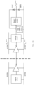
- the chip includes a power domain circuit in which a digital circuit is located and a power domain circuit in which an analog circuit is located. It is assumed that a signal cable in the power domain circuit in which the analog circuit is located is interfered with by positive static electricity. As shown in FIG. 1A , the static electricity is transmitted to a reference ground AVSS of the power domain circuit by using a diode DIOP and an ESD clamp circuit.
- a voltage of the reference ground AVSS increases. Because there are a comparatively large quantity of capacitors between a power supply AVDD of the power domain circuit and the reference ground AVSS, a voltage of the power supply AVDD increases with the voltage of the reference ground AVSS. It is also assumed that a signal cable in the power domain circuit in which the analog circuit is located is interfered with by negative static electricity. As shown in FIG. 1B , the static electricity is transmitted to the reference ground AVSS by using a diode DION. Consequently, the voltage of the reference ground AVSS decreases. When the voltage of the reference ground AVSS decreases, the voltage of the power supply AVDD decreases with the voltage of the reference ground AVSS.
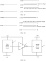
- a turnover voltage of the power domain circuit in which the analog circuit is located changes more dramatically.
- the voltage of the power supply AVDD may increase to a point A' instantaneously from a point A
- the voltage of the reference ground AVS S may increase to a point B' instantaneously from a point B. Consequently, the turnover voltage of the power domain circuit in which the analog circuit is located increases and exceeds the voltage of the power supply DVDD.
- the voltage of the power supply AVDD may decrease to a point A" instantaneously from the point A
- the voltage of the reference ground AVSS may decrease to a point B" instantaneously from the point B. Consequently, the turnover voltage of the power domain circuit in which the analog circuit is located decreases and is smaller than the voltage of the reference ground DVSS.
- the increase or the decrease of the turnover voltage of the power domain circuit in which the analog circuit is located is very likely to cause an error to a logical level of a signal transmitted by the power domain circuit in which the digital circuit is located to the power domain circuit in which the analog circuit is located.
- the signal transmitted by the power domain circuit in which the digital circuit is located to the power domain circuit in which the analog circuit is located is at a logical high level.
- a voltage of the signal is the voltage of the power supply DVDD.
- the signal is incorrectly considered to be at a logical low level in the power domain circuit in which the analog circuit is located.
- the signal transmitted by the power domain circuit in which the digital circuit is located to the power domain circuit in which the analog circuit is located is at a logical low level.
- a voltage of the signal is the voltage of the reference ground DVSS.
- the turnover voltage of the power domain circuit in which the analog circuit is located decreases and is smaller than the voltage of the reference ground DVSS due to the interference of the negative static electricity, the signal is incorrectly considered to be at a logical high level in the power domain circuit in which the analog circuit is located.
- the present invention provides an interface circuit, to correctly transmit a logical level of a signal, thereby ensuring stability and reliability of a data transmission link between power domain circuits in a chip, and improving working performance of the chip.
- voltages in the embodiments of the present invention are all determined based on a chip ground of a chip.
- a voltage of a power supply of a power domain circuit is a potential difference between the power supply of the power domain circuit and a chip ground of a chip in which the power domain circuit is located
- a voltage of a reference ground of a power domain circuit is a potential difference between the reference ground of the power domain circuit and a chip ground of a chip in which the power domain circuit is located.
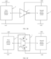
- FIG. 2A and FIG. 2B are schematic structural diagrams of an interface circuit according to an embodiment of the present invention.
- the interface circuit includes a phase inverter 1.
- the voltage of the input end 1a of the phase inverter 1 is the voltage of the reference ground vss1 of the first power domain circuit 2. In other words, the voltage of the input end 1a of the phase inverter 1 is equal to the voltage of the ground end 1d of the phase inverter 1.
- the voltage of the gate g2 of the NMOS transistor Q2 is equal to the voltage of the source s2 of the NMOS transistor Q2, and the NMOS transistor Q2 is cut off.
- a voltage, after decreasing, of the power supply vdd2 of the second power domain circuit 3 is not smaller than the voltage of the reference ground vss1 of the first power domain circuit 2
- the voltage of the gate g1 of the PMOS transistor Q1 is less than the voltage of the source s1 of the PMOS transistor Q1, and the PMOS transistor Q1 is turned on.
- the voltage of the output end 4b of the NAND gate circuit 4 is a voltage of a target power end 4c t that is in the n power ends 4c of the NAND gate circuit 4 and that is corresponding to the target input end 4at.
- the NAND gate circuit 4 is configured for transition between logical states of a signal. Specifically, the NAND gate circuit 4 is configured to: when a plurality of input signals are all at a logical high level, output a signal at a logical low level, or when any one of a plurality of input signals is at a logical low level, output a signal at a logical high level.
- the turnover voltage of the NAND gate circuit 4 is less than a first voltage of the NAND gate circuit 4 and is greater than a second voltage of the NAND gate circuit 4.
- the first voltage of the NAND gate circuit 4 is a larger voltage of the voltage of the ground end 4d of the NAND gate circuit 4 and a smallest voltage of voltages of the n power ends 4c of the NAND gate circuit 4.
- the second voltage of the NAND gate circuit 4 is a smaller voltage of the voltage of the ground end 4d of the NAND gate circuit 4 and the smallest voltage of the voltages of the n power ends 4c of the NAND gate circuit 4.
- the turnover voltage of the NAND gate circuit 4 may be half of a sum of the voltage of the ground end 4d of the NAND gate circuit 4 and the smallest voltage of the voltages of the n power ends 4c of the NAND gate circuit 4.
- the plurality of power domain circuits 5 and the target power domain circuit 6 may be different power domain circuits.
- the plurality of power domain circuits 5 and the target power domain circuit 6 use power supply solutions independent of each other, or in other words, power supply circuits of the plurality of power domain circuits 5 are different from a power supply circuit of the target power domain circuit 6.
- Each of the plurality of power domain circuits 5 may have at least one signal output end, and the plurality of power domain circuits 5 may have the n signal output ends in total.
- a voltage of a signal that is output by the power domain circuit at a logical high level is a voltage of a power supply of the power domain circuit
- a voltage of a signal that is output by the power domain circuit at a logical low level is a voltage of a reference ground of the power domain circuit.
- a voltage of the signal is a voltage of a power supply of the power domain circuit.
- a voltage of the signal is a voltage of a reference ground of the power domain circuit.
- a voltage of the i th power end 4c i of the NAND gate circuit 4 is a voltage of the power supply of the power domain circuit to which the i th signal output end 5a i belongs, and the voltage of the ground end 4d of the NAND gate circuit 4 is a voltage of the reference ground of the target power domain circuit 6.
- a voltage of an i th input end 4a i of the n input ends 4a of the NAND gate circuit 4 is the voltage of the power supply of the power domain circuit to which the i th signal output end 5a i belongs.
- the voltage of the i th input end 4a i of the NAND gate circuit 4 is equal to the voltage of the i th power end 4c i of the NAND gate circuit 4.
- a voltage of each of the n power ends 4c of the NAND gate circuit 4 is greater than the voltage of the ground end 4d of the NAND gate circuit 4, and a voltage of each of the n input ends 4a of the NAND gate circuit 4 is greater than the turnover voltage of the NAND gate circuit 4.
- the voltage of the output end 4b of the NAND gate circuit 4 is the voltage of the ground end 4d of the NAND gate circuit 4.
- a voltage of a signal transmitted by the output end 4b of the NAND gate circuit 4 to the signal input end 6a of the target power domain circuit 6 is the voltage of the reference ground of the target power domain circuit 6.
- the signal that is input to the signal input end 6a of the target power domain circuit 6 is at a logical low level in the target power domain circuit 6.
- signals that are input by the plurality of power domain circuits 5 to the NAND gate circuit 4 are all at a logical high level, and then a signal that is input by the NAND gate circuit 4 to the target power domain circuit 6 is at a logical low level, so that the logical level of the signal is correctly transmitted, thereby ensuring stability and reliability of data transmission links between the target power domain circuit 6 and the plurality of power domain circuits 5, enhancing an electrostatic interference resistance capability of a chip provided with the interface circuit, and improving working performance of the chip.
- the voltages of the n power ends 4c of the NAND gate circuit 4 are all the voltage of the power supply of the target power domain circuit 6, and the voltage of the ground end 4d of the NAND gate circuit 4 is a voltage of the reference ground of the power domain circuit to which the target signal output end 5at belongs.
- the voltage of the target input end 4at of the NAND gate circuit 4 is the voltage of the reference ground of the power domain circuit to which the target signal output end 5at belongs. In other words, the voltage of the target input end 4at of the NAND gate circuit 4 is equal to the voltage of the ground end 4d of the NAND gate circuit 4.
- the voltage of the power supply of the target power domain circuit 6 changes greatly due to electrostatic interference, provided that a voltage, after decreasing, of the power supply of the target power domain circuit 6 is not smaller than the voltage of the power supply of each of the plurality of power domain circuits 5, the voltage of each of the n power ends 4c of the NAND gate circuit 4 is greater than the voltage of the ground end 4d of the NAND gate circuit 4, and the voltage of the target input ends 4at of the NAND gate circuit 4 is smaller than the turnover voltage of the NAND gate circuit 4.
- the voltage of the output end 4b of the NAND gate circuit 4 is the voltage of the target power end 4c t that is in the n power ends 4c of the NAND gate circuit 4 and that is corresponding to the target input end 4at.
- a voltage of a signal transmitted by the output end 4b of the NAND gate circuit 4 to the signal input end 6a of the target power domain circuit 6 is the voltage of the power supply of the target power domain circuit 6.
- At least one of signals that are input by the plurality of power domain circuits 5 to the NAND gate circuit 4 is at a logical low level, and then a signal that is input by the NAND gate circuit 4 to the target power domain circuit 6 is at a logical high level, so that the logical level of the signal is correctly transmitted, thereby ensuring stability and reliability of data transmission links between the target power domain circuit 6 and the plurality of power domain circuits 5, enhancing an electrostatic interference resistance capability of a chip provided with the interface circuit, and improving working performance of the chip.
- the NAND gate circuit 4 includes n PMOS transistors Q1 and n NMOS transistors Q2.
- Both a gate g1 i of an i th PMOS transistor Q1 i of the n PMOS transistors Q1 and a gate g2 i of an i th NMOS transistor Q2 i of the n NMOS transistors Q2 are connected to the i th signal output end 5a i .
- Both a drain d1 of each of the n PMOS transistors Q1 and a drain d2 1 of a first NMOS transistor Q2 1 of the n NMOS transistors Q2 are connected to the signal input end 6a of the target power domain circuit 6.
- a source s1 i of the i th PMOS transistor Q1 i is connected to the power supply of the power domain circuit to which the i th signal output end 5a i belongs, the n NMOS transistors Q2 are connected in series, and a source s2 n of an n th NMOS transistor Q2 n of the n NMOS transistors Q2 is connected to the reference ground of the target power domain circuit 6.
- a source s1 i of the i th PMOS transistor Q1 i is connected to the power supply of the power domain circuit to which the i th signal output end 5a i belongs
- the n NMOS transistors Q2 are connected in series
- a source s2 n of an n th NMOS transistor Q2 n of the n NMOS transistors Q2 is connected to the reference ground of the target power domain circuit 6.
- a source s1 of each of the n PMOS transistors Q1 is connected to the power supply of the target power domain circuit 6, the n NMOS transistors Q2 are connected in series, and a source s2 n of an n th NMOS transistor Q2 n is connected to the reference ground of the power domain circuit to which the target signal output end 5at belongs.
- the voltage of the gate g1 i of the i th PMOS transistor Q1 i is equal to a voltage of the source s1 i of the i th PMOS transistor Q1 i , and the i th PMOS transistor Q1 i is cut off.
Landscapes
- Engineering & Computer Science (AREA)
- Computer Hardware Design (AREA)
- Physics & Mathematics (AREA)
- Computing Systems (AREA)
- General Engineering & Computer Science (AREA)
- Mathematical Physics (AREA)
- Logic Circuits (AREA)
Description
- This application relates to the field of electronic technologies, and in particular, to an interface circuit.
- With development of electronic technologies, to enable a chip to have more functions and consume less power, a plurality of power domain circuits are usually disposed in the chip. The plurality of power domain circuits use power supply solutions independent of each other, or in other words, the plurality of power domain circuits have different power supply circuits. Each power domain circuit has a turnover voltage. The turnover voltage of each power domain circuit is less than a voltage of a power supply of the power domain circuit and greater than a voltage of a reference ground of the power domain circuit. For an analog signal in a power domain circuit, if a voltage of the analog signal at a moment is greater than a turnover voltage of the power domain circuit, the analog signal is at a logical high level at this moment. If a voltage of the analog signal at a moment is smaller than the turnover voltage of the power domain circuit, the analog signal is at a logical low level at this moment. Generally, the logical high level is provided by a power supply of the power domain circuit, and the logical low level is provided by a reference ground of the power domain circuit.
- In actual application, a signal cable, a power cable, a ground cable, and the like in the chip are prone to electrostatic interference in a plugging or unplugging process or in a normal working process. The voltage of the power supply and the voltage of the reference ground of each power domain circuit in the chip change greatly due to the electrostatic interference. Consequently, the turnover voltage of each power domain circuit changes greatly. For example, when a signal cable in a power domain circuit is interfered with by positive static electricity, both a voltage of a power supply and a voltage of a reference ground of the power domain circuit increase, and consequently, a turnover voltage of the power domain circuit also increases. Alternatively, when a signal cable in a power domain circuit is interfered with by negative static electricity, both a voltage of a power supply and a voltage of a reference ground of the power domain circuit decrease, and consequently, a turnover voltage of the power domain circuit also decreases.
- In this case, if another power domain circuit transmits a signal to the power domain circuit interfered with by the static electricity, a logical level of the signal is very likely to be incorrectly transmitted. For example, a signal transmitted by a first power domain circuit to a second power domain circuit is at a logical high level. To be specific, a voltage of the signal is a voltage of a power supply of the first power domain circuit. In this case, if a turnover voltage of the second power domain circuit increases due to interference of positive static electricity and exceeds the voltage of the power supply of the first power domain circuit, the signal that is input from the first power domain circuit and that is originally at the logical high level is incorrectly considered to be at a logical low level in the second power domain circuit. For another example, a signal transmitted by the first power domain circuit to the second power domain circuit is at a logical low level. To be specific, a voltage of the signal is a voltage of a reference ground of the first power domain circuit. In this case, if a turnover voltage of the second power domain circuit decreases due to interference of negative static electricity and is smaller than the voltage of the reference ground of the first power domain circuit, the signal that is input from the first power domain circuit and that is originally at the logical low level is incorrectly considered to be at a logical high level in the second power domain circuit.
- To resolve the foregoing problem, currently, an electrostatic discharge capability is usually added to the chip. For example, an electrostatic discharge (ESD) device, such as a transient voltage suppressor (Transient Voltage Suppressor, TVS) diode or a series resistor, may be added outside the chip to directly discharge outside the chip static electricity interfering with the chip, so that the static electricity does not affect an internal circuit of the chip. Alternatively, a quantity of output pins (pin) of the ground cable in the chip may be increased to enhance an electrostatic discharge capability of the ground cable, so that a voltage of the ground cable does not become excessively high or excessively low due to electrostatic interference. However, these methods all increase packaging costs and an area of the chip, thereby affecting an application range of the chip.
-
US 2008/0204110 A1 , provides a level shift circuit for converting signals. -
US 2007/0257724 A1 , provides a level conversion circuit including a controlling section supplied with a first power supply voltage and a second power supply voltage different from each other. -
EP 3115869 A1 , discusses level-shift approaches with communication between respective circuits. - To resolve a problem in a related technology that a logical level of a signal is incorrectly transmitted, this application provides an interface circuit. The technical solutions are as follows:
- According to the invention, an interface circuit is provided as defined in
claim 1. - Normally, a voltage of the power end of the phase inverter is greater than a voltage of the ground end of the phase inverter. In this case, if a voltage of the input end of the phase inverter is greater than a turnover voltage of the phase inverter, a voltage of the output end of the phase inverter is the voltage of the ground end of the phase inverter. If a voltage of the input end of the phase inverter is less than a turnover voltage of the phase inverter, a voltage of the output end of the phase inverter is the voltage of the power end of the phase inverter. The turnover voltage of the phase inverter is a voltage between the voltage of the power end of the phase inverter and the voltage of the ground end of the phase inverter.
- It should be noted that the phase inverter is configured for transition between logical states of a signal. Specifically, the phase inverter is configured to: when an input signal is at a logical high level (that is, in a logical state "1"), output a signal at a logical low level (that is, in a logical state "0"), or when an input signal is at a logical low level, output a signal at a logical high level.
- In addition, for a power domain circuit, a voltage of a signal that is output by the power domain circuit at a logical high level is a voltage of a power supply of the power domain circuit, and a voltage of a signal that is output by the power domain circuit at a logical low level is a voltage of a reference ground of the power domain circuit.
- In this embodiment of the present invention, when the power end of the phase inverter is connected to the power supply of the first power domain circuit, and the ground end of the phase inverter is connected to the reference ground of the second power domain circuit, if a signal transmitted by the signal output end of the first power domain circuit to the input end of the phase inverter is at a logical high level, the voltage of the input end of the phase inverter is equal to the voltage of the power end of the phase inverter. Therefore, provided that a voltage, after increasing, of the reference ground of the second power domain circuit does not exceed the voltage of the power supply of the first power domain circuit, the voltage of the power end of the phase inverter is greater than the voltage of the ground end of the phase inverter, and the voltage of the input end of the phase inverter is greater than the turnover voltage of the phase inverter. In this case, the voltage of the output end of the phase inverter is the voltage of the ground end of the phase inverter. To be specific, a voltage of a signal transmitted by the output end of the phase inverter to the signal input end of the second power domain circuit is the voltage of the reference ground of the second power domain circuit. In this way, the signal that is input to the signal input end of the second power domain circuit is at a logical low level in the second power domain circuit, thereby ensuring correct transmission of the logical level of the signal.
- In addition, when the power end of the phase inverter is connected to the power supply of the second power domain circuit, and the ground end of the phase inverter is connected to the reference ground of the first power domain circuit, if a signal transmitted by the signal output end of the first power domain circuit to the input end of the phase inverter is at a logical low level, the voltage of the input end of the phase inverter is equal to the voltage of the reference ground of the phase inverter. Therefore, provided that a voltage, after decreasing, of the power supply of the second power domain circuit is not smaller than the voltage of the reference ground of the first power domain circuit, the voltage of the power end of the phase inverter is greater than the voltage of the ground end of the phase inverter, and the voltage of the input end of the phase inverter is less than the turnover voltage of the phase inverter. In this case, the voltage of the output end of the phase inverter is the voltage of the power end of the phase inverter. To be specific, a voltage of a signal transmitted by the output end of the phase inverter to the signal input end of the second power domain circuit is the voltage of the power supply of the second power domain circuit. In this way, the signal that is input to the signal input end of the second power domain circuit is at a logical high level in the second power domain circuit, thereby ensuring correct transmission of the logical level of the signal.
- The phase inverter includes a positive channel metal oxide semiconductor (positive channel Metal Oxide Semiconductor, PMOS) transistor and a negative channel metal oxide semiconductor (negative channel Metal Oxide Semiconductor, NMOS) transistor.
- Both a gate of the PMOS transistor and a gate of the NMOS transistor are connected to the signal output end of the first power domain circuit. Both a drain of the PMOS transistor and a drain of the NMOS transistor are connected to the signal input end of the second power domain circuit.
- A source of the PMOS transistor is connected to the power supply of the first power domain circuit, and a source of the NMOS transistor is connected to the reference ground of the second power domain circuit. Alternatively, a source of the PMOS transistor is connected to the power supply of the second power domain circuit, and a source of the NMOS transistor is connected to the reference ground of the first power domain circuit.
- In this embodiment of the present invention, when the source of the PMOS transistor is connected to the power supply of the first power domain circuit, and the source of the NMOS transistor is connected to the reference ground of the second power domain circuit, if a signal transmitted by the signal output end of the first power domain circuit to the input end of the phase inverter is at a logical high level, voltages applied to the gate of the PMOS transistor and the gate of the NMOS transistor are the voltage of the power supply of the first power domain circuit. In this case, the voltage of the gate of the PMOS transistor is equal to a voltage of the source of the PMOS transistor, and the PMOS transistor is cut off. When a voltage, after increasing, of the reference ground of the second power domain circuit does not exceed the voltage of the power supply of the first power domain circuit, the voltage of the gate of the NMOS transistor is greater than a voltage of the source of the NMOS transistor, and the NMOS transistor is turned on. In this way, a voltage of a connection point between the drain of the PMOS transistor and the drain of the NMOS transistor is the voltage of the reference ground of the second power domain circuit connected to the source of the NMOS transistor. To be specific, a voltage of a signal that is input to the signal input end of the second power domain circuit is the voltage of the reference ground of the second power domain circuit.
- In addition, when the source of the PMOS transistor is connected to the power supply of the second power domain circuit, and the source of the NMOS transistor is connected to the reference ground of the first power domain circuit, if a signal transmitted by the signal output end of the first power domain circuit to the input end of the phase inverter is at a logical low level, voltages applied to the gate of the PMOS transistor and the gate of the NMOS transistor are the voltage of the reference ground of the first power domain circuit. In this case, the voltage of the gate of the NMOS transistor is equal to the voltage of the source of the NMOS transistor, and the NMOS transistor is cut off. When a voltage, after decreasing, of the power supply of the second power domain circuit is not smaller than the voltage of the reference ground of the first power domain circuit, the voltage of the gate of the PMOS transistor is less than the voltage of the source of the PMOS transistor, and the PMOS transistor is turned on. In this way, the voltage of the connection point between the drain of the PMOS transistor and the drain of the NMOS transistor is the voltage of the power supply of the second power domain circuit connected to the source of the PMOS transistor. To be specific, a voltage of a signal that is input to the signal input end of the second power domain circuit is the voltage of the power supply of the second power domain circuit.
- Beneficial effects brought by the technical solutions provided in this application are as follows: The input end of the phase inverter is connected to the signal output end of the first power domain circuit, and the output end of the phase inverter is connected to the signal input end of the second power domain circuit. In this case, if the power end of the phase inverter is connected to the power supply of the first power domain circuit, and the ground end of the phase inverter is connected to the reference ground of the second power domain circuit, when a signal transmitted by the signal output end of the first power domain circuit to the input end of the phase inverter is at a logical high level, the voltage of the input end of the phase inverter is equal to the voltage of the power end of the phase inverter. Therefore, even if the voltage of the reference ground of the second power domain circuit changes greatly due to electrostatic interference, provided that a voltage, after increasing, of the reference ground of the second power domain circuit does not exceed the voltage of the power supply of the first power domain circuit, the voltage of the power end of the phase inverter is greater than the voltage of the ground end of the phase inverter, and the voltage of the input end of the phase inverter is greater than the turnover voltage of the phase inverter. In this case, a voltage of a signal transmitted by the output end of the phase inverter to the signal input end of the second power domain circuit is the voltage of the reference ground of the second power domain circuit. In this way, the signal that is input to the signal input end of the second power domain circuit is at a logical low level in the second power domain circuit, thereby ensuring correct transmission of the logical level of the signal. If the power end of the phase inverter is connected to the power supply of the second power domain circuit, and the ground end of the phase inverter is connected to the reference ground of the first power domain circuit, when a signal transmitted by the signal output end of the first power domain circuit to the input end of the phase inverter is at a logical low level, the voltage of the input end of the phase inverter is equal to the voltage of the reference ground of the phase inverter. Therefore, even if the voltage of the power supply of the second power domain circuit changes greatly due to electrostatic interference, provided that a voltage, after decreasing, of the power supply of the second power domain circuit is not smaller than the voltage of the reference ground of the first power domain circuit, the voltage of the power end of the phase inverter is greater than the voltage of the ground end of the phase inverter, and the voltage of the input end of the phase inverter is less than the turnover voltage of the phase inverter. In this case, a voltage of a signal transmitted by the output end of the phase inverter to the signal input end of the second power domain circuit is the voltage of the power supply of the second power domain circuit. In this way, the signal that is input to the signal input end of the second power domain circuit is at a logical high level in the second power domain circuit, thereby ensuring correct transmission of the logical level of the signal.
-
-
FIG. 1A is a schematic diagram of a power domain circuit interfered with by positive static electricity according to an embodiment of the present invention; -
FIG. 1B is a schematic diagram of a power domain circuit interfered with by negative static electricity according to an embodiment of the present invention; -
FIG. 1C is a schematic diagram of voltage increases of a power supply and a reference ground according to an embodiment of the present invention; -
FIG. 1D is a schematic diagram of voltage decreases of a power supply and a reference ground according to an embodiment of the present invention; -
FIG. 2A is a schematic structural diagram of a first interface circuit according to an embodiment of the present invention; -
FIG. 2B is a schematic structural diagram of a second interface circuit according to an embodiment of the present invention; -
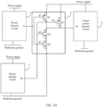
FIG. 2C is a schematic structural diagram of a third interface circuit according to an embodiment of the present invention; -
FIG. 2D is a schematic structural diagram of a fourth interface circuit according to an embodiment of the present invention; -
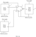
FIG. 3A is a schematic structural diagram of a fifth interface circuit according to an example not covered by the invention; -
FIG. 3B is a schematic structural diagram of a sixth interface circuit according to an example not covered by the invention; -
FIG. 3C is a schematic structural diagram of a seventh interface circuit according to an example not covered by the invention; -
FIG. 3D is a schematic structural diagram of an eighth interface circuit according to an example not covered by the invention; -
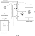
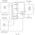
FIG. 4A is a schematic structural diagram of a ninth interface circuit according to an example not covered by the invention; -
FIG. 4B is a schematic structural diagram of a tenth interface circuit according to an example not covered by the invention; -
FIG. 4C is a schematic structural diagram of an eleventh interface circuit according to an example not covered by the invention; and -
FIG. 4D is a schematic structural diagram of a twelfth interface circuit according to an example not covered by the invention. -
- 1: phase inverter; 1a: input end of the phase inverter; 1b: output end of the phase inverter; 1c: power end of the phase inverter; 1d: ground end of the phase inverter; 2: first power domain circuit; 2a: signal output end of the first power domain circuit; vdd1: power supply of the first power domain circuit; vss1: reference ground of the first power domain circuit; 3: second power domain circuit; 3a: signal input end of the second power domain circuit; vdd2: power supply of the second power domain circuit; vss2: reference ground of the second power domain circuit;
- 4: NAND gate circuit; 4a: input end of the NAND gate circuit; 4at: target input end of the NAND gate circuit; 4b: output end of the NAND gate circuit; 4c: power end of the NAND gate circuit; 4ct: target power end of the NAND gate circuit; 4d: ground end of the NAND gate circuit; 5: power domain circuit; 5a: signal output end of the power domain circuit; 5at: target signal output end of the power domain circuit; 6: target power domain circuit; 6a: signal input end of the target power domain circuit; 7: NOR gate circuit; 7a: input end of the NOR gate circuit; 7at: target input end of the NOR gate circuit; 7b: output end of the NOR gate circuit; 7c: power end of the NOR gate circuit; 7d: ground end of the NOR gate circuit; 7dt: target ground end of the NOR gate circuit;
- Q1: PMOS transistor; g1: gate of the PMOS transistor; s1: source of the PMOS transistor; d1: drain of the PMOS transistor; Q1t: target PMOS transistor; g1t: gate of the target PMOS transistor; s1t: source of the target PMOS transistor; d1t: drain of the target PMOS transistor; Q2: NMOS transistor; g2: gate of the NMOS transistor; s2: source of the NMOS transistor; d2: drain of the NMOS; Q2t: target NMOS transistor; g2t: gate of the target NMOS transistor; s2t: source of the target NMOS transistor; d2t: drain of the target NMOS transistor.
- To make the objectives, technical solutions, and advantages of this application clearer, the following further describes the implementations of this application in detail with reference to the accompanying drawings.
- Before the embodiments of the present invention are described in detail, an application scenario of the embodiments of the present invention is described.
- Currently, a signal cable, a power cable, a ground cable, and the like in a chip are prone to electrostatic interference in a plugging or unplugging process or in a normal working process. A voltage of a power supply and a voltage of a reference ground of each power domain circuit in the chip change greatly due to the electrostatic interference. For example, the chip includes a power domain circuit in which a digital circuit is located and a power domain circuit in which an analog circuit is located. It is assumed that a signal cable in the power domain circuit in which the analog circuit is located is interfered with by positive static electricity. As shown in
FIG. 1A , the static electricity is transmitted to a reference ground AVSS of the power domain circuit by using a diode DIOP and an ESD clamp circuit. Consequently, a voltage of the reference ground AVSS increases. Because there are a comparatively large quantity of capacitors between a power supply AVDD of the power domain circuit and the reference ground AVSS, a voltage of the power supply AVDD increases with the voltage of the reference ground AVSS. It is also assumed that a signal cable in the power domain circuit in which the analog circuit is located is interfered with by negative static electricity. As shown inFIG. 1B , the static electricity is transmitted to the reference ground AVSS by using a diode DION. Consequently, the voltage of the reference ground AVSS decreases. When the voltage of the reference ground AVSS decreases, the voltage of the power supply AVDD decreases with the voltage of the reference ground AVSS. - In this case, compared with a voltage of a power supply DVDD and a voltage of a reference ground DVSS of the power domain circuit in which the digital circuit is located, a turnover voltage of the power domain circuit in which the analog circuit is located changes more dramatically. For example, when the power domain circuit in which the analog circuit is located is interfered with by the positive static electricity in
FIG. 1A , as shown inFIG. 1C , the voltage of the power supply AVDD may increase to a point A' instantaneously from a point A, and the voltage of the reference ground AVS S may increase to a point B' instantaneously from a point B. Consequently, the turnover voltage of the power domain circuit in which the analog circuit is located increases and exceeds the voltage of the power supply DVDD. For another example, when the power domain circuit in which the analog circuit is located is interfered with by the negative static electricity inFIG. 1B , as shown inFIG. 1D , the voltage of the power supply AVDD may decrease to a point A" instantaneously from the point A, and the voltage of the reference ground AVSS may decrease to a point B" instantaneously from the point B. Consequently, the turnover voltage of the power domain circuit in which the analog circuit is located decreases and is smaller than the voltage of the reference ground DVSS. - The increase or the decrease of the turnover voltage of the power domain circuit in which the analog circuit is located is very likely to cause an error to a logical level of a signal transmitted by the power domain circuit in which the digital circuit is located to the power domain circuit in which the analog circuit is located. For example, the signal transmitted by the power domain circuit in which the digital circuit is located to the power domain circuit in which the analog circuit is located is at a logical high level. To be specific, a voltage of the signal is the voltage of the power supply DVDD. In this case, if the turnover voltage of the power domain circuit in which the analog circuit is located increases and exceeds the voltage of the power supply DVDD due to the interference of the positive static electricity, the signal is incorrectly considered to be at a logical low level in the power domain circuit in which the analog circuit is located. For another example, the signal transmitted by the power domain circuit in which the digital circuit is located to the power domain circuit in which the analog circuit is located is at a logical low level. To be specific, a voltage of the signal is the voltage of the reference ground DVSS. In this case, if the turnover voltage of the power domain circuit in which the analog circuit is located decreases and is smaller than the voltage of the reference ground DVSS due to the interference of the negative static electricity, the signal is incorrectly considered to be at a logical high level in the power domain circuit in which the analog circuit is located.
- It can be learned from the foregoing that when a signal transmitted by a power domain circuit to another power domain circuit that is interfered with by positive static electricity is at a logical high level, the logical level of the signal is very likely to be incorrectly transmitted at a logical low level; and when a signal transmitted by a power domain circuit to another power domain circuit that is interfered with by negative static electricity is at a logical low level, the logical level of the signal is very likely to be incorrectly transmitted at a logical high level. Incorrect transmission of a logical level of a signal is very likely to cause an incorrect change in internal state logic or a state of some registers in a power domain circuit receiving the signal. This causes an error to a data transmission link between power domain circuits in a chip, and affects working performance of the chip. Therefore, the present invention provides an interface circuit, to correctly transmit a logical level of a signal, thereby ensuring stability and reliability of a data transmission link between power domain circuits in a chip, and improving working performance of the chip.
- It should be noted that voltages in the embodiments of the present invention are all determined based on a chip ground of a chip. For example, a voltage of a power supply of a power domain circuit is a potential difference between the power supply of the power domain circuit and a chip ground of a chip in which the power domain circuit is located, and a voltage of a reference ground of a power domain circuit is a potential difference between the reference ground of the power domain circuit and a chip ground of a chip in which the power domain circuit is located.
- The following describes in detail a first interface circuit provided in an embodiment of the present invention.
-
FIG. 2A andFIG. 2B are schematic structural diagrams of an interface circuit according to an embodiment of the present invention. Referring toFIG. 2A andFIG. 2B , the interface circuit includes aphase inverter 1. - An input end 1a of the
phase inverter 1 is connected to asignal output end 2a of a firstpower domain circuit 2, and anoutput end 1b of thephase inverter 1 is connected to a signal input end 3a of a secondpower domain circuit 3. - Referring to
FIG. 2A , a power end 1c of thephase inverter 1 is connected to a power supply vdd1 of the firstpower domain circuit 2, and aground end 1d of thephase inverter 1 is connected to a reference ground vss2 of the secondpower domain circuit 3. Alternatively, referring toFIG. 2B , a power end 1c of thephase inverter 1 is connected to a power supply vdd2 of the secondpower domain circuit 3, and aground end 1d of thephase inverter 1 is connected to a reference ground vss1 of the firstpower domain circuit 2. - Normally, a voltage of the power end 1c of the
phase inverter 1 is greater than a voltage of theground end 1d of thephase inverter 1. In this case, if a voltage of the input end 1a of thephase inverter 1 is greater than a turnover voltage of thephase inverter 1, a voltage of theoutput end 1b of thephase inverter 1 is the voltage of theground end 1d of thephase inverter 1. If a voltage of the input end 1a of thephase inverter 1 is less than a turnover voltage of thephase inverter 1, a voltage of theoutput end 1b of thephase inverter 1 is the voltage of the power end 1c of thephase inverter 1. - It should be noted that the
phase inverter 1 is configured for transition between logical states of a signal. Specifically, thephase inverter 1 is configured to: when an input signal is at a logical high level (that is, in a logical state "1"), output a signal at a logical low level (that is, in a logical state "0"), or when an input signal is at a logical low level, output a signal at a logical high level. - In addition, the turnover voltage of the
phase inverter 1 is less than a first voltage of thephase inverter 1 and is greater than a second voltage of thephase inverter 1. The first voltage of thephase inverter 1 is a larger voltage of the voltage of the power end 1c of thephase inverter 1 and the voltage of theground end 1d of thephase inverter 1. The second voltage of thephase inverter 1 is a smaller voltage of the voltage of the power end 1c of thephase inverter 1 and the voltage of theground end 1d of thephase inverter 1. For example, the turnover voltage of thephase inverter 1 may be half of a sum of the voltage of the power end 1c of thephase inverter 1 and the voltage of theground end 1d of thephase inverter 1. - It should be noted that the first
power domain circuit 2 and the secondpower domain circuit 3 may be two different power domain circuits. To be specific, the firstpower domain circuit 2 and the secondpower domain circuit 3 use power supply solutions independent of each other, or in other words, a power supply circuit of the firstpower domain circuit 2 is different from a power supply circuit of the secondpower domain circuit 3. - In addition, for a power domain circuit, a voltage of a signal that is output by the power domain circuit at a logical high level is a voltage of a power supply of the power domain circuit, and a voltage of a signal that is output by the power domain circuit at a logical low level is a voltage of a reference ground of the power domain circuit. For example, if a signal that is output by the first
power domain circuit 2 is at a logical high level, a voltage of the signal is a voltage of the power supply vdd1 of the firstpower domain circuit 2. For another example, if a signal that is output by the firstpower domain circuit 2 is at a logical low level, a voltage of the signal is a voltage of the reference ground vss1 of the firstpower domain circuit 2. - It should be noted that when the power end 1c of the
phase inverter 1 is connected to the power supply vdd1 of the firstpower domain circuit 2, and theground end 1d of thephase inverter 1 is connected to the reference ground vss2 of the secondpower domain circuit 3, the voltage of the power end 1c of thephase inverter 1 is the voltage of the power supply vdd1 of the firstpower domain circuit 2, and the voltage of theground end 1d of thephase inverter 1 is a voltage of the reference ground vss2 of the secondpower domain circuit 3. In this case, when a signal transmitted by thesignal output end 2a of the firstpower domain circuit 2 to the input end 1a of thephase inverter 1 is at a logical high level, the voltage of the input end 1a of thephase inverter 1 is the voltage of the power supply vdd1 of the firstpower domain circuit 2. In other words, the voltage of the input end 1a of thephase inverter 1 is equal to the voltage of the power end 1c of thephase inverter 1. Therefore, even if the voltage of the reference ground vss2 of the secondpower domain circuit 3 changes greatly due to electrostatic interference, provided that a voltage, after increasing, of the reference ground vss2 of the secondpower domain circuit 3 does not exceed the voltage of the power supply vdd1 of the firstpower domain circuit 2, the voltage of the power end 1c of thephase inverter 1 is greater than the voltage of theground end 1d of thephase inverter 1, and the voltage of the input end 1a of thephase inverter 1 is greater than the turnover voltage of thephase inverter 1. In this case, the voltage of theoutput end 1b of thephase inverter 1 is the voltage of theground end 1d of thephase inverter 1. To be specific, a voltage of a signal transmitted by theoutput end 1b of thephase inverter 1 to the signal input end 3a of the secondpower domain circuit 3 is the voltage of the reference ground vss2 of the secondpower domain circuit 3. - When the voltage of the signal transmitted by the
output end 1b of thephase inverter 1 to the signal input end 3a of the secondpower domain circuit 3 is the voltage of the reference ground vss2 of the secondpower domain circuit 3, the signal that is input to the signal input end 3a of the secondpower domain circuit 3 is at a logical low level in the secondpower domain circuit 3. In this case, a signal that is input by the firstpower domain circuit 2 to thephase inverter 1 is at a logical high level, and then a signal that is input by thephase inverter 1 to the secondpower domain circuit 3 is at a logical low level, so that the logical level of the signal is correctly transmitted, thereby ensuring stability and reliability of a data transmission link between the firstpower domain circuit 2 and the secondpower domain circuit 3, enhancing an electrostatic interference resistance capability of a chip provided with the interface circuit, and improving working performance of the chip. - In addition, when the power end 1c of the
phase inverter 1 is connected to the power supply vdd2 of the secondpower domain circuit 3, and theground end 1d of thephase inverter 1 is connected to the reference ground vss1 of the firstpower domain circuit 2, the voltage of the power end 1c of thephase inverter 1 is the voltage of the power supply vdd2 of the secondpower domain circuit 3, and the voltage of theground end 1d of thephase inverter 1 is the voltage of the reference ground vss1 of the firstpower domain circuit 2. In this case, when a signal transmitted by thesignal output end 2a of the firstpower domain circuit 2 to the input end 1a of thephase inverter 1 is at a logical low level, the voltage of the input end 1a of thephase inverter 1 is the voltage of the reference ground vss1 of the firstpower domain circuit 2. In other words, the voltage of the input end 1a of thephase inverter 1 is equal to the voltage of theground end 1d of thephase inverter 1. Therefore, even if the voltage of the power supply vdd2 of the secondpower domain circuit 3 changes greatly due to electrostatic interference, provided that a voltage, after decreasing, of the power supply vdd2 of the secondpower domain circuit 3 is not smaller than the voltage of the reference ground vss1 of the firstpower domain circuit 2, the voltage of the power end 1c of thephase inverter 1 is greater than the voltage of theground end 1d of thephase inverter 1, and the voltage of the input end 1a of thephase inverter 1 is less than the turnover voltage of thephase inverter 1. In this case, the voltage of theoutput end 1b of thephase inverter 1 is the voltage of the power end 1c of thephase inverter 1. To be specific, a voltage of a signal transmitted by theoutput end 1b of thephase inverter 1 to the signal input end 3a of the secondpower domain circuit 3 is the voltage of the power supply vdd2 of the secondpower domain circuit 3. - When the voltage of the signal transmitted by the
output end 1b of thephase inverter 1 to the signal input end 3a of the secondpower domain circuit 3 is the voltage of the power supply vdd2 of the secondpower domain circuit 3, the signal that is input to the signal input end 3a of the secondpower domain circuit 3 is at a logical high level in the secondpower domain circuit 3. In this case, a signal that is input by the firstpower domain circuit 2 to thephase inverter 1 is at a logical low level, and then a signal that is input by thephase inverter 1 to the secondpower domain circuit 3 is at a logical high level, so that the logical level of the signal is correctly transmitted, thereby ensuring stability and reliability of a data transmission link between the firstpower domain circuit 2 and the secondpower domain circuit 3, enhancing an electrostatic interference resistance capability of a chip provided with the interface circuit, and improving working performance of the chip. - Referring to
FIG. 2C andFIG. 2D , thephase inverter 1 includes a PMOS transistor Q1 and an NMOS transistor Q2. - Both a gate g1 of the PMOS transistor Q1 and a gate g2 of the NMOS transistor Q2 are connected to the
signal output end 2a of the firstpower domain circuit 2. Both a drain d1 of the PMOS transistor Q1 and a drain d2 of the NMOS transistor Q2 are connected to the signal input end 3a of the secondpower domain circuit 3. - Referring to
FIG. 2C , a source s1 of the PMOS transistor Q1 is connected to the power supply vdd1 of the firstpower domain circuit 2, and a source s2 of the NMOS transistor Q2 is connected to the reference ground vss2 of the secondpower domain circuit 3. Alternatively, referring toFIG. 2D , a source s1 of the PMOS transistor Q1 is connected to the power supply vdd2 of the secondpower domain circuit 3, and a source s2 of the NMOS transistor Q2 is connected to the reference ground vss1 of the firstpower domain circuit 2. - It should be noted that when the source s1 of the PMOS transistor Q1 is connected to the power supply vdd1 of the first
power domain circuit 2, and the source s2 of the NMOS transistor Q2 is connected to the reference ground vss2 of the secondpower domain circuit 3, if a signal transmitted by thesignal output end 2a of the firstpower domain circuit 2 to the input end 1a of thephase inverter 1 is at a logical high level, voltages applied to the gate g1 of the PMOS transistor Q1 and the gate g2 of the NMOS transistor Q2 are the voltage of the power supply vdd1 of the firstpower domain circuit 2. In this case, the voltage of the gate g1 of the PMOS transistor Q1 is equal to a voltage of the source s1 of the PMOS transistor Q1, and the PMOS transistor Q1 is cut off. When a voltage, after increasing, of the reference ground vss2 of the secondpower domain circuit 3 does not exceed the voltage of the power supply vdd1 of the firstpower domain circuit 2, the voltage of the gate g2 of the NMOS transistor Q2 is greater than a voltage of the source s2 of the NMOS transistor Q2, and the NMOS transistor Q2 is turned on. In this way, a voltage of a connection point between the drain d1 of the PMOS transistor Q1 and the drain d2 of the NMOS transistor Q2 is the voltage of the reference ground vss2 of the secondpower domain circuit 3 connected to the source s2 of the NMOS transistor Q2. To be specific, a voltage of a signal that is input to the signal input end 3a of the secondpower domain circuit 3 is the voltage of the reference ground vss2 of the secondpower domain circuit 3. - In addition, when the source s1 of the PMOS transistor Q1 is connected to the power supply vdd2 of the second
power domain circuit 3, and the source s2 of the NMOS transistor Q2 is connected to the reference ground vss1 of the firstpower domain circuit 2, if a signal transmitted by thesignal output end 2a of the firstpower domain circuit 2 to the input end 1a of thephase inverter 1 is at a logical low level, voltages applied to the gate g1 of the PMOS transistor Q1 and the gate g2 of the NMOS transistor Q2 are the voltage of the reference ground vss1 of the firstpower domain circuit 2. In this case, the voltage of the gate g2 of the NMOS transistor Q2 is equal to the voltage of the source s2 of the NMOS transistor Q2, and the NMOS transistor Q2 is cut off. When a voltage, after decreasing, of the power supply vdd2 of the secondpower domain circuit 3 is not smaller than the voltage of the reference ground vss1 of the firstpower domain circuit 2, the voltage of the gate g1 of the PMOS transistor Q1 is less than the voltage of the source s1 of the PMOS transistor Q1, and the PMOS transistor Q1 is turned on. In this way, the voltage of the connection point between the drain d1 of the PMOS transistor Q1 and the drain d2 of the NMOS transistor Q2 is the voltage of the power supply vdd2 of the secondpower domain circuit 3 connected to the source s1 of the PMOS transistor Q1. To be specific, a voltage of a signal that is input to the signal input end 3a of the secondpower domain circuit 3 is the voltage of the power supply vdd2 of the secondpower domain circuit 3. - In this embodiment of the present invention, the input end of the phase inverter is connected to the signal output end of the first power domain circuit, and the output end of the phase inverter is connected to the signal input end of the second power domain circuit. In this case, if the power end of the phase inverter is connected to the power supply of the first power domain circuit, and the ground end of the phase inverter is connected to the reference ground of the second power domain circuit, when a signal transmitted by the signal output end of the first power domain circuit to the input end of the phase inverter is at a logical high level, the voltage of the input end of the phase inverter is equal to the voltage of the power end of the phase inverter. Therefore, even if the voltage of the reference ground of the second power domain circuit changes greatly due to electrostatic interference, provided that a voltage, after increasing, of the reference ground of the second power domain circuit does not exceed the voltage of the power supply of the first power domain circuit, the voltage of the power end of the phase inverter is greater than the voltage of the ground end of the phase inverter, and the voltage of the input end of the phase inverter is greater than the turnover voltage of the phase inverter. In this case, a voltage of a signal transmitted by the output end of the phase inverter to the signal input end of the second power domain circuit is the voltage of the reference ground of the second power domain circuit. In this way, the signal that is input to the signal input end of the second power domain circuit is at a logical low level in the second power domain circuit, thereby ensuring correct transmission of the logical level of the signal. If the power end of the phase inverter is connected to the power supply of the second power domain circuit, and the ground end of the phase inverter is connected to the reference ground of the first power domain circuit, when a signal transmitted by the signal output end of the first power domain circuit to the input end of the phase inverter is at a logical low level, the voltage of the input end of the phase inverter is equal to the voltage of the reference ground of the phase inverter. Therefore, even if the voltage of the power supply of the second power domain circuit changes greatly due to electrostatic interference, provided that a voltage, after decreasing, of the power supply of the second power domain circuit is not smaller than the voltage of the reference ground of the first power domain circuit, the voltage of the power end of the phase inverter is greater than the voltage of the ground end of the phase inverter, and the voltage of the input end of the phase inverter is less than the turnover voltage of the phase inverter. In this case, a voltage of a signal transmitted by the output end of the phase inverter to the signal input end of the second power domain circuit is the voltage of the power supply of the second power domain circuit. In this way, the signal that is input to the signal input end of the second power domain circuit is at a logical high level in the second power domain circuit, thereby ensuring correct transmission of the logical level of the signal.
- The following describes in detail a second interface circuit provided in an embodiment of the present invention.
-
FIG. 3A andFIG. 3B are schematic structural diagrams of an interface circuit according to an example not covered by the invention. Referring toFIG. 3A andFIG. 3B , the interface circuit includes aNAND gate circuit 4. - n input ends 4a of the
NAND gate circuit 4 are respectively connected to n signal output ends 5a of a plurality ofpower domain circuits 5, and anoutput end 4b of theNAND gate circuit 4 is connected to asignal input end 6a of a targetpower domain circuit 6. The n input ends 4a of theNAND gate circuit 4 one-to-one correspond to n power ends 4c of theNAND gate circuit 4, and n is an integer greater than or equal to 2. - Referring to
FIG. 3A , an ith power end 4ci of the n power ends 4c of theNAND gate circuit 4 is connected to a power supply of a power domain circuit to which an ithsignal output end 5ai of the n signal output ends 5a belongs, aground end 4d of theNAND gate circuit 4 is connected to a reference ground of the targetpower domain circuit 6, and i is an integer greater than or equal to 1 and less than or equal to n. Alternatively, referring toFIG. 3B , the n power ends 4c of theNAND gate circuit 4 are all connected to a power supply of the targetpower domain circuit 6, and aground end 4d of theNAND gate circuit 4 is connected to a reference ground of a power domain circuit to which a target signal output end 5at of the n signal output ends 5a belongs, and the targetsignal output end 5at is connected to a target input end 4at of the n input ends 4a of theNAND gate circuit 4. - Normally, a voltage of each of the n power ends 4c of the
NAND gate circuit 4 is greater than a voltage of theground end 4d of theNAND gate circuit 4. In this case, if a voltage of each of the n input ends 4a of theNAND gate circuit 4 is greater than a turnover voltage of theNAND gate circuit 4, a voltage of theoutput end 4b of theNAND gate circuit 4 is the voltage of theground end 4d of theNAND gate circuit 4. If a voltage of the target input end 4at of theNAND gate circuit 4 is less than the turnover voltage of theNAND gate circuit 4, the voltage of theoutput end 4b of theNAND gate circuit 4 is a voltage of atarget power end 4ct that is in the n power ends 4c of theNAND gate circuit 4 and that is corresponding to the target input end 4at. - It should be noted that the
NAND gate circuit 4 is configured for transition between logical states of a signal. Specifically, theNAND gate circuit 4 is configured to: when a plurality of input signals are all at a logical high level, output a signal at a logical low level, or when any one of a plurality of input signals is at a logical low level, output a signal at a logical high level. - In addition, the turnover voltage of the
NAND gate circuit 4 is less than a first voltage of theNAND gate circuit 4 and is greater than a second voltage of theNAND gate circuit 4. The first voltage of theNAND gate circuit 4 is a larger voltage of the voltage of theground end 4d of theNAND gate circuit 4 and a smallest voltage of voltages of the n power ends 4c of theNAND gate circuit 4. The second voltage of theNAND gate circuit 4 is a smaller voltage of the voltage of theground end 4d of theNAND gate circuit 4 and the smallest voltage of the voltages of the n power ends 4c of theNAND gate circuit 4. For example, the turnover voltage of theNAND gate circuit 4 may be half of a sum of the voltage of theground end 4d of theNAND gate circuit 4 and the smallest voltage of the voltages of the n power ends 4c of theNAND gate circuit 4. - It should be noted that the plurality of
power domain circuits 5 and the targetpower domain circuit 6 may be different power domain circuits. To be specific, the plurality ofpower domain circuits 5 and the targetpower domain circuit 6 use power supply solutions independent of each other, or in other words, power supply circuits of the plurality ofpower domain circuits 5 are different from a power supply circuit of the targetpower domain circuit 6. Each of the plurality ofpower domain circuits 5 may have at least one signal output end, and the plurality ofpower domain circuits 5 may have the n signal output ends in total. - In addition, for a power domain circuit, a voltage of a signal that is output by the power domain circuit at a logical high level is a voltage of a power supply of the power domain circuit, and a voltage of a signal that is output by the power domain circuit at a logical low level is a voltage of a reference ground of the power domain circuit. For example, if a signal that is output by any one of the plurality of
power domain circuits 5 is at a logical high level, a voltage of the signal is a voltage of a power supply of the power domain circuit. For another example, if a signal that is output by any one of the plurality ofpower domain circuits 5 is at a logical low level, a voltage of the signal is a voltage of a reference ground of the power domain circuit. - It should be noted that when the ith power end 4ci of the n power ends 4c of the
NAND gate circuit 4 is connected to the power supply of the power domain circuit to which the ithsignal output end 5ai of the n signal output ends 5a belongs, and theground end 4d of theNAND gate circuit 4 is connected to the reference ground of the targetpower domain circuit 6, a voltage of the ithpower end 4ci of theNAND gate circuit 4 is a voltage of the power supply of the power domain circuit to which the ithsignal output end 5ai belongs, and the voltage of theground end 4d of theNAND gate circuit 4 is a voltage of the reference ground of the targetpower domain circuit 6. In this case, when signals transmitted by the n signal output ends 5a to the n input ends 4a of theNAND gate circuit 4 are all at a logical high level, a voltage of an ithinput end 4ai of the n input ends 4a of theNAND gate circuit 4 is the voltage of the power supply of the power domain circuit to which the ithsignal output end 5ai belongs. In other words, the voltage of the ithinput end 4ai of theNAND gate circuit 4 is equal to the voltage of the ithpower end 4ci of theNAND gate circuit 4. Therefore, even if the voltage of the reference ground of the targetpower domain circuit 6 changes greatly due to electrostatic interference, provided that a voltage, after increasing, of the reference ground of the targetpower domain circuit 6 does not exceed a voltage of a power supply of each of the plurality ofpower domain circuits 5, a voltage of each of the n power ends 4c of theNAND gate circuit 4 is greater than the voltage of theground end 4d of theNAND gate circuit 4, and a voltage of each of the n input ends 4a of theNAND gate circuit 4 is greater than the turnover voltage of theNAND gate circuit 4. In this case, the voltage of theoutput end 4b of theNAND gate circuit 4 is the voltage of theground end 4d of theNAND gate circuit 4. To be specific, a voltage of a signal transmitted by theoutput end 4b of theNAND gate circuit 4 to thesignal input end 6a of the targetpower domain circuit 6 is the voltage of the reference ground of the targetpower domain circuit 6. - When the voltage of the signal transmitted by the
output end 4b of theNAND gate circuit 4 to thesignal input end 6a of the targetpower domain circuit 6 is the voltage of the reference ground of the targetpower domain circuit 6, the signal that is input to thesignal input end 6a of the targetpower domain circuit 6 is at a logical low level in the targetpower domain circuit 6. In this case, signals that are input by the plurality ofpower domain circuits 5 to theNAND gate circuit 4 are all at a logical high level, and then a signal that is input by theNAND gate circuit 4 to the targetpower domain circuit 6 is at a logical low level, so that the logical level of the signal is correctly transmitted, thereby ensuring stability and reliability of data transmission links between the targetpower domain circuit 6 and the plurality ofpower domain circuits 5, enhancing an electrostatic interference resistance capability of a chip provided with the interface circuit, and improving working performance of the chip. - In addition, when the n power ends 4c of the
NAND gate circuit 4 are all connected to the power supply of the targetpower domain circuit 6, and theground end 4d of theNAND gate circuit 4 is connected to the reference ground of the power domain circuit to which the target signal output end 5at of the n signal output ends 5a belongs, the voltages of the n power ends 4c of theNAND gate circuit 4 are all the voltage of the power supply of the targetpower domain circuit 6, and the voltage of theground end 4d of theNAND gate circuit 4 is a voltage of the reference ground of the power domain circuit to which the target signal output end 5at belongs. In this case, when a signal transmitted by the target signal output end 5at of the n signal output ends 5a to the target input end 4at of the n input ends 4a of theNAND gate circuit 4 is at a logical low level, the voltage of the target input end 4at of theNAND gate circuit 4 is the voltage of the reference ground of the power domain circuit to which the target signal output end 5at belongs. In other words, the voltage of the target input end 4at of theNAND gate circuit 4 is equal to the voltage of theground end 4d of theNAND gate circuit 4. Therefore, even if the voltage of the power supply of the targetpower domain circuit 6 changes greatly due to electrostatic interference, provided that a voltage, after decreasing, of the power supply of the targetpower domain circuit 6 is not smaller than the voltage of the power supply of each of the plurality ofpower domain circuits 5, the voltage of each of the n power ends 4c of theNAND gate circuit 4 is greater than the voltage of theground end 4d of theNAND gate circuit 4, and the voltage of the target input ends 4at of theNAND gate circuit 4 is smaller than the turnover voltage of theNAND gate circuit 4. In this case, the voltage of theoutput end 4b of theNAND gate circuit 4 is the voltage of thetarget power end 4ct that is in the n power ends 4c of theNAND gate circuit 4 and that is corresponding to the target input end 4at. To be specific, a voltage of a signal transmitted by theoutput end 4b of theNAND gate circuit 4 to thesignal input end 6a of the targetpower domain circuit 6 is the voltage of the power supply of the targetpower domain circuit 6. - When the voltage of the signal transmitted by the
output end 4b of theNAND gate circuit 4 to thesignal input end 6a of the targetpower domain circuit 6 is the voltage of the power supply of the targetpower domain circuit 6, the signal that is input to thesignal input end 6a of the targetpower domain circuit 6 is at a logical high level in the targetpower domain circuit 6. In this case, at least one of signals that are input by the plurality ofpower domain circuits 5 to theNAND gate circuit 4 is at a logical low level, and then a signal that is input by theNAND gate circuit 4 to the targetpower domain circuit 6 is at a logical high level, so that the logical level of the signal is correctly transmitted, thereby ensuring stability and reliability of data transmission links between the targetpower domain circuit 6 and the plurality ofpower domain circuits 5, enhancing an electrostatic interference resistance capability of a chip provided with the interface circuit, and improving working performance of the chip. - Referring to
FIG. 3C andFIG. 3D , theNAND gate circuit 4 includes n PMOS transistors Q1 and n NMOS transistors Q2. - Both a gate g1i of an ith PMOS transistor Q1i of the n PMOS transistors Q1 and a gate g2i of an ith NMOS transistor Q2i of the n NMOS transistors Q2 are connected to the ith
signal output end 5ai. Both a drain d1 of each of the n PMOS transistors Q1 and a drain d21 of a first NMOS transistor Q21 of the n NMOS transistors Q2 are connected to thesignal input end 6a of the targetpower domain circuit 6. - Referring to
FIG. 3C , a source s1i of the ith PMOS transistor Q1i is connected to the power supply of the power domain circuit to which the ithsignal output end 5ai belongs, the n NMOS transistors Q2 are connected in series, and a source s2n of an nth NMOS transistor Q2n of the n NMOS transistors Q2 is connected to the reference ground of the targetpower domain circuit 6. Alternatively, referring toFIG. 3D , a source s1 of each of the n PMOS transistors Q1 is connected to the power supply of the targetpower domain circuit 6, the n NMOS transistors Q2 are connected in series, and a source s2n of an nth NMOS transistor Q2n is connected to the reference ground of the power domain circuit to which the target signal output end 5at belongs. - It should be noted that when the source s1i of the ith PMOS transistor Q1i is connected to the power supply of the power domain circuit to which the ith
signal output end 5ai belongs, the n NMOS transistors Q2 are connected in series, and the source s2n of the nth NMOS transistor Q2n of the n NMOS transistors Q2 is connected to the reference ground of the targetpower domain circuit 6, if a signal transmitted by the ithsignal output end 5ai to the ith input end 4ai of theNAND gate circuit 4 is at a logical high level, voltages applied to the gate g1i of the ith PMOS transistor Q1i and the gate g2i of the ith NMOS transistor Q2i are the voltage of the power supply of the power domain circuit to which the ithsignal output end 5ai belongs. In other words, the voltage of the gate g1i of the ith PMOS transistor Q1i is equal to a voltage of the source s1i of the ith PMOS transistor Q1i, and the ith PMOS transistor Q1i is cut off. When a voltage, after increasing, of the reference ground of the targetpower domain circuit 6 does not exceed the voltage of the power supply of the power domain circuit to which the ithsignal output end 5ai belongs, the voltage of the gate g2i of the ith NMOS transistor Q2i is greater than a voltage of a source s2i of the ith NMOS transistor Q2i, and the ith NMOS transistor Q2i is turned on. - Therefore, when signals transmitted by the n signal output ends 5a to the n input ends 4a of the
NAND gate circuit 4 are all at a logical high level, provided that a voltage, after increasing, of the reference ground of the targetpower domain circuit 6 does not exceed the voltage of the power supply of each of the plurality ofpower domain circuits 5, the n PMOS transistors Q1 are all cut off, and the n NMOS transistors Q2 are all turned on. In this way, a voltage of a connection point between the drain d1 of each of the n PMOS transistors Q1 and the drain d21 of the first NMOS transistor Q21 is the voltage of the reference ground of the targetpower domain circuit 6 connected to the source s2n of the nth NMOS transistor Q2n. To be specific, a voltage of a signal that is input to thesignal input end 6a of the targetpower domain circuit 6 is the voltage of the reference ground of the targetpower domain circuit 6. - In addition, when the source s1 of each of the n PMOS transistors Q1 is connected to the power supply of the target
power domain circuit 6, the n NMOS transistors Q2 are connected in series, and the source s2n of the nth NMOS transistor Q2n is connected to the reference ground of the power domain circuit to which the target signal output end 5at belongs, if a signal transmitted by the target signal output end 5at to the target input end 4at of theNAND gate circuit 4 is at a logical low level, voltages applied to a gate g1t of a target PMOS transistor Q1t of the n PMOS transistors Q1 connected to the target signal output end 5at and a gate g2t of a target NMOS transistor Q2t of the n NMOS transistors Q2 are the voltage of the reference ground of the power domain circuit to which the target signal output end 5at belongs. In this case, the voltage of the gate g2t of the target NMOS transistor Q2t is equal to a voltage of a source s2t of the target NMOS transistor Q2t, and the target NMOS transistor Q2t is cut off. When a voltage, after decreasing, of the power supply of the targetpower domain circuit 6 is not smaller than the voltage of the reference ground of the power domain circuit to which the target signal output end 5at belongs, the voltage of the gate g1t of the target PMOS transistor Q1t is less than a voltage of a source s1t of the target PMOS transistor Q1t, and the target PMOS transistor Q1t is turned on. - Therefore, when a signal transmitted by the target signal output ends 5at to the target input end 4at of the
NAND gate circuit 4 is at a logical low level, provided that a voltage, after decreasing, of the power supply of the targetpower domain circuit 6 is not smaller than the voltage of the power supply of each of the plurality ofpower domain circuits 5, the n NMOS transistors Q2 are all cut off, and the n PMOS transistors Q1 are all turned on. In this way, the voltage of the connection point between the drain d1 of each of the n PMOS transistors Q1 and the drain d21 of the first NMOS transistor Q21 is the voltage of the power supply of the targetpower domain circuit 6 connected to the source s1t of the target PMOS transistor Q1t. To be specific, a voltage of a signal that is input to thesignal input end 6a of the targetpower domain circuit 6 is the voltage of the power supply of the targetpower domain circuit 6. - In this example not covered by the invention, the n input ends of the NAND gate circuit are respectively connected to the n signal output ends of the plurality of power domain circuits, and the output end of the NAND gate circuit is connected to the signal input end of the target power domain circuit. In this case, if the ith power end of the n power ends of the NAND gate circuit is connected to the power supply of the power domain circuit to which the ith signal output end of the n signal output ends belongs, and the ground end of the NAND gate circuit is connected to the reference ground of the target power domain circuit, when signals transmitted by the n signal output ends to the n input ends of the NAND gate circuit are all at a logical high level, the voltage of the ith input end of the n input ends of the NAND gate circuit is equal to the voltage of the ith power end of the NAND gate circuit. Therefore, even if the voltage of the reference ground of the target power domain circuit changes greatly due to electrostatic interference, provided that a voltage, after increasing, of the reference ground of the target power domain circuit does not exceed the voltage of the power supply of each of the plurality of power domain circuits, the voltage of each of the n power ends of the NAND gate circuit is greater than the voltage of the ground end of the NAND gate circuit, and the voltage of each of the n input ends of the NAND gate circuit is greater than the turnover voltage of the NAND gate circuit. In this case, a voltage of a signal transmitted by the output end of the NAND gate circuit to the signal input end of the target power domain circuit is the voltage of the reference ground of the target power domain circuit. In this way, the signal that is input to the signal input end of the target power domain circuit is at a logical low level in the target power domain circuit, thereby ensuring correct transmission of the logical level of the signal. If the n power ends of the NAND gate circuit are all connected to the power supply of the target power domain circuit, and the ground end of the NAND gate circuit is connected to the reference ground of the power domain circuit to which the target signal output end of the n signal output ends belongs, when a signal transmitted by the target signal output end to the target input end of the n input ends of the NAND gate circuit is at a logical low level, the voltage of the target input end of the NAND gate circuit is equal to the voltage of the ground end of the NAND gate circuit. Therefore, even if the voltage of the power supply of the target power domain circuit changes greatly due to electrostatic interference, provided that a voltage, after decreasing, of the power supply of the target power domain circuit is not smaller than the voltage of the power supply of each of the plurality of power domain circuits, the voltage of each of the n power ends of the NAND gate circuit is greater than the voltage of the ground end of the NAND gate circuit, and the voltage of the target input end of the NAND gate circuit is less than the turnover voltage of the NAND gate circuit. In this case, a voltage of a signal transmitted by the output end of the NAND gate circuit to the signal input end of the target power domain circuit is the voltage of the power supply of the target power domain circuit. In this way, the signal that is input to the signal input end of the target power domain circuit is at a logical high level in the target power domain circuit, thereby ensuring correct transmission of the logical level of the signal.
- The following describes in detail a third interface.
-
FIG. 4A andFIG. 4B are schematic structural diagrams of an interface circuit according to example not covered by the invention. Referring toFIG. 4A andFIG. 4B , the interface circuit includes a NORgate circuit 7. - m input ends 7a of the NOR
gate circuit 7 are respectively connected to m signal output ends 5a of a plurality ofpower domain circuits 5, and anoutput end 7b of the NORgate circuit 7 is connected to asignal input end 6a of a targetpower domain circuit 6. The m input ends 7a of the NORgate circuit 7 one-to-one correspond to m ground ends 7d of the NORgate circuit 7, and m is an integer greater than or equal to 2. - Referring to
FIG. 4A , apower end 7c of the NORgate circuit 7 is connected to a power supply of a power domain circuit to which a target signal output end 5at of the m signal output ends 5a belongs, the m ground ends 7d of the NORgate circuit 7 are all connected to a reference ground of the targetpower domain circuit 6, and the target signal output end 5at is connected to a target input end 7at of the m input ends 7a of the NORgate circuit 7. Alternatively, referring toFIG. 4B , apower end 7c of the NORgate circuit 7 is connected to a power supply of the targetpower domain circuit 6, a kth ground end 7dk of the m ground ends 7d of the NORgate circuit 7 is connected to a reference ground of a power domain circuit to which a kthsignal output end 5ak of the m signal output ends 5a belongs, and k is an integer greater than or equal to 1 and less than or equal to m. - Normally, a voltage of the
power end 7c of the NORgate circuit 7 is greater than a voltage of each of the m ground ends 7d of the NORgate circuit 7. In this case, if a voltage of the target input end 7at of the NORgate circuit 7 is greater than a turnover voltage of the NORgate circuit 7, a voltage of theoutput end 7b of the NORgate circuit 7 is a voltage of a target ground end 7dt that is in the m ground ends 7d of the NORgate circuit 7 and that is corresponding to the target input end 7at. If a voltage of each of the m input ends 7a of the NORgate circuit 7 is less than the turnover voltage of the NORgate circuit 7, the voltage of theoutput end 7b of the NORgate circuit 7 is the voltage of thepower end 7c of the NORgate circuit 7. - It should be noted that the NOR
gate circuit 7 is configured for transition between logical states of a signal. Specifically, the NORgate circuit 7 is configured to: when any one of a plurality of input signals is at a logical high level, output a signal at a logical low level, or when a plurality of input signals are all at a logical low level, output a signal at a logical high level. - In addition, the turnover voltage of the NOR
gate circuit 7 is less than a first voltage of the NORgate circuit 7 and is greater than a second voltage of the NORgate circuit 7. The first voltage of the NORgate circuit 7 is a larger voltage of the voltage of thepower end 7c of the NORgate circuit 7 and a smallest voltage of voltages of the m ground ends 7d of the NORgate circuit 7. The second voltage of the NORgate circuit 7 is a smaller voltage of the voltage of thepower end 7c of the NORgate circuit 7 and the smallest voltage of the voltages of the m ground ends 7d of the NORgate circuit 7. For example, the turnover voltage of the NORgate circuit 7 may be half of a sum of the voltage of thepower end 7c of the NORgate circuit 7 and the smallest voltage of the voltages of the m ground ends 7d of the NORgate circuit 7. - It should be noted that the plurality of
power domain circuits 5 and the targetpower domain circuit 6 may be different power domain circuits. To be specific, the plurality ofpower domain circuits 5 and the targetpower domain circuit 6 use power supply solutions independent of each other, or in other words, power supply circuits of the plurality ofpower domain circuits 5 are different from a power supply circuit of the targetpower domain circuit 6. Each of the plurality ofpower domain circuits 5 may have at least one signal output end, and the plurality ofpower domain circuits 5 may have the m signal output ends in total. - In addition, for a power domain circuit, a voltage of a signal that is output by the power domain circuit at a logical high level is a voltage of a power supply of the power domain circuit, and a voltage of a signal that is output by the power domain circuit at a logical low level is a voltage of a reference ground of the power domain circuit. For example, if a signal that is output by any one of the plurality of
power domain circuits 5 is at a logical high level, a voltage of the signal is a voltage of a power supply of the power domain circuit. For another example, if a signal that is output by any one of the plurality ofpower domain circuits 5 is at a logical low level, a voltage of the signal is a voltage of a reference ground of the power domain circuit. - It should be noted that when the
power end 7c of the NORgate circuit 7 is connected to the power supply of the power domain circuit to which the target signal output end 5at of the m signal output ends 5a belongs, and the m ground ends 7d of the NORgate circuit 7 are all connected to the reference ground of the targetpower domain circuit 6, the voltage of thepower end 7c of the NORgate circuit 7 is a voltage of the power supply of the power domain circuit to which the target signal output end 5at belongs, and voltages of the m ground ends 7d of the NORgate circuit 7 are all the voltage of the reference ground of the targetpower domain circuit 6. In this case, when a signal transmitted by the target signal output end 5at of the m signal output ends 5a to the target input end 7at of the m input ends 7a of the NORgate circuit 7 is at a logical high level, the voltage of the target input end 7at of the NORgate circuit 7 is the voltage of the power supply of the power domain circuit to which the target signal output end 5at belongs. In other words, the voltage of the target input end 7at of the NORgate circuit 7 is equal to the voltage of thepower end 7c of the NORgate circuit 7. Therefore, even if the voltage of the reference ground of the targetpower domain circuit 6 changes greatly due to electrostatic interference, provided that a voltage, after increasing, of the reference ground of the targetpower domain circuit 6 does not exceed a voltage of a power supply of each of the plurality ofpower domain circuits 5, the voltage of thepower end 7c of the NORgate circuit 7 is greater than the voltage of each of the m ground ends 7d of the NORgate circuit 7, and the voltage of the target input end 7at of the NORgate circuit 7 is greater than the turnover voltage of the NORgate circuit 7. In this case, the voltage of theoutput end 7b of the NORgate circuit 7 is the voltage of the target ground end 7dt that is in the m ground ends 7d of the NORgate circuit 7 and that is corresponding to the target input end 7at. To be specific, a voltage of a signal transmitted by theoutput end 7b of the NORgate circuit 7 to thesignal input end 6a of the targetpower domain circuit 6 is the voltage of the reference ground of the targetpower domain circuit 6. - When the voltage of the signal transmitted by the
output end 7b of the NORgate circuit 7 to thesignal input end 6a of the targetpower domain circuit 6 is the voltage of the reference ground of the targetpower domain circuit 6, the signal that is input to thesignal input end 6a of the targetpower domain circuit 6 is at a logical low level in the targetpower domain circuit 6. In this case, at least one of signals that are input by the plurality ofpower domain circuits 5 to the NORgate circuit 7 is at a logical high level, and then a signal that is input by the NORgate circuit 7 to the targetpower domain circuit 6 is at a logical low level, so that the logical level of the signal is correctly transmitted, thereby ensuring stability and reliability of data transmission links between the targetpower domain circuit 6 and the plurality ofpower domain circuits 5, enhancing an electrostatic interference resistance capability of a chip provided with the interface circuit, and improving working performance of the chip. - In addition, when the
power end 7c of the NORgate circuit 7 is connected to the power supply of the targetpower domain circuit 6, and the kth ground end 7dk of the m ground ends 7d of the NORgate circuit 7 is connected to the reference ground of the power domain circuit to which the kthsignal output end 5ak of the m signal output ends 5a belongs, the voltage of thepower end 7c of the NORgate circuit 7 is the voltage of the power supply of the targetpower domain circuit 6, and a voltage of the kthground end 7dk of the m ground ends 7d of the NORgate circuit 7 is the voltage of the reference ground of the power domain circuit to which the kthsignal output end 5ak of the m signal output ends 5a belongs. In this case, when signals transmitted by the m signal output ends 5a to the m input ends 7a of the NORgate circuit 7 are all at a logical low level, a voltage of a kth input end 7ak of the m input ends 7a of the NORgate circuit 7 is the voltage of the reference ground of the power domain circuit to which the kthsignal output end 5ak belongs. In other words, the voltage of the kth input end 7ak of the NORgate circuit 7 is equal to the voltage of the kthground end 7dk of the NORgate circuit 7. Therefore, even if the voltage of the power supply of the targetpower domain circuit 6 changes greatly due to electrostatic interference, provided that a voltage, after decreasing, of the power supply of the targetpower domain circuit 6 is not smaller than a voltage of a reference ground of each of the plurality ofpower domain circuits 5, the voltage of thepower end 7c of the NORgate circuit 7 is greater than the voltage of each of the m ground ends 7d of the NORgate circuit 7, and the voltage of each of the input ends 7a of the NORgate circuit 7 is smaller than the turnover voltage of the NORgate circuit 7. In this case, the voltage of theoutput end 7b of the NORgate circuit 7 is the voltage of thepower supply 7c of the NORgate circuit 7. To be specific, a voltage of a signal transmitted by theoutput end 7b of the NORgate circuit 7 to thesignal input end 6a of the targetpower domain circuit 6 is the voltage of the power supply of the targetpower domain circuit 6. - When the voltage of the signal transmitted by the
output end 7b of the NORgate circuit 7 to thesignal input end 6a of the targetpower domain circuit 6 is the voltage of the power supply of the targetpower domain circuit 6, the signal that is input to thesignal input end 6a of the targetpower domain circuit 6 is at a logical high level in the targetpower domain circuit 6. In this case, signals that are input by the plurality ofpower domain circuits 5 to the NORgate circuit 7 are all at a logical low level, and then a signal that is input by the NORgate circuit 7 to the targetpower domain circuit 6 is at a logical high level, so that the logical level of the signal is correctly transmitted, thereby ensuring stability and reliability of data transmission links between the targetpower domain circuit 6 and the plurality ofpower domain circuits 5, enhancing an electrostatic interference resistance capability of a chip provided with the interface circuit, and improving working performance of the chip. - Referring to
FIG. 4C andFIG. 4D , the NORgate circuit 7 includes m PMOS transistors Q1 and m NMOS transistors Q2. - Both a gate g1k of a kth PMOS transistor Q1k of the m PMOS transistors Q1 and a gate g2k of a kth NMOS transistor Q2k of the m NMOS transistors Q2 are connected to the kth
signal output end 5ak. Both a drain d1m of an mth PMOS transistor Q1m of the m PMOS transistors Q1 and a drain d2 of each of the m NMOS transistors Q2 are connected to thesignal input end 6a of the targetpower domain circuit 6. - Referring to
FIG. 4C , a source s1l of a first PMOS transistor Q1l of the m PMOS transistors Q1 is connected to the power supply of the power domain circuit to which the target signal output end 5at belongs, the m PMOS transistors Q1 are connected in series, a source s2 of each of the m NMOS transistors Q2 is connected to the reference ground of the targetpower domain circuit 6. Alternatively, referring toFIG. 4D , a source s1l of a first PMOS transistor Q1l is connected to the power supply of the targetpower domain circuit 6, the m PMOS transistors Q1 are connected in series, and a source s2k of the kth NMOS transistor Q2k is connected to the reference ground of the power domain circuit to which the kthsignal output end 5ak belongs. - It should be noted that when the source s1l of the first PMOS transistor Q1l of the m PMOS transistors Q1 is connected to the power supply of the power domain circuit to which the target signal output end 5at of the m signal output ends 5a belongs, the m PMOS transistors Q1 are connected in series, and the source s2 of each of the m NMOS transistors Q2 is connected to the reference ground of the target
power domain circuit 6, if a signal transmitted by the target signal output end 5at to the target input end 7at of the NORgate circuit 7 is at a logical high level, voltages applied to a gate g1t of a target PMOS transistor Q1t of the m PMOS transistors Q1 connected to the target signal output end 5at and a gate g2t of a target NMOS transistor Q2t of the m NMOS transistors Q2 are the voltage of the power supply of the power domain circuit to which the target signal output end 5at belongs. In this case, the voltage of the gate g1t of the target PMOS transistor Q1t is equal to a voltage of a source s1t of the target PMOS transistor Q1t, and the target PMOS transistor Q1t is cut off. When a voltage, after increasing, of the reference ground of the targetpower domain circuit 6 does not exceed the voltage of the power supply of the power domain circuit to which the target signal output end 5at belongs, the voltage of the gate g2t of the target NMOS transistor Q2t is greater than a voltage of a source s2t of the target NMOS transistor Q2t, and the target NMOS transistor Q2t is turned on. - Therefore, when a signal transmitted by the target signal output end 5at to the target input end 7at of the NOR
gate circuit 7 is at a logical high level, provided that a voltage, after increasing, of the reference ground of the targetpower domain circuit 6 does not exceed the voltage of the power supply of each of the plurality ofpower domain circuits 5, the m PMOS transistors Q1 are all cut off, and the m NMOS transistors Q2 are all turned on. In this way, a voltage of a connection point between the drain d1m of the mth PMOS transistor Q1m and the drain d2 of each of the m NMOS transistors Q2 is the voltage of the reference ground of the targetpower domain circuit 6 connected to the source s2t of the target NMOS transistor Q2t. To be specific, a voltage of a signal that is input to thesignal input end 6a of the targetpower domain circuit 6 is the voltage of the reference ground of the targetpower domain circuit 6. - In addition, when the source s1l of the first PMOS transistor Q1l is connected to the power supply of the target
power domain circuit 6, the m PMOS transistors Q1 are connected in series, and the source s2k of the kth NMOS transistor Q2k is connected to the reference ground of the power domain circuit to which the kthsignal output end 5ak belongs, if a signal transmitted by the kthsignal output end 5ak to the kth input end 7ak of the NORgate circuit 7 is at a logical low level, voltages applied to the gate g1k of the kth PMOS transistor Q1k and the gate g2k of the kth NMOS transistor Q2k are the voltage of the reference ground of the power domain circuit to which the kthsignal output end 5ak belongs. In other words, the voltage of the gate g2k of the kth NMOS transistor Q2k is equal to a voltage of the source s2k of the kth NMOS transistor Q2k, and the kth NMOS transistor Q2k is cut off. When a voltage, after decreasing, of the power supply of the targetpower domain circuit 6 is not smaller than the voltage of the reference ground of the power domain circuit to which the kthsignal output end 5ak belongs, the voltage of the gate g1k of the kth PMOS transistor Q1k is less than a voltage of a source s1k of the kth PMOS transistor Q1k, and the kth PMOS transistor Q1k is turned on. - Therefore, when signals transmitted by the m signal output ends 5a to the m input ends 7a of the NOR
gate circuit 7 are all at a logical low level, provided that a voltage, after decreasing, of the power supply of the targetpower domain circuit 6 is not smaller than the voltage of the reference ground of each of the plurality ofpower domain circuits 5, the m NMOS transistors Q2 are all cut off, and the m PMOS transistors Q1 are all conducted. In this way, the voltage of the connection point between the drain d1m of the mth PMOS transistor Q1m and the drain d2 of each NMOS transistor Q2 of the m NMOS transistors Q2 is the voltage of the power supply of the targetpower domain circuit 6 connected to the source s1m of the mth PMOS transistor Q1m. To be specific, a voltage of a signal that is input to thesignal input end 6a of the targetpower domain circuit 6 is the voltage of the power supply of the targetpower domain circuit 6. - In this example not covered by the invention, the m input ends of the NOR gate circuit are respectively connected to the m signal output ends of the plurality of power domain circuits, and the output end of the NOR gate circuit is connected to the signal input end of the target power domain circuit. In this case, if the power end of the NOR gate circuit is connected to the power supply of the power domain circuit to which the target signal output end of the m signal output ends belongs, and the m ground ends of the NOR gate circuit are all connected to the reference ground of the target power domain circuit, when a signal transmitted by the target signal output end of the m signal output ends to the target input end of the m input ends of the NOR gate circuit is at a logical high level, the voltage of the target input end of the NOR gate circuit is equal to the voltage of the power end of the NOR gate circuit. Therefore, even if the voltage of the reference ground of the target power domain circuit changes greatly due to electrostatic interference, provided that a voltage, after increasing, of the reference ground of the target power domain circuit does not exceed the voltage of the power supply of each of the plurality of power domain circuits, the voltage of the power end of the NOR gate circuit is greater than the voltage of each of the m ground ends of the NOR gate circuit, and the voltage of the target input end of the NOR gate circuit is greater than the turnover voltage of the NOR gate circuit. In this case, a voltage of a signal transmitted by the output end of the NOR gate circuit to the signal input end of the target power domain circuit is the voltage of the reference ground of the target power domain circuit. In this way, the signal that is input to the signal input end of the target power domain circuit is at a logical low level in the target power domain circuit, thereby ensuring correct transmission of the logical level of the signal. If the power end of the NOR gate circuit is connected to the power supply of the target power domain circuit, and the kth ground end of the m ground ends of the NOR gate circuit is connected to the reference ground of the power domain circuit to which the kth signal output end of the m signal output ends belongs, when signals transmitted by the m signal output ends to the m input ends of the NOR gate circuit are all at a logical low level, the voltage of the kth input end of the NOR gate circuit is equal to the voltage of the kth ground end of the NOR gate circuit. Therefore, even if the voltage of the power supply of the target power domain circuit changes greatly due to electrostatic interference, provided that a voltage, after decreasing, of the power supply of the target power domain circuit is not smaller than the voltage of the reference ground of each of the plurality of power domain circuits, the voltage of the power end of the NOR gate circuit is greater than the voltage of each of the m ground ends of the NOR gate circuit, and the voltage of each of the m input ends of the NOR gate circuit is less than the turnover voltage of the NOR gate circuit. In this case, a voltage of a signal transmitted by the output end of the NOR gate circuit to the signal input end of the target power domain circuit is the voltage of the power supply of the target power domain circuit. In this way, the signal that is input to the signal input end of the target power domain circuit is at a logical high level in the target power domain circuit, thereby ensuring correct transmission of the logical level of the signal.
Claims (2)
- An interface circuit, wherein the interface circuit comprisesa phase inverter (1), whereinan input end (1a) of the phase inverter (1) is connected to a signal output end (2a) of a first power domain circuit (2), and an output end (1b) of the phase inverter (1) is connected to a signal input end (3a) of a second power domain circuit (3),wherein the first power domain circuit (2) comprises: a signal output end (2a), a first power supply (vdd1) and a first reference ground (vss1); andthe second power domain circuit (3) comprises: a signal input end (3a), a second power supply (vdd2) and a second reference ground (vss2),wherein the second power supply (vdd2) is different from the first power supply (vdd1), and the second reference ground (vss2) is different from the first reference ground (vss1).
andwherein a power end (1c) of the phase inverter (1) is connected to the first power supply (vdd1) of the first power domain circuit (2), and a ground end (1d) of the phase inverter is connected to the second reference ground (vss2) of the second power domain circuit (3); or a power end (1c) of the phase inverter (1) is connected to the second power supply (vdd2) of the second power domain circuit (3), and a ground end (1d) of the phase inverter is connected to the first reference ground (vss1) of the first power domain circuit (2). - The interface circuit according to claim 1, wherein the inverter comprises a positive channel metal oxide semiconductor, PMOS, transistor (Q1) and a negative channel metal oxide semiconductor, NMOS, transistor (Q2);both a gate (g1) of the PMOS transistor (Q1) and a gate (g2) of the NMOS transistor (Q2) are connected to the signal output end (2a) of the first power domain circuit (2), and both a drain (d1) of the PMOS transistor (Q1) and a drain (d2) of the NMOS transistor (Q2) are connected to the signal input end (3a) of the second power domain circuit (3); anda source (S1) of the PMOS transistor (Q1) is connected to the first power supply (vdd1) of the first power domain circuit (2), and a source (S2) of the NMOS transistor is connected to the second reference ground (vss2) of the second power domain circuit (3); or a source (s1) of the PMOS transistor (Q1) is connected to the second power supply (vdd2) of the second power domain circuit (3), and a source (s2) of the NMOS transistor (Q2) is connected to the first reference ground (vss1) of the first power domain circuit (2).
Priority Applications (1)
| Application Number | Priority Date | Filing Date | Title |
|---|---|---|---|
| EP25162537.2A EP4607800A3 (en) | 2017-11-30 | 2018-05-03 | Interface circuit |
Applications Claiming Priority (2)
| Application Number | Priority Date | Filing Date | Title |
|---|---|---|---|
| CN201711236410.6A CN109861683B (en) | 2017-11-30 | 2017-11-30 | Interface circuit |
| PCT/CN2018/085458 WO2019104943A1 (en) | 2017-11-30 | 2018-05-03 | Interface circuit |
Related Child Applications (2)
| Application Number | Title | Priority Date | Filing Date |
|---|---|---|---|
| EP25162537.2A Division EP4607800A3 (en) | 2017-11-30 | 2018-05-03 | Interface circuit |
| EP25162537.2A Division-Into EP4607800A3 (en) | 2017-11-30 | 2018-05-03 | Interface circuit |
Publications (3)
| Publication Number | Publication Date |
|---|---|
| EP3713090A1 EP3713090A1 (en) | 2020-09-23 |
| EP3713090A4 EP3713090A4 (en) | 2021-05-05 |
| EP3713090B1 true EP3713090B1 (en) | 2025-04-23 |
Family
ID=66663748
Family Applications (2)
| Application Number | Title | Priority Date | Filing Date |
|---|---|---|---|
| EP25162537.2A Pending EP4607800A3 (en) | 2017-11-30 | 2018-05-03 | Interface circuit |
| EP18882461.9A Active EP3713090B1 (en) | 2017-11-30 | 2018-05-03 | Interface circuit |
Family Applications Before (1)
| Application Number | Title | Priority Date | Filing Date |
|---|---|---|---|
| EP25162537.2A Pending EP4607800A3 (en) | 2017-11-30 | 2018-05-03 | Interface circuit |
Country Status (4)
| Country | Link |
|---|---|
| US (2) | US20200295760A1 (en) |
| EP (2) | EP4607800A3 (en) |
| CN (2) | CN113037274A (en) |
| WO (1) | WO2019104943A1 (en) |
Families Citing this family (4)
| Publication number | Priority date | Publication date | Assignee | Title |
|---|---|---|---|---|
| CN111244890B (en) * | 2020-02-24 | 2022-05-10 | 成都高迈微电子有限公司 | Anti-creeping circuit for communication between chips |
| CN113093899B (en) * | 2021-04-09 | 2022-03-22 | 思澈科技(上海)有限公司 | Cross-power domain data transmission method |
| US11456731B1 (en) * | 2021-07-11 | 2022-09-27 | Shenzhen GOODIX Technology Co., Ltd. | Deglitch circuit |
| US12034442B2 (en) * | 2022-09-20 | 2024-07-09 | Cirrus Logic Inc. | Configurable ground switch to support power delivery between two supply domains |
Family Cites Families (21)
| Publication number | Priority date | Publication date | Assignee | Title |
|---|---|---|---|---|
| KR100311973B1 (en) * | 1999-05-21 | 2001-11-02 | 윤종용 | Logic interface circuit and semiconductor memory device using this circuit |
| JP2002111479A (en) * | 2000-09-29 | 2002-04-12 | Ricoh Co Ltd | Level shift circuit |
| JP4487559B2 (en) * | 2003-12-18 | 2010-06-23 | 株式会社ニコン | Level shift circuit, and actuator device and optical switch system using the same |
| US7245172B2 (en) * | 2005-11-08 | 2007-07-17 | International Business Machines Corporation | Level shifter apparatus and method for minimizing duty cycle distortion |
| JP2007306042A (en) * | 2006-05-08 | 2007-11-22 | Sony Corp | Level conversion circuit and input / output device using the same |
| US7362137B2 (en) * | 2006-07-24 | 2008-04-22 | International Business Machines Corporation | High speed voltage level shifter circuits |
| JP2008211317A (en) * | 2007-02-23 | 2008-09-11 | Fujitsu Ltd | Level shift circuit |
| JP4922092B2 (en) * | 2007-07-23 | 2012-04-25 | ラピスセミコンダクタ株式会社 | Level shift circuit |
| US7755394B2 (en) * | 2007-08-29 | 2010-07-13 | International Business Machines Corporation | Circuit combining level shift function with gated reset |
| US7671629B2 (en) * | 2008-04-08 | 2010-03-02 | Freescale Semiconductor, Inc. | Single-supply, single-ended level conversion circuit for an integrated circuit having multiple power supply domains |
| CN102571074B (en) * | 2010-12-08 | 2016-05-25 | 国网山东省电力公司济宁供电公司 | Voltage sequence output circuit |
| CN103929172B (en) * | 2013-01-10 | 2017-09-22 | 中芯国际集成电路制造(上海)有限公司 | Level shift circuit |
| US9337840B2 (en) * | 2013-05-17 | 2016-05-10 | Samsung Electronics Co., Ltd. | Voltage level shifter and systems implementing the same |
| CN103326708B (en) * | 2013-05-24 | 2015-12-23 | 上海奔赛电子科技发展有限公司 | High-voltage driving device |
| US9613879B2 (en) * | 2013-10-11 | 2017-04-04 | Northwestern University | Ultralow power carbon nanotube logic circuits and method of making same |
| US9268901B1 (en) * | 2014-08-06 | 2016-02-23 | Xilinx, Inc. | Emulating power gating for a circuit design using a programmable integrated circuit |
| CN104124957B (en) * | 2014-08-14 | 2017-02-15 | 灿芯半导体(上海)有限公司 | Level switching circuit |
| US9929139B2 (en) * | 2015-03-09 | 2018-03-27 | Apple Inc. | Modular electrostatic discharge (ESD) protection |
| US9912335B2 (en) * | 2015-07-08 | 2018-03-06 | Nxp B.V. | Configurable power domain and method |
| US9564901B1 (en) * | 2015-12-17 | 2017-02-07 | Apple Inc. | Self-timed dynamic level shifter with falling edge generator |
| CN106357265B (en) * | 2016-09-19 | 2019-12-20 | 中国电子科技集团公司第五十八研究所 | Small-area high-speed six-input lookup table structure |
-
2017
- 2017-11-30 CN CN202110221326.7A patent/CN113037274A/en active Pending
- 2017-11-30 CN CN201711236410.6A patent/CN109861683B/en active Active
-
2018
- 2018-05-03 EP EP25162537.2A patent/EP4607800A3/en active Pending
- 2018-05-03 EP EP18882461.9A patent/EP3713090B1/en active Active
- 2018-05-03 WO PCT/CN2018/085458 patent/WO2019104943A1/en not_active Ceased
-
2020
- 2020-05-29 US US16/887,901 patent/US20200295760A1/en not_active Abandoned
-
2023
- 2023-06-30 US US18/345,557 patent/US20230353152A1/en active Pending
Also Published As
| Publication number | Publication date |
|---|---|
| US20200295760A1 (en) | 2020-09-17 |
| EP3713090A1 (en) | 2020-09-23 |
| EP3713090A4 (en) | 2021-05-05 |
| EP4607800A3 (en) | 2025-11-19 |
| CN113037274A (en) | 2021-06-25 |
| US20230353152A1 (en) | 2023-11-02 |
| CN109861683A (en) | 2019-06-07 |
| EP4607800A2 (en) | 2025-08-27 |
| WO2019104943A1 (en) | 2019-06-06 |
| CN109861683B (en) | 2021-02-23 |
Similar Documents
| Publication | Publication Date | Title |
|---|---|---|
| US20230353152A1 (en) | Interface Circuit | |
| US11695412B2 (en) | Multi-voltage input output device | |
| US8633737B2 (en) | Two-stage post driver circuit | |
| US7173472B2 (en) | Input buffer structure with single gate oxide | |
| EP3115869A1 (en) | Configurable power domain and method | |
| GB2469638A (en) | Cascode level shifter transient protection | |
| US10985754B1 (en) | Input/output circuit and electronic device including the same | |
| US10367505B2 (en) | Low power general purpose input/output level shifting driver | |
| US20090231016A1 (en) | Gate oxide protected i/o circuit | |
| US7154309B1 (en) | Dual-mode output driver configured for outputting a signal according to either a selected high voltage/low speed mode or a low voltage/high speed mode | |
| US8085065B2 (en) | Dual loop level shifter | |
| US10482966B2 (en) | Block decoder of nonvolatile memory and level shifter | |
| CN115865074A (en) | Level conversion circuit, radio frequency switch control circuit and radio frequency front end module | |
| US8487649B2 (en) | Output circuit, system including output circuit, and method of controlling output circuit | |
| US10056897B1 (en) | Power-on control circuit with state-recovery mechanism and operating circuit utilizing the same | |
| CN102655406B (en) | receiving circuit | |
| US20220309988A1 (en) | Gate driving circuit and display panel | |
| CN101083463A (en) | Apparatus and method for bidirectional level conversion | |
| CN101459424A (en) | Output unit, input unit, and input/output element | |
| US9571094B2 (en) | Switch circuit | |
| EP4148998A1 (en) | Level shifter and chip with overdrive capability | |
| CN109684722A (en) | It is a kind of for prevent chip system power up leak electricity design circuit | |
| CN210168022U (en) | Multi-input open-drain output circuit | |
| US6150844A (en) | High voltage tolerance output stage | |
| CN215300609U (en) | Level conversion circuit, mainboard and computer equipment |
Legal Events
| Date | Code | Title | Description |
|---|---|---|---|
| STAA | Information on the status of an ep patent application or granted ep patent |
Free format text: STATUS: THE INTERNATIONAL PUBLICATION HAS BEEN MADE |
|
| PUAI | Public reference made under article 153(3) epc to a published international application that has entered the european phase |
Free format text: ORIGINAL CODE: 0009012 |
|
| STAA | Information on the status of an ep patent application or granted ep patent |
Free format text: STATUS: REQUEST FOR EXAMINATION WAS MADE |
|
| 17P | Request for examination filed |
Effective date: 20200615 |
|
| AK | Designated contracting states |
Kind code of ref document: A1 Designated state(s): AL AT BE BG CH CY CZ DE DK EE ES FI FR GB GR HR HU IE IS IT LI LT LU LV MC MK MT NL NO PL PT RO RS SE SI SK SM TR |
|
| AX | Request for extension of the european patent |
Extension state: BA ME |
|
| RIC1 | Information provided on ipc code assigned before grant |
Ipc: H03K 19/003 20060101ALN20201209BHEP Ipc: H03K 19/0185 20060101ALI20201209BHEP Ipc: H03K 19/0175 20060101AFI20201209BHEP |
|
| DAV | Request for validation of the european patent (deleted) | ||
| DAX | Request for extension of the european patent (deleted) | ||
| A4 | Supplementary search report drawn up and despatched |
Effective date: 20210407 |
|
| RIC1 | Information provided on ipc code assigned before grant |
Ipc: H03K 19/0175 20060101AFI20210330BHEP Ipc: H03K 19/0185 20060101ALI20210330BHEP Ipc: H03K 3/356 20060101ALI20210330BHEP Ipc: H03K 19/00 20060101ALI20210330BHEP Ipc: H03K 19/003 20060101ALN20210330BHEP |
|
| GRAP | Despatch of communication of intention to grant a patent |
Free format text: ORIGINAL CODE: EPIDOSNIGR1 |
|
| STAA | Information on the status of an ep patent application or granted ep patent |
Free format text: STATUS: GRANT OF PATENT IS INTENDED |
|
| RIC1 | Information provided on ipc code assigned before grant |
Ipc: H03K 19/003 20060101ALN20241025BHEP Ipc: H03K 19/00 20060101ALI20241025BHEP Ipc: H03K 3/356 20060101ALI20241025BHEP Ipc: H03K 19/0185 20060101ALI20241025BHEP Ipc: H03K 19/0175 20060101AFI20241025BHEP |
|
| INTG | Intention to grant announced |
Effective date: 20241203 |
|
| P01 | Opt-out of the competence of the unified patent court (upc) registered |
Free format text: CASE NUMBER: APP_723/2025 Effective date: 20250108 |
|
| GRAS | Grant fee paid |
Free format text: ORIGINAL CODE: EPIDOSNIGR3 |
|
| GRAA | (expected) grant |
Free format text: ORIGINAL CODE: 0009210 |
|
| STAA | Information on the status of an ep patent application or granted ep patent |
Free format text: STATUS: THE PATENT HAS BEEN GRANTED |
|
| AK | Designated contracting states |
Kind code of ref document: B1 Designated state(s): AL AT BE BG CH CY CZ DE DK EE ES FI FR GB GR HR HU IE IS IT LI LT LU LV MC MK MT NL NO PL PT RO RS SE SI SK SM TR |
|
| REG | Reference to a national code |
Ref country code: GB Ref legal event code: FG4D |
|
| REG | Reference to a national code |
Ref country code: CH Ref legal event code: EP |
|
| REG | Reference to a national code |
Ref country code: DE Ref legal event code: R096 Ref document number: 602018081402 Country of ref document: DE |
|
| PGFP | Annual fee paid to national office [announced via postgrant information from national office to epo] |
Ref country code: NL Payment date: 20250423 Year of fee payment: 8 |
|
| REG | Reference to a national code |
Ref country code: IE Ref legal event code: FG4D |
|
| PGFP | Annual fee paid to national office [announced via postgrant information from national office to epo] |
Ref country code: DE Payment date: 20250408 Year of fee payment: 8 |
|
| REG | Reference to a national code |
Ref country code: NL Ref legal event code: FP |
|
| PGFP | Annual fee paid to national office [announced via postgrant information from national office to epo] |
Ref country code: GB Payment date: 20250425 Year of fee payment: 8 |
|
| PGFP | Annual fee paid to national office [announced via postgrant information from national office to epo] |
Ref country code: FR Payment date: 20250409 Year of fee payment: 8 |
|
| REG | Reference to a national code |
Ref country code: AT Ref legal event code: MK05 Ref document number: 1788801 Country of ref document: AT Kind code of ref document: T Effective date: 20250423 |
|
| PG25 | Lapsed in a contracting state [announced via postgrant information from national office to epo] |
Ref country code: PT Free format text: LAPSE BECAUSE OF FAILURE TO SUBMIT A TRANSLATION OF THE DESCRIPTION OR TO PAY THE FEE WITHIN THE PRESCRIBED TIME-LIMIT Effective date: 20250825 Ref country code: FI Free format text: LAPSE BECAUSE OF FAILURE TO SUBMIT A TRANSLATION OF THE DESCRIPTION OR TO PAY THE FEE WITHIN THE PRESCRIBED TIME-LIMIT Effective date: 20250423 Ref country code: ES Free format text: LAPSE BECAUSE OF FAILURE TO SUBMIT A TRANSLATION OF THE DESCRIPTION OR TO PAY THE FEE WITHIN THE PRESCRIBED TIME-LIMIT Effective date: 20250423 |
|
| REG | Reference to a national code |
Ref country code: LT Ref legal event code: MG9D |
|
| PG25 | Lapsed in a contracting state [announced via postgrant information from national office to epo] |
Ref country code: NO Free format text: LAPSE BECAUSE OF FAILURE TO SUBMIT A TRANSLATION OF THE DESCRIPTION OR TO PAY THE FEE WITHIN THE PRESCRIBED TIME-LIMIT Effective date: 20250723 Ref country code: GR Free format text: LAPSE BECAUSE OF FAILURE TO SUBMIT A TRANSLATION OF THE DESCRIPTION OR TO PAY THE FEE WITHIN THE PRESCRIBED TIME-LIMIT Effective date: 20250724 |
|
| PG25 | Lapsed in a contracting state [announced via postgrant information from national office to epo] |
Ref country code: PL Free format text: LAPSE BECAUSE OF FAILURE TO SUBMIT A TRANSLATION OF THE DESCRIPTION OR TO PAY THE FEE WITHIN THE PRESCRIBED TIME-LIMIT Effective date: 20250423 |
|
| PGFP | Annual fee paid to national office [announced via postgrant information from national office to epo] |
Ref country code: IT Payment date: 20250626 Year of fee payment: 8 |
|
| PG25 | Lapsed in a contracting state [announced via postgrant information from national office to epo] |
Ref country code: BG Free format text: LAPSE BECAUSE OF FAILURE TO SUBMIT A TRANSLATION OF THE DESCRIPTION OR TO PAY THE FEE WITHIN THE PRESCRIBED TIME-LIMIT Effective date: 20250423 |
|
| PG25 | Lapsed in a contracting state [announced via postgrant information from national office to epo] |
Ref country code: HR Free format text: LAPSE BECAUSE OF FAILURE TO SUBMIT A TRANSLATION OF THE DESCRIPTION OR TO PAY THE FEE WITHIN THE PRESCRIBED TIME-LIMIT Effective date: 20250423 |
|
| PG25 | Lapsed in a contracting state [announced via postgrant information from national office to epo] |
Ref country code: AT Free format text: LAPSE BECAUSE OF FAILURE TO SUBMIT A TRANSLATION OF THE DESCRIPTION OR TO PAY THE FEE WITHIN THE PRESCRIBED TIME-LIMIT Effective date: 20250423 |
|
| PG25 | Lapsed in a contracting state [announced via postgrant information from national office to epo] |
Ref country code: RS Free format text: LAPSE BECAUSE OF FAILURE TO SUBMIT A TRANSLATION OF THE DESCRIPTION OR TO PAY THE FEE WITHIN THE PRESCRIBED TIME-LIMIT Effective date: 20250723 |
|
| PG25 | Lapsed in a contracting state [announced via postgrant information from national office to epo] |
Ref country code: IS Free format text: LAPSE BECAUSE OF FAILURE TO SUBMIT A TRANSLATION OF THE DESCRIPTION OR TO PAY THE FEE WITHIN THE PRESCRIBED TIME-LIMIT Effective date: 20250823 |
|
| PG25 | Lapsed in a contracting state [announced via postgrant information from national office to epo] |
Ref country code: LV Free format text: LAPSE BECAUSE OF FAILURE TO SUBMIT A TRANSLATION OF THE DESCRIPTION OR TO PAY THE FEE WITHIN THE PRESCRIBED TIME-LIMIT Effective date: 20250423 |
|
| REG | Reference to a national code |
Ref country code: CH Ref legal event code: H13 Free format text: ST27 STATUS EVENT CODE: U-0-0-H10-H13 (AS PROVIDED BY THE NATIONAL OFFICE) Effective date: 20251223 |
|
| PG25 | Lapsed in a contracting state [announced via postgrant information from national office to epo] |
Ref country code: SM Free format text: LAPSE BECAUSE OF FAILURE TO SUBMIT A TRANSLATION OF THE DESCRIPTION OR TO PAY THE FEE WITHIN THE PRESCRIBED TIME-LIMIT Effective date: 20250423 Ref country code: DK Free format text: LAPSE BECAUSE OF FAILURE TO SUBMIT A TRANSLATION OF THE DESCRIPTION OR TO PAY THE FEE WITHIN THE PRESCRIBED TIME-LIMIT Effective date: 20250423 |
|
| PG25 | Lapsed in a contracting state [announced via postgrant information from national office to epo] |
Ref country code: LU Free format text: LAPSE BECAUSE OF NON-PAYMENT OF DUE FEES Effective date: 20250503 |
|
| PG25 | Lapsed in a contracting state [announced via postgrant information from national office to epo] |
Ref country code: CH Free format text: LAPSE BECAUSE OF NON-PAYMENT OF DUE FEES Effective date: 20250531 |
|
| PG25 | Lapsed in a contracting state [announced via postgrant information from national office to epo] |
Ref country code: CZ Free format text: LAPSE BECAUSE OF FAILURE TO SUBMIT A TRANSLATION OF THE DESCRIPTION OR TO PAY THE FEE WITHIN THE PRESCRIBED TIME-LIMIT Effective date: 20250423 |
|
| PG25 | Lapsed in a contracting state [announced via postgrant information from national office to epo] |
Ref country code: EE Free format text: LAPSE BECAUSE OF FAILURE TO SUBMIT A TRANSLATION OF THE DESCRIPTION OR TO PAY THE FEE WITHIN THE PRESCRIBED TIME-LIMIT Effective date: 20250423 |
|
| REG | Reference to a national code |
Ref country code: DE Ref legal event code: R097 Ref document number: 602018081402 Country of ref document: DE |
|
| PG25 | Lapsed in a contracting state [announced via postgrant information from national office to epo] |
Ref country code: RO Free format text: LAPSE BECAUSE OF FAILURE TO SUBMIT A TRANSLATION OF THE DESCRIPTION OR TO PAY THE FEE WITHIN THE PRESCRIBED TIME-LIMIT Effective date: 20250423 Ref country code: SK Free format text: LAPSE BECAUSE OF FAILURE TO SUBMIT A TRANSLATION OF THE DESCRIPTION OR TO PAY THE FEE WITHIN THE PRESCRIBED TIME-LIMIT Effective date: 20250423 |
|
| REG | Reference to a national code |
Ref country code: BE Ref legal event code: MM Effective date: 20250531 |
|
| PG25 | Lapsed in a contracting state [announced via postgrant information from national office to epo] |
Ref country code: MC Free format text: LAPSE BECAUSE OF FAILURE TO SUBMIT A TRANSLATION OF THE DESCRIPTION OR TO PAY THE FEE WITHIN THE PRESCRIBED TIME-LIMIT Effective date: 20250423 |
|
| PLBE | No opposition filed within time limit |
Free format text: ORIGINAL CODE: 0009261 |
|
| STAA | Information on the status of an ep patent application or granted ep patent |
Free format text: STATUS: NO OPPOSITION FILED WITHIN TIME LIMIT |
|
| REG | Reference to a national code |
Ref country code: CH Ref legal event code: L10 Free format text: ST27 STATUS EVENT CODE: U-0-0-L10-L00 (AS PROVIDED BY THE NATIONAL OFFICE) Effective date: 20260304 |
|
| 26N | No opposition filed |
Effective date: 20260126 |
|
| PG25 | Lapsed in a contracting state [announced via postgrant information from national office to epo] |
Ref country code: IE Free format text: LAPSE BECAUSE OF NON-PAYMENT OF DUE FEES Effective date: 20250503 |
|
| PG25 | Lapsed in a contracting state [announced via postgrant information from national office to epo] |
Ref country code: BE Free format text: LAPSE BECAUSE OF NON-PAYMENT OF DUE FEES Effective date: 20250531 |