EP3713083A1 - Techniques for controlling an auto-zero amplifier - Google Patents
Techniques for controlling an auto-zero amplifier Download PDFInfo
- Publication number
- EP3713083A1 EP3713083A1 EP20161067.2A EP20161067A EP3713083A1 EP 3713083 A1 EP3713083 A1 EP 3713083A1 EP 20161067 A EP20161067 A EP 20161067A EP 3713083 A1 EP3713083 A1 EP 3713083A1
- Authority
- EP
- European Patent Office
- Prior art keywords
- auto
- amplifier circuit
- zero
- reference voltage
- capacitor
- Prior art date
- Legal status (The legal status is an assumption and is not a legal conclusion. Google has not performed a legal analysis and makes no representation as to the accuracy of the status listed.)
- Withdrawn
Links
- 238000000034 method Methods 0.000 title claims description 21
- 239000003990 capacitor Substances 0.000 claims abstract description 109
- 230000008878 coupling Effects 0.000 claims description 14
- 238000010168 coupling process Methods 0.000 claims description 14
- 238000005859 coupling reaction Methods 0.000 claims description 14
- 230000000295 complement effect Effects 0.000 claims description 3
- 238000010586 diagram Methods 0.000 description 8
- 230000036039 immunity Effects 0.000 description 8
- 230000000694 effects Effects 0.000 description 5
- 230000015654 memory Effects 0.000 description 3
- 239000000203 mixture Substances 0.000 description 2
- 230000002411 adverse Effects 0.000 description 1
- 238000004590 computer program Methods 0.000 description 1
- 238000005516 engineering process Methods 0.000 description 1
- 238000009472 formulation Methods 0.000 description 1
- 230000003287 optical effect Effects 0.000 description 1
Images
Classifications
-
- H—ELECTRICITY
- H03—ELECTRONIC CIRCUITRY
- H03F—AMPLIFIERS
- H03F3/00—Amplifiers with only discharge tubes or only semiconductor devices as amplifying elements
- H03F3/45—Differential amplifiers
- H03F3/45071—Differential amplifiers with semiconductor devices only
- H03F3/45076—Differential amplifiers with semiconductor devices only characterised by the way of implementation of the active amplifying circuit in the differential amplifier
- H03F3/45475—Differential amplifiers with semiconductor devices only characterised by the way of implementation of the active amplifying circuit in the differential amplifier using IC blocks as the active amplifying circuit
-
- H—ELECTRICITY
- H03—ELECTRONIC CIRCUITRY
- H03F—AMPLIFIERS
- H03F1/00—Details of amplifiers with only discharge tubes, only semiconductor devices or only unspecified devices as amplifying elements
- H03F1/26—Modifications of amplifiers to reduce influence of noise generated by amplifying elements
-
- G—PHYSICS
- G11—INFORMATION STORAGE
- G11C—STATIC STORES
- G11C27/00—Electric analogue stores, e.g. for storing instantaneous values
- G11C27/02—Sample-and-hold arrangements
- G11C27/024—Sample-and-hold arrangements using a capacitive memory element
- G11C27/026—Sample-and-hold arrangements using a capacitive memory element associated with an amplifier
-
- H—ELECTRICITY
- H03—ELECTRONIC CIRCUITRY
- H03F—AMPLIFIERS
- H03F1/00—Details of amplifiers with only discharge tubes, only semiconductor devices or only unspecified devices as amplifying elements
- H03F1/08—Modifications of amplifiers to reduce detrimental influences of internal impedances of amplifying elements
- H03F1/083—Modifications of amplifiers to reduce detrimental influences of internal impedances of amplifying elements in transistor amplifiers
-
- H—ELECTRICITY
- H03—ELECTRONIC CIRCUITRY
- H03F—AMPLIFIERS
- H03F1/00—Details of amplifiers with only discharge tubes, only semiconductor devices or only unspecified devices as amplifying elements
- H03F1/30—Modifications of amplifiers to reduce influence of variations of temperature or supply voltage or other physical parameters
- H03F1/303—Modifications of amplifiers to reduce influence of variations of temperature or supply voltage or other physical parameters using a switching device
-
- H—ELECTRICITY
- H03—ELECTRONIC CIRCUITRY
- H03F—AMPLIFIERS
- H03F3/00—Amplifiers with only discharge tubes or only semiconductor devices as amplifying elements
- H03F3/005—Amplifiers with only discharge tubes or only semiconductor devices as amplifying elements using switched capacitors, e.g. dynamic amplifiers; using switched capacitors as resistors in differential amplifiers
-
- H—ELECTRICITY
- H03—ELECTRONIC CIRCUITRY
- H03F—AMPLIFIERS
- H03F3/00—Amplifiers with only discharge tubes or only semiconductor devices as amplifying elements
- H03F3/45—Differential amplifiers
- H03F3/45071—Differential amplifiers with semiconductor devices only
- H03F3/45479—Differential amplifiers with semiconductor devices only characterised by the way of common mode signal rejection
- H03F3/45928—Differential amplifiers with semiconductor devices only characterised by the way of common mode signal rejection using IC blocks as the active amplifying circuit
- H03F3/45968—Differential amplifiers with semiconductor devices only characterised by the way of common mode signal rejection using IC blocks as the active amplifying circuit by offset reduction
- H03F3/45973—Differential amplifiers with semiconductor devices only characterised by the way of common mode signal rejection using IC blocks as the active amplifying circuit by offset reduction by using a feedback circuit
- H03F3/45977—Differential amplifiers with semiconductor devices only characterised by the way of common mode signal rejection using IC blocks as the active amplifying circuit by offset reduction by using a feedback circuit using switching means, e.g. sample and hold
-
- H—ELECTRICITY
- H03—ELECTRONIC CIRCUITRY
- H03F—AMPLIFIERS
- H03F3/00—Amplifiers with only discharge tubes or only semiconductor devices as amplifying elements
- H03F3/45—Differential amplifiers
- H03F3/45071—Differential amplifiers with semiconductor devices only
- H03F3/45479—Differential amplifiers with semiconductor devices only characterised by the way of common mode signal rejection
- H03F3/45928—Differential amplifiers with semiconductor devices only characterised by the way of common mode signal rejection using IC blocks as the active amplifying circuit
- H03F3/45968—Differential amplifiers with semiconductor devices only characterised by the way of common mode signal rejection using IC blocks as the active amplifying circuit by offset reduction
- H03F3/45982—Differential amplifiers with semiconductor devices only characterised by the way of common mode signal rejection using IC blocks as the active amplifying circuit by offset reduction by using a feedforward circuit
- H03F3/45986—Differential amplifiers with semiconductor devices only characterised by the way of common mode signal rejection using IC blocks as the active amplifying circuit by offset reduction by using a feedforward circuit using switching means, e.g. sample and hold
-
- H—ELECTRICITY
- H03—ELECTRONIC CIRCUITRY
- H03G—CONTROL OF AMPLIFICATION
- H03G1/00—Details of arrangements for controlling amplification
- H03G1/0005—Circuits characterised by the type of controlling devices operated by a controlling current or voltage signal
-
- H—ELECTRICITY
- H03—ELECTRONIC CIRCUITRY
- H03G—CONTROL OF AMPLIFICATION
- H03G3/00—Gain control in amplifiers or frequency changers
- H03G3/20—Automatic control
- H03G3/30—Automatic control in amplifiers having semiconductor devices
-
- H—ELECTRICITY
- H03—ELECTRONIC CIRCUITRY
- H03F—AMPLIFIERS
- H03F2200/00—Indexing scheme relating to amplifiers
- H03F2200/375—Circuitry to compensate the offset being present in an amplifier
-
- H—ELECTRICITY
- H03—ELECTRONIC CIRCUITRY
- H03F—AMPLIFIERS
- H03F2203/00—Indexing scheme relating to amplifiers with only discharge tubes or only semiconductor devices as amplifying elements covered by H03F3/00
- H03F2203/45—Indexing scheme relating to differential amplifiers
- H03F2203/45286—Indexing scheme relating to differential amplifiers the temperature dependence of a differential amplifier being controlled
Definitions
- this disclosure is directed to an auto-zero amplifier circuit to compensate for offset drift.
- the circuit comprises a first amplifier circuit having a first input offset voltage; means for storing a first input offset voltage of the first amplifier circuit; means for storing a first reference voltage, wherein the first amplifier circuit is configured to generate a first amplifier circuit compensation signal using a difference between the stored first input offset voltage and the stored first reference voltage.
- CMOS or BJT operational amplifiers can reduce offset voltage and gain errors. Due to various factors, such as temperature variation and/or noise coupling, the offset voltage of an operational amplifier can drift over time.
- the present inventors have recognized a need to be able to improve the immunity of the operational amplifier to offset drift due to temperature variation and noise coupling, for example.
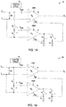
- FIGS. 1A and 1B are schematic diagrams of an example of auto-zero amplifier circuit.
- FIG. 1A depicts the example of an auto-zero amplifier circuit 10 in a first phase
- FIG. 1B depicts the example of the auto-zero amplifier circuit 10 in a second phase.
- the auto-zero amplifier 10 of FIGS. 1A and 1B can include a nulling amplifier circuit 12, a main amplifier circuit 14, ⁇ A switches that close in a first phase (Phase A) and open in a second phase (Phase B), and complementary ⁇ B switches that open in the first phase (Phase A), and close in the second phase (Phase B).
- a control circuit 16 can include an oscillator and can control operation of the ⁇ A switches and the ⁇ B switches.
- the nulling amplifier 12 has an offset voltage of V OSA and the main amplifier 14 has an offset voltage of V OSB .
- the amplifier circuit 10 can receive a differential input signal V I+ and V I- and generate an output signal V o .
- the amplifier circuit 10 can receive a differential input signal V I+ and V I- and generate a single-ended output signal V o , for example.
- V I+ and V I- Components in FIG. 2 that are similar to components in FIGS. 1A and 1B are labeled with similar reference numbers and, for purposes of conciseness, will not be described in detail again.
- the amplifier circuits in this disclosure can be implemented using CMOS operational amplifiers or bipolar operational amplifiers.
- the control circuit 22 can control the ⁇ A and ⁇ B switches to couple the auto-zero capacitor C3 to a first reference voltage VREF1 and decouple the auto-zero capacitor C4 from a second reference voltage VREF2.
- the auto-zero capacitor C3 can be charged to the first reference voltage VREF1.
- the auto-zero capacitor C3 can store the first reference voltage VREF1, e.g., like a "sample and hold" operation.
- the input offset voltage for the nulling amplifier 12 is stored on the auto-zero capacitor C1.
- the control circuit 22 can control the ⁇ A and ⁇ B switches to decouple the auto-zero capacitor C3 from the first reference voltage VREF1 and couple the auto-zero capacitor C4 to the second reference voltage VREF2.
- the input offset voltage of the auto-zero capacitor C1 is applied to the nulling input of the nulling amplifier 12.
- the first reference voltage VREF1 that was stored on the auto-zero capacitor C3 is applied to a reference voltage input of the nulling amplifier 12.
- the nulling amplifier 12 is configured to generate an amplifier circuit compensation signal using a difference between the input offset voltage (stored on the auto-zero capacitor C1) and the first reference voltage VREF1 (stored on the auto-zero capacitor C3).
- the nulling amplifier 12 can use the compensation signal to generate an error signal that can be injected into various nodes within the nulling amplifier circuitry to correct for the offset.
- the auto-zero capacitor C4 can be charged to the second reference voltage VREF2. In this manner, the auto-zero capacitor C4 can store the second reference voltage VREF2. As described above with respect to FIG. 1A , the input offset voltage for the main amplifier 14 is stored on the auto-zero capacitor C2.
- the additional capacitor C6 can leak current at a rate and in a manner similar to the auto-zero capacitor C5 to negate the effects of the leakage, e.g., due to the temperature variation, noise coupling, etc.
Landscapes
- Engineering & Computer Science (AREA)
- Power Engineering (AREA)
- Amplifiers (AREA)
Abstract
Description
- This document pertains generally, but not by way of limitation, to operational amplifiers and, more particularly, to auto-zero amplifiers.
- CMOS technology produces switches and capacitors with high performance and yield. CMOS operational amplifiers ("op amps"), however, can suffer from several drawbacks. More example, CMOS op amps typically have input offset voltages within the range of 1-10 millivolts (mV), whereas ideally the input offset voltage should be zero. During operation, the difference between the voltages on the input terminals of the op amp is equal to the input offset voltage when the output voltage is at zero volts. In addition, such op amps typically have a finite gain within the range of 100-1,000,000 (though ideally the gain should be infinite). As a result of the finite gain, there can exist an additional error voltage between the op amp input terminals that varies as the output voltage varies, which can cause inaccurate performance. Therefore, CMOS op amps can significantly adversely affect the accuracy of the circuit in which they are used.
- Using various techniques of this disclosure, an additional capacitor (or other capacitive component) can be added to an auto-zero circuit and can be switchably coupled to a reference voltage. Then, the auto-zero amplifier circuit can generate an auto-zero compensation signal using a difference between the reference voltage stored on the additional capacitor and a voltage stored on another auto-zero capacitor. Using an additional capacitor in the auto-zero circuit to store the reference voltage to generate the compensation signal can negate the effects of leakage due to temperature variation and/or noise coupling.
- In some aspects, this disclosure is directed to an auto-zero amplifier circuit to compensate for offset drift. The circuit comprises a first amplifier circuit having a first input offset voltage; a first auto-zero capacitor configured to be switchably coupled to the first amplifier circuit using a first switch, the first auto-zero capacitor configured to store the first input offset voltage; and a second auto-zero capacitor configured to be switchably coupled using a second switch to a first reference voltage to store the first reference voltage, wherein the first amplifier circuit is configured to generate a first amplifier circuit compensation signal using a difference between the first input offset voltage stored on the first auto-zero capacitor and the first reference voltage stored on the second auto-zero capacitor.
- In some aspects, this disclosure is directed to a method of compensating an auto-zero amplifier circuit for offset drift. The method comprises coupling, using a first switch, a first auto-zero capacitor to a first amplifier circuit to store a first input offset voltage of the first amplifier circuit; coupling, using a second switch, a second auto-zero capacitor to a first reference voltage to store the first reference voltage; and generating a first compensation signal using a difference between the first input offset voltage stored on the first auto-zero capacitor and the first reference voltage stored on the second auto-zero capacitor.
- In some aspects, this disclosure is directed to an auto-zero amplifier circuit to compensate for offset drift. The circuit comprises a first amplifier circuit having a first input offset voltage; means for storing a first input offset voltage of the first amplifier circuit; means for storing a first reference voltage, wherein the first amplifier circuit is configured to generate a first amplifier circuit compensation signal using a difference between the stored first input offset voltage and the stored first reference voltage.
- This overview is intended to provide an overview of subject matter of the present patent application. It is not intended to provide an exclusive or exhaustive explanation of the invention. The detailed description is included to provide further information about the present patent application.
- In the drawings, which are not necessarily drawn to scale, like numerals may describe similar components in different views. Like numerals having different letter suffixes may represent different instances of similar components. The drawings illustrate generally, by way of example, but not by way of limitation, various embodiments discussed in the present document.
-
FIGS. 1A and 1B are schematic diagrams of an example of auto-zero amplifier circuit. -
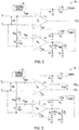
FIG. 2 is a schematic diagram of an example of an auto-zero amplifier circuit with improved immunity to offset drift. -
FIG. 3 is a schematic diagram of another example of an auto-zero amplifier circuit with improved immunity to offset drift. -
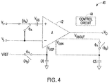
FIG. 4 is a schematic diagram of another example of an auto-zero amplifier circuit with improved immunity to offset drift. - To compensate for the non-ideal performance of CMOS or BJT operational amplifiers, auto-zeroing features can reduce offset voltage and gain errors. Due to various factors, such as temperature variation and/or noise coupling, the offset voltage of an operational amplifier can drift over time. The present inventors have recognized a need to be able to improve the immunity of the operational amplifier to offset drift due to temperature variation and noise coupling, for example.
- Using various techniques of this disclosure, an additional capacitor (or other capacitive component) can be added to an auto-zero circuit and can be switchably coupled to a reference voltage. Then, the auto-zero amplifier circuit can generate an auto-zero compensation signal using a difference between the reference voltage stored on the additional capacitor and a voltage stored on another auto-zero capacitor. The present inventors have recognized that by using an additional capacitor in the auto-zero circuit to store the reference voltage to generate the compensation signal, rather than using the reference voltage directly to generate the compensation signal, the additional capacitor can leak current at a rate and in a manner similar to the auto-zero capacitor, which can negate the effects of the leakage due to the temperature variation and/or noise coupling.
-
FIGS. 1A and 1B are schematic diagrams of an example of auto-zero amplifier circuit.FIG. 1A depicts the example of an auto-zero amplifier circuit 10 in a first phase andFIG. 1B depicts the example of the auto-zero amplifier circuit 10 in a second phase. The auto-zeroamplifier 10 ofFIGS. 1A and 1B can include anulling amplifier circuit 12, amain amplifier circuit 14, φA switches that close in a first phase (Phase A) and open in a second phase (Phase B), and complementary φB switches that open in the first phase (Phase A), and close in the second phase (Phase B). Acontrol circuit 16 can include an oscillator and can control operation of the φA switches and the φB switches. Thenulling amplifier 12 has an offset voltage of VOSA and themain amplifier 14 has an offset voltage of VOSB. Theamplifier circuit 10 can receive a differential input signal VI+ and VI- and generate an output signal Vo. - In the first (or nulling) phase (Phase A) shown in
FIG. 1A , the φA switches are closed (and the φB switches are opened) and the differential input signal VI+ and VI- is applied to themain amplifier 14. In the nulling phase, the inputs of thenulling amplifier 12 are shorted together and to the inverting input terminal (common mode input voltage) of thenulling amplifier 12. Thenulling amplifier 12 nulls its own offset voltage VOSA by feeding back to its nulling terminal whatever opposing voltage VNA is required to make the product of that voltage and the incremental gain of the nulling input approximately equal to the input offset voltage VOSA of thenulling amplifier 12. The nulling voltage is also stored on a first auto-zero capacitor C1. The auto-zero capacitor C1 is configured to store the input offset voltage VOSA and be switchably coupled to thenulling amplifier 12 using a φA switch. Meanwhile, themain amplifier 14 operates like a normal op amp. The nulling voltage of themain amplifier 14 is supplied by the voltage stored on a second auto-zero capacitor C2. The auto-zero capacitor C2 is configured to store the input offset voltage VOSB and be switchably coupled to themain amplifier 14 using a φB switch. - During the second (or output) phase (Phase B) shown in
FIG. 1B , the φB switches are closed (and the φA switches are opened) and the inputs of thenulling amplifier 12 are connected to the input terminals of themain amplifier 14, which couples the differential input signal VI+ and VI- to the inputs of thenulling amplifier 12. The auto-zero capacitor C1 continues to supply the nulling amplifier's required offset correction voltage. The differential input signal VI+ and VI- is amplified by thenulling amplifier 12 and is further amplified by the incremental gain of the main amplifier's nulling input circuitry. The differential input signal VI+ and VI- is also directly amplified by the gain of themain amplifier 14 itself. - The op amp feedback will cause the output voltage of the
nulling amplifier 12 to be whatever voltage VNB is necessary at the main amplifier's nulling input to bring the main amplifier's input difference voltage to near-null. The output of thenulling amplifier 12 is also stored on the second auto-zero capacitor C2, which can hold that required voltage during the next Phase A. In Phase B, with its nulling voltage furnished by the first auto-zero capacitor C1, thenulling amplifier 12 amplifies the differential input signal VI+ and VI- applied to themain amplifier 14 and applies the amplified voltage to the nulling input of the main amplifier and the capacitor C2. - To correct its offset voltage VOSA, the
nulling amplifier 12 can generate a nulling amplifier compensation signal using a difference between the voltage VNA applied at its nulling terminal and a reference voltage VREF. Similarly, to correct its offset voltage VOSB, themain amplifier 14 can generate a main amplifier compensation signal using a difference between the voltage VNB applied at its nulling terminal and a reference voltage VREF. - Due to various factors, such as temperature variation and/or noise coupling, the offset voltage of an operational amplifier can drift over time. For example, as the temperature increases, the auto-zero capacitor C1 can leak in phase B and the auto-zero capacitor C2 can leak in phase A, which can cause offset voltage drift. The present inventors have recognized a need to be able to improve the immunity of the operational amplifier to offset drift.
- As described below, the present inventors have recognized that by using one or more additional capacitors in the auto-zero circuit to store a reference voltage to generate the compensation signal, rather than using the reference voltage directly to generate the compensation signal, the additional capacitor can leak current at a rate and in a manner similar to the auto-zero capacitor, which can negate the effects of the leakage due to the temperature variation and/or noise coupling.
-
FIG. 2 is a schematic diagram of an example of an auto-zero amplifier circuit with improved immunity to offset drift. The auto-zeroamplifier 20 ofFIG. 2 can include anulling amplifier circuit 12, amain amplifier circuit 14, φA switches that close in a first phase (Phase A) and open in a second phase (Phase B), and φB switches that open in the first phase (Phase A), and close in the second phase (Phase B). Acontrol circuit 22 can include an oscillator and can control operation of the φA switches and the φB switches. Thenulling amplifier 12 has an offset voltage of VOSA and themain amplifier 14 has an offset voltage of VOSB. Theamplifier circuit 10 can receive a differential input signal VI+ and VI- and generate a single-ended output signal Vo, for example. Components inFIG. 2 that are similar to components inFIGS. 1A and 1B are labeled with similar reference numbers and, for purposes of conciseness, will not be described in detail again. The amplifier circuits in this disclosure can be implemented using CMOS operational amplifiers or bipolar operational amplifiers. - The
circuit 20 ofFIG. 2 further includes two additional auto-zero capacitors, namely capacitors C3 and C4. The operation of the switches coupled to auto-zero capacitors C1 and C3 can be complementary to the operation of the switches coupled to auto-zero capacitors C2 and C4. - During phase A, the
control circuit 22 can control the φA and φB switches to couple the auto-zero capacitor C3 to a first reference voltage VREF1 and decouple the auto-zero capacitor C4 from a second reference voltage VREF2. During phase A, the auto-zero capacitor C3 can be charged to the first reference voltage VREF1. In this manner, the auto-zero capacitor C3 can store the first reference voltage VREF1, e.g., like a "sample and hold" operation. As described above with respect toFIG. 1A , the input offset voltage for thenulling amplifier 12 is stored on the auto-zero capacitor C1. - During phase B, the
control circuit 22 can control the φA and φB switches to decouple the auto-zero capacitor C3 from the first reference voltage VREF1 and couple the auto-zero capacitor C4 to the second reference voltage VREF2. The input offset voltage of the auto-zero capacitor C1 is applied to the nulling input of thenulling amplifier 12. In addition, the first reference voltage VREF1 that was stored on the auto-zero capacitor C3 is applied to a reference voltage input of thenulling amplifier 12. Thenulling amplifier 12 is configured to generate an amplifier circuit compensation signal using a difference between the input offset voltage (stored on the auto-zero capacitor C1) and the first reference voltage VREF1 (stored on the auto-zero capacitor C3). Thenulling amplifier 12 can use the compensation signal to generate an error signal that can be injected into various nodes within the nulling amplifier circuitry to correct for the offset. - During phase B, the auto-zero capacitor C4 can be charged to the second reference voltage VREF2. In this manner, the auto-zero capacitor C4 can store the second reference voltage VREF2. As described above with respect to
FIG. 1A , the input offset voltage for themain amplifier 14 is stored on the auto-zero capacitor C2. - During the next phase A, the
control circuit 22 can control the φA and φB switches to couple the auto-zero capacitor C3 to the first reference voltage VREF1 and decouple the auto-zero capacitor C4 from the second reference voltage VREF2. The input offset voltage of the auto-zero capacitor C2 is applied to the nulling input of themain amplifier 14. In addition, the second reference voltage VREF2 that was stored on the auto-zero capacitor C4 can be applied to a reference voltage input of themain amplifier 14. Themain amplifier 14 is configured to generate another amplifier circuit compensation signal using a difference between the input offset voltage (stored on the auto-zero capacitor C2) and the second reference voltage VREF1 (stored on the auto-zero capacitor C4). Themain amplifier 14 can use the compensation signal to generate an error signal that can be injected into various nodes within the nulling amplifier circuitry to correct for the offset. - By storing the reference voltages on the additional capacitors C3, C4 and using those stored voltages to generate the compensation signal, rather than using the reference voltage directly to generate the compensation signal, the additional capacitors C3, C4 can leak current at a rate and in a manner similar to the auto-zero capacitors C1, C2 to negate the effects of the leakage, e.g., due to the temperature variation, noise coupling, etc. In some example implementations, the capacitance of the capacitor C3 can be substantially equal to the capacitance of the capacitor C1, and the capacitance of the capacitor C4 can be substantially equal to the capacitance of the capacitor C2.
- In some example configurations, the reference voltages VREF1 and VREF2 can be the same reference voltage. In other example configurations, the reference voltages VREF1 and VREF2 can be different reference voltages.
- In some examples implementations, the amplifier circuit can be a differential input and single-ended out configuration, such as shown in
FIG. 2 , where an output terminal is referenced to ground. The techniques of this disclosure are also applicable to a differential input and differential output configuration, such as shown inFIG. 3 . -
FIG. 3 is a schematic diagram of another example of an auto-zero amplifier circuit with improved immunity to offset drift. The auto-zeroamplifier circuit 30 ofFIG. 3 is a fully differential configuration. The auto-zeroamplifier circuit 30 includes two output terminals Vo+ and Vo-. Theamplifier circuit 30 can receive a differential input signal VI+ and VI- and generate an output signal VOUT between the two output terminals Vo+ and Vo-. - Although described above with respect to
FIG. 2 as including two amplifier circuits, e.g., thenulling amplifier 12 and themain amplifier 14, the techniques of this disclosure are not limited to such configurations. Rather, an auto-zero amplifier circuit having a single amplifier circuit can implement various techniques of this disclosure, as shown inFIG. 4 . -
FIG. 4 is a schematic diagram of another example of an auto-zero amplifier circuit with improved immunity to offset drift. The auto-zeroamplifier circuit 40 includes asingle amplifier circuit 42, and switches that close in a first phase (Phase A, φA) and open in a second phase (Phase B, φB). The auto-zeroamplifier circuit 40 can include two auto-zero capacitors C5 and C6. In some example implementations, the capacitance of the capacitor C6 can be substantially equal to the capacitance of the capacitor C5. - A
control circuit 44 can include an oscillator and can control operation of the switches. The auto-zeroamplifier circuit 40 can receive a differential input signal VI+ and VI- and generate an output signal VO in the differential input, singled-ended output configuration ofFIG. 4 . In some example implementations, theamplifier circuit 40 can be implemented in a differential input, differential output configuration, such as shown inFIG. 3 . - During phase A, the
amplifier 42 is in its nulling period and can generate an offset compensation voltage VOSOUT to compensate for the offset voltage Vos present at the input terminals. Thecontrol circuit 44 can control switches to close (φA position) and the auto-zeroamplifier circuit 40 can store the offset compensation voltage VOSOUT on the auto-zero capacitor C5. With the switches closed, the auto-zero capacitor C6 can be coupled to the reference voltage VREF. During phase A, the auto-zero capacitor C6 can be charged to the reference voltage VREF. In this manner, the auto-zero capacitor C6 can store the reference voltage VREF1, e.g., like a "sample and hold" operation. During phase A, the output signal VO is not valid. - During phase B, the
control circuit 44 can control the switches to open (φB position). With the switches open, the voltage on the auto-zero capacitor C5 can be applied to a first nulling terminal VOSN of the amplifier 24 and the voltage on the auto-zero capacitor C6 can be applied to a second nulling terminal VOSP of theamplifier 42. Then, theamplifier circuit 42 can generate an auto-zero compensation signal using a difference between the reference voltage stored on the auto-zero capacitor C6 and the offset compensation voltage VOSOUT stored on the auto-zero capacitor C5. The output signal Vo represents the signal amplified by the differential signal (VI+ minus VI-) with the offset of theamplifier circuit 42 compensated by the capacitors C5 and C6. - By storing the reference voltage on the additional capacitor C6 and using that stored voltage to generate the compensation signal, rather than using the reference voltage directly to generate the compensation signal, the additional capacitor C6 can leak current at a rate and in a manner similar to the auto-zero capacitor C5 to negate the effects of the leakage, e.g., due to the temperature variation, noise coupling, etc.
- Each of the non-limiting aspects or examples described herein may stand on its own or may be combined in various permutations or combinations with one or more of the other examples.
- The above detailed description includes references to the accompanying drawings, which form a part of the detailed description. The drawings show, by way of illustration, specific embodiments in which the invention may be practiced. These embodiments are also referred to herein as "examples." Such examples may include elements in addition to those shown or described. However, the present inventors also contemplate examples in which only those elements shown or described are provided. Moreover, the present inventors also contemplate examples using any combination or permutation of those elements shown or described (or one or more aspects thereof), either with respect to a particular example (or one or more aspects thereof), or with respect to other examples (or one or more aspects thereof) shown or described herein.
- In the event of inconsistent usages between this document and any documents so incorporated by reference, the usage in this document controls.
- In this document, the terms "a" or "an" are used, as is common in patent documents, to include one or more than one, independent of any other instances or usages of "at least one" or "one or more." In this document, the term "or" is used to refer to a nonexclusive or, such that "A or B" includes "A but not B," "B but not A," and "A and B," unless otherwise indicated. In this document, the terms "including" and "in which" are used as the plain-English equivalents of the respective terms "comprising" and "wherein." Also, in the following claims, the terms "including" and "comprising" are open-ended, that is, a system, device, article, composition, formulation, or process that includes elements in addition to those listed after such a term in a claim are still deemed to fall within the scope of that claim. Moreover, in the following claims, the terms "first," "second," and "third," etc. are used merely as labels, and are not intended to impose numerical requirements on their objects.
- Method examples described herein may be machine or computer-implemented at least in part. Some examples may include a computer-readable medium or machine-readable medium encoded with instructions operable to configure an electronic device to perform methods as described in the above examples. An implementation of such methods may include code, such as microcode, assembly language code, a higher-level language code, or the like. Such code may include computer readable instructions for performing various methods. The code may form portions of computer program products. Further, in an example, the code may be tangibly stored on one or more volatile, non-transitory, or nonvolatile tangible computer-readable media, such as during execution or at other times. Examples of these tangible computer-readable media may include, but are not limited to, hard disks, removable magnetic disks, removable optical disks (e.g., compact discs and digital video discs), magnetic cassettes, memory cards or sticks, random access memories (RAMs), read only memories (ROMs), and the like.
- The above description is intended to be illustrative, and not restrictive. For example, the above-described examples (or one or more aspects thereof) may be used in combination with each other. Other embodiments may be used, such as by one of ordinary skill in the art upon reviewing the above description. The Abstract is provided to comply with 37 C.F.R. §1.72(b), to allow the reader to quickly ascertain the nature of the technical disclosure. It is submitted with the understanding that it will not be used to interpret or limit the scope or meaning of the claims. Also, in the above Detailed Description, various features may be grouped together to streamline the disclosure. This should not be interpreted as intending that an unclaimed disclosed feature is essential to any claim. Rather, inventive subject matter may lie in less than all features of a particular disclosed embodiment. Thus, the following claims are hereby incorporated into the Detailed Description as examples or embodiments, with each claim standing on its own as a separate embodiment, and it is contemplated that such embodiments may be combined with each other in various combinations or permutations. The scope of the invention should be determined with reference to the appended claims, along with the full scope of equivalents to which such claims are entitled.
Claims (15)
- An auto-zero amplifier circuit to compensate for offset drift, the circuit comprising:a first amplifier circuit having a first input offset voltage;a first auto-zero capacitor configured to be switchably coupled to the first amplifier circuit using a first switch, the first auto-zero capacitor configured to store the first input offset voltage; anda second auto-zero capacitor configured to be switchably coupled using a second switch to a first reference voltage to store the first reference voltage,wherein the first amplifier circuit is configured to generate a first amplifier circuit compensation signal using a difference between the first input offset voltage stored on the first auto-zero capacitor and the first reference voltage stored on the second auto-zero capacitor.
- The auto-zero amplifier circuit of claim 1, wherein the first amplifier circuit is configured to receive a differential input signal and generate a single-ended output signal; and/or
wherein the first auto-zero capacitor and the second auto-zero capacitor have the same capacitance. - The auto-zero amplifier circuit of claim 1 or 2, further comprising:a second amplifier circuit having a second input offset voltage;a third auto-zero capacitor configured to be switchably coupled to the second amplifier circuit using a third switch, the third auto-zero capacitor configured to store the second input offset voltage; anda fourth auto-zero capacitor configured to be switchably coupled using a fourth switch to a second reference voltage to store the second reference voltage,wherein the second amplifier circuit is configured to generate a second compensation signal using a difference between the second input offset voltage stored on the third auto-zero capacitor and the second reference voltage stored on the fourth auto-zero capacitor.
- The auto-zero amplifier circuit of claim 3, wherein the first amplifier circuit is configured to receive a differential input signal and generate a single-ended output signal; and/or
wherein the first reference voltage is equal to the second reference voltage. - The auto-zero amplifier circuit of claim 3 or 4, wherein the first auto-zero capacitor and the second auto-zero capacitor have the same capacitance, and wherein the third auto-zero capacitor and the fourth auto-zero capacitor have the same capacitance.
- The auto-zero amplifier circuit of any one of claims 3 to 5, further comprising:
a control circuit including an oscillator and configured to control operation of the first, second, third, and fourth switches, wherein an operation of the first and second switches is complementary to an operation of the third and fourth switches. - The auto-zero amplifier circuit of any one of claims 1 to 6, further comprising:
a fifth switch configured to connect first and second inputs of the first amplifier circuit to generate the first offset voltage at an output of the first amplifier circuit. - A method of compensating an auto-zero amplifier circuit for offset drift, the method comprising:coupling, using a first switch, a first auto-zero capacitor to a first amplifier circuit to store a first input offset voltage of the first amplifier circuit;coupling, using a second switch, a second auto-zero capacitor to a first reference voltage to store the first reference voltage; andgenerating a first compensation signal using a difference between the first input offset voltage stored on the first auto-zero capacitor and the first reference voltage stored on the second auto-zero capacitor.
- The method of claim 8, further comprising:receiving a differential input signal and generating a single-ended output signal; orreceiving a differential input signal and generating a differential output signal.
- The method of claim 8 or 9, wherein the first auto-zero capacitor and the second auto-zero capacitor have the same capacitance.
- The method of any one of claims 8 to 10, further comprising:a second amplifier circuit having a second input offset voltage;coupling, using a third switch, a third auto-zero capacitor to a second amplifier circuit, the second auto-zero capacitor configured to store the second input offset voltage; andcoupling, using a fourth switch, a fourth auto-zero capacitor to a second reference voltage to store the second reference voltage,generating a second compensation signal using a difference between the second input offset voltage stored on the third auto-zero capacitor and the second reference voltage stored on the fourth auto-zero capacitor.
- The method of claim 11, further comprising:receiving a differential input signal and generating a single-ended output signal; orreceiving a differential input signal and generating a differential output signal.
- The method of claim 11 or 12, wherein the first reference voltage is equal to the second reference voltage; and/or
the method further comprising:
connecting, using a fifth switch, first and second inputs of the first amplifier circuit to generate the first offset voltage at an output of the first amplifier circuit. - An auto-zero amplifier circuit to compensate for offset drift, the circuit comprising:a first amplifier circuit having a first input offset voltage;means for storing a first input offset voltage of the first amplifier circuit;means for storing a first reference voltage,wherein the first amplifier circuit is configured to generate a first amplifier circuit compensation signal using a difference between the stored first input offset voltage and the stored first reference voltage.
- The auto-zero amplifier circuit of claim 14, further comprising:a second amplifier circuit having a second input offset voltage;means for storing the second input offset voltage; andmeans for storing a second reference voltage,wherein the second amplifier circuit is configured to generate a second compensation signal using a difference between the stored second input offset voltage and the stored second reference voltage.
Applications Claiming Priority (1)
| Application Number | Priority Date | Filing Date | Title |
|---|---|---|---|
| US16/361,579 US11012037B2 (en) | 2019-03-22 | 2019-03-22 | Techniques for controlling an auto-zero amplifier |
Publications (1)
| Publication Number | Publication Date |
|---|---|
| EP3713083A1 true EP3713083A1 (en) | 2020-09-23 |
Family
ID=69770702
Family Applications (1)
| Application Number | Title | Priority Date | Filing Date |
|---|---|---|---|
| EP20161067.2A Withdrawn EP3713083A1 (en) | 2019-03-22 | 2020-03-05 | Techniques for controlling an auto-zero amplifier |
Country Status (3)
| Country | Link |
|---|---|
| US (1) | US11012037B2 (en) |
| EP (1) | EP3713083A1 (en) |
| CN (1) | CN111726087A (en) |
Cited By (1)
| Publication number | Priority date | Publication date | Assignee | Title |
|---|---|---|---|---|
| US11012037B2 (en) | 2019-03-22 | 2021-05-18 | Analog Devices International Unlimited Company | Techniques for controlling an auto-zero amplifier |
Families Citing this family (1)
| Publication number | Priority date | Publication date | Assignee | Title |
|---|---|---|---|---|
| TWI885667B (en) * | 2022-12-30 | 2025-06-01 | 新加坡商光寶科技新加坡私人有限公司 | Offset voltage compensation circuit and isolation amplifier device including the same |
Citations (3)
| Publication number | Priority date | Publication date | Assignee | Title |
|---|---|---|---|---|
| US20070013439A1 (en) * | 2005-05-04 | 2007-01-18 | Infineon Technologies Ag | Circuit arrangement having an amplifier arrangement and an offset compensation arrangement |
| US20080079413A1 (en) * | 2006-10-03 | 2008-04-03 | Ashburn Michael A | Auto-nulled bandgap reference system and strobed bandgap reference circuit |
| WO2012146714A2 (en) * | 2011-04-28 | 2012-11-01 | Zentrum Mikroelektronik Dresden Ag | Arrangement and method for producing an output voltage |
Family Cites Families (22)
| Publication number | Priority date | Publication date | Assignee | Title |
|---|---|---|---|---|
| US4190805A (en) * | 1977-12-19 | 1980-02-26 | Intersil, Inc. | Commutating autozero amplifier |
| US4345477A (en) | 1980-12-03 | 1982-08-24 | Honeywell Inc. | Semiconduction stress sensing apparatus |
| US4808942A (en) * | 1988-04-04 | 1989-02-28 | General Electric Company | Continuous mode auto-zero offset amplifier or integrator |
| JPH04501779A (en) | 1988-09-09 | 1992-03-26 | アナログ・ディバイセス・インコーポレーテッド | Sample and hold amplifier circuit |
| DE59007921D1 (en) | 1989-09-20 | 1995-01-19 | Itt Ind Gmbh Deutsche | Offset voltage balancing operational amplifier. |
| US5258664A (en) | 1991-07-05 | 1993-11-02 | Silicon Systems, Inc. | Operational amplifier with self contained sample and hold and auto zero |
| US5497123A (en) | 1994-12-23 | 1996-03-05 | Motorola, Inc. | Amplifier circuit having high linearity for cancelling third order harmonic distortion |
| US5663680A (en) | 1996-04-04 | 1997-09-02 | Nordeng; Arnold E. | Chopper stabilized amplifier having an additional differential amplifier stage for improved noise reduction |
| US6271784B1 (en) | 1997-08-12 | 2001-08-07 | Analog Devices, Inc. | Capacitor-based digital-to-analog converter with continuous time output |
| US6087897A (en) * | 1999-05-06 | 2000-07-11 | Burr-Brown Corporation | Offset and non-linearity compensated amplifier and method |
| US6653895B1 (en) | 2002-06-12 | 2003-11-25 | Texas Instruments Incorporated | Gain-boost nulling amplifier for auto-zero circuit |
| US7321260B2 (en) | 2006-03-07 | 2008-01-22 | Honeywell International, Inc. | Ping-pong auto-zero amplifier with glitch reduction |
| US7382183B2 (en) | 2006-07-18 | 2008-06-03 | Microchip Technology Incorporated | Minimizing switching noise and its effects in auto-zeroed amplifiers |
| US20080042742A1 (en) | 2006-08-15 | 2008-02-21 | Technoconcepts, Inc. | Distortion Nulling for Single-Ended High Dynamic Range RF Amplifier |
| JP2009017249A (en) | 2007-07-05 | 2009-01-22 | Hitachi Ltd | Amplifier circuit |
| US7636013B2 (en) * | 2007-07-25 | 2009-12-22 | Infineon Technologies Ag | Method and integrated circuit including an amplifier calibration circuit |
| US8698556B2 (en) | 2011-03-30 | 2014-04-15 | Microchip Technology Incorporated | Low switching error, small capacitors, auto-zero offset buffer amplifier |
| US8493139B2 (en) | 2011-11-17 | 2013-07-23 | Analog Devices, Inc. | Low noise auto-zero circuits for amplifiers |
| EP2779444B1 (en) | 2013-03-13 | 2017-12-27 | Linear Technology Corporation | Leakage Compensation For Switched Capacitor Integrators |
| US9444414B2 (en) | 2014-07-11 | 2016-09-13 | Qualcomm Incorporated | Current sense circuit using a single opamp having DC offset auto-zeroing |
| US11012037B2 (en) | 2019-03-22 | 2021-05-18 | Analog Devices International Unlimited Company | Techniques for controlling an auto-zero amplifier |
| US10833639B2 (en) | 2019-04-12 | 2020-11-10 | Analog Devices International Unlimited Company | Method for aliasing reduction in auto zero amplifier |
-
2019
- 2019-03-22 US US16/361,579 patent/US11012037B2/en active Active
-
2020
- 2020-03-05 EP EP20161067.2A patent/EP3713083A1/en not_active Withdrawn
- 2020-03-06 CN CN202010152133.6A patent/CN111726087A/en active Pending
Patent Citations (3)
| Publication number | Priority date | Publication date | Assignee | Title |
|---|---|---|---|---|
| US20070013439A1 (en) * | 2005-05-04 | 2007-01-18 | Infineon Technologies Ag | Circuit arrangement having an amplifier arrangement and an offset compensation arrangement |
| US20080079413A1 (en) * | 2006-10-03 | 2008-04-03 | Ashburn Michael A | Auto-nulled bandgap reference system and strobed bandgap reference circuit |
| WO2012146714A2 (en) * | 2011-04-28 | 2012-11-01 | Zentrum Mikroelektronik Dresden Ag | Arrangement and method for producing an output voltage |
Non-Patent Citations (4)
| Title |
|---|
| ANALOG DEVICES: "Zero-Drift, Single-Supply, Rail-to-Rail Input/Output Operational Amplifiers", 28 September 2015 (2015-09-28), pages 1 - 28, XP093076738, Retrieved from the Internet <URL:https://www.analog.com/media/en/technical-documentation/data-sheets/AD8571_8572_8574.pdf> [retrieved on 20230828] * |
| ENZ C C ET AL: "CIRCUIT TECHNIQUES FOR REDUCING THE EFFECTS OF OP-AMP IMPERFECTIONS: AUTOZEROING, CORRELATED DOUBLES SAMPLING, AND CHOPPER STABILIZATION", PROCEEDINGS OF THE IEEE, IEEE. NEW YORK, US, vol. 84, no. 11, 1 November 1996 (1996-11-01), pages 1584 - 1614, XP001122266, ISSN: 0018-9219, DOI: 10.1109/5.542410 * |
| FINVERS I G ET AL: "A HIGH TEMPERATURE PRECISION AMPLIFIER", IEEE JOURNAL OF SOLID-STATE CIRCUITS, IEEE, USA, vol. 30, no. 2, 1 February 1995 (1995-02-01), pages 120 - 128, XP000496302, ISSN: 0018-9200, DOI: 10.1109/4.341738 * |
| THOMAS KUGELSTADT: "Auto-zero amplifiers ease the design of high-precision circuits", ANALOG APPLICATIONS JOURNAL, 1 April 2005 (2005-04-01), pages 19 - 27, XP055379985, Retrieved from the Internet <URL:http://www.tij.co.jp/jp/lit/an/slyt204/slyt204.pdf> [retrieved on 20170609] * |
Cited By (1)
| Publication number | Priority date | Publication date | Assignee | Title |
|---|---|---|---|---|
| US11012037B2 (en) | 2019-03-22 | 2021-05-18 | Analog Devices International Unlimited Company | Techniques for controlling an auto-zero amplifier |
Also Published As
| Publication number | Publication date |
|---|---|
| US20200304078A1 (en) | 2020-09-24 |
| CN111726087A (en) | 2020-09-29 |
| US11012037B2 (en) | 2021-05-18 |
Similar Documents
| Publication | Publication Date | Title |
|---|---|---|
| US7696817B1 (en) | Auto-gain correction and common mode voltage cancellation in a precision amplifier | |
| CN108288955B (en) | Operational amplifier | |
| US9621145B2 (en) | Sense amplifier latch with offset correction | |
| EP1471646B1 (en) | Comparing circuit and offset compensating apparatus | |
| US7385426B1 (en) | Low current offset integrator with signal independent low input capacitance buffer circuit | |
| JP2017076942A (en) | Chopper stabilization amplifier | |
| US20140218115A1 (en) | Current compensation circuit, method and operational amplifier | |
| JPS6355108B2 (en) | ||
| CA1163331A (en) | Switched capacitor comparator | |
| US11012037B2 (en) | Techniques for controlling an auto-zero amplifier | |
| US20180284159A1 (en) | Current measurement techniques to compensate for shunt drift | |
| CN111917384B (en) | Amplifier Nonlinear Offset Drift Correction | |
| US7321260B2 (en) | Ping-pong auto-zero amplifier with glitch reduction | |
| JPH02141010A (en) | Precision operational amplifier | |
| US7504882B2 (en) | Differential amplifier circuit and semiconductor device | |
| US6844775B2 (en) | Operational amplifier with adjustable input offset | |
| US8115539B2 (en) | Operational amplifier | |
| CN102187575B (en) | Low-voltage self-calibrated cmos peak detector | |
| US7724081B2 (en) | Amplifier front-end with low-noise level shift | |
| JP6257019B2 (en) | Magnetic sensor | |
| US8653829B2 (en) | Method and system for high gain auto-zeroing arrangement for electronic circuits | |
| US9112523B1 (en) | Multiplying digital to analog converter (MDAC) with error compensation and method of operation | |
| US12381526B2 (en) | Amplifier circuit and sensor circuit | |
| JPS5851612A (en) | Comparison circuit | |
| US9461628B2 (en) | Single ended charge to voltage front-end circuit |
Legal Events
| Date | Code | Title | Description |
|---|---|---|---|
| PUAI | Public reference made under article 153(3) epc to a published international application that has entered the european phase |
Free format text: ORIGINAL CODE: 0009012 |
|
| STAA | Information on the status of an ep patent application or granted ep patent |
Free format text: STATUS: THE APPLICATION HAS BEEN PUBLISHED |
|
| AK | Designated contracting states |
Kind code of ref document: A1 Designated state(s): AL AT BE BG CH CY CZ DE DK EE ES FI FR GB GR HR HU IE IS IT LI LT LU LV MC MK MT NL NO PL PT RO RS SE SI SK SM TR |
|
| AX | Request for extension of the european patent |
Extension state: BA ME |
|
| STAA | Information on the status of an ep patent application or granted ep patent |
Free format text: STATUS: REQUEST FOR EXAMINATION WAS MADE |
|
| 17P | Request for examination filed |
Effective date: 20210322 |
|
| RBV | Designated contracting states (corrected) |
Designated state(s): AL AT BE BG CH CY CZ DE DK EE ES FI FR GB GR HR HU IE IS IT LI LT LU LV MC MK MT NL NO PL PT RO RS SE SI SK SM TR |
|
| STAA | Information on the status of an ep patent application or granted ep patent |
Free format text: STATUS: EXAMINATION IS IN PROGRESS |
|
| 17Q | First examination report despatched |
Effective date: 20220225 |
|
| STAA | Information on the status of an ep patent application or granted ep patent |
Free format text: STATUS: THE APPLICATION HAS BEEN WITHDRAWN |
|
| 18W | Application withdrawn |
Effective date: 20231207 |