EP3713082A1 - Amplification circuit - Google Patents
Amplification circuit Download PDFInfo
- Publication number
- EP3713082A1 EP3713082A1 EP20164523.1A EP20164523A EP3713082A1 EP 3713082 A1 EP3713082 A1 EP 3713082A1 EP 20164523 A EP20164523 A EP 20164523A EP 3713082 A1 EP3713082 A1 EP 3713082A1
- Authority
- EP
- European Patent Office
- Prior art keywords
- current
- transistor
- circuit
- collector
- transistors
- Prior art date
- Legal status (The legal status is an assumption and is not a legal conclusion. Google has not performed a legal analysis and makes no representation as to the accuracy of the status listed.)
- Granted
Links
Images

Classifications
-
- H—ELECTRICITY
- H03—ELECTRONIC CIRCUITRY
- H03F—AMPLIFIERS
- H03F3/00—Amplifiers with only discharge tubes or only semiconductor devices as amplifying elements
- H03F3/45—Differential amplifiers
- H03F3/45071—Differential amplifiers with semiconductor devices only
- H03F3/45076—Differential amplifiers with semiconductor devices only characterised by the way of implementation of the active amplifying circuit in the differential amplifier
- H03F3/45475—Differential amplifiers with semiconductor devices only characterised by the way of implementation of the active amplifying circuit in the differential amplifier using IC blocks as the active amplifying circuit
-
- H—ELECTRICITY
- H03—ELECTRONIC CIRCUITRY
- H03F—AMPLIFIERS
- H03F1/00—Details of amplifiers with only discharge tubes, only semiconductor devices or only unspecified devices as amplifying elements
- H03F1/02—Modifications of amplifiers to raise the efficiency, e.g. gliding Class A stages, use of an auxiliary oscillation
- H03F1/0205—Modifications of amplifiers to raise the efficiency, e.g. gliding Class A stages, use of an auxiliary oscillation in transistor amplifiers
-
- H—ELECTRICITY
- H03—ELECTRONIC CIRCUITRY
- H03F—AMPLIFIERS
- H03F1/00—Details of amplifiers with only discharge tubes, only semiconductor devices or only unspecified devices as amplifying elements
- H03F1/30—Modifications of amplifiers to reduce influence of variations of temperature or supply voltage or other physical parameters
- H03F1/307—Modifications of amplifiers to reduce influence of variations of temperature or supply voltage or other physical parameters in push-pull amplifiers
-
- H—ELECTRICITY
- H03—ELECTRONIC CIRCUITRY
- H03F—AMPLIFIERS
- H03F1/00—Details of amplifiers with only discharge tubes, only semiconductor devices or only unspecified devices as amplifying elements
- H03F1/32—Modifications of amplifiers to reduce non-linear distortion
- H03F1/3211—Modifications of amplifiers to reduce non-linear distortion in differential amplifiers
-
- H—ELECTRICITY
- H03—ELECTRONIC CIRCUITRY
- H03F—AMPLIFIERS
- H03F1/00—Details of amplifiers with only discharge tubes, only semiconductor devices or only unspecified devices as amplifying elements
- H03F1/32—Modifications of amplifiers to reduce non-linear distortion
- H03F1/3217—Modifications of amplifiers to reduce non-linear distortion in single ended push-pull amplifiers
-
- H—ELECTRICITY
- H03—ELECTRONIC CIRCUITRY
- H03F—AMPLIFIERS
- H03F3/00—Amplifiers with only discharge tubes or only semiconductor devices as amplifying elements
- H03F3/181—Low-frequency amplifiers, e.g. audio preamplifiers
- H03F3/183—Low-frequency amplifiers, e.g. audio preamplifiers with semiconductor devices only
-
- H—ELECTRICITY
- H03—ELECTRONIC CIRCUITRY
- H03F—AMPLIFIERS
- H03F3/00—Amplifiers with only discharge tubes or only semiconductor devices as amplifying elements
- H03F3/181—Low-frequency amplifiers, e.g. audio preamplifiers
- H03F3/183—Low-frequency amplifiers, e.g. audio preamplifiers with semiconductor devices only
- H03F3/185—Low-frequency amplifiers, e.g. audio preamplifiers with semiconductor devices only with field-effect devices
- H03F3/1855—Low-frequency amplifiers, e.g. audio preamplifiers with semiconductor devices only with field-effect devices with junction-FET devices
-
- H—ELECTRICITY
- H03—ELECTRONIC CIRCUITRY
- H03F—AMPLIFIERS
- H03F3/00—Amplifiers with only discharge tubes or only semiconductor devices as amplifying elements
- H03F3/26—Push-pull amplifiers; Phase-splitters therefor
-
- H—ELECTRICITY
- H03—ELECTRONIC CIRCUITRY
- H03F—AMPLIFIERS
- H03F3/00—Amplifiers with only discharge tubes or only semiconductor devices as amplifying elements
- H03F3/30—Single-ended push-pull [SEPP] amplifiers; Phase-splitters therefor
- H03F3/3081—Duplicated single-ended push-pull arrangements, i.e. bridge circuits
-
- H—ELECTRICITY
- H03—ELECTRONIC CIRCUITRY
- H03F—AMPLIFIERS
- H03F3/00—Amplifiers with only discharge tubes or only semiconductor devices as amplifying elements
- H03F3/34—DC amplifiers in which all stages are DC-coupled
- H03F3/343—DC amplifiers in which all stages are DC-coupled with semiconductor devices only
- H03F3/3432—DC amplifiers in which all stages are DC-coupled with semiconductor devices only with bipolar transistors
- H03F3/3435—DC amplifiers in which all stages are DC-coupled with semiconductor devices only with bipolar transistors using Darlington amplifiers
-
- H—ELECTRICITY
- H03—ELECTRONIC CIRCUITRY
- H03F—AMPLIFIERS
- H03F3/00—Amplifiers with only discharge tubes or only semiconductor devices as amplifying elements
- H03F3/45—Differential amplifiers
- H03F3/45071—Differential amplifiers with semiconductor devices only
- H03F3/45076—Differential amplifiers with semiconductor devices only characterised by the way of implementation of the active amplifying circuit in the differential amplifier
- H03F3/4508—Differential amplifiers with semiconductor devices only characterised by the way of implementation of the active amplifying circuit in the differential amplifier using bipolar transistors as the active amplifying circuit
- H03F3/45174—Mirror types
-
- H—ELECTRICITY
- H03—ELECTRONIC CIRCUITRY
- H03F—AMPLIFIERS
- H03F3/00—Amplifiers with only discharge tubes or only semiconductor devices as amplifying elements
- H03F3/45—Differential amplifiers
- H03F3/45071—Differential amplifiers with semiconductor devices only
- H03F3/45076—Differential amplifiers with semiconductor devices only characterised by the way of implementation of the active amplifying circuit in the differential amplifier
- H03F3/45278—Differential amplifiers with semiconductor devices only characterised by the way of implementation of the active amplifying circuit in the differential amplifier using BiFET transistors as the active amplifying circuit
- H03F3/45282—Long tailed pairs
-
- H—ELECTRICITY
- H03—ELECTRONIC CIRCUITRY
- H03F—AMPLIFIERS
- H03F3/00—Amplifiers with only discharge tubes or only semiconductor devices as amplifying elements
- H03F3/45—Differential amplifiers
- H03F3/45071—Differential amplifiers with semiconductor devices only
- H03F3/45076—Differential amplifiers with semiconductor devices only characterised by the way of implementation of the active amplifying circuit in the differential amplifier
- H03F3/45278—Differential amplifiers with semiconductor devices only characterised by the way of implementation of the active amplifying circuit in the differential amplifier using BiFET transistors as the active amplifying circuit
- H03F3/45372—Mirror types
-
- H—ELECTRICITY
- H03—ELECTRONIC CIRCUITRY
- H03F—AMPLIFIERS
- H03F2200/00—Indexing scheme relating to amplifiers
- H03F2200/03—Indexing scheme relating to amplifiers the amplifier being designed for audio applications
-
- H—ELECTRICITY
- H03—ELECTRONIC CIRCUITRY
- H03F—AMPLIFIERS
- H03F2200/00—Indexing scheme relating to amplifiers
- H03F2200/91—Indexing scheme relating to amplifiers the amplifier has a current mode topology
-
- H—ELECTRICITY
- H03—ELECTRONIC CIRCUITRY
- H03F—AMPLIFIERS
- H03F2200/00—Indexing scheme relating to amplifiers
- H03F2200/93—Two or more transistors are coupled in a Darlington composite transistor configuration, all transistors being of the same type
-
- H—ELECTRICITY
- H03—ELECTRONIC CIRCUITRY
- H03F—AMPLIFIERS
- H03F2200/00—Indexing scheme relating to amplifiers
- H03F2200/96—Two or more complementary transistors are coupled in a Darlington composite transistor configuration
-
- H—ELECTRICITY
- H03—ELECTRONIC CIRCUITRY
- H03F—AMPLIFIERS
- H03F2203/00—Indexing scheme relating to amplifiers with only discharge tubes or only semiconductor devices as amplifying elements covered by H03F3/00
- H03F2203/45—Indexing scheme relating to differential amplifiers
- H03F2203/45134—Indexing scheme relating to differential amplifiers the whole differential amplifier together with other coupled stages being fully differential realised
Definitions
- the present invention relates to an amplification circuit using a current-current conversion circuit.
- the current-current conversion circuit has four transistors that constitute a translinear circuit by using their PN junctions, and constant current sources.
- the current-current conversion circuit has two complementary pairs in each of which transistors are in the complementary configuration, i.e., an NPN transistor on the higher potential side and a PNP transistor on the lower potential side are connected in series.
- the base of the NPN transistor of the first complementary pair and that of the NPN transistor of the second complementary pair are commonly connected to the collector of the NPN transistor of the second complementary pair.
- the emitter of the NPN transistor of the first complementary pair is connected to that of the PNP transistor of the same complementary pair, and the emitter of the NPN transistor of the second complementary pair is connected to that of the PNP transistor of the same complementary pair.
- the base of the PNP transistor of the first complementary pair and that of the PNP transistor of the second complementary pair are connected to the collector of the PNP transistor of the second complementary pair.
- the constant current sources are connected in series to the second complementary pair.
- the common connection node of the emitters of the NPN transistor and the PNP transistor is set as an input node.
- the amplification circuit of JP-A-H8-32367 is configured basically in a similar manner.
- the collector currents of the NPN transistor and the PNP transistor of the first complementary pair are controlled so that the input current to the input node is equal to the difference between the collector currents, and the product of the collector currents has a constant value.
- the collector current of a transistor between the output terminal of the output stage of the amplification circuit and the positive power supply is proportional to the collector current of the NPN transistor of the first complementary pair of the current-current conversion circuit.
- the collector current of a transistor between the output terminal and the negative power supply is proportional to the collector current of the PNP transistor of the first complementary pair of the current-current conversion circuit. Then, the collector currents of the two transistors of the output stage are combined with each other to drive the load.
- the collector current of each of the PNP transistors in a region where the input current is positive, in accordance with a positive direction change of the input current, the collector current of each of the PNP transistors is increased, and, on the other hand, that of each of the NPN transistors is decreased. In a region where the input current is negative, in accordance with a negative direction change of the input current, the collector current of the NPN transistor is increased, and, on the other hand, that of the PNP transistor is decreased.
- the product of the collector currents of the NPN transistor and the PNP transistor is always constant.
- the collector current of the NPN transistor is decreased in accordance with a positive direction change of the input current, but the collector current of the NPN transistor does not become zero.
- the collector current of the PNP transistor is decreased in accordance with a negative direction change of the input current, but the collector current of the PNP transistor does not become zero.
- the amplification circuit In the current-current conversion circuit, the difference between the collector currents of the NPN transistor and PNP transistor, and the input current are linearly related that the relationship line passes through the origin. A current that is proportional to the difference flows from the output stage of the amplification circuit to the load. Therefore, the amplification circuit can realize high linearity.
- a totem-pole output stage an output stage in which same-polarity elements are connected in a totem-pole configuration
- MOSFETs Metal Oxide Semiconductor Field Effect Transistors
- the positive and negative inputs are configured by a pair of inputs of the current sink and source types.
- a totem-pole output stage when one input is of the current sink type, by contrast, also the other input is of the current sink type, and, when one input is of the current source type, also the other input is of the current source type.
- the invention has been conducted in view of the above-discussed circumstances. It is an object of the invention to provide an amplification circuit including a current-current conversion circuit which is excellent in linearity, in which the idle current is low, and which is suitable for an output stage configured by transistors of the same polarity.
- the invention provides an amplification circuit including: a current-current conversion circuit having: a first transistor; a second transistor that has a same polarity as the first transistor, a collector and a base of the second transistor being connected to a base of the first transistor; a third transistor that has the same polarity as the first transistor, a collector and a base of the third transistor being connected to an emitter of the first transistor; a fourth transistor that has the same polarity as the first transistor, a collector and a base of the fourth transistor being connected to an emitter of the second transistor; and a constant current source that is connected in series to the second transistor and the fourth transistor, an input signal being applied to a connection node of the first transistor and the third transistor; and a current generation circuit including: a first current generating section that supplies a first current to a load based on a collector current of the first transistor; and a second current generating section that supplies a second current to the load based on the collector current of the third transistor.
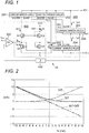
- Fig. 1 is a circuit diagram showing the configuration of an amplification circuit 1A of a first embodiment of the invention.
- the amplification circuit 1A includes a current-current conversion circuit 100, a current generation circuit 200, a transconductance amplifier 300, and a feedback circuit 400.
- the current-current conversion circuit 100 has a first transistor Q1, a second transistor Q2, a third transistor Q3, a fourth transistor Q4, and a constant current source 101 of a current value Id.
- the transistors Q1 to Q4 are transistors having the same characteristics and polarities. Specifically, all of the transistors Q1 to Q4 are NPN transistors.
- the transistor Q2 is diode-connected, i.e., the collector and the base are connected to each other.
- the transistor Q3 is diode-connected, and connected in series to the transistor Q1.
- the collector and the base are connected to the emitter of the transistor Q1, and the emitter is grounded.
- the transistor Q4 is diode-connected, and connected in series to the transistor Q2.
- the collector and the base are connected to the emitter of the transistor Q2, and the emitter is grounded.
- the constant current source 101 is connected in series to the transistors Q2 and Q4. Specifically, the constant current source 101 is connected between the collector of the transistor Q2 and a positive power supply V(+).
- transistors Q1 and Q2 their bases are connected to each other. Therefore, a control voltage that is common to the transistors Q1 and Q2 is applied to the transistor Q1. Both the emitters of the transistors Q3 and Q4 are grounded, and therefore the transistors Q1, Q2, Q3, and Q4 constitute a translinear circuit that forms a single loop by using only the PN junctions of the transistors. An input signal current Ix is given to the common connection node of the transistors Q1 and Q3.
- the current generation circuit 200 includes current mirror circuits 201 to 204 and a transistor Q5. Currents that are proportional respectively to the currents which are input to the master sides of the current mirror circuits 201 to 204 are output to the slave sides of the current mirror circuits.
- the transistors Q3 and Q5 their bases are connected to each other, and their emitters are connected to each other, thereby constituting a translinear circuit.
- the base current Ib3 of the transistor Q3 is sufficiently smaller than the collector current Ic3, and the base current Ib5 of the transistor Q5 is sufficiently smaller than the collector current Ic5 (even in a very usual element, about one hundredth or less). Therefore, the collector current Ic5 of the transistor Q5 becomes equal to the collector current Ic3 of the transistor Q3.
- the current mirror circuits 201 and 203 function as the first current generating section that supplies a first current to a load based on the collector current of the first transistor Q1, and the transistor Q5 and the current mirror circuits 202 and 204 function as the second current generating section that supplies a second current to the load based on the collector current of the third transistor Q3.
- the master side of the current mirror circuit 201 is connected to the collector of the transistor Q1, and the slave side is connected to the master side of the current mirror circuit 203. Therefore, a current that is proportional to the collector current Ic1 of the transistor Q1 is supplied to the master side of the current mirror circuit 203.
- the master side of the current mirror circuit 202 is connected to the collector of the transistor Q5, and the slave side is connected to the master side of the current mirror circuit 204. Therefore, a current that is proportional to the collector current Ic5 of the transistor Q5 is supplied to the master side of the current mirror circuit 204.
- the load such as a speaker is connected to an output terminal 208.
- the current mirror circuit 203 supplies a current that is proportional to the current supplied through the current mirror circuit 201, i.e., a current A ⁇ Ic1 that is proportional to the collector current of the transistor Q1, to the output terminal 208.
- the current mirror circuit 204 pulls in a current that is proportional to the current supplied through the current mirror circuit 202, i.e., a current A ⁇ Ic5 that is proportional to the collector current of the transistor Q5, from the output terminal 208.
- the current generation circuit 200 supplies a current corresponding to the difference between the first current A ⁇ Ic1 and the second current A ⁇ Ic5, to the load based on the collector current of the first transistor Q1, and the collector current of the third transistor Q3.
- the transconductance amplifier 300 supplies a current signal Ix that is proportional to the differential input voltage, as the input signal to the common connection node of the transistors Q1 and Q3, i.e., the input node of the current-current conversion circuit 100. Because of the feedback circuit 400, the output signal Vout that is generated at the output terminal 208 is negatively fed back at a feedback factor ⁇ to the transconductance amplifier 300, and therefore the amplification circuit 1A constitutes a non-inverting amplification circuit.
- the transistors Q1 to Q5 having the same characteristics are thermally coupled with one another, and operate so that the base-emitter junctions are forward biased.
- Ic 1 ⁇ Ix + ⁇ Ix 2 + 4 ⁇ Id 2 / 2
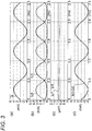
- Fig. 2 is a graph that shows the current Ic1 indicated in equation (10), the current Ic5 indicated in equation (14), and the value of Ic1 - Ic5 in the case where the input current Ix is changed.
- the current Id is 10 mA
- the input current Ix is changed from -10 mA to +10 mA.
- the other current only approaches zero, but never is cut off.
- the difference Ic1 - Ic5 between the currents Ic1 and Ic5 is expressed as a linear line that passes through the origin.
- the currents Ic1 and Ic5 are individually A (> 1) times current amplified by using the current mirror circuits 201 to 204, and the amplified currents are supplied to the output terminal 208.
- transistors (not shown) that are between the positive power supply (V+) in the current mirror circuit 203 and the output terminal 208, and transistors (not shown) that are between the negative power supply (V-) and the output terminal 208 are always in the active state. According to the embodiment, that is, it is possible to realize a same-polarity SEPP (Single Ended Push-Pull) amplifier in which the idle current is low, and which performs class-A operation.
- SEPP Single Ended Push-Pull
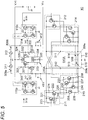
- FIG. 3 (a) to (d) show waveforms of the currents Ic1 and Ic5 (see (b)), the product (see (c)) of the currents Ic1 and Ic5, and the differential current Ic1 - Ic5 (see (d)) in the case where, in the embodiment, the current Id of the constant current source 101 is 1 mA, and a sinusoidal current of ⁇ 4 mA (see (a)) is input as the input signal Ix.
- the differential current Ic1 - Ic5 becomes a sinusoidal current of ⁇ 4 mA, and is strictly proportional to the input signal Ix.
- the first transistor Q1 and third transistor Q3 in the current-current conversion circuit 100 are transistors of the same polarity.
- the two current mirror circuits 201 and 203 and the other two current mirror circuits 202 and 204 constitute a circuit that is perfectly symmetrical. Therefore, a desired current can be supplied to the transistor that is in the output stage, and that is on the side of the positive power supply V(+), and the transistor that is in the output stage, and that is on the side of the negative power supply V(-), without causing the above-described problem.
- the current transmission path extending from the first transistor Q1 to the output terminal 208, and that extending from the third transistor Q3 to the output terminal 208 are not strictly symmetrical because the latter includes the fifth transistor Q5.
- the transistor Q5 constitutes together with the transistor Q3 the translinear circuit.
- the degree of the degradation of the characteristics of the amplification circuit A1 due to the disposition of the transistor Q5 is very smaller than that of the characteristics of the amplification circuit A1 that is caused by the asymmetry of the current mirror circuits.
- devices ranging from a line device that has a high load impedance (600 ⁇ to several tens of kQ), to a speaker that has a low load impedance (about several ohms) can be driven in class A with using a small amount of the idle current by the same amplification circuit 1A.
- Fig. 4 is a circuit diagram showing the configuration of an amplification circuit 1B of a second embodiment of the invention.
- balanced signal sources 311 and 312 that supply a positive phase input signal and a negative phase input signal to input terminals 309a and 309b of the amplification circuit 1B, and a load 518 such as a speaker are illustrated together with the amplification circuit 1B. Both ends of the speaker are connected to output terminals 209a and 209b of the amplification circuit 1B.
- the amplification circuit 1B has first and second current-current conversion circuits 110p and 110n that are configured in the same manner as the current-current conversion circuit 100 of the first embodiment, a current generation circuit 210, a differential transconductance amplifier 310, and an input circuit 315 that has input resistors 313 and 314 connected respectively to the input terminals 309a and 309b.
- the transconductance amplifier 310 differentially amplifies the positive phase input signal that is input from the signal source 311 through the resistor 313, and the negative phase input signal that is input from the signal source 312 through the resistor 314, whereby a positive phase input signal Ixp and negative phase input signal Ixn that are differential current signals are supplied to an input node of the current-current conversion circuit lOOp and that of the current-current conversion circuit 100n, respectively.
- the current generation circuit 210 has current mirror circuits 211 to 214. These circuits correspond to the current mirror circuits 201 to 204 in the first embodiment.
- the current mirror circuits 211 and 213 function as the first current generating section that supplies a first current between the first output terminal 209a and the second output terminal 209b through a first path including a first floating power supply 511, based on the collector current of the first transistor Q1 of the first current-current conversion circuit 110p.
- the current mirror circuits 212 and 214 function as the second current generating section that supplies a second current having the polarity opposite to the first current, between the first output terminal 209a and the second output terminal 209b through a second path including a second floating power supply 512, based on the collector current of the first transistor Q1 of the second current-current conversion circuit 110n.
- the master side of the current mirror circuit 211 is connected to the collector of the transistor Q1 of the current-current conversion circuit 110p, and the slave side is connected to the master side of the current mirror circuit 213. Therefore, a current that is proportional to the collector current Ic1p of the transistor Q1 of the current-current conversion circuit 110p is supplied to the master side of the current mirror circuit 213.
- the master side of the current mirror circuit 212 is connected to the collector of the transistor Q1 of the current-current conversion circuit 110n, and the slave side is connected to the master side of the current mirror circuit 214. Therefore, a current that is proportional to the collector current Ic1n of the transistor Q1 of the current-current conversion circuit 110n is supplied to the master side of the current mirror circuit 214.
- the slave side of the current mirror circuit 213, that of the current mirror circuit 214, the floating power supplies 511 and 512, and resistors 515 and 516 constitute an output stage circuit 510.
- the slave side of the current mirror circuit 213 is connected to the output terminal 209b.
- the slave side of the current mirror circuit 214 is connected to the output terminal 209a.
- the negative terminal is connected to the output terminal 209a, and the positive terminal is connected to the current mirror circuit 213.
- the floating power supply 512 the negative terminal is connected to the output terminal 209b, and the positive terminal is connected to the current mirror circuit 214.
- the current mirror circuit 213 supplies a first current A ⁇ Ic1p that is proportional to the collector current of the transistor Q1 of the current-current conversion circuit 110p, between the output terminals 209a and 209b through a first path including the floating power supply 511.
- the first path is a path flowing the output terminal 209a, the floating power supply 511, the current mirror circuit 213, and the output terminal 209b in this order.
- the current mirror circuit 214 supplies a second current A ⁇ Ic1n that is proportional to the collector current of the transistor Q1 of the current-current conversion circuit 110n, between the output terminals 209a and 209b through a second path including the floating power supply 512.
- the second path is a path flowing the output terminal 209b, the floating power supply 512, the current mirror circuit 214, and the output terminal 209a in this order.
- the second current is a current having the polarity opposite to the first current. Since the load 518 is connected between the output terminals 209a and 209b, two loops are formed.
- the first loop 513 is a loop including the floating power supply 511, the load 518, and the current mirror circuit 213.
- the second loop 514 is a loop including the floating power supply 512, the load 518, and the current mirror circuit 214.
- the first current A ⁇ Ic1p flows through the first loop 513
- the second current A ⁇ Ic1n flows through the second loop 514.
- One end of the resistor 515 is connected to the common connection node of the negative terminal of the floating power supply 511 and the current mirror circuit 213, and the other end is connected to the negative power supply V(-).
- On end of the resistor 516 is connected to the common connection node of the negative terminal of the floating power supply 512 and the current mirror circuit 214, and the other end is connected to the negative power supply V(-).
- resistors 515 and 516 are disposed.
- a balanced output amplification circuit must be driven so that the potentials of the both ends of a load with respect to the midpoint of the load are always kept symmetric.
- the negative terminals of the floating power supplies 511 and 512 are in a completely floating state, and therefore the potential of the midpoint of the load 518 is uncertain.
- the resistors 515 and 516 are disposed at the both ends of the load, and the potential of the common connection node of the resistors is fixed, thereby causing the potentials of the positive terminals of the floating power supplies 511 and 512 to change while always keeping the symmetry with respect to the potential of the midpoint of the load 518.
- each of the feedback circuits 411 and 412 may be configured by a resistor.
- the current A ⁇ Ic1p that is proportional to Ic1p of above equation (16) is supplied to the load 518 through the first loop 513, and the current A ⁇ Ic1n that is proportional to Ic1n of above equation (17) is supplied to the load 518 through the second loop 514.
- the transistors of the output stage i.e., the transistor that is inserted into the slave side of the current mirror circuit 213, and the transistor that is inserted into the slave side of the current mirror circuit 214 are not cut off, and the amplification circuit 1B operates as a class-A amplification circuit.
- the relationship between the differential current Ic1p - Ic1n, and the input positive phase signal Ixp or Ixn is indicated by a linear line that passes through the origin. Then, the current A ⁇ Ic1p that is proportional to the current Ic1p is flown to the load 518, and the current A ⁇ Ic1n that is proportional to the current Icln, and that is opposite in polarity to the current A ⁇ Ic1p is flown to the load 518. Therefore, a current A ⁇ (Ic1p - Ic1n) that is proportional to the differential current Ic1p - Ic1n is flown to the load 518. According to the embodiment, consequently, it is possible to realize a same-polarity balanced amplifier having high linearity.
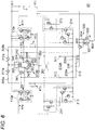
- Fig. 5 is a circuit diagram showing the configuration of an amplification circuit 1C that is a first specific example of the amplification circuit 1B.
- Fig. 5 portions that are common to the portions shown in Fig. 4 are denoted by the same reference numerals, and their description will be omitted.
- an output stage circuit 510A In an output stage circuit 510A, the positional relationship between the current mirror circuit 213 and floating power supply 511 in the first loop 513 is reversed to that in the output stage circuit 510, and the positional relationship between the current mirror circuit 214 and floating power supply 512 in the second loop 514 is reversed to that in the output stage circuit 510, whereby the load 518 is moved to a position between the negative terminals of the floating power supplies 511 and 512.
- the output stage circuit 510A is identical in function with the output stage circuit 510 of Fig. 4 .
- the current mirror circuit 211 a complementary current mirror circuit that includes a transistor 221 that is an NPN transistor, a transistor 222 that is a PNP transistor, and resistors 223 to 225 is employed.
- the resistor 223 is connected between the collector and the base, the collector is connected to the positive terminal of the floating power supply 512, and the base is connected to the collector of the transistors Q1 of the current-current conversion circuit 110p.
- the transistor 222 the emitter is connected to the positive terminal of the floating power supply 512 through the resistor 224, and the base is connected to the emitter of the transistors 221.
- One end of the resistor 225 is connected to the emitter of the transistor 221.
- the current mirror circuit 213 has transistors 231 to 233 that are NPN transistors, a transistor 234 that is a PNP transistor, and resistors 235 to 238.
- the collector is connected to the collector of the transistor 222, the base is connected to the emitter of the transistor 221 through the resistor 225, and the emitter is connected to the negative terminal of the floating power supply 512 through the resistor 236.
- the base is connected to a connection node of the collectors of the transistors 222 and 231 through the resistor 235, the collector is connected to the positive terminal of the floating power supply 511, and the emitter is connected to the negative terminal of the floating power supply 512 through the resistor 237.
- the base is connected to the emitter of the transistor 232, the collector is connected to the positive terminal of the floating power supply 511, and the emitter is connected to the negative terminal of the floating power supply 512 through the resistor 238.
- the base-emitter voltage of the transistor 221, and that of the transistor 222 are approximately equal to each other. Therefore, the current Ic1p that flows through the transistor Q1 of the current-current conversion circuit 110p flows through the resistor 223, and, when a voltage is generated across the resistor 223 by the current Ic1p, a voltage that is approximately equal to the generated voltage is generated across the resistor 224. Consequently, a current Ia that is obtained by multiplying the current Ic1p by a coefficient which is determined in accordance with the resistance ratio of the resistors 223 and 224 flows through the transistor 222.
- the base of the transistor 231 is connected to the transistor 221 through the resistor 225, and therefore the transistor 231 is turned ON.
- the current Ia that is output from the transistor 222 flows through the transistor 232 and 231 and the resistor 236.
- the transistors 231 and 234 constitute a feedback circuit, and their emitter-base voltages are approximately equal to each other.
- the current that is input to the transistor 232 from the current Ia is controlled so that the voltage that is generated across the resistor 236 by the flowing of the current Ia through the resistor 236, and the voltage that is generated across the resistor 238 by the flowing of the current through the resistor 238 are approximately equal to each other.
- a current that is proportional to the current Ia i.e., a current that is proportional to the current Ic1p is flown through the resistor 238 through the transistor 233.
- the current mirror circuit 213 pulls in the current A ⁇ Ic1p that is proportional to the current Ic1p which flows through the current-current conversion circuit 110p, form the floating power supply 511 in the first loop 513.
- the current mirror circuit 212 is configured in the same manner as the current mirror circuit 211, and the current mirror circuit 214 is configured in the same manner as the current mirror circuit 213.
- the current mirror circuits 212 and 214 are disposed between the positive and negative terminals of the floating power supply 511 in contrast that the current mirror circuits 211 and 213 are disposed between the positive and negative terminals of the floating power supply 512. Then, the current mirror circuit 214 pulls in the current A ⁇ Ic1n that is proportional to the current Ic1n which flows through the current-current conversion circuit 110n, form the floating power supply 512 in the second loop 514.
- Atransconductance amplifier 310A is a two-stage differential amplifier that has a first stage differential amplifier 320 and a second stage differential amplifier 330.
- the first stage differential amplifier 320 is configured by N-channel JFETs (Junction Field Effect Transistors) 321 and 322 and resistors 323 to 325.
- the second stage differential amplifier 330 is configured by transistors 331 and 332 that are PNP transistors, and resistors 333 to 335.
- the gate of the JFET 321 functions as the positive-phase input terminal of the transconductance amplifier 310A.
- the positive phase input signal is given from the signal source 311 to the positive-phase input terminal through the resistor 313.
- the gate of the JFET 322 functions as the negative-phase input terminal of the transconductance amplifier 310A.
- the negative phase input signal is given from the signal source 312 to the negative-phase input terminal through the resistor 314.
- the collector of the transistor 331 functions as the positive-phase output terminal of the transconductance amplifier 310A.
- the transconductance amplifier 310A supplies the positive phase input signal Ixp from the positive-phase output terminal to the current-current conversion circuit 110p.
- the collector of the transistor 332 functions as the negative-phase output terminal of the transconductance amplifier 310A.
- the transconductance amplifier 310A supplies the negative-phase input signal Ixn from the negative-phase output terminal to the current-current conversion circuit 110n.
- Fig. 6 is a circuit diagram showing the configuration of an amplification circuit 1D that is a second specific example of the amplification circuit 1B.
- portions that are common to the portions shown in Fig. 5 are denoted by the same reference numerals, and their description will be omitted.
- the signal sources 311 and 312 in Fig. 5 are replaced with signal sources 311a and 312a that are current sources, respectively, and the transconductance amplifier 310A in Fig. 5 is replaced with a transconductance amplifier 310B.
- resistors 361 and 362 and a potential controller 600 are added to the amplification circuit 1D.
- the signal sources 311a and 312a are current output DACs (Digital Analogue Converters) that convert a sampled value of, for example, a digital audio signal into a current value, and that output the current value.
- DACs Digital Analogue Converters
- the transconductance amplifier 310B is a two-stage differential amplifier that has a first stage differential amplifier 340 and a second stage differential amplifier 350.
- the first stage differential amplifier 340 is configured by P-channel JFETs 341 and 342 and resistors 343 to 345.
- the second stage differential amplifier 350 is configured by transistors 351 and 352 that are NPN transistors, and resistors 353 to 355.
- the gate of the JFET 341 functions as the positive-phase input terminal of the transconductance amplifier 310B.
- the positive phase input signal (current) is given from the signal source 311a to the positive-phase input terminal.
- the gate of the JFET 342 functions as the negative-phase input terminal of the transconductance amplifier 310B.
- the negative phase input signal (current) is given from the signal source 312a to the negative-phase input terminal.
- the collector of the transistor 351 functions as the positive-phase output terminal of the transconductance amplifier 310B.
- the transconductance amplifier 310B supplies the positive phase input signal Ixp from the positive-phase output terminal to the current-current conversion circuit 110p.
- the collector of the transistor 352 functions as the negative-phase output terminal of the transconductance amplifier 310B.
- the transconductance amplifier 310B supplies the negative-phase input signal Ixn from the negative-phase output terminal to the current-current conversion circuit 110n.
- the resistors 361 and 362 are connected in series between the gates of the JFETs 341 and 342.
- the neutral point potential between the gates of the JFETs 341 and 342 is obtained from the common connection node of the resistors 361 and 362.
- the potential controller 600 is a circuit for controlling the potential of the common connection node of the resistors 515 and 516.
- the reason why the potential controller 600 is disposed is as follows. In the circuit shown in Fig. 5 , the floating power supplies 511 and 512 of the output stage circuit 510A are floated, and therefore the current that is supplied, for example, from the grounded current-current conversion circuit 110p to the output stage circuit 510A flows back to the ground through the resistor 516. In the case where the load 518 having a low resistance is driven with large amplitude, therefore, the voltage corresponding to the current flowing through the resistor 516 appears in the output voltage for the load 518, and, in accordance with this, also the input potential of the transconductance amplifier 310A varies.
- the varying potential appears in phase at the positive and negative phase input terminals of the transconductance amplifier 310A, and therefore the differential signal that is output from the transconductance amplifier 310A is not affected.
- the current output DACs that function as the signal sources 311a and 312a are usually designed so as to supply a current to a virtual ground, and therefore it is not preferred from the viewpoint of operation that the input potential of the transconductance amplifier 310B is largely varied.
- the varying potential contains DC components of the currents that are supplied from the current-current conversion circuits 110p and 110n to the output stage circuit 510A, and equally appears at the positive side output that is one end of the load 518, and the negative side output that is the other end.
- a headphone or a speaker is operated by a differential output irrespective of the ground potential, and therefore does not suffer the problem of a DC component.
- a device is operated by the ground potential, and therefore there arises the problem of a DC component.
- the potential controller 600 is provided on the amplification circuit 1D shown in Fig. 6 .
- the potential controller 600 controls the midpoint between the positive and negative phase input terminals of the transconductance amplifier 310A so as to be always at the virtual ground.
- the potential controller 600 has N-channel JFETs 601 and 602, resistors 603 and 604, and a transistor 605 that is a PNP transistor.
- the emitter is connected to the positive power supply V(+), and the collector is connected to the common connection node of the resistors 515 and 516.
- the sources of the JFETs 601 and 602 are commonly connected to each other.
- the resistor 603 is connected between the common connection node and the negative power supply V(-).
- the drain of the JFET 601 is connected to the positive power supply V(+), and that of the JFET 602 is connected to the positive power supply V(+) through the resistor 604.
- the base of the transistor 605 is connected to the drain of the JFET 602.
- the gate of the JFET 602 is grounded, and that of the JFET 601 is connected to the common connection node of the resistors 361 and 362.
- the JFETs 601 and 602 and the resistors 603 and 604 constitute a differential amplifier.
- the potential of the common connection node of the resistors 361 and 362 is raised from the ground potential, the current flowing through the resistor 604 is decreased, and the potential of the common connection node of the resistors 515 and 516 is lowered. This causes the potential of the common connection node of the resistors 361 and 362 to be lowered.
- the potential of the common connection node of the resistors 361 and 362 is lowered from the ground potential, the current flowing through the resistor 604 is increased, and the potential of the common connection node of the resistors 515 and 516 is raised. This causes the potential of the common connection node of the resistors 361 and 362 to be raised.
- the potential of the common connection node of the resistors 361 and 362 is maintained at the ground potential.
- the transconductance amplifier 310B In the case where current output DACs are used as the signal sources 311a and 312a, the transconductance amplifier 310B must be in a state where the positive and negative phase input terminals are virtually grounded. In the amplification circuit 1D, the potential controller 600 maintains the potential of the common connection node of the resistors 361 and 362 at the ground potential, and the request can be satisfied.
- the output currents of the current output DACs are voltage-converted to drive the load, and therefore can directly drive a load having a wide impedance bandwidth, such as a balanced line output, a balanced type headphone, or a speaker.
- the output currents of current output DACs are amplified to the line level, and further amplified by a dedicated amplifier that is suitable for a headphone or a speaker, and the resulting outputs drive such a device.
- amplification circuit 1D When the amplification circuit 1D is used, however, devices ranging from a line apparatus with a high load impedance (600 ⁇ to several tens of k ⁇ ), to a speaker with a low load impedance (about several ohms) can be driven in class A with using a small amount of the idle current by the same amplification circuit 1D while voltage-converting the output currents of current output DACs.
Landscapes
- Engineering & Computer Science (AREA)
- Power Engineering (AREA)
- Multimedia (AREA)
- Physics & Mathematics (AREA)
- Nonlinear Science (AREA)
- Amplifiers (AREA)
Abstract
Description
- The present invention relates to an amplification circuit using a current-current conversion circuit.
- As an amplification circuit of this kind, amplification circuits disclosed by
JP-A-S62-214707 JP-A-H8-32367 JP-AS62-214707 JP-A-H8-32367 - In the amplification circuit, because of a current mirror circuit, the collector current of a transistor between the output terminal of the output stage of the amplification circuit and the positive power supply is proportional to the collector current of the NPN transistor of the first complementary pair of the current-current conversion circuit. Moreover, the collector current of a transistor between the output terminal and the negative power supply is proportional to the collector current of the PNP transistor of the first complementary pair of the current-current conversion circuit. Then, the collector currents of the two transistors of the output stage are combined with each other to drive the load.
- In the current-current conversion circuit of the amplification circuit, in a region where the input current is positive, in accordance with a positive direction change of the input current, the collector current of each of the PNP transistors is increased, and, on the other hand, that of each of the NPN transistors is decreased. In a region where the input current is negative, in accordance with a negative direction change of the input current, the collector current of the NPN transistor is increased, and, on the other hand, that of the PNP transistor is decreased. The product of the collector currents of the NPN transistor and the PNP transistor is always constant.
- In the current-current conversion circuit, the collector current of the NPN transistor is decreased in accordance with a positive direction change of the input current, but the collector current of the NPN transistor does not become zero. In the current-current conversion circuit, the collector current of the PNP transistor is decreased in accordance with a negative direction change of the input current, but the collector current of the PNP transistor does not become zero. Even when the value of the constant current of the constant current source is set to a very low level, therefore, the transistors constituting the output stage are not cut off in the amplification operation of the amplification circuit, and the amplification circuit operates as a class-A amplification circuit.
- In the current-current conversion circuit, the difference between the collector currents of the NPN transistor and PNP transistor, and the input current are linearly related that the relationship line passes through the origin. A current that is proportional to the difference flows from the output stage of the amplification circuit to the load. Therefore, the amplification circuit can realize high linearity.
- Recently, complementary transistors and MOSFETs (Metal Oxide Semiconductor Field Effect Transistors) become reduced in number, and the demand for an amplification circuit having an output stage in which same-polarity elements are connected in a totem-pole configuration (hereinafter, such an output stage is referred to as a totem-pole output stage) is increasing. In an output stage of a complementary configuration, the positive and negative inputs are configured by a pair of inputs of the current sink and source types. In a totem-pole output stage, when one input is of the current sink type, by contrast, also the other input is of the current sink type, and, when one input is of the current source type, also the other input is of the current source type. In the above-described current-current conversion circuits disclosed by
JP-A-S62-214707 JP-A-H8-32367 - The invention has been conducted in view of the above-discussed circumstances. It is an object of the invention to provide an amplification circuit including a current-current conversion circuit which is excellent in linearity, in which the idle current is low, and which is suitable for an output stage configured by transistors of the same polarity.
- The invention provides an amplification circuit including: a current-current conversion circuit having: a first transistor; a second transistor that has a same polarity as the first transistor, a collector and a base of the second transistor being connected to a base of the first transistor; a third transistor that has the same polarity as the first transistor, a collector and a base of the third transistor being connected to an emitter of the first transistor; a fourth transistor that has the same polarity as the first transistor, a collector and a base of the fourth transistor being connected to an emitter of the second transistor; and a constant current source that is connected in series to the second transistor and the fourth transistor, an input signal being applied to a connection node of the first transistor and the third transistor; and a current generation circuit including: a first current generating section that supplies a first current to a load based on a collector current of the first transistor; and a second current generating section that supplies a second current to the load based on the collector current of the third transistor.
-
-
Fig. 1 is a circuit diagram showing the configuration of an amplification circuit of a first embodiment of the invention; -
Fig. 2 is a view showing collector currents of transistors of a current-current conversion circuit of the amplification circuit; -
Fig. 3 is a view showing waveforms of collector currents of the transistors of the current-current conversion circuit, and the product and difference of the collector currents; -
Fig. 4 is a circuit diagram showing the configuration of an amplification circuit of a second embodiment of the invention; -
Fig. 5 is a circuit diagram showing a first specific example of the amplification circuit; and -
Fig. 6 is a circuit diagram showing a second specific example of the amplification circuit. - Hereinafter, embodiments of the invention will be described with reference to the drawings.
-
Fig. 1 is a circuit diagram showing the configuration of anamplification circuit 1A of a first embodiment of the invention. Theamplification circuit 1A includes a current-current conversion circuit 100, acurrent generation circuit 200, atransconductance amplifier 300, and afeedback circuit 400. - The current-
current conversion circuit 100 has a first transistor Q1, a second transistor Q2, a third transistor Q3, a fourth transistor Q4, and a constantcurrent source 101 of a current value Id. The transistors Q1 to Q4 are transistors having the same characteristics and polarities. Specifically, all of the transistors Q1 to Q4 are NPN transistors. - The transistor Q2 is diode-connected, i.e., the collector and the base are connected to each other. The transistor Q3 is diode-connected, and connected in series to the transistor Q1. In the transistor Q3, specifically, the collector and the base are connected to the emitter of the transistor Q1, and the emitter is grounded. The transistor Q4 is diode-connected, and connected in series to the transistor Q2. In the transistor Q4, specifically, the collector and the base are connected to the emitter of the transistor Q2, and the emitter is grounded. The constant
current source 101 is connected in series to the transistors Q2 and Q4. Specifically, the constantcurrent source 101 is connected between the collector of the transistor Q2 and a positive power supply V(+). - In the transistors Q1 and Q2, their bases are connected to each other. Therefore, a control voltage that is common to the transistors Q1 and Q2 is applied to the transistor Q1. Both the emitters of the transistors Q3 and Q4 are grounded, and therefore the transistors Q1, Q2, Q3, and Q4 constitute a translinear circuit that forms a single loop by using only the PN junctions of the transistors. An input signal current Ix is given to the common connection node of the transistors Q1 and Q3.
- The
current generation circuit 200 includescurrent mirror circuits 201 to 204 and a transistor Q5. Currents that are proportional respectively to the currents which are input to the master sides of thecurrent mirror circuits 201 to 204 are output to the slave sides of the current mirror circuits. In the transistors Q3 and Q5, their bases are connected to each other, and their emitters are connected to each other, thereby constituting a translinear circuit. The base current Ib3 of the transistor Q3 is sufficiently smaller than the collector current Ic3, and the base current Ib5 of the transistor Q5 is sufficiently smaller than the collector current Ic5 (even in a very usual element, about one hundredth or less). Therefore, the collector current Ic5 of the transistor Q5 becomes equal to the collector current Ic3 of the transistor Q3. In thecurrent generation circuit 200, thecurrent mirror circuits current mirror circuits - The master side of the
current mirror circuit 201 is connected to the collector of the transistor Q1, and the slave side is connected to the master side of thecurrent mirror circuit 203. Therefore, a current that is proportional to the collector current Ic1 of the transistor Q1 is supplied to the master side of thecurrent mirror circuit 203. - The master side of the
current mirror circuit 202 is connected to the collector of the transistor Q5, and the slave side is connected to the master side of thecurrent mirror circuit 204. Therefore, a current that is proportional to the collector current Ic5 of the transistor Q5 is supplied to the master side of thecurrent mirror circuit 204. - The load such as a speaker is connected to an
output terminal 208. Thecurrent mirror circuit 203 supplies a current that is proportional to the current supplied through thecurrent mirror circuit 201, i.e., a current A·Ic1 that is proportional to the collector current of the transistor Q1, to theoutput terminal 208. - The
current mirror circuit 204 pulls in a current that is proportional to the current supplied through thecurrent mirror circuit 202, i.e., a current A·Ic5 that is proportional to the collector current of the transistor Q5, from theoutput terminal 208. - Therefore, a current corresponding to the difference between the current A·Ic1 that is output from the
current mirror circuit 203, and the current A·Ic5 that is output from thecurrent mirror circuit 204 flows through the load. - Since, as described above, the collector current Ic5 of the transistor Q5 is equal to the collector current Ic3 of the transistor Q3, the
current generation circuit 200 supplies a current corresponding to the difference between the first current A·Ic1 and the second current A·Ic5, to the load based on the collector current of the first transistor Q1, and the collector current of the third transistor Q3. - The
transconductance amplifier 300 supplies a current signal Ix that is proportional to the differential input voltage, as the input signal to the common connection node of the transistors Q1 and Q3, i.e., the input node of the current-current conversion circuit 100. Because of thefeedback circuit 400, the output signal Vout that is generated at theoutput terminal 208 is negatively fed back at a feedback factor β to thetransconductance amplifier 300, and therefore theamplification circuit 1A constitutes a non-inverting amplification circuit. - Next, the operation of the embodiment will be described. In the current-
current conversion circuit 100, the transistors Q1 to Q5 having the same characteristics are thermally coupled with one another, and operate so that the base-emitter junctions are forward biased. When, under this state, the base-emitter voltages of the transistors Q1 to Q4 are indicated by Vbe1 to Vbe4, respectively, the following equation holds in accordance with the Kirchihoff's voltage law in the configuration shown inFig. 1 :
- Here, there is a following relationship between the base-emitter voltage Vbe and collector current Ic in the respective transistors:

- When the collector currents of the transistors Q1 to Q4 are indicated by Ic1 to Ic4, respectively, therefore, following equation (3) holds from equations (1) and (2):

- Consequently, equation (4) holds in accordance with the logarithmic summation formula:

- In the configuration shown in
Fig. 1 , the transistors Q2 and Q4 are connected in series to the constantcurrent source 101 of the current value Id, and the base current Ib is sufficiently smaller than the collector current Ic. Therefore, the following equation holds:
- Therefore, the following equation holds from equations (4) and (5):

- On the other hands, when, in
Fig. 1 , the current Ix is supplied to the input node of the current-current conversion circuit 100, the base current Ib3 of the transistor Q3 is sufficiently smaller than the collector current Ic3, and hence the following equation holds in accordance with the Kirchihoff's current law:
- Equation (6) is solved for Ic3, the resulting Ic3 is substituted into equation (7), the both sides are multiplied by Ic1, and then the equation is arranged, with the result that the following equation is obtained:

- When, equation (8) is solved for Ic1, the following equation is obtained:

- In the precondition, the transistors operate so that the base-emitter junctions are forward biased. Therefore, the following equation is the real solution of Icl:

- When Ic3 is similarly obtained, the following equation is found:

- In
Fig. 1 , moreover, the transistors Q3 and Q5 constitute a translinear circuit and the following equation holds between the base-emitter voltage Vbe3 of the transistors Q3 and the base-emitter voltage Vbe5 of the transistor Q5:
- In the transistor Q3, the base current Ib3 is sufficiently smaller than the collector current Ic3, and, in the transistor Q5, the base current Ib5 is sufficiently smaller than the collector current Ic5. From equations (2) and (12), therefore, the current Ic3 and the current Ic5 are equal to each other. Therefore, equation (6) can be rewritten as follows:

- Therefore, the following equation holds:

-
Fig. 2 is a graph that shows the current Ic1 indicated in equation (10), the current Ic5 indicated in equation (14), and the value of Ic1 - Ic5 in the case where the input current Ix is changed. InFig. 2 , the current Id is 10 mA, and the input current Ix is changed from -10 mA to +10 mA. - As shown in
Fig. 2 , even when one of the currents Ic1 and Ic5 is increased, the other current only approaches zero, but never is cut off. The difference Ic1 - Ic5 between the currents Ic1 and Ic5 is expressed as a linear line that passes through the origin. In the embodiment, the currents Ic1 and Ic5 are individually A (> 1) times current amplified by using thecurrent mirror circuits 201 to 204, and the amplified currents are supplied to theoutput terminal 208. - In the
amplification circuit 1A of the embodiment, even when the current Id is set to a small value so that the idle current is low, as described above, transistors (not shown) that are between the positive power supply (V+) in thecurrent mirror circuit 203 and theoutput terminal 208, and transistors (not shown) that are between the negative power supply (V-) and theoutput terminal 208 are always in the active state. According to the embodiment, that is, it is possible to realize a same-polarity SEPP (Single Ended Push-Pull) amplifier in which the idle current is low, and which performs class-A operation. - In
Fig. 3, (a) to (d) show waveforms of the currents Ic1 and Ic5 (see (b)), the product (see (c)) of the currents Ic1 and Ic5, and the differential current Ic1 - Ic5 (see (d)) in the case where, in the embodiment, the current Id of the constantcurrent source 101 is 1 mA, and a sinusoidal current of ± 4 mA (see (a)) is input as the input signal Ix. As shown in (c) ofFig. 3 , the product of the currents Ic1 and Ic5 has a constant value (Id2 = 1 µA). Moreover, it is seen that the differential current Ic1 - Ic5 becomes a sinusoidal current of ± 4 mA, and is strictly proportional to the input signal Ix. - If the current-current conversion circuit disclosed in
JP-A-S62-214707 amplification circuit 1A shown inFig. 1 , the following problem arises. In order to allow a current that is proportional to the current flowing through a NPN transistor on the higher potential side to flow between the positive power supply V(+) and theoutput terminal 208, it is required to dispose a first current mirror circuit that is connected to the positive power supply V(+), and that outputs a current which is proportional to the collector current of the NPN transistor, and a second current mirror circuit that is connected to the positive power supply V(+), and that allows a current which is proportional to the output current of the first current mirror circuit, to flow between the positive power supply V(+) and theoutput terminal 208. - On the other hands, in order to allow a current that is proportional to the current flowing through a PNP transistor on the lower potential side to flow between the negative power supply V(-) and the
output terminal 208, it is required to dispose a third current mirror circuit that is connected to the negative power supply V(-), and that outputs a current which is proportional to the collector current of the PNP transistor, a fourth current mirror circuit that is connected to the positive power supply V(+), and that outputs a current which is proportional to the output current of the third current mirror circuit, and a fifth current mirror circuit that is connected to the negative power supply V(-), and that allows a current which is proportional to the output current of the fourth current mirror circuit, to flow between theoutput terminal 208 and the negative power supply V(-). - In the case where the current-current conversion circuit disclosed in
JP-A-S62-214707 JP-A-H8-32367 amplification circuit 1A shown inFig. 1 as described above, two set of first and second current mirror circuits are required in order to allow a current to flow through the transistor that is in the output stage, and that is on the side of the positive power supply V(+), and three sets of third to fifth current mirror circuits are required in order to allow a current to flow through the transistor that is on the side of the negative power supply V(-). As a result, there arises a problem that the circuit configuration is asymmetrical, and the characteristics degrade. - In the embodiment, by contrast, the first transistor Q1 and third transistor Q3 in the current-
current conversion circuit 100 are transistors of the same polarity. Moreover, the twocurrent mirror circuits current mirror circuits output terminal 208, and that extending from the third transistor Q3 to theoutput terminal 208 are not strictly symmetrical because the latter includes the fifth transistor Q5. However, the transistor Q5 constitutes together with the transistor Q3 the translinear circuit. The degree of the degradation of the characteristics of the amplification circuit A1 due to the disposition of the transistor Q5 is very smaller than that of the characteristics of the amplification circuit A1 that is caused by the asymmetry of the current mirror circuits. - In the embodiment, devices ranging from a line device that has a high load impedance (600 Ω to several tens of kQ), to a speaker that has a low load impedance (about several ohms) can be driven in class A with using a small amount of the idle current by the
same amplification circuit 1A. -
Fig. 4 is a circuit diagram showing the configuration of anamplification circuit 1B of a second embodiment of the invention. InFig. 4 , for the sake of convenience of description,balanced signal sources terminals amplification circuit 1B, and aload 518 such as a speaker are illustrated together with theamplification circuit 1B. Both ends of the speaker are connected tooutput terminals amplification circuit 1B. Theamplification circuit 1B has first and second current-current conversion circuits current conversion circuit 100 of the first embodiment, acurrent generation circuit 210, adifferential transconductance amplifier 310, and aninput circuit 315 that hasinput resistors input terminals - The
transconductance amplifier 310 differentially amplifies the positive phase input signal that is input from thesignal source 311 through theresistor 313, and the negative phase input signal that is input from thesignal source 312 through theresistor 314, whereby a positive phase input signal Ixp and negative phase input signal Ixn that are differential current signals are supplied to an input node of the current-current conversion circuit lOOp and that of the current-current conversion circuit 100n, respectively. - The
current generation circuit 210 hascurrent mirror circuits 211 to 214. These circuits correspond to thecurrent mirror circuits 201 to 204 in the first embodiment. In thecurrent generation circuit 210, thecurrent mirror circuits first output terminal 209a and thesecond output terminal 209b through a first path including a first floatingpower supply 511, based on the collector current of the first transistor Q1 of the first current-current conversion circuit 110p. Thecurrent mirror circuits first output terminal 209a and thesecond output terminal 209b through a second path including a second floatingpower supply 512, based on the collector current of the first transistor Q1 of the second current-current conversion circuit 110n. - The master side of the
current mirror circuit 211 is connected to the collector of the transistor Q1 of the current-current conversion circuit 110p, and the slave side is connected to the master side of thecurrent mirror circuit 213. Therefore, a current that is proportional to the collector current Ic1p of the transistor Q1 of the current-current conversion circuit 110p is supplied to the master side of thecurrent mirror circuit 213. - The master side of the
current mirror circuit 212 is connected to the collector of the transistor Q1 of the current-current conversion circuit 110n, and the slave side is connected to the master side of thecurrent mirror circuit 214. Therefore, a current that is proportional to the collector current Ic1n of the transistor Q1 of the current-current conversion circuit 110n is supplied to the master side of thecurrent mirror circuit 214. - In the
current generation circuit 210, the slave side of thecurrent mirror circuit 213, that of thecurrent mirror circuit 214, the floatingpower supplies resistors output stage circuit 510. - The slave side of the
current mirror circuit 213 is connected to theoutput terminal 209b. The slave side of thecurrent mirror circuit 214 is connected to theoutput terminal 209a. In the floatingpower supply 511, the negative terminal is connected to theoutput terminal 209a, and the positive terminal is connected to thecurrent mirror circuit 213. In the floatingpower supply 512, the negative terminal is connected to theoutput terminal 209b, and the positive terminal is connected to thecurrent mirror circuit 214. - The
current mirror circuit 213 supplies a first current A·Ic1p that is proportional to the collector current of the transistor Q1 of the current-current conversion circuit 110p, between theoutput terminals power supply 511. Here, the first path is a path flowing theoutput terminal 209a, the floatingpower supply 511, thecurrent mirror circuit 213, and theoutput terminal 209b in this order. Thecurrent mirror circuit 214 supplies a second current A·Ic1n that is proportional to the collector current of the transistor Q1 of the current-current conversion circuit 110n, between theoutput terminals power supply 512. Here, the second path is a path flowing theoutput terminal 209b, the floatingpower supply 512, thecurrent mirror circuit 214, and theoutput terminal 209a in this order. The second current is a current having the polarity opposite to the first current. Since theload 518 is connected between theoutput terminals first loop 513 is a loop including the floatingpower supply 511, theload 518, and thecurrent mirror circuit 213. Thesecond loop 514 is a loop including the floatingpower supply 512, theload 518, and thecurrent mirror circuit 214. The first current A·Ic1p flows through thefirst loop 513, and the second current A·Ic1n flows through thesecond loop 514. - One end of the
resistor 515 is connected to the common connection node of the negative terminal of the floatingpower supply 511 and thecurrent mirror circuit 213, and the other end is connected to the negative power supply V(-). On end of theresistor 516 is connected to the common connection node of the negative terminal of the floatingpower supply 512 and thecurrent mirror circuit 214, and the other end is connected to the negative power supply V(-). - The reason why the
resistors amplification circuit 1B, however, the negative terminals of the floatingpower supplies load 518 is uncertain. Consequently, theresistors power supplies load 518. - Because of a
feedback circuit 411, the voltage that is generated at the one end of theload 518 is negatively fed back at a feedback factor β to the positive phase input terminal of thetransconductance amplifier 310. Because of afeedback circuit 412, moreover, the voltage that is generated at the other end of theload 518 is negatively fed back at a feedback factor β to the negative phase input terminal of thetransconductance amplifier 310. Alternatively, each of thefeedback circuits - The configuration of the
amplification circuit 1B has been described above. - In the above-described configuration, the current Ixp that is supplied from the
transconductance amplifier 310 to the input node of the current-current conversion circuit 110p, and the current Ixn that is supplied from thetransconductance amplifier 310 to the input node of the current-current conversion circuit 110n have the same absolute value but opposite signs. Therefore, the following relationship holds between the collector current Ic1p of the transistors Q1 of the current-current conversion circuit 110p and the collector current Ic1n of the transistor Q1 of the current-current conversion circuit 110n:
- Therefore, the currents Ic1p and Ic1n become as follows:


- In the embodiment, the current A·Ic1p that is proportional to Ic1p of above equation (16) is supplied to the
load 518 through thefirst loop 513, and the current A·Ic1n that is proportional to Ic1n of above equation (17) is supplied to theload 518 through thesecond loop 514. - Similarly with the above-described first embodiment, in the amplification operation of the
amplification circuit 1B, therefore, the transistors of the output stage, i.e., the transistor that is inserted into the slave side of thecurrent mirror circuit 213, and the transistor that is inserted into the slave side of thecurrent mirror circuit 214 are not cut off, and theamplification circuit 1B operates as a class-A amplification circuit. - Similarly with the above-described first embodiment, also in the embodiment, the relationship between the differential current Ic1p - Ic1n, and the input positive phase signal Ixp or Ixn is indicated by a linear line that passes through the origin. Then, the current A·Ic1p that is proportional to the current Ic1p is flown to the
load 518, and the current A·Ic1n that is proportional to the current Icln, and that is opposite in polarity to the current A·Ic1p is flown to theload 518. Therefore, a current A·(Ic1p - Ic1n) that is proportional to the differential current Ic1p - Ic1n is flown to theload 518. According to the embodiment, consequently, it is possible to realize a same-polarity balanced amplifier having high linearity. -
Fig. 5 is a circuit diagram showing the configuration of anamplification circuit 1C that is a first specific example of theamplification circuit 1B. InFig. 5 , portions that are common to the portions shown inFig. 4 are denoted by the same reference numerals, and their description will be omitted. - In an
output stage circuit 510A, the positional relationship between thecurrent mirror circuit 213 and floatingpower supply 511 in thefirst loop 513 is reversed to that in theoutput stage circuit 510, and the positional relationship between thecurrent mirror circuit 214 and floatingpower supply 512 in thesecond loop 514 is reversed to that in theoutput stage circuit 510, whereby theload 518 is moved to a position between the negative terminals of the floatingpower supplies output stage circuit 510A is identical in function with theoutput stage circuit 510 ofFig. 4 . - There are various kinds of current mirror circuits. As the
current mirror circuit 211, a complementary current mirror circuit that includes atransistor 221 that is an NPN transistor, atransistor 222 that is a PNP transistor, andresistors 223 to 225 is employed. In thetransistor 221, theresistor 223 is connected between the collector and the base, the collector is connected to the positive terminal of the floatingpower supply 512, and the base is connected to the collector of the transistors Q1 of the current-current conversion circuit 110p. In thetransistor 222, the emitter is connected to the positive terminal of the floatingpower supply 512 through theresistor 224, and the base is connected to the emitter of thetransistors 221. One end of the resistor 225 is connected to the emitter of thetransistor 221. - The
current mirror circuit 213 hastransistors 231 to 233 that are NPN transistors, atransistor 234 that is a PNP transistor, andresistors 235 to 238. In thetransistor 231, the collector is connected to the collector of thetransistor 222, the base is connected to the emitter of thetransistor 221 through the resistor 225, and the emitter is connected to the negative terminal of the floatingpower supply 512 through theresistor 236. In thetransistor 232, the base is connected to a connection node of the collectors of thetransistors resistor 235, the collector is connected to the positive terminal of the floatingpower supply 511, and the emitter is connected to the negative terminal of the floatingpower supply 512 through theresistor 237. In thetransistor 233, the base is connected to the emitter of thetransistor 232, the collector is connected to the positive terminal of the floatingpower supply 511, and the emitter is connected to the negative terminal of the floatingpower supply 512 through theresistor 238. - In the
current mirror circuit 211, the base-emitter voltage of thetransistor 221, and that of thetransistor 222 are approximately equal to each other. Therefore, the current Ic1p that flows through the transistor Q1 of the current-current conversion circuit 110p flows through theresistor 223, and, when a voltage is generated across theresistor 223 by the current Ic1p, a voltage that is approximately equal to the generated voltage is generated across theresistor 224. Consequently, a current Ia that is obtained by multiplying the current Ic1p by a coefficient which is determined in accordance with the resistance ratio of theresistors transistor 222. - In the
current mirror circuit 213, the base of thetransistor 231 is connected to thetransistor 221 through the resistor 225, and therefore thetransistor 231 is turned ON. The current Ia that is output from thetransistor 222 flows through thetransistor resistor 236. Here, thetransistors transistor 232 from the current Ia is controlled so that the voltage that is generated across theresistor 236 by the flowing of the current Ia through theresistor 236, and the voltage that is generated across theresistor 238 by the flowing of the current through theresistor 238 are approximately equal to each other. Therefore, a current that is proportional to the current Ia, i.e., a current that is proportional to the current Ic1p is flown through theresistor 238 through thetransistor 233. In this way, thecurrent mirror circuit 213 pulls in the current A·Ic1p that is proportional to the current Ic1p which flows through the current-current conversion circuit 110p, form the floatingpower supply 511 in thefirst loop 513. - The
current mirror circuit 212 is configured in the same manner as thecurrent mirror circuit 211, and thecurrent mirror circuit 214 is configured in the same manner as thecurrent mirror circuit 213. However, thecurrent mirror circuits power supply 511 in contrast that thecurrent mirror circuits power supply 512. Then, thecurrent mirror circuit 214 pulls in the current A·Ic1n that is proportional to the current Ic1n which flows through the current-current conversion circuit 110n, form the floatingpower supply 512 in thesecond loop 514. -
Atransconductance amplifier 310A is a two-stage differential amplifier that has a firststage differential amplifier 320 and a secondstage differential amplifier 330. The firststage differential amplifier 320 is configured by N-channel JFETs (Junction Field Effect Transistors) 321 and 322 andresistors 323 to 325. The secondstage differential amplifier 330 is configured bytransistors resistors 333 to 335. - In the first
stage differential amplifier 320, the gate of theJFET 321 functions as the positive-phase input terminal of thetransconductance amplifier 310A. The positive phase input signal is given from thesignal source 311 to the positive-phase input terminal through theresistor 313. The gate of theJFET 322 functions as the negative-phase input terminal of thetransconductance amplifier 310A. The negative phase input signal is given from thesignal source 312 to the negative-phase input terminal through theresistor 314. - In the second
stage differential amplifier 330, the collector of thetransistor 331 functions as the positive-phase output terminal of thetransconductance amplifier 310A. Thetransconductance amplifier 310A supplies the positive phase input signal Ixp from the positive-phase output terminal to the current-current conversion circuit 110p. The collector of thetransistor 332 functions as the negative-phase output terminal of thetransconductance amplifier 310A. Thetransconductance amplifier 310A supplies the negative-phase input signal Ixn from the negative-phase output terminal to the current-current conversion circuit 110n. -
Fig. 6 is a circuit diagram showing the configuration of anamplification circuit 1D that is a second specific example of theamplification circuit 1B. InFig. 6 , portions that are common to the portions shown inFig. 5 are denoted by the same reference numerals, and their description will be omitted. In theamplification circuit 1D, thesignal sources Fig. 5 are replaced withsignal sources transconductance amplifier 310A inFig. 5 is replaced with atransconductance amplifier 310B. Moreover,resistors potential controller 600 are added to theamplification circuit 1D. - The
signal sources - The
transconductance amplifier 310B is a two-stage differential amplifier that has a firststage differential amplifier 340 and a secondstage differential amplifier 350. The firststage differential amplifier 340 is configured by P-channel JFETs resistors 343 to 345. The secondstage differential amplifier 350 is configured bytransistors resistors 353 to 355. - In the first
stage differential amplifier 340, the gate of theJFET 341 functions as the positive-phase input terminal of thetransconductance amplifier 310B. The positive phase input signal (current) is given from thesignal source 311a to the positive-phase input terminal. The gate of theJFET 342 functions as the negative-phase input terminal of thetransconductance amplifier 310B. The negative phase input signal (current) is given from thesignal source 312a to the negative-phase input terminal. - In the second
stage differential amplifier 350, the collector of thetransistor 351 functions as the positive-phase output terminal of thetransconductance amplifier 310B. Thetransconductance amplifier 310B supplies the positive phase input signal Ixp from the positive-phase output terminal to the current-current conversion circuit 110p. The collector of thetransistor 352 functions as the negative-phase output terminal of thetransconductance amplifier 310B. Thetransconductance amplifier 310B supplies the negative-phase input signal Ixn from the negative-phase output terminal to the current-current conversion circuit 110n. - The
resistors JFETs JFETs resistors - The
potential controller 600 is a circuit for controlling the potential of the common connection node of theresistors potential controller 600 is disposed is as follows. In the circuit shown inFig. 5 , the floatingpower supplies output stage circuit 510A are floated, and therefore the current that is supplied, for example, from the grounded current-current conversion circuit 110p to theoutput stage circuit 510A flows back to the ground through theresistor 516. In the case where theload 518 having a low resistance is driven with large amplitude, therefore, the voltage corresponding to the current flowing through theresistor 516 appears in the output voltage for theload 518, and, in accordance with this, also the input potential of thetransconductance amplifier 310A varies. - The varying potential appears in phase at the positive and negative phase input terminals of the
transconductance amplifier 310A, and therefore the differential signal that is output from thetransconductance amplifier 310A is not affected. In theamplification circuit 1D ofFig. 6 , however, the current output DACs that function as thesignal sources transconductance amplifier 310B is largely varied. - Moreover, the varying potential contains DC components of the currents that are supplied from the current-
current conversion circuits output stage circuit 510A, and equally appears at the positive side output that is one end of theload 518, and the negative side output that is the other end. A headphone or a speaker is operated by a differential output irrespective of the ground potential, and therefore does not suffer the problem of a DC component. In the case of a line output, however, a device is operated by the ground potential, and therefore there arises the problem of a DC component. - Therefore, the
potential controller 600 is provided on theamplification circuit 1D shown inFig. 6 . Thepotential controller 600 controls the midpoint between the positive and negative phase input terminals of thetransconductance amplifier 310A so as to be always at the virtual ground. - The
potential controller 600 has N-channel JFETs resistors transistor 605 that is a PNP transistor. In thetransistor 605, the emitter is connected to the positive power supply V(+), and the collector is connected to the common connection node of theresistors JFETs resistor 603 is connected between the common connection node and the negative power supply V(-). The drain of theJFET 601 is connected to the positive power supply V(+), and that of theJFET 602 is connected to the positive power supply V(+) through theresistor 604. The base of thetransistor 605 is connected to the drain of theJFET 602. The gate of theJFET 602 is grounded, and that of theJFET 601 is connected to the common connection node of theresistors - In the configuration, the
JFETs resistors resistors resistor 604 is decreased, and the potential of the common connection node of theresistors resistors resistors resistor 604 is increased, and the potential of the common connection node of theresistors resistors resistors - In the case where current output DACs are used as the
signal sources transconductance amplifier 310B must be in a state where the positive and negative phase input terminals are virtually grounded. In theamplification circuit 1D, thepotential controller 600 maintains the potential of the common connection node of theresistors - According to the
amplification circuit 1D, the output currents of the current output DACs are voltage-converted to drive the load, and therefore can directly drive a load having a wide impedance bandwidth, such as a balanced line output, a balanced type headphone, or a speaker. - Usually, the output currents of current output DACs are amplified to the line level, and further amplified by a dedicated amplifier that is suitable for a headphone or a speaker, and the resulting outputs drive such a device. When the
amplification circuit 1D is used, however, devices ranging from a line apparatus with a high load impedance (600 Ω to several tens of kΩ), to a speaker with a low load impedance (about several ohms) can be driven in class A with using a small amount of the idle current by thesame amplification circuit 1D while voltage-converting the output currents of current output DACs. - In the case where the output currents of the current output DACs contain a DC component, a constant current circuit for offsetting the DC component must be appropriately placed immediately before the input.
- Although the embodiments of the invention have been described above, other embodiments may be made in the invention. For example, following embodiments will be made.
- (1) In the first embodiment (
Fig. 1 ), the positive power supply V(+) and the negative power supply V(-) may be replaced with each other, and the transistors Q1 to Q5 may be changed to PNP transistors. - (2) In the second embodiment (
Fig. 4 ), the positive power supply V(+) and the negative power supply V(-) may be replaced with each other, and the transistors Q1 to Q4 in the current-current conversion circuits - (3) In the
amplification circuit 1C ofFig. 5 , the first stage of thetransconductance amplifier 310A is configured by a differential circuit using N-channel JFETs, and the second stage is configured by a differential circuit using PNP transistors. Alternatively, the first stage may be configured by a differential circuit using P-channel JFETs, and the second stage is configured by a differential circuit using NPN transistors. - (4) In the
amplification circuit 1D ofFig. 6 , the first stage of thetransconductance amplifier 310B is configured by a differential circuit using P-channel JFETs, and the second stage is configured by a differential circuit using NPN transistors. Alternatively, the first stage may be configured by using N-channel JFETs, and the second stage is configured by using PNP transistors. - (5) The
potential controller 600 shown inFig. 6 controls the potential of the common connection node of theresistors transconductance amplifier 310B, thereby controlling the potential of the midpoint between the positive and negative phase input terminals of thetransconductance amplifier 310B, to the virtual ground potential. In place of the above-described control, the potential of the common connection node of theresistors resistors transconductance amplifier 310B, to the virtual ground potential. - (6) Although, in the second embodiment, the
current generation circuit 210 supplies the first and second currents to theload 518 based on the collector currents of the transistors Q1 of the current-current conversion circuits load 518 based on the collector currents of the transistors Q3 of the current-current conversion circuits - (7) The current-current conversion circuit disclosed by
JP-A-S62-214707 JP-A-H8-32367 current conversion circuits JP-A-H8-32367 JP-A-S62-214707 - 100, 110p, 110n ...... current-current conversion circuit, 200, 210 ...... current generation circuit, 300, 310, 310A, 310B ...... transconductance amplifier, 400, 411, 412 ...... feedback circuit, Q1 to Q5, 221, 222, 231 to 234, 331, 332, 351, 352, 605 ...... transistor, 201 to 204, 211 to 214 ...... current mirror circuit, 510 ...... output stage circuit, 518 ...... load, 511, 512 ...... floating power supply, 513 ...... first loop, 514 ...... second loop, 315 ...... input circuit, 311, 312, 311a, 312a ...... signal source, 313, 314 ...... input resistor, 101 ...... constant current source, 515, 516, 323 to 325, 333 to 335, 343 to 345, 353 to 355, 223 to 225, 235 to 237 ...... resistor, 1A,
1B
Claims (4)
- An amplification circuit comprising:a first current-current conversion circuit including:a first transistor;a second transistor that has a same polarity as the first transistor, a collector and a base of the second transistor being connected to a base of the first transistor;a third transistor that has the same polarity as the first transistor, a collector and a base of the third transistor being connected to an emitter of the first transistor;a fourth transistor that has the same polarity as the first transistor, a collector and a base of the fourth transistor being connected to an emitter of the second transistor; anda constant current source that is connected in series to the second transistor and the fourth transistor, an input signal being applied to a connection node of the first transistor and the third transistor; anda current generation circuit including:a first current generating section that supplies a first current to a load based on a collector current of the first transistor; anda second current generating section that supplies a second current to the load based on the collector current of the third transistor.
- The amplification circuit according to claim 1, wherein the first current generating section generates the first current between an output terminal to which the load is connected, and a first power supply, and the second current generating section generates the second current between the output terminal and a second power supply.
- The amplification circuit according to claim 1, further comprising:a second current-current conversion circuit including:a first transistor;a second transistor that has a same polarity as the first transistor, a collector and a base of the second transistor being connected to a base of the first transistor;a third transistor that has the same polarity as the first transistor, a collector and a base of the third transistor being connected to an emitter of the first transistor;a fourth transistor that has the same polarity as the first transistor, a collector and a base of the fourth transistor being connected to an emitter of the second transistor; anda constant current source that is connected in series to the second transistor and the fourth transistor, a second input signal being applied to a connection node of the first transistor and the third transistor; and wherein the first input signal is reversed in phase with respect to the second input signal;wherein the first current generating section supplies the first current between a first output terminal and a second output terminal through a first path including a first floating power supply, based on the collector current of the first transistor or the third transistor of the first current-current conversion circuit; andwherein the second current generation circuit supplies the second current having a polarity opposite to the first current, between the first output terminal and the second output terminal through a second path including a second floating power supply, based on the collector current of the first transistor or the third transistor of the second current-current conversion circuit.
- The amplification circuit according to any one of claims 1 to 3, wherein a difference between the first current and the second current is proportional to the first input signal or the second input signal, and a product of the first current and the second current is constant.
Applications Claiming Priority (1)
| Application Number | Priority Date | Filing Date | Title |
|---|---|---|---|
| JP2019054260A JP7480473B2 (en) | 2019-03-22 | 2019-03-22 | Amplification circuit |
Publications (2)
| Publication Number | Publication Date |
|---|---|
| EP3713082A1 true EP3713082A1 (en) | 2020-09-23 |
| EP3713082B1 EP3713082B1 (en) | 2023-10-18 |
Family
ID=69941222
Family Applications (1)
| Application Number | Title | Priority Date | Filing Date |
|---|---|---|---|
| EP20164523.1A Active EP3713082B1 (en) | 2019-03-22 | 2020-03-20 | Amplification circuit |
Country Status (2)
| Country | Link |
|---|---|
| EP (1) | EP3713082B1 (en) |
| JP (1) | JP7480473B2 (en) |
Citations (3)
| Publication number | Priority date | Publication date | Assignee | Title |
|---|---|---|---|---|
| JPS62214707A (en) | 1986-03-14 | 1987-09-21 | Nippon Gakki Seizo Kk | Amplifier circuit |
| JPH0832367A (en) | 1994-07-20 | 1996-02-02 | N F Kairo Sekkei Block:Kk | Push-pull amplifier |
| EP3413462A1 (en) * | 2017-06-07 | 2018-12-12 | Analog Devices Global Unlimited Company | Differential amplifier with modified common mode rejection, and to a circuit with an improved common mode rejection ratio |
Family Cites Families (6)
| Publication number | Priority date | Publication date | Assignee | Title |
|---|---|---|---|---|
| GB1265157A (en) * | 1968-09-27 | 1972-03-01 | ||
| JP3139386B2 (en) * | 1996-09-19 | 2001-02-26 | ヤマハ株式会社 | Amplifier circuit |
| JP4710849B2 (en) | 2007-02-27 | 2011-06-29 | ソニー株式会社 | Amplifier circuit, receiver and receiver IC |
| GB2512916A (en) | 2013-04-11 | 2014-10-15 | Nujira Ltd | Output stage for class AB amplifier |
| JP2018082302A (en) | 2016-11-16 | 2018-05-24 | 新日本無線株式会社 | Current/voltage conversion amplifier |
| JP6866637B2 (en) | 2016-12-27 | 2021-04-28 | ヤマハ株式会社 | amplifier |
-
2019
- 2019-03-22 JP JP2019054260A patent/JP7480473B2/en active Active
-
2020
- 2020-03-20 EP EP20164523.1A patent/EP3713082B1/en active Active
Patent Citations (3)
| Publication number | Priority date | Publication date | Assignee | Title |
|---|---|---|---|---|
| JPS62214707A (en) | 1986-03-14 | 1987-09-21 | Nippon Gakki Seizo Kk | Amplifier circuit |
| JPH0832367A (en) | 1994-07-20 | 1996-02-02 | N F Kairo Sekkei Block:Kk | Push-pull amplifier |
| EP3413462A1 (en) * | 2017-06-07 | 2018-12-12 | Analog Devices Global Unlimited Company | Differential amplifier with modified common mode rejection, and to a circuit with an improved common mode rejection ratio |
Non-Patent Citations (2)
| Title |
|---|
| FABRE A ET AL: "ULTRA-LOW-DISTORTION CURRENT- CONVERSION TECHNIQUE", ELECTRONICS LETTERS,, vol. 20, no. 17, 16 August 1984 (1984-08-16), pages 674 - 676, XP001405871 * |
| FABRE A: "WIDEBAND TRANSLINEAR CURRENT CONVERTOR", ELECTRONICS LETTERS,, vol. 20, no. 6, 15 March 1984 (1984-03-15), pages 241 - 242, XP001405869 * |
Also Published As
| Publication number | Publication date |
|---|---|
| JP2020156006A (en) | 2020-09-24 |
| JP7480473B2 (en) | 2024-05-10 |
| EP3713082B1 (en) | 2023-10-18 |
Similar Documents
| Publication | Publication Date | Title |
|---|---|---|
| US5475343A (en) | Class AB complementary output stage | |
| JPH0452645B2 (en) | ||
| KR20190013562A (en) | Plural feedback loops instrumentation folded cascode amplifier | |
| US4068184A (en) | Current mirror amplifier | |
| EP0806080B1 (en) | Amplifier | |
| US5043652A (en) | Differential voltage to differential current conversion circuit having linear output | |
| JPH08237054A (en) | Gain variable circuit | |
| US5162751A (en) | Amplifier arrangement | |
| US4451800A (en) | Input bias adjustment circuit for amplifier | |
| US4801893A (en) | Forward transimpedance amplifier | |
| KR940006337A (en) | Wide Frequency Amplifier | |
| KR930001292B1 (en) | Push-pull amplifier | |
| US4357578A (en) | Complementary differential amplifier | |
| JPS60257610A (en) | Active load circuit | |
| EP0828344A2 (en) | Integrated circuit and method for generating a transimpedance function | |
| EP0090543B1 (en) | Differential amplifier with improved linear amplification | |
| EP3713082B1 (en) | Amplification circuit | |
| US4757275A (en) | Wideband closed loop amplifier | |
| US6734720B2 (en) | Operational amplifier in which the idle current of its output push-pull transistors is substantially zero | |
| JPH0626287B2 (en) | Amplifier | |
| GB2295288A (en) | Wideband constant impedance amplifiers | |
| US5057790A (en) | High efficiency class A amplifier | |
| JPH04223603A (en) | Operational amplifier | |
| JP2896029B2 (en) | Voltage-current converter | |
| USRE30173E (en) | Current mirror amplifier |
Legal Events
| Date | Code | Title | Description |
|---|---|---|---|
| PUAI | Public reference made under article 153(3) epc to a published international application that has entered the european phase |
Free format text: ORIGINAL CODE: 0009012 |
|
| STAA | Information on the status of an ep patent application or granted ep patent |
Free format text: STATUS: THE APPLICATION HAS BEEN PUBLISHED |
|
| AK | Designated contracting states |
Kind code of ref document: A1 Designated state(s): AL AT BE BG CH CY CZ DE DK EE ES FI FR GB GR HR HU IE IS IT LI LT LU LV MC MK MT NL NO PL PT RO RS SE SI SK SM TR |
|
| AX | Request for extension of the european patent |
Extension state: BA ME |
|
| STAA | Information on the status of an ep patent application or granted ep patent |
Free format text: STATUS: REQUEST FOR EXAMINATION WAS MADE |
|
| 17P | Request for examination filed |
Effective date: 20210112 |
|
| RBV | Designated contracting states (corrected) |
Designated state(s): AL AT BE BG CH CY CZ DE DK EE ES FI FR GB GR HR HU IE IS IT LI LT LU LV MC MK MT NL NO PL PT RO RS SE SI SK SM TR |
|
| STAA | Information on the status of an ep patent application or granted ep patent |
Free format text: STATUS: EXAMINATION IS IN PROGRESS |
|
| 17Q | First examination report despatched |
Effective date: 20211208 |
|
| GRAP | Despatch of communication of intention to grant a patent |
Free format text: ORIGINAL CODE: EPIDOSNIGR1 |
|
| STAA | Information on the status of an ep patent application or granted ep patent |
Free format text: STATUS: GRANT OF PATENT IS INTENDED |
|
| INTG | Intention to grant announced |
Effective date: 20230522 |
|
| GRAS | Grant fee paid |
Free format text: ORIGINAL CODE: EPIDOSNIGR3 |
|
| GRAA | (expected) grant |
Free format text: ORIGINAL CODE: 0009210 |
|
| STAA | Information on the status of an ep patent application or granted ep patent |
Free format text: STATUS: THE PATENT HAS BEEN GRANTED |
|
| AK | Designated contracting states |
Kind code of ref document: B1 Designated state(s): AL AT BE BG CH CY CZ DE DK EE ES FI FR GB GR HR HU IE IS IT LI LT LU LV MC MK MT NL NO PL PT RO RS SE SI SK SM TR |
|
| REG | Reference to a national code |
Ref country code: GB Ref legal event code: FG4D |
|
| REG | Reference to a national code |
Ref country code: CH Ref legal event code: EP |
|
| REG | Reference to a national code |
Ref country code: IE Ref legal event code: FG4D |
|
| REG | Reference to a national code |
Ref country code: DE Ref legal event code: R096 Ref document number: 602020019310 Country of ref document: DE |
|
| REG | Reference to a national code |
Ref country code: LT Ref legal event code: MG9D |
|
| REG | Reference to a national code |
Ref country code: NL Ref legal event code: MP Effective date: 20231018 |
|
| REG | Reference to a national code |
Ref country code: AT Ref legal event code: MK05 Ref document number: 1623372 Country of ref document: AT Kind code of ref document: T Effective date: 20231018 |
|
| PG25 | Lapsed in a contracting state [announced via postgrant information from national office to epo] |
Ref country code: NL Free format text: LAPSE BECAUSE OF FAILURE TO SUBMIT A TRANSLATION OF THE DESCRIPTION OR TO PAY THE FEE WITHIN THE PRESCRIBED TIME-LIMIT Effective date: 20231018 |
|
| PG25 | Lapsed in a contracting state [announced via postgrant information from national office to epo] |
Ref country code: GR Free format text: LAPSE BECAUSE OF FAILURE TO SUBMIT A TRANSLATION OF THE DESCRIPTION OR TO PAY THE FEE WITHIN THE PRESCRIBED TIME-LIMIT Effective date: 20240119 |
|
| PG25 | Lapsed in a contracting state [announced via postgrant information from national office to epo] |
Ref country code: IS Free format text: LAPSE BECAUSE OF FAILURE TO SUBMIT A TRANSLATION OF THE DESCRIPTION OR TO PAY THE FEE WITHIN THE PRESCRIBED TIME-LIMIT Effective date: 20240218 |
|
| PG25 | Lapsed in a contracting state [announced via postgrant information from national office to epo] |
Ref country code: LT Free format text: LAPSE BECAUSE OF FAILURE TO SUBMIT A TRANSLATION OF THE DESCRIPTION OR TO PAY THE FEE WITHIN THE PRESCRIBED TIME-LIMIT Effective date: 20231018 |
|
| PG25 | Lapsed in a contracting state [announced via postgrant information from national office to epo] |
Ref country code: AT Free format text: LAPSE BECAUSE OF FAILURE TO SUBMIT A TRANSLATION OF THE DESCRIPTION OR TO PAY THE FEE WITHIN THE PRESCRIBED TIME-LIMIT Effective date: 20231018 |
|
| PG25 | Lapsed in a contracting state [announced via postgrant information from national office to epo] |
Ref country code: ES Free format text: LAPSE BECAUSE OF FAILURE TO SUBMIT A TRANSLATION OF THE DESCRIPTION OR TO PAY THE FEE WITHIN THE PRESCRIBED TIME-LIMIT Effective date: 20231018 |
|
| PG25 | Lapsed in a contracting state [announced via postgrant information from national office to epo] |
Ref country code: LT Free format text: LAPSE BECAUSE OF FAILURE TO SUBMIT A TRANSLATION OF THE DESCRIPTION OR TO PAY THE FEE WITHIN THE PRESCRIBED TIME-LIMIT Effective date: 20231018 Ref country code: IS Free format text: LAPSE BECAUSE OF FAILURE TO SUBMIT A TRANSLATION OF THE DESCRIPTION OR TO PAY THE FEE WITHIN THE PRESCRIBED TIME-LIMIT Effective date: 20240218 Ref country code: GR Free format text: LAPSE BECAUSE OF FAILURE TO SUBMIT A TRANSLATION OF THE DESCRIPTION OR TO PAY THE FEE WITHIN THE PRESCRIBED TIME-LIMIT Effective date: 20240119 Ref country code: ES Free format text: LAPSE BECAUSE OF FAILURE TO SUBMIT A TRANSLATION OF THE DESCRIPTION OR TO PAY THE FEE WITHIN THE PRESCRIBED TIME-LIMIT Effective date: 20231018 Ref country code: BG Free format text: LAPSE BECAUSE OF FAILURE TO SUBMIT A TRANSLATION OF THE DESCRIPTION OR TO PAY THE FEE WITHIN THE PRESCRIBED TIME-LIMIT Effective date: 20240118 Ref country code: AT Free format text: LAPSE BECAUSE OF FAILURE TO SUBMIT A TRANSLATION OF THE DESCRIPTION OR TO PAY THE FEE WITHIN THE PRESCRIBED TIME-LIMIT Effective date: 20231018 Ref country code: PT Free format text: LAPSE BECAUSE OF FAILURE TO SUBMIT A TRANSLATION OF THE DESCRIPTION OR TO PAY THE FEE WITHIN THE PRESCRIBED TIME-LIMIT Effective date: 20240219 |
|
| PG25 | Lapsed in a contracting state [announced via postgrant information from national office to epo] |
Ref country code: SE Free format text: LAPSE BECAUSE OF FAILURE TO SUBMIT A TRANSLATION OF THE DESCRIPTION OR TO PAY THE FEE WITHIN THE PRESCRIBED TIME-LIMIT Effective date: 20231018 Ref country code: RS Free format text: LAPSE BECAUSE OF FAILURE TO SUBMIT A TRANSLATION OF THE DESCRIPTION OR TO PAY THE FEE WITHIN THE PRESCRIBED TIME-LIMIT Effective date: 20231018 Ref country code: PL Free format text: LAPSE BECAUSE OF FAILURE TO SUBMIT A TRANSLATION OF THE DESCRIPTION OR TO PAY THE FEE WITHIN THE PRESCRIBED TIME-LIMIT Effective date: 20231018 Ref country code: NO Free format text: LAPSE BECAUSE OF FAILURE TO SUBMIT A TRANSLATION OF THE DESCRIPTION OR TO PAY THE FEE WITHIN THE PRESCRIBED TIME-LIMIT Effective date: 20240118 Ref country code: LV Free format text: LAPSE BECAUSE OF FAILURE TO SUBMIT A TRANSLATION OF THE DESCRIPTION OR TO PAY THE FEE WITHIN THE PRESCRIBED TIME-LIMIT Effective date: 20231018 Ref country code: HR Free format text: LAPSE BECAUSE OF FAILURE TO SUBMIT A TRANSLATION OF THE DESCRIPTION OR TO PAY THE FEE WITHIN THE PRESCRIBED TIME-LIMIT Effective date: 20231018 |
|
| PG25 | Lapsed in a contracting state [announced via postgrant information from national office to epo] |
Ref country code: DK Free format text: LAPSE BECAUSE OF FAILURE TO SUBMIT A TRANSLATION OF THE DESCRIPTION OR TO PAY THE FEE WITHIN THE PRESCRIBED TIME-LIMIT Effective date: 20231018 |
|
| REG | Reference to a national code |
Ref country code: DE Ref legal event code: R097 Ref document number: 602020019310 Country of ref document: DE |
|
| PG25 | Lapsed in a contracting state [announced via postgrant information from national office to epo] |
Ref country code: CZ Free format text: LAPSE BECAUSE OF FAILURE TO SUBMIT A TRANSLATION OF THE DESCRIPTION OR TO PAY THE FEE WITHIN THE PRESCRIBED TIME-LIMIT Effective date: 20231018 |
|
| PG25 | Lapsed in a contracting state [announced via postgrant information from national office to epo] |
Ref country code: SK Free format text: LAPSE BECAUSE OF FAILURE TO SUBMIT A TRANSLATION OF THE DESCRIPTION OR TO PAY THE FEE WITHIN THE PRESCRIBED TIME-LIMIT Effective date: 20231018 |
|
| PG25 | Lapsed in a contracting state [announced via postgrant information from national office to epo] |
Ref country code: SM Free format text: LAPSE BECAUSE OF FAILURE TO SUBMIT A TRANSLATION OF THE DESCRIPTION OR TO PAY THE FEE WITHIN THE PRESCRIBED TIME-LIMIT Effective date: 20231018 Ref country code: SK Free format text: LAPSE BECAUSE OF FAILURE TO SUBMIT A TRANSLATION OF THE DESCRIPTION OR TO PAY THE FEE WITHIN THE PRESCRIBED TIME-LIMIT Effective date: 20231018 Ref country code: RO Free format text: LAPSE BECAUSE OF FAILURE TO SUBMIT A TRANSLATION OF THE DESCRIPTION OR TO PAY THE FEE WITHIN THE PRESCRIBED TIME-LIMIT Effective date: 20231018 Ref country code: IT Free format text: LAPSE BECAUSE OF FAILURE TO SUBMIT A TRANSLATION OF THE DESCRIPTION OR TO PAY THE FEE WITHIN THE PRESCRIBED TIME-LIMIT Effective date: 20231018 Ref country code: EE Free format text: LAPSE BECAUSE OF FAILURE TO SUBMIT A TRANSLATION OF THE DESCRIPTION OR TO PAY THE FEE WITHIN THE PRESCRIBED TIME-LIMIT Effective date: 20231018 Ref country code: DK Free format text: LAPSE BECAUSE OF FAILURE TO SUBMIT A TRANSLATION OF THE DESCRIPTION OR TO PAY THE FEE WITHIN THE PRESCRIBED TIME-LIMIT Effective date: 20231018 Ref country code: CZ Free format text: LAPSE BECAUSE OF FAILURE TO SUBMIT A TRANSLATION OF THE DESCRIPTION OR TO PAY THE FEE WITHIN THE PRESCRIBED TIME-LIMIT Effective date: 20231018 |
|
| PLBE | No opposition filed within time limit |
Free format text: ORIGINAL CODE: 0009261 |
|
| STAA | Information on the status of an ep patent application or granted ep patent |
Free format text: STATUS: NO OPPOSITION FILED WITHIN TIME LIMIT |
|
| 26N | No opposition filed |
Effective date: 20240719 |
|
| PG25 | Lapsed in a contracting state [announced via postgrant information from national office to epo] |
Ref country code: SI Free format text: LAPSE BECAUSE OF FAILURE TO SUBMIT A TRANSLATION OF THE DESCRIPTION OR TO PAY THE FEE WITHIN THE PRESCRIBED TIME-LIMIT Effective date: 20231018 |
|
| PG25 | Lapsed in a contracting state [announced via postgrant information from national office to epo] |
Ref country code: SI Free format text: LAPSE BECAUSE OF FAILURE TO SUBMIT A TRANSLATION OF THE DESCRIPTION OR TO PAY THE FEE WITHIN THE PRESCRIBED TIME-LIMIT Effective date: 20231018 |
|
| REG | Reference to a national code |
Ref country code: CH Ref legal event code: PL |
|
| PG25 | Lapsed in a contracting state [announced via postgrant information from national office to epo] |
Ref country code: LU Free format text: LAPSE BECAUSE OF NON-PAYMENT OF DUE FEES Effective date: 20240320 |
|
| PG25 | Lapsed in a contracting state [announced via postgrant information from national office to epo] |
Ref country code: MC Free format text: LAPSE BECAUSE OF FAILURE TO SUBMIT A TRANSLATION OF THE DESCRIPTION OR TO PAY THE FEE WITHIN THE PRESCRIBED TIME-LIMIT Effective date: 20231018 |
|
| GBPC | Gb: european patent ceased through non-payment of renewal fee |
Effective date: 20240320 |
|
| PG25 | Lapsed in a contracting state [announced via postgrant information from national office to epo] |
Ref country code: MC Free format text: LAPSE BECAUSE OF FAILURE TO SUBMIT A TRANSLATION OF THE DESCRIPTION OR TO PAY THE FEE WITHIN THE PRESCRIBED TIME-LIMIT Effective date: 20231018 Ref country code: LU Free format text: LAPSE BECAUSE OF NON-PAYMENT OF DUE FEES Effective date: 20240320 |
|
| REG | Reference to a national code |
Ref country code: BE Ref legal event code: MM Effective date: 20240331 |
|
| PG25 | Lapsed in a contracting state [announced via postgrant information from national office to epo] |
Ref country code: BE Free format text: LAPSE BECAUSE OF NON-PAYMENT OF DUE FEES Effective date: 20240331 |
|
| PG25 | Lapsed in a contracting state [announced via postgrant information from national office to epo] |
Ref country code: GB Free format text: LAPSE BECAUSE OF NON-PAYMENT OF DUE FEES Effective date: 20240320 |
|
| PG25 | Lapsed in a contracting state [announced via postgrant information from national office to epo] |
Ref country code: FR Free format text: LAPSE BECAUSE OF NON-PAYMENT OF DUE FEES Effective date: 20240331 |
|
| PG25 | Lapsed in a contracting state [announced via postgrant information from national office to epo] |
Ref country code: IE Free format text: LAPSE BECAUSE OF NON-PAYMENT OF DUE FEES Effective date: 20240320 |
|
| PG25 | Lapsed in a contracting state [announced via postgrant information from national office to epo] |
Ref country code: IE Free format text: LAPSE BECAUSE OF NON-PAYMENT OF DUE FEES Effective date: 20240320 Ref country code: GB Free format text: LAPSE BECAUSE OF NON-PAYMENT OF DUE FEES Effective date: 20240320 Ref country code: FR Free format text: LAPSE BECAUSE OF NON-PAYMENT OF DUE FEES Effective date: 20240331 Ref country code: BE Free format text: LAPSE BECAUSE OF NON-PAYMENT OF DUE FEES Effective date: 20240331 Ref country code: CH Free format text: LAPSE BECAUSE OF NON-PAYMENT OF DUE FEES Effective date: 20240331 |
|
| PGFP | Annual fee paid to national office [announced via postgrant information from national office to epo] |
Ref country code: DE Payment date: 20250319 Year of fee payment: 6 |
|
| PG25 | Lapsed in a contracting state [announced via postgrant information from national office to epo] |
Ref country code: CY Free format text: LAPSE BECAUSE OF FAILURE TO SUBMIT A TRANSLATION OF THE DESCRIPTION OR TO PAY THE FEE WITHIN THE PRESCRIBED TIME-LIMIT; INVALID AB INITIO Effective date: 20200320 |
|
| PG25 | Lapsed in a contracting state [announced via postgrant information from national office to epo] |
Ref country code: HU Free format text: LAPSE BECAUSE OF FAILURE TO SUBMIT A TRANSLATION OF THE DESCRIPTION OR TO PAY THE FEE WITHIN THE PRESCRIBED TIME-LIMIT; INVALID AB INITIO Effective date: 20200320 |
|
| PG25 | Lapsed in a contracting state [announced via postgrant information from national office to epo] |
Ref country code: FI Free format text: LAPSE BECAUSE OF FAILURE TO SUBMIT A TRANSLATION OF THE DESCRIPTION OR TO PAY THE FEE WITHIN THE PRESCRIBED TIME-LIMIT Effective date: 20231019 |
|
| PG25 | Lapsed in a contracting state [announced via postgrant information from national office to epo] |
Ref country code: TR Free format text: LAPSE BECAUSE OF FAILURE TO SUBMIT A TRANSLATION OF THE DESCRIPTION OR TO PAY THE FEE WITHIN THE PRESCRIBED TIME-LIMIT Effective date: 20231018 |