EP3712952A1 - Wide gap semiconductor device - Google Patents
Wide gap semiconductor device Download PDFInfo
- Publication number
- EP3712952A1 EP3712952A1 EP17931576.7A EP17931576A EP3712952A1 EP 3712952 A1 EP3712952 A1 EP 3712952A1 EP 17931576 A EP17931576 A EP 17931576A EP 3712952 A1 EP3712952 A1 EP 3712952A1
- Authority
- EP
- European Patent Office
- Prior art keywords
- polysilicon layer
- region
- semiconductor device
- layer
- regions
- Prior art date
- Legal status (The legal status is an assumption and is not a legal conclusion. Google has not performed a legal analysis and makes no representation as to the accuracy of the status listed.)
- Pending
Links
Images



Classifications
-
- H—ELECTRICITY
- H10—SEMICONDUCTOR DEVICES; ELECTRIC SOLID-STATE DEVICES NOT OTHERWISE PROVIDED FOR
- H10D—INORGANIC ELECTRIC SEMICONDUCTOR DEVICES
- H10D84/00—Integrated devices formed in or on semiconductor substrates that comprise only semiconducting layers, e.g. on Si wafers or on GaAs-on-Si wafers
- H10D84/101—Integrated devices comprising main components and built-in components, e.g. IGBT having built-in freewheel diode
- H10D84/141—VDMOS having built-in components
- H10D84/146—VDMOS having built-in components the built-in components being Schottky barrier diodes
-
- H—ELECTRICITY
- H10—SEMICONDUCTOR DEVICES; ELECTRIC SOLID-STATE DEVICES NOT OTHERWISE PROVIDED FOR
- H10D—INORGANIC ELECTRIC SEMICONDUCTOR DEVICES
- H10D30/00—Field-effect transistors [FET]
- H10D30/60—Insulated-gate field-effect transistors [IGFET]
- H10D30/64—Double-diffused metal-oxide semiconductor [DMOS] FETs
- H10D30/66—Vertical DMOS [VDMOS] FETs
- H10D30/665—Vertical DMOS [VDMOS] FETs having edge termination structures
-
- H—ELECTRICITY
- H10—SEMICONDUCTOR DEVICES; ELECTRIC SOLID-STATE DEVICES NOT OTHERWISE PROVIDED FOR
- H10D—INORGANIC ELECTRIC SEMICONDUCTOR DEVICES
- H10D12/00—Bipolar devices controlled by the field effect, e.g. insulated-gate bipolar transistors [IGBT]
- H10D12/01—Manufacture or treatment
- H10D12/031—Manufacture or treatment of IGBTs
-
- H—ELECTRICITY
- H10—SEMICONDUCTOR DEVICES; ELECTRIC SOLID-STATE DEVICES NOT OTHERWISE PROVIDED FOR
- H10D—INORGANIC ELECTRIC SEMICONDUCTOR DEVICES
- H10D30/00—Field-effect transistors [FET]
- H10D30/01—Manufacture or treatment
- H10D30/021—Manufacture or treatment of FETs having insulated gates [IGFET]
- H10D30/028—Manufacture or treatment of FETs having insulated gates [IGFET] of double-diffused metal oxide semiconductor [DMOS] FETs
- H10D30/0291—Manufacture or treatment of FETs having insulated gates [IGFET] of double-diffused metal oxide semiconductor [DMOS] FETs of vertical DMOS [VDMOS] FETs
-
- H—ELECTRICITY
- H10—SEMICONDUCTOR DEVICES; ELECTRIC SOLID-STATE DEVICES NOT OTHERWISE PROVIDED FOR
- H10D—INORGANIC ELECTRIC SEMICONDUCTOR DEVICES
- H10D62/00—Semiconductor bodies, or regions thereof, of devices having potential barriers
- H10D62/10—Shapes, relative sizes or dispositions of the regions of the semiconductor bodies; Shapes of the semiconductor bodies
- H10D62/102—Constructional design considerations for preventing surface leakage or controlling electric field concentration
- H10D62/103—Constructional design considerations for preventing surface leakage or controlling electric field concentration for increasing or controlling the breakdown voltage of reverse-biased devices
- H10D62/105—Constructional design considerations for preventing surface leakage or controlling electric field concentration for increasing or controlling the breakdown voltage of reverse-biased devices by having particular doping profiles, shapes or arrangements of PN junctions; by having supplementary regions, e.g. junction termination extension [JTE]
- H10D62/106—Constructional design considerations for preventing surface leakage or controlling electric field concentration for increasing or controlling the breakdown voltage of reverse-biased devices by having particular doping profiles, shapes or arrangements of PN junctions; by having supplementary regions, e.g. junction termination extension [JTE] having supplementary regions doped oppositely to or in rectifying contact with regions of the semiconductor bodies, e.g. guard rings with PN or Schottky junctions
-
- H—ELECTRICITY
- H10—SEMICONDUCTOR DEVICES; ELECTRIC SOLID-STATE DEVICES NOT OTHERWISE PROVIDED FOR
- H10D—INORGANIC ELECTRIC SEMICONDUCTOR DEVICES
- H10D62/00—Semiconductor bodies, or regions thereof, of devices having potential barriers
- H10D62/10—Shapes, relative sizes or dispositions of the regions of the semiconductor bodies; Shapes of the semiconductor bodies
- H10D62/17—Semiconductor regions connected to electrodes not carrying current to be rectified, amplified or switched, e.g. channel regions
- H10D62/393—Body regions of DMOS transistors or IGBTs
-
- H—ELECTRICITY
- H10—SEMICONDUCTOR DEVICES; ELECTRIC SOLID-STATE DEVICES NOT OTHERWISE PROVIDED FOR
- H10D—INORGANIC ELECTRIC SEMICONDUCTOR DEVICES
- H10D62/00—Semiconductor bodies, or regions thereof, of devices having potential barriers
- H10D62/80—Semiconductor bodies, or regions thereof, of devices having potential barriers characterised by the materials
- H10D62/82—Heterojunctions
- H10D62/822—Heterojunctions comprising only Group IV materials heterojunctions, e.g. Si/Ge heterojunctions
-
- H—ELECTRICITY
- H10—SEMICONDUCTOR DEVICES; ELECTRIC SOLID-STATE DEVICES NOT OTHERWISE PROVIDED FOR
- H10D—INORGANIC ELECTRIC SEMICONDUCTOR DEVICES
- H10D62/00—Semiconductor bodies, or regions thereof, of devices having potential barriers
- H10D62/80—Semiconductor bodies, or regions thereof, of devices having potential barriers characterised by the materials
- H10D62/83—Semiconductor bodies, or regions thereof, of devices having potential barriers characterised by the materials being Group IV materials, e.g. B-doped Si or undoped Ge
- H10D62/832—Semiconductor bodies, or regions thereof, of devices having potential barriers characterised by the materials being Group IV materials, e.g. B-doped Si or undoped Ge being Group IV materials comprising two or more elements, e.g. SiGe
- H10D62/8325—Silicon carbide
-
- H—ELECTRICITY
- H10—SEMICONDUCTOR DEVICES; ELECTRIC SOLID-STATE DEVICES NOT OTHERWISE PROVIDED FOR
- H10D—INORGANIC ELECTRIC SEMICONDUCTOR DEVICES
- H10D64/00—Electrodes of devices having potential barriers
- H10D64/111—Field plates
-
- H—ELECTRICITY
- H10—SEMICONDUCTOR DEVICES; ELECTRIC SOLID-STATE DEVICES NOT OTHERWISE PROVIDED FOR
- H10D—INORGANIC ELECTRIC SEMICONDUCTOR DEVICES
- H10D64/00—Electrodes of devices having potential barriers
- H10D64/20—Electrodes characterised by their shapes, relative sizes or dispositions
- H10D64/23—Electrodes carrying the current to be rectified, amplified, oscillated or switched, e.g. sources, drains, anodes or cathodes
- H10D64/251—Source or drain electrodes for field-effect devices
- H10D64/252—Source or drain electrodes for field-effect devices for vertical or pseudo-vertical devices
-
- H—ELECTRICITY
- H10—SEMICONDUCTOR DEVICES; ELECTRIC SOLID-STATE DEVICES NOT OTHERWISE PROVIDED FOR
- H10D—INORGANIC ELECTRIC SEMICONDUCTOR DEVICES
- H10D64/00—Electrodes of devices having potential barriers
- H10D64/60—Electrodes characterised by their materials
- H10D64/66—Electrodes having a conductor capacitively coupled to a semiconductor by an insulator, e.g. MIS electrodes
- H10D64/661—Electrodes having a conductor capacitively coupled to a semiconductor by an insulator, e.g. MIS electrodes the conductor comprising a layer of silicon contacting the insulator, e.g. polysilicon having vertical doping variation
-
- H—ELECTRICITY
- H10—SEMICONDUCTOR DEVICES; ELECTRIC SOLID-STATE DEVICES NOT OTHERWISE PROVIDED FOR
- H10D—INORGANIC ELECTRIC SEMICONDUCTOR DEVICES
- H10D62/00—Semiconductor bodies, or regions thereof, of devices having potential barriers
- H10D62/10—Shapes, relative sizes or dispositions of the regions of the semiconductor bodies; Shapes of the semiconductor bodies
- H10D62/13—Semiconductor regions connected to electrodes carrying current to be rectified, amplified or switched, e.g. source or drain regions
- H10D62/149—Source or drain regions of field-effect devices
- H10D62/151—Source or drain regions of field-effect devices of IGFETs
- H10D62/152—Source regions of DMOS transistors
- H10D62/153—Impurity concentrations or distributions
Definitions
- the present invention relates to a wide-gap semiconductor device having a drift layer of a first conductivity type and a well region of a second conductivity type provided in the drift layer.
- a well region of a second conductivity type such as a p type is provided in a region below a gate pad.
- a potential of the above-mentioned well region below the gate pad abnormally increases due to displacement current during a switching operation in some cases.
- WO 2012/001837 A cites high sheet resistance of a well region of a second conductivity type below a gate pad as one of reasons for potential increase in the well region.
- JP 2015-56543 A suggests provision of a Schottky electrode formed of a metallic material in a region below a gate pad.
- a Schottky electrode formed of a metallic material is used, the manufacturing method thereof is so complicated and incurs considerably high manufacturing costs.
- the present invention provides a semiconductor device that can prevent abnormal increase of a potential in a region below a gate pad and further prevent occurrence of such inconvenience as caused by use of a Schottky electrode formed of a metallic material.
- a wide gap semiconductor device may comprise:
- second conductivity type regions may be provided at predetermined intervals between the well regions.
- regions in contact with the polysilicon layer in the second conductivity type regions may be superhigh-concentration second conductivity regions.
- the polysilicon layer and the drift layer may be in Schottky contact.
- a polysilicon layer may have an undoped polysilicon layer provided on the drift layer and a doped polysilicon layer provided on the undoped polysilicon layer.
- a polysilicon layer may have a lightly-doped polysilicon layer provided on the drift layer, and a heavily-doped polysilicon layer, which is provided on the lightly-doped polysilicon layer and has an impurity concentration higher than the impurity concentration of the lightly-doped polysilicon layer.
- a field insulating film may be provided between the well region and the polysilicon layer.
- a superhigh-concentration second conductivity type region may be provided in the well region and at a position below a boundary along an in-plane direction between the field insulating film and the polysilicon layer.
- a gate electrode may be formed of polysilicon, which constitutes the polysilicon layer.
- a source region may be provided in the well region, and an well contact region, which is adjacent to the source region and is electrically connected to the source pad, in the well region may be formed of a superhigh-concentration second conductivity type region.
- a polysilicon layer electrically connected to a source pad is provided between well regions among the well regions and a drift layer.
- an interlayer insulating film having a gate pad mounted thereon is provided on the polysilicon layer.
- a vertical MOSFET as one example.
- a first conductivity type is an n type and a second conductivity type is a p type in the description of the present embodiment, the present invention is not limited to that aspect. It may be set such that a first conductivity type is a p type and a second conductivity type is an n type.
- silicon carbide as a wide-gap semiconductor in the present embodiment, the present invention is not limited to that aspect.
- Gallium nitride or the like may be used as a wide-gap semiconductor.
- a vertical direction in Fig. 1 (a direction along a width of a wide-gap semiconductor device) will be referred to as a vertical direction and a direction perpendicular to the vertical direction will be referred to as an in-plane direction.
- a silicon-carbide semiconductor device may have an n-type silicon-carbide semiconductor substrate 11, a drift layer 12 that is provided on a first main surface (upper surface) of the silicon-carbide semiconductor substrate 11 and uses an n-type silicon-carbide material, a plurality of well regions 20 of a p type provided in the drift layer 12, and n-type source regions 31 and 32 provided in the well regions 20.
- the well regions 20 may be formed by implantation of p-type impurities into the drift layer 12, for example, and the source regions 31 and 32 may be formed by implantation of n-type impurities into the well regions 20, for example.
- a drain electrode 90 may be provided on a second main surface (lower surface) of the silicon-carbide semiconductor substrate 11.
- a voltage withstanding structure may be provided outside an outer edge of a region to be used as a cell.
- the drain electrode 90 titanium, aluminum, nickel, and the like may be used, for example.
- the silicon-carbide semiconductor device may have a polysilicon layer 150 provided on the well regions 20 and the drift layer 12 between the well regions 20, an interlayer insulating film 65 provided on the polysilicon layer 150, a gate pad 120 provided on the interlayer insulating film 65, and a source pad 110 electrically connected to the polysilicon layer 150 via a contact hole 69 provided in the interlayer insulating film 65.
- a gate insulating film 60 may be provided between a part of the interlayer insulating film 65, the part being located below the source pad 110, and each of the well regions 20, the source regions 31 and 32, and the drift layer 12.
- a gate electrode 125 may be provided on the gate insulating film 60 between the source regions 31 and 32. The gate electrode 125 may be electrically connected to the gate pad 120.
- a field insulating film 62 may be provided between the well region 20 and the polysilicon layer 150.
- a superhigh-concentration p-type region (p ++ ) 26 may be provided in the well region 20, at a position below a boundary along an in-plane direction between the field insulating film 62 and the polysilicon layer 150.
- the polysilicon layer 150 may extend and lie over the field insulating film 62 to form a stepped part.
- the impurity concentration of the well region 20 in the present embodiment is 5 ⁇ 10 16 to 1 ⁇ 10 19 cm -3 , for example, and the impurity concentration of the superhigh-concentration p-type region (including a well contact region 21 described later) is 2 ⁇ 10 19 to 1 ⁇ 10 21 cm -3 , for example.
- the polysilicon layer 150 does not need to be provided in all regions below the gate pad 120. As illustrated in Fig. 3 , a region where the polysilicon layer 150 is not provided may exist below the gate pad 120. In that region, the field insulating film 62 may be provided above the well region 20 and the interlayer insulating film 65 may be provided above the field insulating film 62.
- the drift layer 12 may be formed on the first main surface of the silicon-carbide semiconductor substrate 11 by a CVD process or the like.
- the n-type impurity concentration of the drift layer 12 may be lower than the n-type impurity concentration of the silicon-carbide semiconductor substrate 11.
- the drift layer 12 may serve as a low-concentration region (n - ) and the silicon-carbide semiconductor substrate 11 may serve as a region having a higher concentration (n) than the drift layer 12.
- N, P, and the like can be used as n-type impurities, for example, and Al, B, and the like can be used as p-type impurities, for example.
- the impurity concentration of the drift layer 12 in the present embodiment is 1 ⁇ 10 14 to 4 ⁇ 10 16 cm -3 , for example, and the impurity concentration of the silicon-carbide semiconductor substrate 11 is 1 ⁇ 10 18 to 3 ⁇ 10 19 cm -3 , for example.
- the gate pad 120 may be formed of metal such as Al, for example, and the gate electrode 125 may be formed of polysilicon or the like, for example.
- the interlayer insulating film 65 may be formed on an upper surface of the gate electrode 125 and the like.
- the gate electrode 125 may be formed using a CVD process, a photolithography technique, or the like, and the interlayer insulating film 65 may be formed using a CVD process or the like, and may be formed of silicon dioxide, for example.
- the gate electrode 125 and the polysilicon layer 150 may be formed of the same polysilicon.
- polysilicon undoped polysilicon that is doped with no impurity can be used and also doped silicon that is doped with phosphor, boron, or the like can be used.
- the same polysilicon in the present embodiment mean that both of polysilicon materials are undoped polysilicon or doped polysilicon, and that the kinds and concentrations of impurities doped into doped polysilicon are the same. The terms do not require both of polysilicon materials to be simultaneously manufactured.
- the gate electrode 125 is formed of polysilicon and thereafter the polysilicon layer 150 is formed separately, for example, if polysilicon materials used in the gate electrode 125 and the polysilicon layer 150 are of the same kind (undoped polysilicon or doped polysilicon) and the kinds and concentrations of impurities are the same, the gate electrode 125 and the polysilicon layer 150 are regarded as being formed of the same polysilicon.
- the gate electrode 125 and the polysilicon layer 150 may be formed of different kinds of polysilicon.
- the gate electrode 125 may be formed of doped polysilicon and the polysilicon layer 150 may be formed of undoped polysilicon.
- n-type doped polysilicon may be used in the gate electrode 125 while p-type doped polysilicon may be used in the polysilicon layer 150.
- p-type doped polysilicon may be used in the gate electrode 125 while n-type doped polysilicon may be used in the polysilicon layer 150.
- the concentrations of the impurities may be different.
- the impurity concentration of doped polysilicon used in the gate electrode 125 may be higher than the impurity concentration of doped polysilicon used in the polysilicon layer 150.
- the impurity concentration of doped polysilicon used in the gate electrode 125 may be lower than the impurity concentration of doped polysilicon used in the polysilicon layer 150.
- the field insulating film 62 may be provided on the well region 20
- the interlayer insulating film 65 may be provided on the field insulating film 62
- the gate pad 120 may be provided on the interlayer insulating film 65.
- the polysilicon layer 150 may be provided in all regions below the gate pad 120 and the field insulating film 62 may be absent, unlike those in the above-described aspect.
- a region (hereinafter also referred to as a "well contact region 21") that is adjacent to the source regions 31 and 32 and is electrically connected to a source pad 110 may be formed of a superhigh-concentration p-type region (p ++ ).
- the source regions 31 and 32 may have a high-concentration n-type region (n + ) 31 placed on a side closer to the gate electrode 125, and a superhigh-concentration n-type region (n ++ ) 32 provided adjacently to the high-concentration n-type region (n + ) 31.
- the well contact region 21 may be provided adjacently to the superhigh-concentration n-type region (n ++ ) 32.
- a metallic layer 40 formed of nickel, titanium, or alloy containing nickel or titanium may be provided between each of the superhigh-concentration n-type region (n ++ ) 32 in the source regions 31 and 32 and the well contact region 21, and the source pad 110.
- the impurity concentration of the high-concentration n-type region (n + ) is 1 ⁇ 10 18 to 2 ⁇ 10 19 cm -3 , for example, and the impurity concentration of the superhigh-concentration n-type region (n ++ ) is 2 ⁇ 10 19 to 1 ⁇ 10 21 cm -3 , for example.
- the high-concentration n-type region (n + ) 31 may be absent and the corresponding region may be substituted by the superhigh-concentration n-type region (n ++ ) 32.
- a bottom surface thereof is positioned at a level higher than a bottom surface of the drift layer 12, and the well region 20 may be provided in the drift layer 12. Further, regarding the depths of the source regions 31 and 32, bottom surfaces thereof are positioned at a level higher than the bottom surface of the well region 20, and the source regions 31 and 32 may be formed in the well region 20. Moreover, regarding the depth of the well contact region 21, a bottom surface thereof may be positioned at a level higher than a bottom surface of the well region 20 except the well contact region 21.
- the polysilicon layer 150 and the drift layer 12 provided between the well regions 20 illustrated in Fig. 2 may be in Schottky contact.
- the superhigh-concentration n-type region (n ++ ) 32 in the source regions 31 and 32 may be in ohmic contact with the metallic layer 40 provided below the source pad 110.
- the well contact region 21 that is a superhigh-concentration p-type region (p ++ ) may be in ohmic contact with the metallic layer 40 provided below the source pad 110.
- the interlayer insulating film 65 is provided on the polysilicon layer 150, and the gate pad 120 is provided on the interlayer insulating film 65 as illustrated in Fig. 2 , abnormal increase of a potential in a region below the gate pad 120 can be prevented.
- the sheet resistance is 1 k ⁇ / ⁇ or higher.
- the sheet resistance can be reduced to approximately a little over 10 ⁇ / ⁇ , which can suppress potential increase in the well region 20.
- contact resistance between doped polysilicon and metal is much lower.
- potential increase in the well region 20 can be suppressed.
- a Schottky electrode formed of a metallic material is used below an interlayer insulating film below a gate pad, the manufacturing process thereof is considerably complicated and manufacturing costs therefor are considerably high.
- providing the polysilicon layer 150 below an interlayer insulating film below a gate pad is advantageous in that the manufacturing process thereof is simplified.
- the polysilicon layer 150 can be formed simultaneously with formation of the gate electrode 125. This can significantly simplify the manufacturing process thereof. Specifically, the polysilicon layer 150 can be formed at the time of film formation for the gate electrode 125 formed of polysilicon in a cell part including the source regions 31 and 32. This is significantly advantageous in that a manufacturing process similar to an already-existing manufacturing process can be employed.
- the interlayer insulating film 65 may be formed after formation of the gate electrode 125 and the polysilicon layer 150. Then, when a gate contact hole for connecting the gate pad 120 and the gate electrode 125 is formed in the formed interlayer insulating film 65, a contact hole 69 also may be formed in a part of the interlayer insulating film 65, the part being located above the polysilicon layer 150. Thereafter, the gate pad 120 and the source pad 110 may be formed, the gate pad 120 and the gate electrode 125 may be electrically connected via the gate contact hole, and the source pad 110 and the polysilicon layer 150 may be electrically connected via the contact hole 69.
- doped polysilicon as the gate electrode 125, using doped polysilicon as the polysilicon layer 150 is advantageous.
- p-type regions 120 and 121 that are regions of a second conductivity type are provided at predetermined intervals in a drift layer 12 between well regions 20.
- a region in contact with a polysilicon layer 150 may be formed of the superhigh-concentration p-type region (p ++ ) 120.
- this embodiment is similar to the first embodiment and various configurations employed in the first embodiment can be employed also in the second embodiment. The members described in the first embodiment will be described with the same reference signs.
- the polysilicon layer 150 and the drift layer 12 may be in Schottky contact and the polysilicon layer 150 and the superhigh-concentration p-type region 121 in the p-type regions 120 and 121 may be in ohmic contact. Adopting this aspect allows employment of a JBS structure.
- a Schottky barrier ⁇ B is reduced excessively in some cases.
- employing a JBS structure can compensate such reduction of a Schottky barrier ⁇ B.
- reducing a pitch in a JBS structure in other words, by reducing an interval along an in-plane direction between the p-type regions 120 or 121 (setting the interval to approximately 1 to 10 ⁇ m, for example), it is possible to more surely compensate reduction of a Schottky barrier ⁇ B.
- the p-type regions 120 and 121 having the high-concentration p-type region 120 and the superhigh-concentration p-type region 121 are formed by implantation of p-type impurity ions or the like, thereby forming a JBS structure. Subsequently, processes are performed to form a film of polysilicon. Then, in the film of polysilicon, a part that is to form the gate electrode 125 is left and a part where the polysilicon layer 150 is to be provided is removed, to form a field opening.
- the polysilicon layer 150 is formed on an upper surface of the JBS structure.
- polysilicon forming the polysilicon layer 150 may be further stacked thereon.
- the polysilicon layer 150 may be formed on the gate electrode 125 after the gate electrode 125 is beforehand covered with a mask of an oxide film, for example, and then the mask may be removed after patterning.
- an interlayer insulating film 65 is formed.
- a contact hole 69 also is formed in a part of the interlayer insulating film 65, the part being located above the polysilicon layer 150.
- a gate pad 120 and a source pad 110 are formed, the gate pad 120 and the gate electrode 125 are electrically connected via the gate contact hole, and the source pad 110 and the polysilicon layer 150 are electrically connected via the contact hole 69.
- a polysilicon layer 150 has an undoped polysilicon layer 151 in contact with a drift layer 12, and a doped polysilicon layer 152 provided on the undoped polysilicon layer 151.
- Various configurations employed in the above-described embodiments can be employed also in the third embodiment. The members described in the above embodiments will be described with the same reference signs.
- a Schottky barrier ⁇ B is reduced excessively in some cases.
- providing the undoped polysilicon layer 151 as a layer in contact with the drift layer 12 can prevent excessive reduction of a Schottky barrier ⁇ B.
- the aspects in the above-described embodiments can be adopted.
- a JBS structure as in the second embodiment can be employed.
- the polysilicon layer 150 and the drift layer 12 may be in Schottky contact and the polysilicon layer 150 and a superhigh-concentration p-type region 121 in p-type regions 120 and 121 may be in ohmic contact, thereby forming a JBS structure.
- Adopting this aspect can more surely prevent excessive reduction of a Schottky barrier ⁇ B.
- an interval between superhigh-concentration p-type regions is reduced, excessive reduction of a Schottky barrier ⁇ B can be prevented.
- the p-type regions 120 and 121 having the high-concentration p-type region 120 and the superhigh-concentration p-type region 121 are formed by implantation of p-type impurity ions or the like, thereby forming a JBS structure. Subsequently, processes are performed to form a film of polysilicon. Then, in the film of polysilicon, a part that is to form a gate electrode 125 is left and a part where the polysilicon layer 150 is to be provided is removed, to form a field opening.
- the undoped polysilicon layer 151 is formed.
- the doped polysilicon layer 152 is formed on the undoped polysilicon layer 151.
- a part of the undoped polysilicon layer 151 may be removed by etching or the like to reduce influences of the undoped polysilicon layer 151.
- the gate electrode 125 only a region in contact with the gate pad 120 may be processed so that the undoped polysilicon layer 151 is not formed there.
- the undoped polysilicon layer 151 may be removed only in a region in contact with the gate pad 120.
- an undoped polysilicon layer having a thickness equal to a total thickness of the undoped polysilicon layer 151 and the doped polysilicon layer 152 may be formed. Then, only a part corresponding to the doped polysilicon layer 152 may be doped by ion implantation, for example.
- a polysilicon layer 150 has a lightly-doped polysilicon layer 153 in contact with a drift layer 12, and a heavily-doped polysilicon layer 154 that is provided on the lightly-doped polysilicon layer 153 and has an impurity concentration higher than the impurity concentration of the lightly-doped polysilicon layer 153.
- Various configurations employed in the above-described embodiments can be employed also in the fourth embodiment. The members described in the above embodiments will be described with the same reference signs.
- the impurity concentration of the lightly-doped polysilicon layer 153 is 1 ⁇ 10 15 to 5 ⁇ 10 18 cm -3 , for example, and the impurity concentration of the heavily-doped polysilicon layer 154 is 5 ⁇ 10 18 to 1 ⁇ 10 21 cm -3 , for example.
- this embodiment can produce effects similar to those produced by the third embodiment. That is, providing the lightly-doped polysilicon layer 153 as a layer in contact with the drift layer 12 can prevent excessive reduction of a Schottky barrier ⁇ B.
- the aspects in the above-described embodiments can be adopted.
- a JBS structure as in the second embodiment can be employed.
- the polysilicon layer 150 and the drift layer 12 may be in Schottky contact and the polysilicon layer 150 and a superhigh-concentration p-type region 121 in p-type regions 120 and 121 may be in ohmic contact, thereby forming a JBS structure.
- Adopting this aspect can more surely prevent excessive reduction of a Schottky barrier ⁇ B.
- excessive reduction of a Schottky barrier ⁇ B can be prevented.
Landscapes
- Electrodes Of Semiconductors (AREA)
- Metal-Oxide And Bipolar Metal-Oxide Semiconductor Integrated Circuits (AREA)
Abstract
Description
- The present invention relates to a wide-gap semiconductor device having a drift layer of a first conductivity type and a well region of a second conductivity type provided in the drift layer.
- Typically, a well region of a second conductivity type such as a p type is provided in a region below a gate pad. In a MOSFET including a wide-gap semiconductor such as SiC, a potential of the above-mentioned well region below the gate pad abnormally increases due to displacement current during a switching operation in some cases. In this regard,
WO 2012/001837 A cites high sheet resistance of a well region of a second conductivity type below a gate pad as one of reasons for potential increase in the well region. - Meanwhile,
JP 2015-56543 A - The present invention provides a semiconductor device that can prevent abnormal increase of a potential in a region below a gate pad and further prevent occurrence of such inconvenience as caused by use of a Schottky electrode formed of a metallic material.
- A wide gap semiconductor device may comprise:
- a drift layer being a first conductivity type;
- a plurality of well regions being a second conductivity type and formed in the drift layer;
- a polysilicon layer provided on the well regions and on the drift layer between the well regions;
- an interlayer insulating film provided on the polysilicon layer;
- a gate pad provided on the interlayer insulating film; and
- a source pad electrically connected to the polysilicon layer.
- In the wide gap semiconductor device according to concept 1,
second conductivity type regions may be provided at predetermined intervals between the well regions. - In the wide gap semiconductor device according to concept 2,
regions in contact with the polysilicon layer in the second conductivity type regions may be superhigh-concentration second conductivity regions. - In the wide gap semiconductor device according to any one of concepts 1 to 3,
the polysilicon layer and the drift layer may be in Schottky contact. - In the wide gap semiconductor device according to any one of concepts 1 to 4,
a polysilicon layer may have an undoped polysilicon layer provided on the drift layer and a doped polysilicon layer provided on the undoped polysilicon layer. - In the wide gap semiconductor device according to any one of concepts 1 to 5,
a polysilicon layer may have a lightly-doped polysilicon layer provided on the drift layer, and a heavily-doped polysilicon layer, which is provided on the lightly-doped polysilicon layer and has an impurity concentration higher than the impurity concentration of the lightly-doped polysilicon layer. - In the wide gap semiconductor device according to any one of concepts 1 to 6,
a field insulating film may be provided between the well region and the polysilicon layer. - In the wide gap semiconductor device according to any one of concepts 1 to 7,
a superhigh-concentration second conductivity type region may be provided in the well region and at a position below a boundary along an in-plane direction between the field insulating film and the polysilicon layer. - In the wide gap semiconductor device according to any one of concepts 1 to 8,
a gate electrode may be formed of polysilicon, which constitutes the polysilicon layer. - In the wide gap semiconductor device according to any one of concepts 1 to 9,
a source region may be provided in the well region, and
an well contact region, which is adjacent to the source region and is electrically connected to the source pad, in the well region may be formed of a superhigh-concentration second conductivity type region. - In the present invention, a polysilicon layer electrically connected to a source pad is provided between well regions among the well regions and a drift layer. On the polysilicon layer, an interlayer insulating film having a gate pad mounted thereon is provided. Providing the above-mentioned polysilicon layer can prevent abnormal increase of a potential in a region below the gate pad. Further, use of not metal but polysilicon can prevent increase of manufacturing costs without making its manufacturing method difficult.
-
-
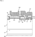
Fig. 1 is a sectional view of a semiconductor device that can be used in a first embodiment of the present invention. -
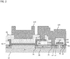
Fig. 2 is an enlarged sectional view of a part ofFig. 1 . -
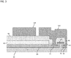
Fig. 3 is a sectional view of the semiconductor device that can be used in the first embodiment of the present invention, and is a sectional view of a part different from a part illustrated inFig. 1 . -
Fig. 4 is a sectional view of a semiconductor device that can be used in a second embodiment of the present invention. -
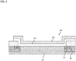
Fig. 5 is a sectional view of a semiconductor device that can be used in a third embodiment of the present invention. -
Fig. 6 is a sectional view of a semiconductor device that can be used in a modification of the third embodiment of the present invention. -
Fig. 7 is a sectional view of a semiconductor device that can be used in a fourth embodiment of the present invention. -
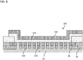
Fig. 8 is a sectional view of a semiconductor device that can be used in a modification of the fourth embodiment of the present invention. - In the present embodiment, description will be given using a vertical MOSFET as one example. Though it is assumed that a first conductivity type is an n type and a second conductivity type is a p type in the description of the present embodiment, the present invention is not limited to that aspect. It may be set such that a first conductivity type is a p type and a second conductivity type is an n type. Further, though the description will be given using silicon carbide as a wide-gap semiconductor in the present embodiment, the present invention is not limited to that aspect. Gallium nitride or the like may be used as a wide-gap semiconductor. In the present embodiment, a vertical direction in
Fig. 1 (a direction along a width of a wide-gap semiconductor device) will be referred to as a vertical direction and a direction perpendicular to the vertical direction will be referred to as an in-plane direction. - As illustrated in
Fig. 1 , a silicon-carbide semiconductor device according to the present embodiment may have an n-type silicon-carbide semiconductor substrate 11, adrift layer 12 that is provided on a first main surface (upper surface) of the silicon-carbide semiconductor substrate 11 and uses an n-type silicon-carbide material, a plurality ofwell regions 20 of a p type provided in thedrift layer 12, and n-type source regions well regions 20. Thewell regions 20 may be formed by implantation of p-type impurities into thedrift layer 12, for example, and thesource regions well regions 20, for example. Adrain electrode 90 may be provided on a second main surface (lower surface) of the silicon-carbide semiconductor substrate 11. A voltage withstanding structure may be provided outside an outer edge of a region to be used as a cell. As thedrain electrode 90, titanium, aluminum, nickel, and the like may be used, for example. - As illustrated in
Fig. 2 , the silicon-carbide semiconductor device may have apolysilicon layer 150 provided on thewell regions 20 and thedrift layer 12 between thewell regions 20, aninterlayer insulating film 65 provided on thepolysilicon layer 150, agate pad 120 provided on theinterlayer insulating film 65, and asource pad 110 electrically connected to thepolysilicon layer 150 via acontact hole 69 provided in theinterlayer insulating film 65. - A
gate insulating film 60 may be provided between a part of theinterlayer insulating film 65, the part being located below thesource pad 110, and each of thewell regions 20, thesource regions drift layer 12. Agate electrode 125 may be provided on thegate insulating film 60 between thesource regions gate electrode 125 may be electrically connected to thegate pad 120. - A
field insulating film 62 may be provided between thewell region 20 and thepolysilicon layer 150. In thewell region 20, at a position below a boundary along an in-plane direction between thefield insulating film 62 and thepolysilicon layer 150, a superhigh-concentration p-type region (p++) 26 may be provided. Thepolysilicon layer 150 may extend and lie over thefield insulating film 62 to form a stepped part. Additionally, the impurity concentration of thewell region 20 in the present embodiment is 5 × 10¹⁶ to 1 × 1019 cm-3, for example, and the impurity concentration of the superhigh-concentration p-type region (including awell contact region 21 described later) is 2 × 10¹⁹ to 1 × 1021 cm-3, for example. - The
polysilicon layer 150 does not need to be provided in all regions below thegate pad 120. As illustrated inFig. 3 , a region where thepolysilicon layer 150 is not provided may exist below thegate pad 120. In that region, thefield insulating film 62 may be provided above thewell region 20 and theinterlayer insulating film 65 may be provided above thefield insulating film 62. - The
drift layer 12 may be formed on the first main surface of the silicon-carbide semiconductor substrate 11 by a CVD process or the like. The n-type impurity concentration of thedrift layer 12 may be lower than the n-type impurity concentration of the silicon-carbide semiconductor substrate 11. Thus, thedrift layer 12 may serve as a low-concentration region (n-) and the silicon-carbide semiconductor substrate 11 may serve as a region having a higher concentration (n) than thedrift layer 12. N, P, and the like can be used as n-type impurities, for example, and Al, B, and the like can be used as p-type impurities, for example. The impurity concentration of thedrift layer 12 in the present embodiment is 1 × 10¹⁴ to 4 × 1016 cm-3, for example, and the impurity concentration of the silicon-carbide semiconductor substrate 11 is 1 × 10¹⁸ to 3 × 1019 cm-3, for example. - The
gate pad 120 may be formed of metal such as Al, for example, and thegate electrode 125 may be formed of polysilicon or the like, for example. Theinterlayer insulating film 65 may be formed on an upper surface of thegate electrode 125 and the like. Thegate electrode 125 may be formed using a CVD process, a photolithography technique, or the like, and theinterlayer insulating film 65 may be formed using a CVD process or the like, and may be formed of silicon dioxide, for example. - In a case where the
gate electrode 125 is formed of polysilicon, thegate electrode 125 and thepolysilicon layer 150 may be formed of the same polysilicon. As polysilicon, undoped polysilicon that is doped with no impurity can be used and also doped silicon that is doped with phosphor, boron, or the like can be used. The terms "the same polysilicon" in the present embodiment mean that both of polysilicon materials are undoped polysilicon or doped polysilicon, and that the kinds and concentrations of impurities doped into doped polysilicon are the same. The terms do not require both of polysilicon materials to be simultaneously manufactured. Thus, even in a case where thegate electrode 125 is formed of polysilicon and thereafter thepolysilicon layer 150 is formed separately, for example, if polysilicon materials used in thegate electrode 125 and thepolysilicon layer 150 are of the same kind (undoped polysilicon or doped polysilicon) and the kinds and concentrations of impurities are the same, thegate electrode 125 and thepolysilicon layer 150 are regarded as being formed of the same polysilicon. - The
gate electrode 125 and thepolysilicon layer 150 may be formed of different kinds of polysilicon. For example, thegate electrode 125 may be formed of doped polysilicon and thepolysilicon layer 150 may be formed of undoped polysilicon. Further, even in a case where both of thegate electrode 125 and thepolysilicon layer 150 are formed of doped polysilicon, n-type doped polysilicon may be used in thegate electrode 125 while p-type doped polysilicon may be used in thepolysilicon layer 150. Conversely, p-type doped polysilicon may be used in thegate electrode 125 while n-type doped polysilicon may be used in thepolysilicon layer 150. Moreover, even in a case where the conductivity types of impurities used in thegate electrode 125 and thepolysilicon layer 150 are the same, that is, an n type or a p type, the concentrations of the impurities may be different. The impurity concentration of doped polysilicon used in thegate electrode 125 may be higher than the impurity concentration of doped polysilicon used in thepolysilicon layer 150. Conversely, the impurity concentration of doped polysilicon used in thegate electrode 125 may be lower than the impurity concentration of doped polysilicon used in thepolysilicon layer 150. - As illustrated in
Fig. 3 , in a section where thepolysilicon layer 150 is not provided, thefield insulating film 62 may be provided on thewell region 20, theinterlayer insulating film 65 may be provided on thefield insulating film 62, and thegate pad 120 may be provided on theinterlayer insulating film 65. Alternatively, thepolysilicon layer 150 may be provided in all regions below thegate pad 120 and thefield insulating film 62 may be absent, unlike those in the above-described aspect. - As illustrated in
Fig. 2 , in thewell region 20, a region (hereinafter also referred to as a "well contactregion 21") that is adjacent to thesource regions source pad 110 may be formed of a superhigh-concentration p-type region (p++). Thesource regions gate electrode 125, and a superhigh-concentration n-type region (n++) 32 provided adjacently to the high-concentration n-type region (n+) 31. Then, thewell contact region 21 may be provided adjacently to the superhigh-concentration n-type region (n++) 32. Ametallic layer 40 formed of nickel, titanium, or alloy containing nickel or titanium may be provided between each of the superhigh-concentration n-type region (n++) 32 in thesource regions well contact region 21, and thesource pad 110. Additionally, in the present embodiment, the impurity concentration of the high-concentration n-type region (n+) is 1 × 10¹⁸ to 2 × 1019 cm-3, for example, and the impurity concentration of the superhigh-concentration n-type region (n++) is 2 × 10¹⁹ to 1 × 1021 cm-3, for example. Further, the high-concentration n-type region (n+) 31 may be absent and the corresponding region may be substituted by the superhigh-concentration n-type region (n++) 32. - Regarding the depth of the
well region 20, a bottom surface thereof is positioned at a level higher than a bottom surface of thedrift layer 12, and thewell region 20 may be provided in thedrift layer 12. Further, regarding the depths of thesource regions well region 20, and thesource regions well region 20. Moreover, regarding the depth of thewell contact region 21, a bottom surface thereof may be positioned at a level higher than a bottom surface of thewell region 20 except thewell contact region 21. - The
polysilicon layer 150 and thedrift layer 12 provided between thewell regions 20 illustrated inFig. 2 may be in Schottky contact. Meanwhile, the superhigh-concentration n-type region (n++) 32 in thesource regions metallic layer 40 provided below thesource pad 110. Further, also thewell contact region 21 that is a superhigh-concentration p-type region (p++) may be in ohmic contact with themetallic layer 40 provided below thesource pad 110. - Next, examples of operation and effect of the present embodiment having the above-described configuration will be described. Note that all aspects described in "Operation and Effects" can be adopted in the above-described configuration.
- In the present embodiment, in a case of adopting an aspect in which the
polysilicon layer 150 electrically connected to thesource pad 110 is provided between thewell regions 20 among thewell regions 20 and thedrift layer 12, theinterlayer insulating film 65 is provided on thepolysilicon layer 150, and thegate pad 120 is provided on theinterlayer insulating film 65 as illustrated inFig. 2 , abnormal increase of a potential in a region below thegate pad 120 can be prevented. - In a case where the p-
type well region 20 is provided in all regions below thesource pad 110, the sheet resistance is 1 kΩ/□ or higher. In contrast thereto, in a case where doped polysilicon is used as thepolysilicon layer 150, the sheet resistance can be reduced to approximately a little over 10 Ω/□, which can suppress potential increase in thewell region 20. - Further, as compared to contact resistance to a region containing p-type impurities in a case where the same metal is in contact with both of a region containing n-type impurities and the region containing p-type impurities in silicon carbide, contact resistance between doped polysilicon and metal is much lower. Thus, also in this respect, potential increase in the
well region 20 can be suppressed. - Further, if a Schottky electrode formed of a metallic material is used below an interlayer insulating film below a gate pad, the manufacturing process thereof is considerably complicated and manufacturing costs therefor are considerably high. In contrast thereto, providing the
polysilicon layer 150 below an interlayer insulating film below a gate pad is advantageous in that the manufacturing process thereof is simplified. - In a case where the
gate electrode 125 is formed of polysilicon and thegate electrode 125 and thepolysilicon layer 150 are formed of the same polysilicon, thepolysilicon layer 150 can be formed simultaneously with formation of thegate electrode 125. This can significantly simplify the manufacturing process thereof. Specifically, thepolysilicon layer 150 can be formed at the time of film formation for thegate electrode 125 formed of polysilicon in a cell part including thesource regions - The
interlayer insulating film 65 may be formed after formation of thegate electrode 125 and thepolysilicon layer 150. Then, when a gate contact hole for connecting thegate pad 120 and thegate electrode 125 is formed in the formedinterlayer insulating film 65, acontact hole 69 also may be formed in a part of theinterlayer insulating film 65, the part being located above thepolysilicon layer 150. Thereafter, thegate pad 120 and thesource pad 110 may be formed, thegate pad 120 and thegate electrode 125 may be electrically connected via the gate contact hole, and thesource pad 110 and thepolysilicon layer 150 may be electrically connected via thecontact hole 69. - Additionally, in view of frequent use of doped polysilicon as the
gate electrode 125, using doped polysilicon as thepolysilicon layer 150 is advantageous. - Next, a second embodiment of the present invention will be described.
- In the present embodiment, as illustrated in
Fig. 4 , p-type regions drift layer 12 betweenwell regions 20. In the present embodiment, in the p-type regions polysilicon layer 150 may be formed of the superhigh-concentration p-type region (p++) 120. In the other respects, this embodiment is similar to the first embodiment and various configurations employed in the first embodiment can be employed also in the second embodiment. The members described in the first embodiment will be described with the same reference signs. - In the present embodiment, the
polysilicon layer 150 and thedrift layer 12 may be in Schottky contact and thepolysilicon layer 150 and the superhigh-concentration p-type region 121 in the p-type regions - In a case where doped polysilicon, or n-type doped polysilicon in particular, is used as the
polysilicon layer 150, a Schottky barrier ϕB is reduced excessively in some cases. In this regard, employing a JBS structure can compensate such reduction of a Schottky barrier ϕB. Particularly, by reducing a pitch in a JBS structure, in other words, by reducing an interval along an in-plane direction between the p-type regions 120 or 121 (setting the interval to approximately 1 to 10 µm, for example), it is possible to more surely compensate reduction of a Schottky barrier ϕB. - In a case where such a JBS structure as in the present embodiment is used, it can be considered to employ the following manufacturing method, for example.
- The p-
type regions type region 120 and the superhigh-concentration p-type region 121 are formed by implantation of p-type impurity ions or the like, thereby forming a JBS structure. Subsequently, processes are performed to form a film of polysilicon. Then, in the film of polysilicon, a part that is to form thegate electrode 125 is left and a part where thepolysilicon layer 150 is to be provided is removed, to form a field opening. - Thereafter, the
polysilicon layer 150 is formed on an upper surface of the JBS structure. On agate electrode 125, polysilicon forming thepolysilicon layer 150 may be further stacked thereon. In order not to leave the stacked polysilicon, thepolysilicon layer 150 may be formed on thegate electrode 125 after thegate electrode 125 is beforehand covered with a mask of an oxide film, for example, and then the mask may be removed after patterning. - Then, an
interlayer insulating film 65 is formed. When a gate contact hole is formed in the formedinterlayer insulating film 65, acontact hole 69 also is formed in a part of theinterlayer insulating film 65, the part being located above thepolysilicon layer 150. - Thereafter, a
gate pad 120 and asource pad 110 are formed, thegate pad 120 and thegate electrode 125 are electrically connected via the gate contact hole, and thesource pad 110 and thepolysilicon layer 150 are electrically connected via thecontact hole 69. - Next, a third embodiment of the present invention will be described.
- In the present embodiment, as illustrated in
Fig. 5 , apolysilicon layer 150 has anundoped polysilicon layer 151 in contact with adrift layer 12, and a dopedpolysilicon layer 152 provided on theundoped polysilicon layer 151. Various configurations employed in the above-described embodiments can be employed also in the third embodiment. The members described in the above embodiments will be described with the same reference signs. - As described above, in a case where doped polysilicon is used as the
polysilicon layer 150, particularly in a case where n-type doped polysilicon is used, a Schottky barrier ϕB is reduced excessively in some cases. In this regard, in the present embodiment, providing theundoped polysilicon layer 151 as a layer in contact with thedrift layer 12 can prevent excessive reduction of a Schottky barrier ϕB. - As described above, in the present embodiment, the aspects in the above-described embodiments can be adopted. Thus, as illustrated in
Fig. 6 , such a JBS structure as in the second embodiment can be employed. More specifically, thepolysilicon layer 150 and thedrift layer 12 may be in Schottky contact and thepolysilicon layer 150 and a superhigh-concentration p-type region 121 in p-type regions - In a case where such a JBS structure as described in the second embodiment is employed in the present embodiment, it can be considered to employ the following manufacturing method, for example.
- The p-
type regions type region 120 and the superhigh-concentration p-type region 121 are formed by implantation of p-type impurity ions or the like, thereby forming a JBS structure. Subsequently, processes are performed to form a film of polysilicon. Then, in the film of polysilicon, a part that is to form agate electrode 125 is left and a part where thepolysilicon layer 150 is to be provided is removed, to form a field opening. - Thereafter, the
undoped polysilicon layer 151 is formed. Then, the dopedpolysilicon layer 152 is formed on theundoped polysilicon layer 151. At that time, on thegate electrode 125, while theundoped polysilicon layer 151 and the dopedpolysilicon layer 152 that form thepolysilicon layer 150 may be formed sequentially, a part of theundoped polysilicon layer 151, the part having been formed on thegate electrode 125, may be removed by etching or the like to reduce influences of theundoped polysilicon layer 151. Alternatively, in thegate electrode 125, only a region in contact with thegate pad 120 may be processed so that theundoped polysilicon layer 151 is not formed there. For example, in thegate electrode 125, theundoped polysilicon layer 151 may be removed only in a region in contact with thegate pad 120. - Moreover, an undoped polysilicon layer having a thickness equal to a total thickness of the
undoped polysilicon layer 151 and the dopedpolysilicon layer 152 may be formed. Then, only a part corresponding to the dopedpolysilicon layer 152 may be doped by ion implantation, for example. - Next, a fourth embodiment of the present invention will be described.
- In the present embodiment, as illustrated in
Fig. 7 , apolysilicon layer 150 has a lightly-dopedpolysilicon layer 153 in contact with adrift layer 12, and a heavily-dopedpolysilicon layer 154 that is provided on the lightly-dopedpolysilicon layer 153 and has an impurity concentration higher than the impurity concentration of the lightly-dopedpolysilicon layer 153. Various configurations employed in the above-described embodiments can be employed also in the fourth embodiment. The members described in the above embodiments will be described with the same reference signs. Additionally, the impurity concentration of the lightly-dopedpolysilicon layer 153 is 1 × 10¹⁵ to 5 × 1018 cm-3, for example, and the impurity concentration of the heavily-dopedpolysilicon layer 154 is 5 × 10¹⁸ to 1 × 1021 cm-3, for example. - Also this embodiment can produce effects similar to those produced by the third embodiment. That is, providing the lightly-doped
polysilicon layer 153 as a layer in contact with thedrift layer 12 can prevent excessive reduction of a Schottky barrier ϕB. - As described above, in the present embodiment, the aspects in the above-described embodiments can be adopted. Thus, as illustrated in
Fig. 8 , such a JBS structure as in the second embodiment can be employed. More specifically, thepolysilicon layer 150 and thedrift layer 12 may be in Schottky contact and thepolysilicon layer 150 and a superhigh-concentration p-type region 121 in p-type regions type regions - The description of each embodiment, the description of the modification, and the disclosure of the drawings described above are merely examples for explaining the invention described in the claims, and the invention described in the claims is not limited by the description of the embodiment or the disclosure of the drawings described above. In addition, the recitation of the claims at the original application is merely an example, and the description of the claims can be appropriately changed based on the description of the specification, the drawings, and the like.
-
- 12 drift layer
- 20 well region
- 21 well contact region
- 26 superhigh-concentration p-type region (superhigh-concentration region of a second conductivity type)
- 62 field insulating film
- 65 interlayer insulating film
- 110 source pad
- 120 gate pad
- 150 polysilicon layer
- 151 undoped polysilicon layer
- 152 doped polysilicon layer
- 153 lightly-doped polysilicon layer
- 154 heavily-doped polysilicon layer
Claims (10)
- A wide gap semiconductor device comprising:a drift layer being a first conductivity type;a plurality of well regions being a second conductivity type and formed in the drift layer;a polysilicon layer provided on the well regions and on the drift layer between the well regions;an interlayer insulating film provided on the polysilicon layer;a gate pad provided on the interlayer insulating film; anda source pad electrically connected to the polysilicon layer.
- The wide gap semiconductor device according to claim 1, wherein
second conductivity type regions are provided at predetermined intervals between the well regions. - The wide gap semiconductor device according to claim 2, wherein
regions in contact with the polysilicon layer in the second conductivity type regions are superhigh-concentration second conductivity regions. - The wide gap semiconductor device according to claim 1, wherein
the polysilicon layer and the drift layer are in Schottky contact. - The wide gap semiconductor device according to claim 1, wherein
a polysilicon layer has an undoped polysilicon layer provided on the drift layer and a doped polysilicon layer provided on the undoped polysilicon layer. - The wide gap semiconductor device according to claim 1, wherein
a polysilicon layer has a lightly-doped polysilicon layer provided on the drift layer, and a heavily-doped polysilicon layer, which is provided on the lightly-doped polysilicon layer and has an impurity concentration higher than the impurity concentration of the lightly-doped polysilicon layer. - The wide gap semiconductor device according to claim 1, wherein
a field insulating film is provided between the well region and the polysilicon layer. - The wide gap semiconductor device according to claim 7, wherein
a superhigh-concentration second conductivity type region is provided in the well region and at a position below a boundary along an in-plane direction between the field insulating film and the polysilicon layer. - The wide gap semiconductor device according to claim 1, wherein
a gate electrode is formed of polysilicon, which constitutes the polysilicon layer. - The wide gap semiconductor device according to claim 1, wherein
a source region is provided in the well region, and
an well contact region, which is adjacent to the source region and is electrically connected to the source pad, in the well region is formed of a superhigh-concentration second conductivity type region.
Applications Claiming Priority (1)
| Application Number | Priority Date | Filing Date | Title |
|---|---|---|---|
| PCT/JP2017/040676 WO2019092871A1 (en) | 2017-11-13 | 2017-11-13 | Wide gap semiconductor device |
Publications (2)
| Publication Number | Publication Date |
|---|---|
| EP3712952A1 true EP3712952A1 (en) | 2020-09-23 |
| EP3712952A4 EP3712952A4 (en) | 2021-06-23 |
Family
ID=66438782
Family Applications (1)
| Application Number | Title | Priority Date | Filing Date |
|---|---|---|---|
| EP17931576.7A Pending EP3712952A4 (en) | 2017-11-13 | 2017-11-13 | Wide gap semiconductor device |
Country Status (6)
| Country | Link |
|---|---|
| US (1) | US11264494B2 (en) |
| EP (1) | EP3712952A4 (en) |
| JP (1) | JP6530567B1 (en) |
| CN (1) | CN111373546B (en) |
| TW (1) | TWI685977B (en) |
| WO (1) | WO2019092871A1 (en) |
Family Cites Families (11)
| Publication number | Priority date | Publication date | Assignee | Title |
|---|---|---|---|---|
| JP2001085705A (en) * | 1999-09-16 | 2001-03-30 | Fuji Electric Co Ltd | Schottky barrier diode manufacturing method |
| US7183575B2 (en) | 2002-02-19 | 2007-02-27 | Nissan Motor Co., Ltd. | High reverse voltage silicon carbide diode and method of manufacturing the same high reverse voltage silicon carbide diode |
| JP4282972B2 (en) | 2002-02-19 | 2009-06-24 | 日産自動車株式会社 | High voltage diode |
| WO2012001837A1 (en) | 2010-06-30 | 2012-01-05 | 三菱電機株式会社 | Power semiconductor device |
| WO2012105609A1 (en) * | 2011-02-02 | 2012-08-09 | ローム株式会社 | Semiconductor device |
| JP6125748B2 (en) * | 2011-12-06 | 2017-05-10 | トヨタ自動車株式会社 | Semiconductor device |
| US9236458B2 (en) * | 2013-07-11 | 2016-01-12 | Infineon Technologies Ag | Bipolar transistor and a method for manufacturing a bipolar transistor |
| JP6244763B2 (en) * | 2013-09-12 | 2017-12-13 | 住友電気工業株式会社 | Silicon carbide semiconductor device |
| JP6424524B2 (en) | 2014-09-08 | 2018-11-21 | 富士電機株式会社 | Semiconductor device and method of manufacturing semiconductor device |
| JP6314867B2 (en) | 2015-02-10 | 2018-04-25 | トヨタ自動車株式会社 | Transmission operation test method |
| DE102015101966B4 (en) * | 2015-02-11 | 2021-07-08 | Infineon Technologies Austria Ag | Method for producing a semiconductor component with Schottky contact and semiconductor component |
-
2017
- 2017-11-13 JP JP2018541226A patent/JP6530567B1/en active Active
- 2017-11-13 WO PCT/JP2017/040676 patent/WO2019092871A1/en not_active Ceased
- 2017-11-13 US US16/763,542 patent/US11264494B2/en active Active
- 2017-11-13 CN CN201780096406.6A patent/CN111373546B/en active Active
- 2017-11-13 EP EP17931576.7A patent/EP3712952A4/en active Pending
-
2018
- 2018-11-12 TW TW107140061A patent/TWI685977B/en active
Also Published As
| Publication number | Publication date |
|---|---|
| US11264494B2 (en) | 2022-03-01 |
| CN111373546B (en) | 2023-12-29 |
| TWI685977B (en) | 2020-02-21 |
| US20200279946A1 (en) | 2020-09-03 |
| WO2019092871A1 (en) | 2019-05-16 |
| JPWO2019092871A1 (en) | 2019-11-14 |
| TW201919245A (en) | 2019-05-16 |
| JP6530567B1 (en) | 2019-06-12 |
| EP3712952A4 (en) | 2021-06-23 |
| CN111373546A (en) | 2020-07-03 |
Similar Documents
| Publication | Publication Date | Title |
|---|---|---|
| US12324203B2 (en) | Method for producing a silicon carbide semiconductor component | |
| DE112013006308B4 (en) | SILICON CARBIDE - SEMICONDUCTOR DEVICE AND METHOD FOR THE PRODUCTION THEREOF | |
| US11081598B2 (en) | Trench MOS Schottky diode | |
| EP2701201A1 (en) | Semiconductor device and method for producing same | |
| US11489071B2 (en) | Semiconductor device | |
| US11881512B2 (en) | Method of manufacturing semiconductor device with silicon carbide body | |
| US10340147B2 (en) | Semiconductor device with equipotential ring contact at curved portion of equipotential ring electrode and method of manufacturing the same | |
| EP3024018B1 (en) | Semiconductor device | |
| CN111712925B (en) | Semiconductor device with a semiconductor device having a plurality of semiconductor chips | |
| EP3159933B1 (en) | Wide-gap semiconductor device and method for manufacturing the same | |
| JP4975618B2 (en) | Device with Schottky junction | |
| CN112466946A (en) | Semiconductor device and method for manufacturing the same | |
| US11056595B2 (en) | Semiconductor device and manufacturing method thereof | |
| US11342435B2 (en) | Wide-gap semiconductor device | |
| US11264494B2 (en) | Wide-gap semiconductor device | |
| EP3832698A1 (en) | Semiconductor device and manufacturing method therefor | |
| JP7808439B2 (en) | diode | |
| CN118588691A (en) | Semiconductor device and method for manufacturing semiconductor device |
Legal Events
| Date | Code | Title | Description |
|---|---|---|---|
| STAA | Information on the status of an ep patent application or granted ep patent |
Free format text: STATUS: THE INTERNATIONAL PUBLICATION HAS BEEN MADE |
|
| PUAI | Public reference made under article 153(3) epc to a published international application that has entered the european phase |
Free format text: ORIGINAL CODE: 0009012 |
|
| STAA | Information on the status of an ep patent application or granted ep patent |
Free format text: STATUS: REQUEST FOR EXAMINATION WAS MADE |
|
| 17P | Request for examination filed |
Effective date: 20200611 |
|
| AK | Designated contracting states |
Kind code of ref document: A1 Designated state(s): AL AT BE BG CH CY CZ DE DK EE ES FI FR GB GR HR HU IE IS IT LI LT LU LV MC MK MT NL NO PL PT RO RS SE SI SK SM TR |
|
| AX | Request for extension of the european patent |
Extension state: BA ME |
|
| DAV | Request for validation of the european patent (deleted) | ||
| DAX | Request for extension of the european patent (deleted) | ||
| A4 | Supplementary search report drawn up and despatched |
Effective date: 20210521 |
|
| RIC1 | Information provided on ipc code assigned before grant |
Ipc: H01L 29/06 20060101AFI20210517BHEP Ipc: H01L 29/12 20060101ALI20210517BHEP Ipc: H01L 29/78 20060101ALI20210517BHEP Ipc: H01L 29/10 20060101ALI20210517BHEP Ipc: H01L 29/16 20060101ALI20210517BHEP Ipc: H01L 29/165 20060101ALI20210517BHEP Ipc: H01L 29/417 20060101ALI20210517BHEP Ipc: H01L 29/66 20060101ALI20210517BHEP |
|
| STAA | Information on the status of an ep patent application or granted ep patent |
Free format text: STATUS: EXAMINATION IS IN PROGRESS |
|
| 17Q | First examination report despatched |
Effective date: 20250612 |