EP3712944A1 - Chip assembly and mold assembly for fabricating same, camera and electronic device - Google Patents
Chip assembly and mold assembly for fabricating same, camera and electronic device Download PDFInfo
- Publication number
- EP3712944A1 EP3712944A1 EP18891020.2A EP18891020A EP3712944A1 EP 3712944 A1 EP3712944 A1 EP 3712944A1 EP 18891020 A EP18891020 A EP 18891020A EP 3712944 A1 EP3712944 A1 EP 3712944A1
- Authority
- EP
- European Patent Office
- Prior art keywords
- chip
- conductive wire
- segment
- circuit board
- chip assembly
- Prior art date
- Legal status (The legal status is an assumption and is not a legal conclusion. Google has not performed a legal analysis and makes no representation as to the accuracy of the status listed.)
- Granted
Links
Images


Classifications
-
- H—ELECTRICITY
- H10—SEMICONDUCTOR DEVICES; ELECTRIC SOLID-STATE DEVICES NOT OTHERWISE PROVIDED FOR
- H10F—INORGANIC SEMICONDUCTOR DEVICES SENSITIVE TO INFRARED RADIATION, LIGHT, ELECTROMAGNETIC RADIATION OF SHORTER WAVELENGTH OR CORPUSCULAR RADIATION
- H10F39/00—Integrated devices, or assemblies of multiple devices, comprising at least one element covered by group H10F30/00, e.g. radiation detectors comprising photodiode arrays
- H10F39/80—Constructional details of image sensors
- H10F39/804—Containers or encapsulations
-
- H—ELECTRICITY
- H04—ELECTRIC COMMUNICATION TECHNIQUE
- H04N—PICTORIAL COMMUNICATION, e.g. TELEVISION
- H04N23/00—Cameras or camera modules comprising electronic image sensors; Control thereof
- H04N23/50—Constructional details
-
- H—ELECTRICITY
- H04—ELECTRIC COMMUNICATION TECHNIQUE
- H04N—PICTORIAL COMMUNICATION, e.g. TELEVISION
- H04N23/00—Cameras or camera modules comprising electronic image sensors; Control thereof
- H04N23/50—Constructional details
- H04N23/54—Mounting of pick-up tubes, electronic image sensors, deviation or focusing coils
-
- H—ELECTRICITY
- H04—ELECTRIC COMMUNICATION TECHNIQUE
- H04N—PICTORIAL COMMUNICATION, e.g. TELEVISION
- H04N23/00—Cameras or camera modules comprising electronic image sensors; Control thereof
- H04N23/56—Cameras or camera modules comprising electronic image sensors; Control thereof provided with illuminating means
-
- H—ELECTRICITY
- H04—ELECTRIC COMMUNICATION TECHNIQUE
- H04N—PICTORIAL COMMUNICATION, e.g. TELEVISION
- H04N23/00—Cameras or camera modules comprising electronic image sensors; Control thereof
- H04N23/57—Mechanical or electrical details of cameras or camera modules specially adapted for being embedded in other devices
-
- H—ELECTRICITY
- H04—ELECTRIC COMMUNICATION TECHNIQUE
- H04N—PICTORIAL COMMUNICATION, e.g. TELEVISION
- H04N23/00—Cameras or camera modules comprising electronic image sensors; Control thereof
- H04N23/90—Arrangement of cameras or camera modules, e.g. multiple cameras in TV studios or sports stadiums
-
- H—ELECTRICITY
- H10—SEMICONDUCTOR DEVICES; ELECTRIC SOLID-STATE DEVICES NOT OTHERWISE PROVIDED FOR
- H10F—INORGANIC SEMICONDUCTOR DEVICES SENSITIVE TO INFRARED RADIATION, LIGHT, ELECTROMAGNETIC RADIATION OF SHORTER WAVELENGTH OR CORPUSCULAR RADIATION
- H10F39/00—Integrated devices, or assemblies of multiple devices, comprising at least one element covered by group H10F30/00, e.g. radiation detectors comprising photodiode arrays
- H10F39/80—Constructional details of image sensors
- H10F39/806—Optical elements or arrangements associated with the image sensors
Definitions
- the present disclosure relates to a technical field of electronic devices, and more particularly, to a chip assembly and a mold assembly for fabricating the same, a camera, and an electronic device.
- a conductive wire 130' is directly provided between a chip 120' and a circuit board 110' of a camera 1' to achieve connection, as illustrated in FIG. 5 .
- This connection method usually encounters a situation that the conductive wire 130' is broken due to various reasons such as post-baking stress, process control, and reliability experiments.
- the conductive wire 130' has a certain curvature, the thickness of the electronic device 1' is increased.
- the present disclosure seeks to solve at least one of the technical problems existing in the related art. To this end, the present disclosure proposes a chip assembly for a camera, and the chip assembly has advantages of a stable structure and a small dimension.
- the present disclosure further proposes a camera including the above chip assembly.
- the present disclosure further proposes an electronic device including the above camera.
- the present disclosure further proposes a mold assembly for fabricating a chip assembly, and the mold assembly has advantages of a simple structure and convenient operation.
- a chip assembly for a camera includes: a circuit board, a chip, and a conductive wire.
- the chip is provided to the circuit board and stacked with the circuit board.
- the conductive wire has a first end electrically coupled to the circuit board and a second end electrically coupled to the chip, a partial segment of the conductive wire is attached to a side wall face of the chip.
- the fixation of the conductive wire can be facilitated, and the installation stability of the conductive wire can be improved. Additionally, it is possible to avoid a situation that the conductive wire is broken due to various reasons such as post-baking stress, process control, and reliability experiments. Moreover, the length of the conductive wire can also be shortened to prevent the conductive wire from forming an arc shape and increasing the thickness of the chip assembly, to reduce the design size of the chip assembly and facilitate the miniaturization design of the camera.
- a camera according to embodiments of the present disclosure includes: a chip assembly configured as the above-mentioned chip assembly.
- the fixation of the conductive wire can be facilitated, and the installation stability of the conductive wire can be improved. Additionally, it is possible to avoid a situation that the conductive wire is broken due to various reasons such as post-baking stress, process control, and reliability experiments. Moreover, the length of the conductive wire can also be shortened to prevent the conductive wire from forming an arc shape and increasing the thickness of the chip assembly, to reduce the design size of the chip assembly and facilitate the miniaturization design of the camera.
- An electronic device includes: a camera configured as the above-mentioned camera.
- the fixation of the conductive wire can be facilitated, and the installation stability of the conductive wire can be improved. Additionally, it is possible to avoid a situation that the conductive wire is broken due to various reasons such as post-baking stress, process control, and reliability experiments. Moreover, the length of the conductive wire can also be shortened to prevent the conductive wire from forming an arc shape and increasing the thickness of the chip assembly, to reduce the design size of the chip assembly and facilitate the miniaturization design of the camera.
- the chip assembly includes a chip, a circuit board, and a conductive wire, and the conductive wire has a first end coupled to the circuit board and a second end coupled to the chip; the mold assembly has an injection cavity and an injection hole in communication with the injection cavity, the chip and the circuit board are located in the injection cavity, the conductive wire is formed by injection molding in the injection hole, and a part of the conductive wire is attached to a side wall face of the chip.
- the fixation of the conductive wire can be facilitated, and the installation stability of the conductive wire can be improved. Additionally, it is possible to avoid a situation that the conductive wire is broken due to various reasons such as post-baking stress, process control, and reliability experiments. Moreover, the length of the conductive wire can also be shortened to prevent the conductive wire from forming an arc shape and increasing the thickness of the chip assembly, so as to reduce the design size of the chip assembly and facilitate the miniaturization design of the camera.
- the terms “mounted,” “connected,” “coupled” or the like are used broadly.
- the terms may be, for example, fixed connections, detachable connections, or integral connections; may also be mechanical or electrical connections, may also be direct connections or indirect connections via intervening structures; and may also be inner communications of two elements, which could be understood by those skilled in the art according to specific situations.
- a chip assembly 100 for a camera 10 includes a circuit board 110, a chip 120, and a conductive wire 130.
- the chip 120 is disposed to the circuit board 110, and the chip 120 and the circuit board 110 are stacked.
- One end of the conductive wire 130 is electrically coupled to the circuit board 110, while the other end of the conductive wire 130 is electrically coupled to the chip 120, and a partial segment of the conductive wire 130 is attached to a side wall face of the chip 120.
- the chip 120 at least partially overlaps with the circuit board 110, the chip 120 may be located on the circuit board 110, and the circuit board 110 may support the chip 120.
- Both ends of the conductive wire 130 may be electrically coupled to the chip 120 and the circuit board 110 respectively, thereby achieving indirect electrical connection between the chip 120 and the circuit board 110.
- a part of the conductive wire 130 may be attached to the side wall face of the chip 120.
- the fixation of the conductive wire 130 can be facilitated, and the installation stability of the conductive wire 130 can be improved, thereby avoiding a situation that the conductive wire 130 is broken due to various reasons such as post-baking stress, process control, and reliability experiments.
- the length of the conductive wire 130 can also be shortened to prevent the conductive wire 130 from forming an arc shape and increasing the thickness of the chip assembly 100, to reduce the design size of the chip assembly 100 and facilitate the miniaturization design of the camera 10.
- the side wall face of the chip 120 may have a groove, and the conductive wire 130 may be embedded in the groove. It could be understood that the side wall face of the chip 120 may be provided with the groove, the groove may penetrate the chip 120 in a thickness direction of the chip 120, and the conductive wire 130 may be disposed in the groove. Therefore, the conductive wire 130 can be positioned in the groove to prevent the conductive wire 130 from being shifted due to external force, which would cause the conductive wire 130 to be broken or to be disconnected with the chip 120 or the circuit board 110.
- the groove can also block part of the external force and prevent the conductive wire 130 from being broken under the external force, to protect the conductive wire 130.
- the circuit board 110 may be provided with a first welding point 111 thereon, and the chip 120 may be provided with a second welding point 121 thereon.
- the second welding point 121 may be located in a position on the chip 120 close to the first welding point 111, and the first welding point 111 may be located in a position on the circuit board 110 close to the second welding point 121.
- a groove may be provided in a side wall face of the chip 120 close to the second welding point 121.
- the groove may be formed as a semi-cylindrical groove, and an axis direction of the semi-cylindrical groove is consistent with the thickness direction of the chip 120.
- a middle segment of the conductive wire 130 can be placed in the groove.
- the conductive wire 130 may be an injection-molded part, and the conductive wire 130 is formed on the side wall face of the chip 120.
- the conductive wire 130 may be formed on the side wall face of the chip 120 by injection molding.
- the conductive wire 130 and the chip 120 can be formed as a whole, and the position of the conductive wire 130 is fixed, the installation of the conductive wire 130 is more stable, and the conductive wire 130 will not be deformed under the action of external force.
- the conductive wire 130 can be formed by injection molding a liquid conductive medium on the side wall face of the chip 120.
- the conductive wire 130 may be a printed circuit. It could be understood that the conductive wire 130 may be etched on the side wall face of the chip 120 by a printing method or a photosensitive process, so that the conductive wire 130 can be quickly drawn directly on a glass plate by an automatic plotter for plate-making, and then be printed.
- the printed circuit can make the mass production of the chip assembly 100 simple and easy, and the printed conductive wires 130 can have consistent performance, stable quality, and compact structures.
- the printed circuit can omit the welding process, thereby improving the production efficiency of the chip assembly 100.
- the printed circuit can achieve high precision, thereby greatly enhancing the production efficiency, stability, and profitability of the circuit board 110.
- the conductive wire 130 may be a gold wire. It could be understood that the conductive wire 130 can be made of gold. Gold has excellent ductility, good stability, small resistivity and good electrical conductivity, and is not easy to generate heat.
- the conductive wire 130 may include a first segment 131 and a second segment 132, wherein the first segment 131 is attached to an upper surface of the circuit board 110, a lower end of the second segment 132 is coupled to the first segment 131, and the second segment 132 is attached to the side wall face of the chip 120.
- the conductive wire 130 may include the first segment 131 and the second segment 132, one end of the first segment 131 is electrically coupled to the circuit board 110, and the other end of the first segment 131 is electrically coupled to one end of the second segment 132; the first segment 131 may be attached to a side surface of the circuit board 110 close to the chip 120, and the second segment 132 may be attached to the side wall face of the chip 120.
- the installation stability of the conductive wire 130 can be enhanced.
- the conductive wire 130 may further include a third segment 133, the third segment 133 is coupled to an upper end of the second segment 132, and the third segment 133 is attached to an upper surface of the chip 120.
- the conductive wire 130 can be arranged in contact with surfaces of the chip 120 and the circuit board 110, thereby preventing the conductive wire 130 from being in a suspended state, to reduce the probability of breakage of the conductive wire 130 and enhance the installation stability of the conductive wire 130.
- the chip 120 may be placed on the upper surface of the circuit board 110 (as illustrated in FIG. 1 ), and the chip 120 may be located at a middle position of the circuit board 110.
- the conductive wire 130 may include the first segment 131, the second segment 132, and the third segment 133.
- the second welding point 121 may be provided on the upper surface of the chip 120 (as illustrated in FIG. 1 ), and the first welding point 111 may be provided on the upper surface of the circuit board 110 (as illustrated in FIG. 1 ).
- first segment 131 may be electrically coupled to the first welding point 111, while the other end of the first segment 131 may be electrically coupled to one end of the second segment 132; the other end of the second segment 132 may be coupled to one end of the third segment 133; the other end of the third segment 133 may be electrically coupled to the second welding point 121.
- the first segment 131 can be attached to the upper surface of the circuit board 110 (as illustrated in FIG. 1 ), the second segment 132 can be attached to the side wall face of the chip 120, and the third segment 133 can be attached to the upper surface of the chip 120 (as illustrated in FIG. 1 ).
- the camera 10 includes a chip assembly, and the chip assembly is the chip assembly 100 as described above.
- the fixation of the conductive wire 130 can be facilitated, and the installation stability of the conductive wire 130 can be improved.
- the length of the conductive wire 130 can also be shortened to prevent the conductive wire 130 from forming an arc shape and increasing the thickness of the chip assembly 100, to reduce the design size of the chip assembly 100 and facilitate the miniaturization design of the camera 10.
- An electronic device 1 includes a camera, and the camera is the camera 10 described above.
- the camera 10 may be embedded in a housing 50 of the electronic device 1.
- the electronic device herein includes, but is not limited to devices for receiving/transmitting a communication signal via a wired line connection (for example, via Public Switched Telephone Network (PSTN), Digital Subscriber Line (DSL), a digital cable, direct cable connection, and/or another data connection/network) and/or via a wireless interface (for example, cellular networks, wireless local area networks (WLANs), digital television networks (such as DVB-H networks), satellite networks, AM-FM broadcast transmitters, and/or another communication terminal).
- PSTN Public Switched Telephone Network
- DSL Digital Subscriber Line
- WLANs wireless local area networks
- DVB-H networks digital television networks
- satellite networks AM-FM broadcast transmitters, and/or another communication terminal
- An electronic device configured to communicate via a wireless interface may be referred to as "a wireless electronic device,” “a wireless device,” and/or “a mobile electronic device.”
- the mobile electronic device include, but are not limited to, satellite or cellular telephones; personal communication system (PCS) devices that may combine cellular radiotelephone with data processing, fax, and data communication capabilities; PDAs that may include radiotelephones, pagers, Internet/Intranet access, web browsers, memo pads, calendars, and/or global positioning system (GPS) receivers; and conventional laptop and/or palmtop receivers or other electronic devices including radiotelephone transceivers.
- PCS personal communication system
- GPS global positioning system
- the fixation of the conductive wire 130 can be facilitated, and the installation stability of the conductive wire 130 can be improved.
- the length of the conductive wire 130 can also be shortened to prevent the conductive wire 130 from forming an arc shape and increasing the thickness of the chip assembly 100, to reduce the design size of the chip assembly 100 and facilitate the miniaturization design of the camera 10.
- the electronic device 1 may be provided with a plurality of cameras 10.
- the plurality of cameras 10 may be electrically coupled, and the plurality of cameras 10 can cooperate with each other for photographing, to improve an imaging effect.
- the electronic device 1 may further include a flash 60.
- the flash 60 may be embedded in the housing 50, and the flash 60 is close to the cameras 10. Therefore, when the cameras 10 are working, the flash 60 can illuminate the subject, thereby improving the photographing effect.
- the chip assembly 100 may include a chip 120, a circuit board 110, and a conductive wire 130.
- One end of the conductive wire 130 is coupled to the circuit board 110, while the other end of the conductive wire 130 is coupled to the chip 120.
- the mold assembly 200 has an injection cavity 210 and an injection hole 220, and the injection hole 220 is in communication with the injection cavity 210.
- the chip 120 and the circuit board 110 are located in the injection cavity 210, and the conductive wire 130 is formed by injection molding in the injection hole 220.
- a part of the conductive wire 130 is attached to a side wall face of the chip 120.
- the injection cavity 210 may be formed inside the mold assembly 200, and the chip 120 and the circuit board 110 may be located in the injection cavity 210.
- the injection hole 220 may be provided through a mold, and one end of the injection hole 220 is in communication with the injection cavity 210 while the other end of the injection hole 220 penetrates the mold assembly 200.
- a conductive medium can be injected from the injection hole 220, so that the conductive wire 130 can be formed on the chip 120 and the circuit board 110.
- One end of the conductive wire 130 can be electrically coupled to the chip 120, while the other end of 130 can be electrically coupled to the circuit board 110.
- a part of the conductive wire 130 can be formed on the side wall face of the chip 120.
- the fixation of the conductive wire 130 can be facilitated, and the installation stability of the conductive wire 130 can be improved.
- the length of the conductive wire 130 can also be shortened to prevent the conductive wire 130 from forming an arc shape and increasing the thickness of the chip assembly 100, to reduce the design size of the chip assembly 100 and facilitate the miniaturization design of the camera 10.
- the chip assembly 100 for the camera 10 will be described in detail below with reference to FIGS. 1-3 .
- the chip 120 may be formed in a rectangular shape, and the circuit board 110 may also be formed in a rectangular shape.
- the chip 120 may be stacked and arranged on the circuit board 110, the chip 120 may be located at a middle position of the circuit board 110, and the circuit board 110 may support the chip 120.
- the surface area of the chip 120 is smaller than the surface area of the circuit board 110.
- the conductive wire 130 may include a first segment 131, a second segment 132, and a third segment 133.
- a second welding point 121 may be provided on an upper surface of the chip 120 (the "up” direction as illustrated in FIG. 1 ), and a first welding point 111 may be provided at a position on the upper surface of the circuit board 110 (the "up” direction as illustrated in FIG. 1 ), which is not in contact with the lower surface of the chip 120 (the "down” direction as illustrated in FIG. 1 ).
- first segment 131 may be electrically coupled to the first welding point 111, the other end of the first segment 131 may be electrically coupled to one end of the second segment 132, the other end of the second segment 132 may be coupled to one end of the third segment 133, and the other end of the third segment 133 is electrically coupled to the second welding point 121.
- the first segment 131 can be attached to the upper surface of the circuit board 110 (the "up" direction as illustrated in FIG. 1 ), the second segment 132 can be attached to the side wall face of the chip 120, and the third segment 133 can be attached to the upper surface of the chip 120 (the "up” direction as illustrated in FIG. 1 ).
- the extension direction of the first segment 131 may be the same as the extension direction of the third segment 133, and the extension direction of the second segment 132 may be perpendicular to the extension direction of the first segment 131.
- the fixation of the conductive wire 130 can be facilitated, and the installation stability of the conductive wire 130 can be improved, thereby avoiding the situation that the conductive wire 130 is broken due to various reasons such as post-baking stress, process control, and reliability experiments.
- the length of the conductive wire 130 can also be shortened to prevent the conductive wire 130 from forming an arc shape and increasing the thickness of the chip assembly 100, to reduce the design size of the chip assembly 100 and facilitate the miniaturization design of the camera 10.
- first and second are used herein for purposes of description and are not intended to indicate or imply relative importance or significance or to imply the number of indicated technical features.
- the feature defined with “first” and “second” may comprise one or more of this feature.
- "a plurality of' means two or more than two, unless specified otherwise.
- a structure in which a first feature is "on" or “below” a second feature may include an embodiment in which the first feature is in direct contact with the second feature, and may also include an embodiment in which the first feature and the second feature are not in direct contact with each other, but are contacted via an additional feature formed therebetween.
- a first feature "on,” “above,” or “on top of' a second feature may include an embodiment in which the first feature is right or obliquely “on,” “above,” or “on top of' the second feature, or just means that the first feature is at a height higher than that of the second feature; while a first feature "below,” “under,” or “on bottom of' a second feature may include an embodiment in which the first feature is right or obliquely “below,” “under,” or “on bottom of' the second feature, or just means that the first feature is at a height lower than that of the second feature.
Landscapes
- Engineering & Computer Science (AREA)
- Multimedia (AREA)
- Signal Processing (AREA)
- Camera Bodies And Camera Details Or Accessories (AREA)
- Studio Devices (AREA)
- Solid State Image Pick-Up Elements (AREA)
Abstract
Description
- The present application claims priority to Chinese Patent Application Serial No.
201711377536.5 - The present application claims priority to Chinese Patent Application Serial No.
201721809499.6 - The present disclosure relates to a technical field of electronic devices, and more particularly, to a chip assembly and a mold assembly for fabricating the same, a camera, and an electronic device.
- As technologies associated with electronic devices develop, electronic devices have a tendency towards miniaturization. As an important part in an electronic device, the design size of the camera is a key technical point to reduce the thickness of the electronic device. In addition, due to external force, connecting wires between a chip and a circuit board in the camera are easy to break. In the related art, generally, a conductive wire 130' is directly provided between a
chip 120' and a circuit board 110' of a camera 1' to achieve connection, as illustrated inFIG. 5 . This connection method usually encounters a situation that the conductive wire 130' is broken due to various reasons such as post-baking stress, process control, and reliability experiments. Moreover, since the conductive wire 130' has a certain curvature, the thickness of the electronic device 1' is increased. - The present disclosure seeks to solve at least one of the technical problems existing in the related art. To this end, the present disclosure proposes a chip assembly for a camera, and the chip assembly has advantages of a stable structure and a small dimension.
- The present disclosure further proposes a camera including the above chip assembly.
- The present disclosure further proposes an electronic device including the above camera.
- The present disclosure further proposes a mold assembly for fabricating a chip assembly, and the mold assembly has advantages of a simple structure and convenient operation.
- A chip assembly for a camera according to embodiments of the present disclosure includes: a circuit board, a chip, and a conductive wire. The chip is provided to the circuit board and stacked with the circuit board. The conductive wire has a first end electrically coupled to the circuit board and a second end electrically coupled to the chip, a partial segment of the conductive wire is attached to a side wall face of the chip.
- For the chip assembly according to the embodiments of the present disclosure, by attaching a part of the conductive wire to the side wall face of the chip, the fixation of the conductive wire can be facilitated, and the installation stability of the conductive wire can be improved. Additionally, it is possible to avoid a situation that the conductive wire is broken due to various reasons such as post-baking stress, process control, and reliability experiments. Moreover, the length of the conductive wire can also be shortened to prevent the conductive wire from forming an arc shape and increasing the thickness of the chip assembly, to reduce the design size of the chip assembly and facilitate the miniaturization design of the camera.
- A camera according to embodiments of the present disclosure includes: a chip assembly configured as the above-mentioned chip assembly.
- For the camera according to the embodiments of the present disclosure, by attaching a part of the conductive wire to the side wall face of the chip, the fixation of the conductive wire can be facilitated, and the installation stability of the conductive wire can be improved. Additionally, it is possible to avoid a situation that the conductive wire is broken due to various reasons such as post-baking stress, process control, and reliability experiments. Moreover, the length of the conductive wire can also be shortened to prevent the conductive wire from forming an arc shape and increasing the thickness of the chip assembly, to reduce the design size of the chip assembly and facilitate the miniaturization design of the camera.
- An electronic device according to embodiments of the present disclosure includes: a camera configured as the above-mentioned camera.
- For the electronic device according to the embodiments of the present disclosure, by attaching a part of the conductive wire to the side wall face of the chip, the fixation of the conductive wire can be facilitated, and the installation stability of the conductive wire can be improved. Additionally, it is possible to avoid a situation that the conductive wire is broken due to various reasons such as post-baking stress, process control, and reliability experiments. Moreover, the length of the conductive wire can also be shortened to prevent the conductive wire from forming an arc shape and increasing the thickness of the chip assembly, to reduce the design size of the chip assembly and facilitate the miniaturization design of the camera.
- Regarding a mold assembly for fabricating a chip assembly according to embodiments of the present disclosure, the chip assembly includes a chip, a circuit board, and a conductive wire, and the conductive wire has a first end coupled to the circuit board and a second end coupled to the chip; the mold assembly has an injection cavity and an injection hole in communication with the injection cavity, the chip and the circuit board are located in the injection cavity, the conductive wire is formed by injection molding in the injection hole, and a part of the conductive wire is attached to a side wall face of the chip.
- For the mold assembly according to the embodiments of the present disclosure, by attaching a part of the conductive wire to the side wall face of the chip, the fixation of the conductive wire can be facilitated, and the installation stability of the conductive wire can be improved. Additionally, it is possible to avoid a situation that the conductive wire is broken due to various reasons such as post-baking stress, process control, and reliability experiments. Moreover, the length of the conductive wire can also be shortened to prevent the conductive wire from forming an arc shape and increasing the thickness of the chip assembly, so as to reduce the design size of the chip assembly and facilitate the miniaturization design of the camera.
- Additional aspects and advantages of embodiments of present disclosure will be given in part in the following descriptions, become apparent in part from the following descriptions, or be learned from the practice of the embodiments of the present disclosure.
- These and/or other aspects and advantages of embodiments of the present disclosure will become apparent and more readily appreciated from the following descriptions of embodiments made with reference to the drawings, in which:
-
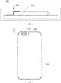
FIG. 1 illustrates a schematic view of a chip assembly for a camera according to an embodiment of the present disclosure. -
FIG. 2 illustrates a schematic view of a chip assembly for a camera according to an embodiment of the present disclosure. -
FIG. 3 illustrates a schematic view of a mold assembly for fabricating a chip assembly according to an embodiment of the present disclosure. -
FIG. 4 illustrates a schematic view of an electronic device according to an embodiment of the present disclosure. -
FIG. 5 illustrates a partial schematic view of an electronic device in the related art. -
-
electronic device 1, -
camera 10, -
chip assembly 100,circuit board 110, first welding point 111,chip 120,second welding point 121, conductive wire 130,first segment 131, second segment 132,third segment 133, -
mold assembly 200,injection cavity 210,injection hole 220, -
housing 50,flash 60, - electronic device 1', camera 10', circuit board 110',
chip 120', conductive wire 130'. - Embodiments of the present disclosure will be described in detail below, and examples of the embodiments will be illustrated in the accompanying drawings. The same or similar reference numerals represent the same or similar elements or the elements having the same or similar functions throughout the descriptions. The embodiments described below with reference to the accompanying drawings are examples, are merely used to explain the present disclosure, and cannot be construed to limit the present disclosure.
- In the description of the present disclosure, it should be understood that terms such as "central," "thickness," "up," "down," "left," "right," "inner," "outer" and the like should be construed to refer to the orientation as then described or as illustrated in the drawings under discussion. These terms are for convenience and simplification of description and do not indicate or imply that the device or element referred to must have a particular orientation, or be constructed and operated in a particular orientation, so these terms shall not be construed to limit the present disclosure. In addition, the feature defined with "first" and "second" may comprise one or more of this feature. In the description of the present disclosure, "a plurality of' means two or more than two, unless specified otherwise.
- In the description of the present disclosure, it should be noted, unless specified or limited otherwise, the terms "mounted," "connected," "coupled" or the like are used broadly. The terms may be, for example, fixed connections, detachable connections, or integral connections; may also be mechanical or electrical connections, may also be direct connections or indirect connections via intervening structures; and may also be inner communications of two elements, which could be understood by those skilled in the art according to specific situations.
- As illustrated in
FIGS. 1-2 , achip assembly 100 for acamera 10 according to embodiments of the present disclosure includes acircuit board 110, achip 120, and a conductive wire 130. - Specifically, referring to
FIGS. 1-2 , thechip 120 is disposed to thecircuit board 110, and thechip 120 and thecircuit board 110 are stacked. One end of the conductive wire 130 is electrically coupled to thecircuit board 110, while the other end of the conductive wire 130 is electrically coupled to thechip 120, and a partial segment of the conductive wire 130 is attached to a side wall face of thechip 120. It could be understood that thechip 120 at least partially overlaps with thecircuit board 110, thechip 120 may be located on thecircuit board 110, and thecircuit board 110 may support thechip 120. Both ends of the conductive wire 130 may be electrically coupled to thechip 120 and thecircuit board 110 respectively, thereby achieving indirect electrical connection between thechip 120 and thecircuit board 110. A part of the conductive wire 130 may be attached to the side wall face of thechip 120. - For the
chip assembly 100 for thecamera 10 according to the embodiments of the present disclosure, by attaching a part of the conductive wire 130 to the side wall face of thechip 120, the fixation of the conductive wire 130 can be facilitated, and the installation stability of the conductive wire 130 can be improved, thereby avoiding a situation that the conductive wire 130 is broken due to various reasons such as post-baking stress, process control, and reliability experiments. In addition, the length of the conductive wire 130 can also be shortened to prevent the conductive wire 130 from forming an arc shape and increasing the thickness of thechip assembly 100, to reduce the design size of thechip assembly 100 and facilitate the miniaturization design of thecamera 10. - According to some embodiments of the present disclosure, the side wall face of the
chip 120 may have a groove, and the conductive wire 130 may be embedded in the groove. It could be understood that the side wall face of thechip 120 may be provided with the groove, the groove may penetrate thechip 120 in a thickness direction of thechip 120, and the conductive wire 130 may be disposed in the groove. Therefore, the conductive wire 130 can be positioned in the groove to prevent the conductive wire 130 from being shifted due to external force, which would cause the conductive wire 130 to be broken or to be disconnected with thechip 120 or thecircuit board 110. The groove can also block part of the external force and prevent the conductive wire 130 from being broken under the external force, to protect the conductive wire 130. - For example, as illustrated in
FIG. 2 , thecircuit board 110 may be provided with a first welding point 111 thereon, and thechip 120 may be provided with asecond welding point 121 thereon. Thesecond welding point 121 may be located in a position on thechip 120 close to the first welding point 111, and the first welding point 111 may be located in a position on thecircuit board 110 close to thesecond welding point 121. A groove may be provided in a side wall face of thechip 120 close to thesecond welding point 121. The groove may be formed as a semi-cylindrical groove, and an axis direction of the semi-cylindrical groove is consistent with the thickness direction of thechip 120. A middle segment of the conductive wire 130 can be placed in the groove. - According to some embodiments of the present disclosure, the conductive wire 130 may be an injection-molded part, and the conductive wire 130 is formed on the side wall face of the
chip 120. In other words, the conductive wire 130 may be formed on the side wall face of thechip 120 by injection molding. As a result, the conductive wire 130 and thechip 120 can be formed as a whole, and the position of the conductive wire 130 is fixed, the installation of the conductive wire 130 is more stable, and the conductive wire 130 will not be deformed under the action of external force. For example, the conductive wire 130 can be formed by injection molding a liquid conductive medium on the side wall face of thechip 120. - According to some embodiments of the present disclosure, the conductive wire 130 may be a printed circuit. It could be understood that the conductive wire 130 may be etched on the side wall face of the
chip 120 by a printing method or a photosensitive process, so that the conductive wire 130 can be quickly drawn directly on a glass plate by an automatic plotter for plate-making, and then be printed. The printed circuit can make the mass production of thechip assembly 100 simple and easy, and the printed conductive wires 130 can have consistent performance, stable quality, and compact structures. The printed circuit can omit the welding process, thereby improving the production efficiency of thechip assembly 100. Moreover, the printed circuit can achieve high precision, thereby greatly enhancing the production efficiency, stability, and profitability of thecircuit board 110. - According to some embodiments of the present disclosure, the conductive wire 130 may be a gold wire. It could be understood that the conductive wire 130 can be made of gold. Gold has excellent ductility, good stability, small resistivity and good electrical conductivity, and is not easy to generate heat.
- As illustrated in
FIG. 1 , according to some embodiments of the present disclosure, the conductive wire 130 may include afirst segment 131 and a second segment 132, wherein thefirst segment 131 is attached to an upper surface of thecircuit board 110, a lower end of the second segment 132 is coupled to thefirst segment 131, and the second segment 132 is attached to the side wall face of thechip 120. It could be understood that the conductive wire 130 may include thefirst segment 131 and the second segment 132, one end of thefirst segment 131 is electrically coupled to thecircuit board 110, and the other end of thefirst segment 131 is electrically coupled to one end of the second segment 132; thefirst segment 131 may be attached to a side surface of thecircuit board 110 close to thechip 120, and the second segment 132 may be attached to the side wall face of thechip 120. Thus, the installation stability of the conductive wire 130 can be enhanced. - Further, as illustrated in
FIG. 1 , the conductive wire 130 may further include athird segment 133, thethird segment 133 is coupled to an upper end of the second segment 132, and thethird segment 133 is attached to an upper surface of thechip 120. As a result, the conductive wire 130 can be arranged in contact with surfaces of thechip 120 and thecircuit board 110, thereby preventing the conductive wire 130 from being in a suspended state, to reduce the probability of breakage of the conductive wire 130 and enhance the installation stability of the conductive wire 130. - For example, as illustrated in
FIGS. 1-2 , thechip 120 may be placed on the upper surface of the circuit board 110 (as illustrated inFIG. 1 ), and thechip 120 may be located at a middle position of thecircuit board 110. The conductive wire 130 may include thefirst segment 131, the second segment 132, and thethird segment 133. Thesecond welding point 121 may be provided on the upper surface of the chip 120 (as illustrated inFIG. 1 ), and the first welding point 111 may be provided on the upper surface of the circuit board 110 (as illustrated inFIG. 1 ). One end of thefirst segment 131 may be electrically coupled to the first welding point 111, while the other end of thefirst segment 131 may be electrically coupled to one end of the second segment 132; the other end of the second segment 132 may be coupled to one end of thethird segment 133; the other end of thethird segment 133 may be electrically coupled to thesecond welding point 121. Thefirst segment 131 can be attached to the upper surface of the circuit board 110 (as illustrated inFIG. 1 ), the second segment 132 can be attached to the side wall face of thechip 120, and thethird segment 133 can be attached to the upper surface of the chip 120 (as illustrated inFIG. 1 ). - The
camera 10 according to embodiments of the present disclosure includes a chip assembly, and the chip assembly is thechip assembly 100 as described above. - For the
camera 10 according to the embodiments of the present disclosure, by attaching a part of the conductive wire 130 to the side wall face of thechip 120, the fixation of the conductive wire 130 can be facilitated, and the installation stability of the conductive wire 130 can be improved. In addition, it is possible to avoid the situation that the conductive wire 130 is broken due to various reasons such as post-baking stress, process control, and reliability experiments. Moreover, the length of the conductive wire 130 can also be shortened to prevent the conductive wire 130 from forming an arc shape and increasing the thickness of thechip assembly 100, to reduce the design size of thechip assembly 100 and facilitate the miniaturization design of thecamera 10. - An
electronic device 1 according to embodiments of the present disclosure includes a camera, and the camera is thecamera 10 described above. Thecamera 10 may be embedded in ahousing 50 of theelectronic device 1. - It should be noted that "the electronic device" herein includes, but is not limited to devices for receiving/transmitting a communication signal via a wired line connection (for example, via Public Switched Telephone Network (PSTN), Digital Subscriber Line (DSL), a digital cable, direct cable connection, and/or another data connection/network) and/or via a wireless interface (for example, cellular networks, wireless local area networks (WLANs), digital television networks (such as DVB-H networks), satellite networks, AM-FM broadcast transmitters, and/or another communication terminal). An electronic device configured to communicate via a wireless interface may be referred to as "a wireless electronic device," "a wireless device," and/or "a mobile electronic device." Examples of the mobile electronic device include, but are not limited to, satellite or cellular telephones; personal communication system (PCS) devices that may combine cellular radiotelephone with data processing, fax, and data communication capabilities; PDAs that may include radiotelephones, pagers, Internet/Intranet access, web browsers, memo pads, calendars, and/or global positioning system (GPS) receivers; and conventional laptop and/or palmtop receivers or other electronic devices including radiotelephone transceivers.
- For the
electronic device 1 according to the embodiments of the present disclosure, by attaching a part of the conductive wire 130 to the side wall face of thechip 120, the fixation of the conductive wire 130 can be facilitated, and the installation stability of the conductive wire 130 can be improved. In addition, it is possible to avoid the situation that the conductive wire 130 is broken due to various reasons such as post-baking stress, process control, and reliability experiments. Moreover, the length of the conductive wire 130 can also be shortened to prevent the conductive wire 130 from forming an arc shape and increasing the thickness of thechip assembly 100, to reduce the design size of thechip assembly 100 and facilitate the miniaturization design of thecamera 10. - Further, the
electronic device 1 may be provided with a plurality ofcameras 10. The plurality ofcameras 10 may be electrically coupled, and the plurality ofcameras 10 can cooperate with each other for photographing, to improve an imaging effect. Furthermore, theelectronic device 1 may further include aflash 60. Theflash 60 may be embedded in thehousing 50, and theflash 60 is close to thecameras 10. Therefore, when thecameras 10 are working, theflash 60 can illuminate the subject, thereby improving the photographing effect. - As illustrated in
FIG. 3 , in amold assembly 200 for fabricating achip assembly 100 according to embodiments of the present disclosure, thechip assembly 100 may include achip 120, acircuit board 110, and a conductive wire 130. One end of the conductive wire 130 is coupled to thecircuit board 110, while the other end of the conductive wire 130 is coupled to thechip 120. Themold assembly 200 has aninjection cavity 210 and aninjection hole 220, and theinjection hole 220 is in communication with theinjection cavity 210. Thechip 120 and thecircuit board 110 are located in theinjection cavity 210, and the conductive wire 130 is formed by injection molding in theinjection hole 220. A part of the conductive wire 130 is attached to a side wall face of thechip 120. - It could be understood that the
injection cavity 210 may be formed inside themold assembly 200, and thechip 120 and thecircuit board 110 may be located in theinjection cavity 210. Theinjection hole 220 may be provided through a mold, and one end of theinjection hole 220 is in communication with theinjection cavity 210 while the other end of theinjection hole 220 penetrates themold assembly 200. A conductive medium can be injected from theinjection hole 220, so that the conductive wire 130 can be formed on thechip 120 and thecircuit board 110. One end of the conductive wire 130 can be electrically coupled to thechip 120, while the other end of 130 can be electrically coupled to thecircuit board 110. A part of the conductive wire 130 can be formed on the side wall face of thechip 120. - For the
mold assembly 200 for fabricating thechip assembly 100 according to the embodiments of the present disclosure, by attaching a part of the conductive wire 130 to the side wall face of thechip 120, the fixation of the conductive wire 130 can be facilitated, and the installation stability of the conductive wire 130 can be improved. In addition, it is possible to avoid the situation that the conductive wire 130 is broken due to various reasons such as post-baking stress, process control, and reliability experiments. Moreover, the length of the conductive wire 130 can also be shortened to prevent the conductive wire 130 from forming an arc shape and increasing the thickness of thechip assembly 100, to reduce the design size of thechip assembly 100 and facilitate the miniaturization design of thecamera 10. - The
chip assembly 100 for thecamera 10 according to the embodiments of the present disclosure will be described in detail below with reference toFIGS. 1-3 . - As illustrated in
FIGS. 1-2 , thechip 120 may be formed in a rectangular shape, and thecircuit board 110 may also be formed in a rectangular shape. Thechip 120 may be stacked and arranged on thecircuit board 110, thechip 120 may be located at a middle position of thecircuit board 110, and thecircuit board 110 may support thechip 120. The surface area of thechip 120 is smaller than the surface area of thecircuit board 110. When thechip 120 is placed on thecircuit board 110, an edge of thechip 120 may be spaced from an edge of thecircuit board 110, and a part of an upper surface of the circuit board 110 (an "up" direction as illustrated inFIG. 1 ) is in contact with a lower surface of the chip 120 (a "down" direction as illustrated inFIG. 1 ). - As illustrated in
FIGS. 1-2 , the conductive wire 130 may include afirst segment 131, a second segment 132, and athird segment 133. Asecond welding point 121 may be provided on an upper surface of the chip 120 (the "up" direction as illustrated inFIG. 1 ), and a first welding point 111 may be provided at a position on the upper surface of the circuit board 110 (the "up" direction as illustrated inFIG. 1 ), which is not in contact with the lower surface of the chip 120 (the "down" direction as illustrated inFIG. 1 ). One end of thefirst segment 131 may be electrically coupled to the first welding point 111, the other end of thefirst segment 131 may be electrically coupled to one end of the second segment 132, the other end of the second segment 132 may be coupled to one end of thethird segment 133, and the other end of thethird segment 133 is electrically coupled to thesecond welding point 121. Thefirst segment 131 can be attached to the upper surface of the circuit board 110 (the "up" direction as illustrated inFIG. 1 ), the second segment 132 can be attached to the side wall face of thechip 120, and thethird segment 133 can be attached to the upper surface of the chip 120 (the "up" direction as illustrated inFIG. 1 ). The extension direction of thefirst segment 131 may be the same as the extension direction of thethird segment 133, and the extension direction of the second segment 132 may be perpendicular to the extension direction of thefirst segment 131. - For the
chip assembly 100 for thecamera 10 according to the embodiments of the present disclosure, by attaching a part of the conductive wire 130 to the side wall face of thechip 120, the fixation of the conductive wire 130 can be facilitated, and the installation stability of the conductive wire 130 can be improved, thereby avoiding the situation that the conductive wire 130 is broken due to various reasons such as post-baking stress, process control, and reliability experiments. In addition, the length of the conductive wire 130 can also be shortened to prevent the conductive wire 130 from forming an arc shape and increasing the thickness of thechip assembly 100, to reduce the design size of thechip assembly 100 and facilitate the miniaturization design of thecamera 10. - In the description of the present disclosure, it should be understood that, terms such as "first" and "second" are used herein for purposes of description and are not intended to indicate or imply relative importance or significance or to imply the number of indicated technical features. Thus, the feature defined with "first" and "second" may comprise one or more of this feature. In the description of the present disclosure, "a plurality of' means two or more than two, unless specified otherwise.
- In the description of the present disclosure, unless specified or limited otherwise, a structure in which a first feature is "on" or "below" a second feature may include an embodiment in which the first feature is in direct contact with the second feature, and may also include an embodiment in which the first feature and the second feature are not in direct contact with each other, but are contacted via an additional feature formed therebetween. Furthermore, a first feature "on," "above," or "on top of' a second feature may include an embodiment in which the first feature is right or obliquely "on," "above," or "on top of' the second feature, or just means that the first feature is at a height higher than that of the second feature; while a first feature "below," "under," or "on bottom of' a second feature may include an embodiment in which the first feature is right or obliquely "below," "under," or "on bottom of' the second feature, or just means that the first feature is at a height lower than that of the second feature.
- Reference throughout this specification to "an embodiment," "some embodiments," "an example", "a specific example," or "some examples," means that a particular feature, structure, material, or characteristic described in connection with the embodiment or example is included in at least one embodiment or example of the present disclosure. Thus, the appearances of the phrases in various places throughout this specification are not necessarily referring to the same embodiment or example of the present disclosure. Moreover, the particular features, structures, materials, or characteristics described may be combined in any suitable manner in one or more embodiments or examples. Moreover, in a case of no contradiction, those skilled in the art may incorporate and combine different embodiments or examples and features of the different embodiments or examples described in this specification.
- Although embodiments of the present disclosure have been illustrated and described above, it could be understood by those skilled in the art that, the above embodiments are examples and cannot be construed to limit the present disclosure, and changes, modifications, alternatives, and variations can be made in the embodiments without departing from the scope of the present disclosure.
Claims (20)
- A chip assembly for a camera, comprising:a circuit board;a chip provided to the circuit board and stacked with the circuit board; anda conductive wire having a first end electrically coupled to the circuit board and a second end electrically coupled to the chip, a partial segment of the conductive wire attached to a side wall face of the chip.
- The chip assembly according to claim 1, wherein the side wall face of the chip has a groove, and the conductive wire is embedded in the groove.
- The chip assembly according to claim 2, wherein the groove is formed as a semi-cylindrical groove.
- The chip assembly according to claim 3, wherein an axis direction of the semi-cylindrical groove is colinear with a thickness direction of the chip.
- The chip assembly according to any one of claims 1 to 4, wherein the conductive wire is an injection-molded part, and the conductive wire is formed on the side wall face of the chip.
- The chip assembly according to any one of claims 1 to 5, wherein the conductive wire is a printed circuit.
- The chip assembly according to any one of claims 1 to 6, wherein the conductive wire is a gold wire.
- The chip assembly according to any one of claims 1 to 7, wherein the conductive wire comprises:a first segment attached to an upper surface of the circuit board; anda second segment having a lower end coupled with the first segment, the second segment attached to the side wall face of the chip.
- The chip assembly according to claim 8, wherein the first segment is perpendicular to the second segment.
- The chip assembly according to claim 8, wherein the conductive wire further comprises:
a third segment coupled with an upper end of the second segment and attached to an upper surface of the chip. - The chip assembly according to claim 10, wherein the third segment is perpendicular to the second segment.
- The chip assembly according to claim 11, wherein the third segment is parallel with the first segment.
- The chip assembly according to any one of claims 1 to 12, wherein the circuit board is provided with a first welding point, and the chip is provided with a second welding point; the second welding point is located in a position on the chip close to the first welding point, and the first welding point is located in a position on the circuit board close to the second welding point; the conductive wire has the first end electrically coupled with the first welding point and the second end electrically coupled with the second welding point.
- A camera, comprising a chip assembly according to any one of claims 1 to 13.
- An electronic device, comprising a camera according to claim 14.
- The electronic device according to claim 15, wherein a plurality of cameras is provided.
- The electronic device according to claim 16, wherein the plurality of cameras is electrically coupled.
- The electronic device according to any one of claims 15 to 17, further comprising a flash close to the camera.
- The electronic device according to any one of claims 15 to 18, further comprising a housing, the camera being embedded in the housing.
- A mold assembly for fabricating a chip assembly, wherein the chip assembly comprises a chip, a circuit board, and a conductive wire, and the conductive wire has a first end coupled to the circuit board and a second end coupled to the chip;
the mold assembly has an injection cavity and an injection hole in communication with the injection cavity, the chip and the circuit board are located in the injection cavity, the conductive wire is formed by injection molding in the injection hole, and a part of the conductive wire is attached to a side wall face of the chip.
Applications Claiming Priority (3)
| Application Number | Priority Date | Filing Date | Title |
|---|---|---|---|
| CN201711377536.5A CN107888815A (en) | 2017-12-19 | 2017-12-19 | Chip assembly and the die assembly, camera and electronic equipment for manufacturing it |
| CN201721809499.6U CN207543219U (en) | 2017-12-19 | 2017-12-19 | Chip assembly and the die assembly, camera and electronic equipment for manufacturing it |
| PCT/CN2018/116206 WO2019120015A1 (en) | 2017-12-19 | 2018-11-19 | Chip assembly and mold assembly for fabricating same, camera and electronic device |
Publications (3)
| Publication Number | Publication Date |
|---|---|
| EP3712944A1 true EP3712944A1 (en) | 2020-09-23 |
| EP3712944A4 EP3712944A4 (en) | 2021-03-03 |
| EP3712944B1 EP3712944B1 (en) | 2023-09-20 |
Family
ID=66992508
Family Applications (1)
| Application Number | Title | Priority Date | Filing Date |
|---|---|---|---|
| EP18891020.2A Active EP3712944B1 (en) | 2017-12-19 | 2018-11-19 | Chip assembly and method of manufacturing the same using a mold assembly, camera and electronic device |
Country Status (3)
| Country | Link |
|---|---|
| US (1) | US11323595B2 (en) |
| EP (1) | EP3712944B1 (en) |
| WO (1) | WO2019120015A1 (en) |
Families Citing this family (1)
| Publication number | Priority date | Publication date | Assignee | Title |
|---|---|---|---|---|
| CN108134898B (en) * | 2018-01-30 | 2020-04-10 | 维沃移动通信有限公司 | Camera module, assembling method of camera module and mobile terminal |
Family Cites Families (12)
| Publication number | Priority date | Publication date | Assignee | Title |
|---|---|---|---|---|
| US20070040932A1 (en) * | 2005-08-19 | 2007-02-22 | Wen-Ching Chen | Image sensor module |
| JP2008124950A (en) * | 2006-11-15 | 2008-05-29 | Alps Electric Co Ltd | Camera module |
| US9136289B2 (en) | 2011-08-23 | 2015-09-15 | Flextronics Ap, Llc | Camera module housing having built-in conductive traces to accommodate stacked dies using flip chip connections |
| CN202307899U (en) * | 2011-11-07 | 2012-07-04 | 江阴长电先进封装有限公司 | Image sensor packaging structure of rivet interconnected structure |
| CN102376733A (en) * | 2011-11-07 | 2012-03-14 | 江阴长电先进封装有限公司 | Image sensor packaging structure with rivet interconnecting structure |
| CN102496622B (en) * | 2011-11-25 | 2016-03-30 | 格科微电子(上海)有限公司 | The method for packing of image sensor chip and camera module |
| US20190148429A1 (en) * | 2016-03-12 | 2019-05-16 | Ningbo Sunny Opotech Co., Ltd. | Camera module, and photosensitive component thereof and manufacturing method therefor |
| CN205754556U (en) | 2016-05-19 | 2016-11-30 | 江西盛泰光学有限公司 | A kind of cell-phone camera header structure |
| CN107888812A (en) * | 2017-11-27 | 2018-04-06 | 维沃移动通信有限公司 | The camera module of a kind of electronic equipment and electronic equipment |
| CN107888815A (en) * | 2017-12-19 | 2018-04-06 | 广东欧珀移动通信有限公司 | Chip assembly and the die assembly, camera and electronic equipment for manufacturing it |
| CN207543219U (en) * | 2017-12-19 | 2018-06-26 | 广东欧珀移动通信有限公司 | Chip assembly and the die assembly, camera and electronic equipment for manufacturing it |
| US10910336B2 (en) * | 2019-01-29 | 2021-02-02 | Shih-Chi Chen | Chip package structure |
-
2018
- 2018-11-19 EP EP18891020.2A patent/EP3712944B1/en active Active
- 2018-11-19 WO PCT/CN2018/116206 patent/WO2019120015A1/en not_active Ceased
- 2018-11-19 US US16/769,870 patent/US11323595B2/en active Active
Also Published As
| Publication number | Publication date |
|---|---|
| US11323595B2 (en) | 2022-05-03 |
| EP3712944B1 (en) | 2023-09-20 |
| WO2019120015A1 (en) | 2019-06-27 |
| EP3712944A4 (en) | 2021-03-03 |
| US20210185192A1 (en) | 2021-06-17 |
Similar Documents
| Publication | Publication Date | Title |
|---|---|---|
| US20190027813A1 (en) | Method for manufacturing rear cover, rear cover and electronic device having the same | |
| CN108322574A (en) | Display screen, terminal display screen component and mobile terminal | |
| TW201543754A (en) | Cable connector assembly for a communication system | |
| EP1677387A1 (en) | Built-in antenna module including a bluetooth radiator in portable wireless terminal | |
| CN108881534B (en) | Display screen assembly and electronic equipment | |
| CN108429838A (en) | Display components and electronic equipment | |
| US11323595B2 (en) | Chip assembly, camera and electronic device | |
| CN207543219U (en) | Chip assembly and the die assembly, camera and electronic equipment for manufacturing it | |
| EP3993387A1 (en) | Base, camera module and electronic device | |
| CN113437550B (en) | Electronic equipment | |
| CN107888815A (en) | Chip assembly and the die assembly, camera and electronic equipment for manufacturing it | |
| CN108322573B (en) | Display screen assembly and electronic equipment | |
| CN112018505B (en) | Antenna shrapnel, antenna components and electronics | |
| CN106452494A (en) | Waterproof jacket for thimble, shell component and terminal | |
| CN206650701U (en) | Housing unit and there is its terminal | |
| EP4016982A1 (en) | Base, camera module, and electronic device | |
| CN107888729A (en) | Bracket component, camera and electronic equipment | |
| US20070035455A1 (en) | Display frame having antenna | |
| CN107147835B (en) | electronic device | |
| CN110299613A (en) | Mobile terminal | |
| CN207427239U (en) | Bracket component, camera and electronic equipment | |
| CN208127410U (en) | Antenna connection component, antenna and mobile terminal | |
| KR20100016841A (en) | Mobile communication terminal case and mobile communication terminal | |
| CN109067952B (en) | Mobile terminal device and receiver assembly thereof | |
| CN107749525B (en) | Earphone socket, mounting structure and mobile terminal |
Legal Events
| Date | Code | Title | Description |
|---|---|---|---|
| STAA | Information on the status of an ep patent application or granted ep patent |
Free format text: STATUS: THE INTERNATIONAL PUBLICATION HAS BEEN MADE |
|
| PUAI | Public reference made under article 153(3) epc to a published international application that has entered the european phase |
Free format text: ORIGINAL CODE: 0009012 |
|
| STAA | Information on the status of an ep patent application or granted ep patent |
Free format text: STATUS: REQUEST FOR EXAMINATION WAS MADE |
|
| 17P | Request for examination filed |
Effective date: 20200617 |
|
| AK | Designated contracting states |
Kind code of ref document: A1 Designated state(s): AL AT BE BG CH CY CZ DE DK EE ES FI FR GB GR HR HU IE IS IT LI LT LU LV MC MK MT NL NO PL PT RO RS SE SI SK SM TR |
|
| AX | Request for extension of the european patent |
Extension state: BA ME |
|
| A4 | Supplementary search report drawn up and despatched |
Effective date: 20210202 |
|
| RIC1 | Information provided on ipc code assigned before grant |
Ipc: H01L 27/146 20060101AFI20210127BHEP Ipc: H04N 5/225 20060101ALI20210127BHEP |
|
| DAV | Request for validation of the european patent (deleted) | ||
| DAX | Request for extension of the european patent (deleted) | ||
| RIC1 | Information provided on ipc code assigned before grant |
Ipc: H01L 27/146 20060101AFI20230220BHEP |
|
| GRAP | Despatch of communication of intention to grant a patent |
Free format text: ORIGINAL CODE: EPIDOSNIGR1 |
|
| STAA | Information on the status of an ep patent application or granted ep patent |
Free format text: STATUS: GRANT OF PATENT IS INTENDED |
|
| INTG | Intention to grant announced |
Effective date: 20230414 |
|
| GRAS | Grant fee paid |
Free format text: ORIGINAL CODE: EPIDOSNIGR3 |
|
| GRAA | (expected) grant |
Free format text: ORIGINAL CODE: 0009210 |
|
| STAA | Information on the status of an ep patent application or granted ep patent |
Free format text: STATUS: THE PATENT HAS BEEN GRANTED |
|
| AK | Designated contracting states |
Kind code of ref document: B1 Designated state(s): AL AT BE BG CH CY CZ DE DK EE ES FI FR GB GR HR HU IE IS IT LI LT LU LV MC MK MT NL NO PL PT RO RS SE SI SK SM TR |
|
| REG | Reference to a national code |
Ref country code: GB Ref legal event code: FG4D |
|
| REG | Reference to a national code |
Ref country code: CH Ref legal event code: EP |
|
| REG | Reference to a national code |
Ref country code: IE Ref legal event code: FG4D |
|
| REG | Reference to a national code |
Ref country code: DE Ref legal event code: R096 Ref document number: 602018058079 Country of ref document: DE |
|
| P01 | Opt-out of the competence of the unified patent court (upc) registered |
Effective date: 20231016 |
|
| REG | Reference to a national code |
Ref country code: LT Ref legal event code: MG9D |
|
| PG25 | Lapsed in a contracting state [announced via postgrant information from national office to epo] |
Ref country code: GR Free format text: LAPSE BECAUSE OF FAILURE TO SUBMIT A TRANSLATION OF THE DESCRIPTION OR TO PAY THE FEE WITHIN THE PRESCRIBED TIME-LIMIT Effective date: 20231221 |
|
| REG | Reference to a national code |
Ref country code: NL Ref legal event code: MP Effective date: 20230920 |
|
| PG25 | Lapsed in a contracting state [announced via postgrant information from national office to epo] |
Ref country code: SE Free format text: LAPSE BECAUSE OF FAILURE TO SUBMIT A TRANSLATION OF THE DESCRIPTION OR TO PAY THE FEE WITHIN THE PRESCRIBED TIME-LIMIT Effective date: 20230920 Ref country code: RS Free format text: LAPSE BECAUSE OF FAILURE TO SUBMIT A TRANSLATION OF THE DESCRIPTION OR TO PAY THE FEE WITHIN THE PRESCRIBED TIME-LIMIT Effective date: 20230920 Ref country code: NO Free format text: LAPSE BECAUSE OF FAILURE TO SUBMIT A TRANSLATION OF THE DESCRIPTION OR TO PAY THE FEE WITHIN THE PRESCRIBED TIME-LIMIT Effective date: 20231220 Ref country code: LV Free format text: LAPSE BECAUSE OF FAILURE TO SUBMIT A TRANSLATION OF THE DESCRIPTION OR TO PAY THE FEE WITHIN THE PRESCRIBED TIME-LIMIT Effective date: 20230920 Ref country code: LT Free format text: LAPSE BECAUSE OF FAILURE TO SUBMIT A TRANSLATION OF THE DESCRIPTION OR TO PAY THE FEE WITHIN THE PRESCRIBED TIME-LIMIT Effective date: 20230920 Ref country code: HR Free format text: LAPSE BECAUSE OF FAILURE TO SUBMIT A TRANSLATION OF THE DESCRIPTION OR TO PAY THE FEE WITHIN THE PRESCRIBED TIME-LIMIT Effective date: 20230920 Ref country code: GR Free format text: LAPSE BECAUSE OF FAILURE TO SUBMIT A TRANSLATION OF THE DESCRIPTION OR TO PAY THE FEE WITHIN THE PRESCRIBED TIME-LIMIT Effective date: 20231221 Ref country code: FI Free format text: LAPSE BECAUSE OF FAILURE TO SUBMIT A TRANSLATION OF THE DESCRIPTION OR TO PAY THE FEE WITHIN THE PRESCRIBED TIME-LIMIT Effective date: 20230920 |
|
| REG | Reference to a national code |
Ref country code: AT Ref legal event code: MK05 Ref document number: 1614097 Country of ref document: AT Kind code of ref document: T Effective date: 20230920 |
|
| PG25 | Lapsed in a contracting state [announced via postgrant information from national office to epo] |
Ref country code: NL Free format text: LAPSE BECAUSE OF FAILURE TO SUBMIT A TRANSLATION OF THE DESCRIPTION OR TO PAY THE FEE WITHIN THE PRESCRIBED TIME-LIMIT Effective date: 20230920 |
|
| PG25 | Lapsed in a contracting state [announced via postgrant information from national office to epo] |
Ref country code: IS Free format text: LAPSE BECAUSE OF FAILURE TO SUBMIT A TRANSLATION OF THE DESCRIPTION OR TO PAY THE FEE WITHIN THE PRESCRIBED TIME-LIMIT Effective date: 20240120 |
|
| PG25 | Lapsed in a contracting state [announced via postgrant information from national office to epo] |
Ref country code: AT Free format text: LAPSE BECAUSE OF FAILURE TO SUBMIT A TRANSLATION OF THE DESCRIPTION OR TO PAY THE FEE WITHIN THE PRESCRIBED TIME-LIMIT Effective date: 20230920 |
|
| PG25 | Lapsed in a contracting state [announced via postgrant information from national office to epo] |
Ref country code: ES Free format text: LAPSE BECAUSE OF FAILURE TO SUBMIT A TRANSLATION OF THE DESCRIPTION OR TO PAY THE FEE WITHIN THE PRESCRIBED TIME-LIMIT Effective date: 20230920 |
|
| PG25 | Lapsed in a contracting state [announced via postgrant information from national office to epo] |
Ref country code: SM Free format text: LAPSE BECAUSE OF FAILURE TO SUBMIT A TRANSLATION OF THE DESCRIPTION OR TO PAY THE FEE WITHIN THE PRESCRIBED TIME-LIMIT Effective date: 20230920 Ref country code: RO Free format text: LAPSE BECAUSE OF FAILURE TO SUBMIT A TRANSLATION OF THE DESCRIPTION OR TO PAY THE FEE WITHIN THE PRESCRIBED TIME-LIMIT Effective date: 20230920 Ref country code: IS Free format text: LAPSE BECAUSE OF FAILURE TO SUBMIT A TRANSLATION OF THE DESCRIPTION OR TO PAY THE FEE WITHIN THE PRESCRIBED TIME-LIMIT Effective date: 20240120 Ref country code: ES Free format text: LAPSE BECAUSE OF FAILURE TO SUBMIT A TRANSLATION OF THE DESCRIPTION OR TO PAY THE FEE WITHIN THE PRESCRIBED TIME-LIMIT Effective date: 20230920 Ref country code: EE Free format text: LAPSE BECAUSE OF FAILURE TO SUBMIT A TRANSLATION OF THE DESCRIPTION OR TO PAY THE FEE WITHIN THE PRESCRIBED TIME-LIMIT Effective date: 20230920 Ref country code: CZ Free format text: LAPSE BECAUSE OF FAILURE TO SUBMIT A TRANSLATION OF THE DESCRIPTION OR TO PAY THE FEE WITHIN THE PRESCRIBED TIME-LIMIT Effective date: 20230920 Ref country code: AT Free format text: LAPSE BECAUSE OF FAILURE TO SUBMIT A TRANSLATION OF THE DESCRIPTION OR TO PAY THE FEE WITHIN THE PRESCRIBED TIME-LIMIT Effective date: 20230920 Ref country code: PT Free format text: LAPSE BECAUSE OF FAILURE TO SUBMIT A TRANSLATION OF THE DESCRIPTION OR TO PAY THE FEE WITHIN THE PRESCRIBED TIME-LIMIT Effective date: 20240122 Ref country code: SK Free format text: LAPSE BECAUSE OF FAILURE TO SUBMIT A TRANSLATION OF THE DESCRIPTION OR TO PAY THE FEE WITHIN THE PRESCRIBED TIME-LIMIT Effective date: 20230920 |
|
| PG25 | Lapsed in a contracting state [announced via postgrant information from national office to epo] |
Ref country code: PL Free format text: LAPSE BECAUSE OF FAILURE TO SUBMIT A TRANSLATION OF THE DESCRIPTION OR TO PAY THE FEE WITHIN THE PRESCRIBED TIME-LIMIT Effective date: 20230920 Ref country code: IT Free format text: LAPSE BECAUSE OF FAILURE TO SUBMIT A TRANSLATION OF THE DESCRIPTION OR TO PAY THE FEE WITHIN THE PRESCRIBED TIME-LIMIT Effective date: 20230920 |
|
| REG | Reference to a national code |
Ref country code: DE Ref legal event code: R097 Ref document number: 602018058079 Country of ref document: DE |
|
| REG | Reference to a national code |
Ref country code: CH Ref legal event code: PL |
|
| PG25 | Lapsed in a contracting state [announced via postgrant information from national office to epo] |
Ref country code: MC Free format text: LAPSE BECAUSE OF FAILURE TO SUBMIT A TRANSLATION OF THE DESCRIPTION OR TO PAY THE FEE WITHIN THE PRESCRIBED TIME-LIMIT Effective date: 20230920 |
|
| PG25 | Lapsed in a contracting state [announced via postgrant information from national office to epo] |
Ref country code: DK Free format text: LAPSE BECAUSE OF FAILURE TO SUBMIT A TRANSLATION OF THE DESCRIPTION OR TO PAY THE FEE WITHIN THE PRESCRIBED TIME-LIMIT Effective date: 20230920 |
|
| PG25 | Lapsed in a contracting state [announced via postgrant information from national office to epo] |
Ref country code: LU Free format text: LAPSE BECAUSE OF NON-PAYMENT OF DUE FEES Effective date: 20231119 |
|
| PG25 | Lapsed in a contracting state [announced via postgrant information from national office to epo] |
Ref country code: CH Free format text: LAPSE BECAUSE OF NON-PAYMENT OF DUE FEES Effective date: 20231130 |
|
| PLBE | No opposition filed within time limit |
Free format text: ORIGINAL CODE: 0009261 |
|
| STAA | Information on the status of an ep patent application or granted ep patent |
Free format text: STATUS: NO OPPOSITION FILED WITHIN TIME LIMIT |
|
| PG25 | Lapsed in a contracting state [announced via postgrant information from national office to epo] |
Ref country code: MC Free format text: LAPSE BECAUSE OF FAILURE TO SUBMIT A TRANSLATION OF THE DESCRIPTION OR TO PAY THE FEE WITHIN THE PRESCRIBED TIME-LIMIT Effective date: 20230920 Ref country code: LU Free format text: LAPSE BECAUSE OF NON-PAYMENT OF DUE FEES Effective date: 20231119 Ref country code: DK Free format text: LAPSE BECAUSE OF FAILURE TO SUBMIT A TRANSLATION OF THE DESCRIPTION OR TO PAY THE FEE WITHIN THE PRESCRIBED TIME-LIMIT Effective date: 20230920 Ref country code: CH Free format text: LAPSE BECAUSE OF NON-PAYMENT OF DUE FEES Effective date: 20231130 |
|
| REG | Reference to a national code |
Ref country code: BE Ref legal event code: MM Effective date: 20231130 |
|
| 26N | No opposition filed |
Effective date: 20240621 |
|
| REG | Reference to a national code |
Ref country code: IE Ref legal event code: MM4A |
|
| PG25 | Lapsed in a contracting state [announced via postgrant information from national office to epo] |
Ref country code: IE Free format text: LAPSE BECAUSE OF NON-PAYMENT OF DUE FEES Effective date: 20231119 |
|
| PG25 | Lapsed in a contracting state [announced via postgrant information from national office to epo] |
Ref country code: BE Free format text: LAPSE BECAUSE OF NON-PAYMENT OF DUE FEES Effective date: 20231130 |
|
| PG25 | Lapsed in a contracting state [announced via postgrant information from national office to epo] |
Ref country code: FR Free format text: LAPSE BECAUSE OF NON-PAYMENT OF DUE FEES Effective date: 20231120 |
|
| PG25 | Lapsed in a contracting state [announced via postgrant information from national office to epo] |
Ref country code: SI Free format text: LAPSE BECAUSE OF FAILURE TO SUBMIT A TRANSLATION OF THE DESCRIPTION OR TO PAY THE FEE WITHIN THE PRESCRIBED TIME-LIMIT Effective date: 20230920 |
|
| PG25 | Lapsed in a contracting state [announced via postgrant information from national office to epo] |
Ref country code: SI Free format text: LAPSE BECAUSE OF FAILURE TO SUBMIT A TRANSLATION OF THE DESCRIPTION OR TO PAY THE FEE WITHIN THE PRESCRIBED TIME-LIMIT Effective date: 20230920 Ref country code: IE Free format text: LAPSE BECAUSE OF NON-PAYMENT OF DUE FEES Effective date: 20231119 Ref country code: FR Free format text: LAPSE BECAUSE OF NON-PAYMENT OF DUE FEES Effective date: 20231120 Ref country code: BE Free format text: LAPSE BECAUSE OF NON-PAYMENT OF DUE FEES Effective date: 20231130 |
|
| PG25 | Lapsed in a contracting state [announced via postgrant information from national office to epo] |
Ref country code: BG Free format text: LAPSE BECAUSE OF FAILURE TO SUBMIT A TRANSLATION OF THE DESCRIPTION OR TO PAY THE FEE WITHIN THE PRESCRIBED TIME-LIMIT Effective date: 20230920 |
|
| REG | Reference to a national code |
Ref country code: DE Ref legal event code: R079 Ref document number: 602018058079 Country of ref document: DE Free format text: PREVIOUS MAIN CLASS: H01L0027146000 Ipc: H10F0039180000 |
|
| PG25 | Lapsed in a contracting state [announced via postgrant information from national office to epo] |
Ref country code: BG Free format text: LAPSE BECAUSE OF FAILURE TO SUBMIT A TRANSLATION OF THE DESCRIPTION OR TO PAY THE FEE WITHIN THE PRESCRIBED TIME-LIMIT Effective date: 20230920 |
|
| PG25 | Lapsed in a contracting state [announced via postgrant information from national office to epo] |
Ref country code: CY Free format text: LAPSE BECAUSE OF FAILURE TO SUBMIT A TRANSLATION OF THE DESCRIPTION OR TO PAY THE FEE WITHIN THE PRESCRIBED TIME-LIMIT; INVALID AB INITIO Effective date: 20181119 |
|
| PG25 | Lapsed in a contracting state [announced via postgrant information from national office to epo] |
Ref country code: HU Free format text: LAPSE BECAUSE OF FAILURE TO SUBMIT A TRANSLATION OF THE DESCRIPTION OR TO PAY THE FEE WITHIN THE PRESCRIBED TIME-LIMIT; INVALID AB INITIO Effective date: 20181119 |
|
| PG25 | Lapsed in a contracting state [announced via postgrant information from national office to epo] |
Ref country code: TR Free format text: LAPSE BECAUSE OF FAILURE TO SUBMIT A TRANSLATION OF THE DESCRIPTION OR TO PAY THE FEE WITHIN THE PRESCRIBED TIME-LIMIT Effective date: 20230920 |
|
| PGFP | Annual fee paid to national office [announced via postgrant information from national office to epo] |
Ref country code: DE Payment date: 20251124 Year of fee payment: 8 |
|
| PGFP | Annual fee paid to national office [announced via postgrant information from national office to epo] |
Ref country code: GB Payment date: 20251126 Year of fee payment: 8 |