EP3712675A1 - Dual-axis semiconductor micromirror - Google Patents
Dual-axis semiconductor micromirror Download PDFInfo
- Publication number
- EP3712675A1 EP3712675A1 EP19194327.3A EP19194327A EP3712675A1 EP 3712675 A1 EP3712675 A1 EP 3712675A1 EP 19194327 A EP19194327 A EP 19194327A EP 3712675 A1 EP3712675 A1 EP 3712675A1
- Authority
- EP
- European Patent Office
- Prior art keywords
- actuator
- connection member
- frame
- stage
- semiconductor device
- Prior art date
- Legal status (The legal status is an assumption and is not a legal conclusion. Google has not performed a legal analysis and makes no representation as to the accuracy of the status listed.)
- Withdrawn
Links
Images




Classifications
-
- G—PHYSICS
- G02—OPTICS
- G02B—OPTICAL ELEMENTS, SYSTEMS OR APPARATUS
- G02B26/00—Optical devices or arrangements for the control of light using movable or deformable optical elements
- G02B26/08—Optical devices or arrangements for the control of light using movable or deformable optical elements for controlling the direction of light
- G02B26/0816—Optical devices or arrangements for the control of light using movable or deformable optical elements for controlling the direction of light by means of one or more reflecting elements
- G02B26/0833—Optical devices or arrangements for the control of light using movable or deformable optical elements for controlling the direction of light by means of one or more reflecting elements the reflecting element being a micromechanical device, e.g. a MEMS mirror, DMD
- G02B26/0858—Optical devices or arrangements for the control of light using movable or deformable optical elements for controlling the direction of light by means of one or more reflecting elements the reflecting element being a micromechanical device, e.g. a MEMS mirror, DMD the reflecting means being moved or deformed by piezoelectric means
-
- B—PERFORMING OPERATIONS; TRANSPORTING
- B81—MICROSTRUCTURAL TECHNOLOGY
- B81B—MICROSTRUCTURAL DEVICES OR SYSTEMS, e.g. MICROMECHANICAL DEVICES
- B81B3/00—Devices comprising flexible or deformable elements, e.g. comprising elastic tongues or membranes
- B81B3/0018—Structures acting upon the moving or flexible element for transforming energy into mechanical movement or vice versa, i.e. actuators, sensors, generators
- B81B3/0024—Transducers for transforming thermal into mechanical energy or vice versa, e.g. thermal or bimorph actuators
-
- B—PERFORMING OPERATIONS; TRANSPORTING
- B81—MICROSTRUCTURAL TECHNOLOGY
- B81B—MICROSTRUCTURAL DEVICES OR SYSTEMS, e.g. MICROMECHANICAL DEVICES
- B81B3/00—Devices comprising flexible or deformable elements, e.g. comprising elastic tongues or membranes
- B81B3/0062—Devices moving in two or more dimensions, i.e. having special features which allow movement in more than one dimension
-
- G—PHYSICS
- G02—OPTICS
- G02B—OPTICAL ELEMENTS, SYSTEMS OR APPARATUS
- G02B26/00—Optical devices or arrangements for the control of light using movable or deformable optical elements
- G02B26/08—Optical devices or arrangements for the control of light using movable or deformable optical elements for controlling the direction of light
- G02B26/0816—Optical devices or arrangements for the control of light using movable or deformable optical elements for controlling the direction of light by means of one or more reflecting elements
- G02B26/0833—Optical devices or arrangements for the control of light using movable or deformable optical elements for controlling the direction of light by means of one or more reflecting elements the reflecting element being a micromechanical device, e.g. a MEMS mirror, DMD
- G02B26/0866—Optical devices or arrangements for the control of light using movable or deformable optical elements for controlling the direction of light by means of one or more reflecting elements the reflecting element being a micromechanical device, e.g. a MEMS mirror, DMD the reflecting means being moved or deformed by thermal means
-
- G—PHYSICS
- G02—OPTICS
- G02B—OPTICAL ELEMENTS, SYSTEMS OR APPARATUS
- G02B26/00—Optical devices or arrangements for the control of light using movable or deformable optical elements
- G02B26/08—Optical devices or arrangements for the control of light using movable or deformable optical elements for controlling the direction of light
- G02B26/10—Scanning systems
- G02B26/101—Scanning systems with both horizontal and vertical deflecting means, e.g. raster or XY scanners
-
- G—PHYSICS
- G02—OPTICS
- G02B—OPTICAL ELEMENTS, SYSTEMS OR APPARATUS
- G02B26/00—Optical devices or arrangements for the control of light using movable or deformable optical elements
- G02B26/08—Optical devices or arrangements for the control of light using movable or deformable optical elements for controlling the direction of light
- G02B26/10—Scanning systems
- G02B26/105—Scanning systems with one or more pivoting mirrors or galvano-mirrors
-
- B—PERFORMING OPERATIONS; TRANSPORTING
- B81—MICROSTRUCTURAL TECHNOLOGY
- B81B—MICROSTRUCTURAL DEVICES OR SYSTEMS, e.g. MICROMECHANICAL DEVICES
- B81B2201/00—Specific applications of microelectromechanical systems
- B81B2201/03—Microengines and actuators
- B81B2201/031—Thermal actuators
-
- B—PERFORMING OPERATIONS; TRANSPORTING
- B81—MICROSTRUCTURAL TECHNOLOGY
- B81B—MICROSTRUCTURAL DEVICES OR SYSTEMS, e.g. MICROMECHANICAL DEVICES
- B81B2201/00—Specific applications of microelectromechanical systems
- B81B2201/03—Microengines and actuators
- B81B2201/032—Bimorph and unimorph actuators, e.g. piezo and thermo
-
- B—PERFORMING OPERATIONS; TRANSPORTING
- B81—MICROSTRUCTURAL TECHNOLOGY
- B81B—MICROSTRUCTURAL DEVICES OR SYSTEMS, e.g. MICROMECHANICAL DEVICES
- B81B2201/00—Specific applications of microelectromechanical systems
- B81B2201/04—Optical MEMS
- B81B2201/042—Micromirrors, not used as optical switches
-
- B—PERFORMING OPERATIONS; TRANSPORTING
- B81—MICROSTRUCTURAL TECHNOLOGY
- B81B—MICROSTRUCTURAL DEVICES OR SYSTEMS, e.g. MICROMECHANICAL DEVICES
- B81B2203/00—Basic microelectromechanical structures
- B81B2203/01—Suspended structures, i.e. structures allowing a movement
- B81B2203/0145—Flexible holders
- B81B2203/0154—Torsion bars
-
- B—PERFORMING OPERATIONS; TRANSPORTING
- B81—MICROSTRUCTURAL TECHNOLOGY
- B81B—MICROSTRUCTURAL DEVICES OR SYSTEMS, e.g. MICROMECHANICAL DEVICES
- B81B2203/00—Basic microelectromechanical structures
- B81B2203/05—Type of movement
- B81B2203/058—Rotation out of a plane parallel to the substrate
Definitions
- Embodiments described herein relate generally to a semiconductor device.
- Micro electro mechanical systems which is a semiconductor device in which not only circuits but also microstructures, sensors, or mechanically-moving actuators are integrated can be formed by a microfabrication technology called as "micromachining", which is evolved from an integrated circuit technology.
- micromachining a microfabrication technology
- a high-performance actuator is required as an actuator to which the MEMS technology is applied.
- a semiconductor device includes a first actuator, a second actuator, a first frame provided between the first actuator and the second actuator, a first connection member connecting the first actuator and the first frame to each other, a second connection member connecting the first actuator and the first frame to each other at a position different from a position at which the first connection member connects the first actuator and the first frame to each other, a third connection member connecting the second actuator and the first frame to each other, a fourth connection member connecting the second actuator and the first frame to each other at a position different from a position at which the third connection member connects the second actuator and the first frame to each other, a third actuator provided on an inside of the first frame, a fourth actuator provided on the inside of the first frame, a stage provided between the third actuator and the fourth actuator, a fifth connection member connecting the third actuator and the stage to each other, a sixth connection member connecting the third actuator and the stage to each other at a position different from a position at which the fifth connection member connects the third actuator and the stage to each other, a
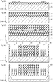
- FIGS. 1A to 1D are schematic diagrams illustrating a semiconductor device 100 according to a first embodiment.
- FIG. 1A is a top view schematically illustrating the semiconductor device 100 in the embodiment.
- the semiconductor device 100 is a scanner (optical scanner) formed by a MEMS technology.
- the optical scanner is used, for example, for scanning with light such as laser light.
- an x-axis, a y-axis intersecting the x-axis, and a z-axis intersecting the x-axis and the y-axis are defined.
- the term "intersecting" means "substantially intersecting".
- An x-direction being a direction parallel to the x-axis is an example of a first direction.
- a y-direction being a direction parallel to the y-axis is an example of a second direction.
- a z-direction being a direction parallel to the z-axis is an example of a third direction.
- a first actuator 2 has a rectangular shape and a long side 2a disposed to be parallel to the x-direction. As described later, a stage 20 is capable of pivoting on the y-axis by the first actuator 2.
- a second actuator 4 has a rectangular shape and a long side 4a disposed to be parallel to the x-direction. As described later, the stage 20 is capable of pivoting on the y-axis by the second actuator 4.
- the first actuator 2 is connected to a thirteenth connection member 96.
- the second actuator 4 is connected to a fourteenth connection member 98.
- the thirteenth connection member 96 and the fourteenth connection member 98 are connected to a substrate such as a silicon (Si) substrate, which is not illustrated in FIGS. 1A to 1D .
- the semiconductor device 100 is supported on the substrate (not illustrated in FIGS. 1A to 1D ).
- the thirteenth connection member 96 is provided in the vicinity of the middle of one end and the other end of the first actuator 2, to be adjacent to the first actuator 2.
- the fourteenth connection member 98 is provided in the vicinity of the middle of one end and the other end of the second actuator 4, to be adjacent to the second actuator 4.
- a first frame 6 is provided between the first actuator 2 and the second actuator 4.
- the first frame 6 is a frame-like member which is provided parallel to an xy plane and has a rectangular shape, for example. If the first frame 6 is provided parallel to the xy plane, a simple structure is obtained. Thus, this is preferable.
- One side of the first frame 6 is provided parallel to the x-axis, for example. Another side of the first frame 6 is provided parallel to the y-axis.
- the shape and the disposition of the first frame 6 are not limited to the embodiment.
- a first connection member 8 connects the first actuator 2 and the first frame 6 to each other.
- a second connection member 10 connects the first actuator 2 and the first frame 6 to each other at a position different from the position at which the first connection member 8 connects the first actuator 2 and the first frame 6 to each other. More specifically, one side of the first frame 6, which is illustrated on the left side in FIG. 1A and is parallel to the x-axis, is connected to one end of the first actuator 2 by the first connection member 8 and is connected to the other end of the first actuator 2 by the second connection member 10. Such connections allow a motion range of the scanner to increase, and thus are preferable.
- the first connection member 8 and the second connection member 10 are provided to be symmetrical with each other with respect to a plane parallel to a yz plane passing through the center of the thirteenth connection member 96.
- the first connection member 8 may not be connected to the one end of the first actuator 2
- the second connection member 10 may not be connected to the other end of the first actuator 2.
- a third connection member 12 connects the second actuator 4 and the first frame 6 to each other.
- a fourth connection member 14 connects the second actuator 4 and the first frame 6 to each other at a position different from the position at which the third connection member 12 connects the second actuator 4 and the first frame 6 to each other. More specifically, one side of the first frame 6, which is illustrated on the right side in FIG. 1A and is parallel to the x-axis, is connected to one end of the second actuator 4 by the third connection member 12 and is connected to the other end of the second actuator 4 by the fourth connection member 14. Such connections allow a motion range of the scanner to increase, and thus are preferable.
- the third connection member 12 and the fourth connection member 14 are provided to be symmetrical with each other with respect to a plane parallel to the yz plane passing through the center of the fourteenth connection member 98.
- the third connection member 12 may not be connected to the one end of the second actuator 4, and the fourth connection member 14 may not be connected to the other end of the second actuator 4.
- a third actuator 16 is provided on the inside of the first frame 6.
- the third actuator 16 has a rectangular shape and a long side 16a disposed to be parallel to the y-direction. As described later, the stage 20 is capable of pivoting on the x-axis by the third actuator 16.
- a fourth actuator 18 is provided on the inside of the first frame 6.
- the fourth actuator 18 has a rectangular shape and a long side 18a disposed to be parallel to the y-direction. As described later, the stage 20 is capable of pivoting on the x-axis by the fourth actuator 18.
- the stage 20 is provided between the third actuator 16 and the fourth actuator 18.
- the stage 20 includes, for example, a light reflector (mirror) 94 described later, and a device such as a vertical cavity surface emitting laser (VCSEL).
- a surface 20a of the stage 20 is parallel to the xy plane, for example.
- a fifth connection member 22 connects the third actuator 16 and the stage 20 to each other.
- a sixth connection member 24 connects the third actuator 16 and the stage 20 to each other at a position different from the position at which the fifth connection member 22 connects the third actuator 16 and the stage 20 to each other. More specifically, preferably, the stage 20 is connected to one end of the third actuator 16 by the fifth connection member 22 and is connected to the other end of the third actuator 16 by the sixth connection member 24.
- a seventh connection member 26 connects the fourth actuator 18 and the stage 20 to each other.
- An eighth connection member 28 connects the fourth actuator 18 and the stage 20 to each other at a position different from the position at which the seventh connection member 26 connects the fourth actuator 18 and the stage 20 to each other. More specifically, the stage 20 is connected to one end of the fourth actuator 18 by the seventh connection member 26 and is connected to the other end of the fourth actuator 18 by the eighth connection member 28.
- a ninth connection member 30 connects the third actuator 16 and the first frame 6 to each other.
- the ninth connection member 30 is provided in the vicinity of the middle of one end and the other end of the third actuator 16, to be adjacent to the third actuator 16, and connects the third actuator 16 and the first frame 6 to each other.
- the fifth connection member 22 and the sixth connection member 24 are provided to be symmetrical with each other with respect to a plane parallel to an xz plane passing through the center of the ninth connection member 30.
- the fifth connection member 22 may not be connected to the one end of the third actuator 16, and the sixth connection member 24 may not be connected to the other end of the third actuator 16.
- a tenth connection member 32 connects the fourth actuator 18 and the first frame 6 to each other.
- the tenth connection member 32 is provided in the vicinity of the middle of one end and the other end of the fourth actuator 18, to be adjacent to the fourth actuator 18, and connects the fourth actuator 18 and the first frame 6 to each other.
- the seventh connection member 26 and the eighth connection member 28 are provided to be symmetrical with each other with respect to a plane parallel to the xz plane passing through the center of the tenth connection member 32.
- the seventh connection member 26 may not be connected to the one end of the fourth actuator 18, and the eighth connection member 28 may not be connected to the other end of the fourth actuator 18.
- symmetry described in this specification may not have a meaning of completely corresponding to each other and may have a meaning of being shifted from each other by the degree of a manufacturing error.
- FIG. 1B is a sectional view schematically illustrating the semiconductor device 100 in the embodiment, in a section of A-A' in FIG. 1A.
- FIGS. 1C and 1D are sectional views illustrating enlarged sections of a sixth actuator 36 and an eighth actuator 40 in FIG. 1B .
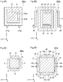
- FIGS. 2A and 2B are top views schematically illustrating the actuator and the surroundings of the actuator in the semiconductor device 100 in the embodiment.
- FIG. 2A is a top view schematically illustrating the structure of the first actuator 2 and the surroundings.
- FIG. 2B is a top view schematically illustrating the structure of the third actuator 16 and the surroundings.
- the first actuator 2 includes a fifth actuator 34 and the sixth actuator 36 which are provided to be adjacent to each other in the x-direction.
- the fifth actuator 34 is provided on the upper side of FIG. 1A .
- the sixth actuator 36 is provided on the lower side of FIG. 1A .
- the fifth actuator 34 is provided between the thirteenth connection member 96 and the first connection member 8.
- the sixth actuator 36 is provided between the thirteenth connection member 96 and the second connection member 10.
- the fifth actuator 34 includes a first metal layer 64a having a shape meandering in a plane parallel to the xy plane.
- the first metal layer 64a has a portion parallel to the x-direction.
- the portion of the first metal layer 64a, which is parallel to the x-direction is longer than the length of a portion of the first metal layer 64a, which is parallel to the y-direction.
- the sixth actuator 36 includes a first metal layer 64b.
- the first metal layer 64b has a shape meandering in a plane parallel to the xy plane and is not electrically connected to the first metal layer 64a.
- the first metal layer 64b has a portion parallel to the x-direction.
- the portion of the first metal layer 64b, which is parallel to the x-direction is longer than the length of a portion of the first metal layer 64b, which is parallel to the y-direction.
- the sixth actuator 36 includes a first oxide layer 60, a fourth oxide layer 70, and a first metal layer 64 which are sequentially stacked in the z-direction.
- the fourth oxide layer 70 is provided between the first oxide layer 60 and the first metal layer 64.
- the width of the fourth oxide layer 70 is narrower than the width of the first oxide layer 60.
- the section of the fifth actuator 34 also has a similar shape. Therefore, descriptions of the shape of the section of the fifth actuator 34 will not be repeated.
- a wiring (not illustrated) is connected to the first metal layer 64a.
- a wiring (not illustrated) different from the wiring connected to the first metal layer 64a is connected to the first metal layer 64b.
- a case where a current flows in the first metal layer 64b by using the above-described not-illustrated wiring is considered.
- heat is generated by Joule heat in the first metal layer 64b.
- the first metal layer 64b has a portion having a length in the x-direction, which is longer than a length in the y-direction. Therefore, the degree of thermal expansion by heat generation is larger in the x-direction larger than in the y-direction.
- the reason of the meandering shape is that an increase of resistance of a current flowing in the first metal layer 64b is desired in order to increase heat generated by Joule heat.
- the degree of thermal expansion of the first oxide layer 60 by heat generation is smaller than the degree of thermal expansion of the first metal layer 64b. Therefore, a portion of the sixth actuator 36, which is adjacent to the second connection member 10 in FIG. 1A , deforms to the back side of FIG. 1A by the heat generation. Thus, a portion of the first frame 6, which is connected to the second connection member 10, deforms to the back side of FIG. 1A . Thus, the tenth connection member 32, the fourth actuator 18, and the seventh connection member 26 deform. As a result, the lower left portion of the stage 20 in FIG. 1A deforms to the back side of FIG. 1A . As described later, the stage 20 is capable of pivoting on the y-axis by the sixth actuator 36. If the current does not flow in the first metal layer 64b, heat generation is suspended, and thus the shape is restored to the original shape.
- the first metal layer 64a has a portion having a length in the x-direction, which is longer than a length in the y-direction. Therefore, the degree of thermal expansion by heat generation is larger in the x-direction larger than in the y-direction.
- the degree of thermal expansion of the first oxide layer 60 by heat generation is smaller than the degree of thermal expansion of the first metal layer 64a. Therefore, a portion of the fifth actuator 34, which is adjacent to the first connection member 8 in FIG. 1A , deforms to the back side of FIG. 1A by the heat generation. Thus, a portion of the first frame 6, which is connected to the first connection member 8, deforms to the back side of FIG. 1A . Thus, the ninth connection member 30, the third actuator 16, and the fifth connection member 22 deform. As a result, the upper left portion of the stage 20 in FIG. 1A deforms to the back side of FIG. 1A . As described later, the stage 20 is capable of pivoting on the y-axis by the fifth actuator 34. If the current does not flow in the first metal layer 64a, heat generation is suspended, and thus the shape is restored to the original shape.
- the second actuator 4 includes a seventh actuator 38 and the eighth actuator 40 which are provided to be adjacent to each other in the x-direction.
- the seventh actuator 38 is provided on the upper side of FIG. 1A .
- the eighth actuator 40 is provided on the lower side of FIG. 1A .
- the seventh actuator 38 is provided between the fourteenth connection member 98 and the third connection member 12.
- the eighth actuator 40 is provided between the fourteenth connection member 98 and the fourth connection member 14.
- the shape of the seventh actuator 38 is similar to the shape of the fifth actuator 34.
- the shape of the eighth actuator 40 is similar to the shape of the sixth actuator 36.
- a case where a current flows in a first metal layer 64 of the seventh actuator 38 by using a wiring (not illustrated) connected to the first metal layer 64 of the seventh actuator 38 is considered. At this time, heat is generated by Joule heat in the first metal layer 64.
- the first metal layer 64 has a portion having a length in the x-direction, which is longer than a length in the y-direction. Therefore, the degree of thermal expansion by heat generation is larger in the x-direction larger than in the y-direction.
- the degree of thermal expansion of the first oxide layer 60 by heat generation is smaller than the degree of thermal expansion of the first metal layer 64. Therefore, a portion of the seventh actuator 38, which is adjacent to the third connection member 12 in FIG. 1A , deforms to the back side of FIG. 1A by the heat generation. Thus, a portion of the first frame 6, which is connected to the third connection member 12, deforms to the back side of FIG. 1A . Thus, the ninth connection member 30, the third actuator 16, and the sixth connection member 24 deform. As a result, the upper right portion of the stage 20 in FIG. 1A deforms to the back side of FIG. 1A . As described later, the stage 20 is capable of pivoting on the y-axis by the seventh actuator 38. If the current does not flow in the first metal layer 64, heat generation is suspended, and thus the shape is restored to the original shape.
- the first metal layer 64 has a portion having a length in the x-direction, which is longer than a length in the y-direction. Therefore, the degree of thermal expansion by heat generation is larger in the x-direction larger than in the y-direction.
- the degree of thermal expansion of the first oxide layer 60 by heat generation is smaller than the degree of thermal expansion of the first metal layer 64. Therefore, a portion of the eighth actuator 40, which is adjacent to the fourth connection member 14 in FIG. 1A , deforms to the back side of FIG. 1A by the heat generation. Thus, a portion of the first frame 6, which is connected to the fourth connection member 14, deforms to the back side of FIG. 1A . Thus, the tenth connection member 32, the fourth actuator 18, and the eighth connection member 28 deform. As a result, the lower right portion of the stage 20 in FIG. 1A deforms to the back side of FIG. 1A . As described later, the stage 20 is capable of pivoting on the y-axis by the eighth actuator 40. If the current does not flow in the first metal layer 64, heat generation is suspended, and thus the shape is restored to the original shape.
- the third actuator 16 includes a ninth actuator 42 and a tenth actuator 44 which are provided to be adjacent to each other in the y-direction.
- the ninth actuator 42 is provided on the left side of FIG. 1A .
- the tenth actuator 44 is provided on the right side of FIG. 1A .
- the ninth actuator 42 is provided between the ninth connection member 30 and the fifth connection member 22.
- the tenth actuator 44 is provided between the ninth connection member 30 and the sixth connection member 24.
- the ninth actuator 42 includes a first metal layer 64c having a shape meandering in a plane parallel to the xy plane.
- the first metal layer 64c has a portion parallel to the y-direction.
- the portion of the first metal layer 64c, which is parallel to the y-direction, is longer than the length of a portion of the first metal layer 64c, which is parallel to the x-direction.
- the tenth actuator 44 includes a first metal layer 64d.
- the first metal layer 64d has a shape meandering in a plane parallel to the xy plane and is not electrically connected to the first metal layer 64c.
- the first metal layer 64d has a portion parallel to the y-direction.
- the portion of the first metal layer 64d, which is parallel to the y-direction, is longer than the length of a portion of the first metal layer 64d, which is parallel to the x-direction.
- the sectional structure of the ninth actuator 42 and the sectional structure of the tenth actuator 44 are similar to the sectional structures of the fifth actuator 34, the sixth actuator 36, the seventh actuator 38, and the eighth actuator 40, and thus descriptions will not be repeated.
- a wiring (not illustrated) is connected to the first metal layer 64c.
- a wiring (not illustrated) different from the wiring connected to the first metal layer 64c is connected to the first metal layer 64d.
- a case where a current flows in the first metal layer 64c by using the above-described not-illustrated wiring is considered. At this time, heat is generated by Joule heat in the first metal layer 64c.
- the first metal layer 64c has a portion having a length in the y-direction, which is longer than a length in the x-direction. Therefore, the degree of thermal expansion by heat generation is larger in the y-direction larger than in the x-direction.
- the degree of thermal expansion of the first oxide layer 60 by heat generation is smaller than the degree of thermal expansion of the first metal layer 64c. Therefore, a portion of the ninth actuator 42, which is adjacent to the fifth connection member 22 in FIG. 1A , deforms to the back side of FIG. 1A by the heat generation. As a result, the upper left portion of the stage 20 in FIG. 1A deforms to the back side of FIG. 1A . As described later, the stage 20 is capable of pivoting on the x-axis by the ninth actuator 42. If the current does not flow in the first metal layer 64c, heat generation is suspended, and thus the shape is restored to the original shape.
- the first metal layer 64d has a portion having a length in the y-direction, which is longer than a length in the x-direction. Therefore, the degree of thermal expansion by heat generation is larger in the y-direction larger than in the x-direction.
- the degree of thermal expansion of the first oxide layer 60 by heat generation is smaller than the degree of thermal expansion of the first metal layer 64d. Therefore, a portion of the tenth actuator 44, which is adjacent to the sixth connection member 24 in FIG. 1A , deforms to the back side of FIG. 1A by the heat generation. As a result, the upper right portion of the stage 20 in FIG. 1A deforms to the back side of FIG. 1A . As described later, the stage 20 is capable of pivoting on the x-axis by the tenth actuator 44. If the current does not flow in the first metal layer 64d, heat generation is suspended, and thus the shape is restored to the original shape.
- the fourth actuator 18 includes an eleventh actuator 46 and the twelfth actuator 48 which are provided to be adjacent to each other in the y-direction.
- the eleventh actuator 46 is provided on the left side of FIG. 1A .
- the twelfth actuator 48 is provided on the right side of FIG. 1A .
- the eleventh actuator 46 is provided between the tenth connection member 32 and the seventh connection member 26.
- the twelfth actuator 48 is provided between the tenth connection member 32 and the eighth connection member 28.
- the shape of the eleventh actuator 46 is similar to the shape of the ninth actuator 42.
- the shape of the twelfth actuator 48 is similar to the shape of the tenth actuator 44.
- a case where a current flows in a first metal layer 64 of the eleventh actuator 46 by using a wiring (not illustrated) connected to the first metal layer 64 of the eleventh actuator is considered. At this time, heat is generated by Joule heat in the first metal layer 64.
- the first metal layer 64 has a portion having a length in the y-direction, which is longer than a length in the x-direction. Therefore, the degree of thermal expansion by heat generation is larger in the y-direction larger than in the x-direction.
- the degree of thermal expansion of the first oxide layer 60 by heat generation is smaller than the degree of thermal expansion of the first metal layer 64. Therefore, a portion of the eleventh actuator 46, which is adjacent to the seventh connection member 26 in FIG. 1A , deforms to the back side of FIG. 1A by the heat generation. As a result, the lower left portion of the stage 20 in FIG. 1A deforms to the back side of FIG. 1A . As described later, the stage 20 is capable of pivoting on the x-axis by the eleventh actuator 46. If the current does not flow in the first metal layer 64, heat generation is suspended, and thus the shape is restored to the original shape.
- the first metal layer 64 has a portion having a length in the y-direction, which is longer than a length in the x-direction. Therefore, the degree of thermal expansion by heat generation is larger in the y-direction larger than in the x-direction.
- the degree of thermal expansion of the first oxide layer 60 by heat generation is smaller than the degree of thermal expansion of the first metal layer 64. Therefore, a portion of the twelfth actuator 48, which is adjacent to the eighth connection member 28 in FIG. 1A , deforms to the back side of FIG. 1A by the heat generation. As a result, the lower right portion of the stage 20 in FIG. 1A deforms to the back side of FIG. 1A . As described later, the stage 20 is capable of pivoting on the x-axis by the twelfth actuator 48. If the current does not flow in the first metal layer 64, heat generation is suspended, and thus the shape is restored to the original shape.
- a plurality of first metal layers 64 is provided in sections of the first actuator 2 (fifth actuator 34 and sixth actuator 36) and the second actuator 4 (seventh actuator 38 and eighth actuator 40), which are parallel to the yz plane.
- the plurality of first metal layers 64 is stacked on the first oxide layer 60, with being arranged in the y-direction.
- the fourth oxide layer 70 is preferably provided between each of the plurality of first metal layers 64 and the first oxide layer 60.
- the fourth oxide layer 70 has a first portion 72a and a second portion 72b.
- the second portion 72b is provided between the first portion 72a and the first oxide layer 60 and has a width narrower than the width of the first portion 72a in the y-direction.
- the widths of the first portion 72a and the first oxide layer 60 in the y-direction may be equal to each other.
- the width of the first portion 72a in the y-direction may be narrower than the width of the first oxide layer 60 in the y-direction.
- each of the first frame 6 and the stage 20 includes a second oxide layer 62, a second metal layer 66, and a third oxide layer 68 which are sequentially stacked in the z-direction.
- the second metal layer 66 is interposed between the second oxide layer 62 and the third oxide layer 68. Therefore, even though there is an attempt of the second metal layer 66 expanding by heat generation, the second metal layer 66 is fixed by the second oxide layer 62 and the third oxide layer 68, and thus expansion is difficult.
- connection member 8 the second connection member 10
- third connection member 12 the fourth connection member 14
- fifth connection member 22 the sixth connection member 24
- seventh connection member 26 the eighth connection member 28
- ninth connection member 30 the tenth connection member 32
- second oxide layer 62 second metal layer 66
- third oxide layer 68 third oxide layer 68
- the semiconductor device 100 includes the first actuator 2, the second actuator 4, the first frame 6 provided between the first actuator 2 and the second actuator 4, the third actuator 16 provided on the inside of the first frame 6, the fourth actuator 18 provided on the inside of the first frame 6, and the stage 20 provided between the third actuator 16 and the fourth actuator 18.
- the stage 20 pivots by heat generated from the first actuator 2, the second actuator 4, the third actuator 16, or the fourth actuator 18, and a portion of the generated heat is transferred into the first frame 6.
- the portion of the generated heat, which has been transferred into the first frame 6 is transferred into the first actuator 2, the second actuator 4, the third actuator 16, or the fourth actuator 18 in which heat is not generated.
- the second metal layer 66 may have a simple layer shape as illustrated in FIG. 1B , which is different from the shape of the first metal layer 64 used in the actuator.
- the shape of the second metal layer 66 is not limited to the embodiment.
- the first oxide layer 60, the second oxide layer 62, the third oxide layer 68, and the fourth oxide layer 70 contain SiO x (silicon oxides), for example.
- SiO x silicon oxides
- SiO x is preferable because SiO x can be easily formed by oxidizing a portion of the substrate 90.
- the first metal layer 64 and the second metal layer 66 preferably contains Ag (silver), Cu (copper), Al (aluminum), and the like because of easy forming.
- Ag silver
- Cu copper
- Al aluminum
- the second metal layer 66 contains Al and the like, light such as laser light is reflected by the second metal layer 66. Therefore, the second metal layer 66 can be used as the light reflector (mirror) 94. For example, another light reflector may be formed on the stage 20.
- FIGS. 3A to 3E are sectional views schematically illustrating the semiconductor device in the middle of being manufactured, in a method of manufacturing the semiconductor device in the embodiment.
- An example using a Si substrate as the substrate 90 will be described below.
- an oxide layer 80 containing SiO x is formed on the substrate 90 by a local oxidation of silicon (LOCOS) method, for example.
- LOC local oxidation of silicon
- a stopper 88 containing polysilicon is formed on a portion of the oxide layer 80 ( FIG. 3A ). The stopper 88 is formed at a portion corresponding to the actuator in the semiconductor device 100.
- An oxide layer 82 being, for example, a tetraethoxysilane (TEOS) film or a borophosphosilicate glass (BPSG) film is formed on the oxide layer 80 and the stopper 88 ( FIG. 3B ).
- the oxide layer 80 and the oxide layer 82 constitute the first oxide layer 60, the second oxide layer 62, and the fourth oxide layer 70 in the semiconductor device 100.
- a metal layer 84 containing, for example, Al is formed on a portion of the oxide layer 82.
- the metal layer 84 is a metal layer to become the first metal layer 64 and the second metal layer 66.
- an oxide layer 86 being, for example, a TEOS film is formed on the oxide layer 82 and the metal layer 84.
- the surface of the oxide layer 86 is flattened, for example, by chemical mechanical polishing (CMP) ( FIG. 3C ).
- CMP chemical mechanical polishing
- portions of the oxide layer 80, the oxide layer 82, and the oxide layer 86 are removed, for example, by etching ( FIG. 3D ).
- the connection members first connection member 8, second connection member 10, third connection member 12, fourth connection member 14, fifth connection member 22, sixth connection member 24, seventh connection member 26, eighth connection member 28, ninth connection member 30, and tenth connection member 32
- the stopper 88 is provided at the portion corresponding to the actuator. Therefore, the oxide layer 80 disposed under the stopper 88 is not removed.
- the stopper 88 and a portion of the substrate 90 located under portions constituting the semiconductor device 100 are collectively removed, for example, by wet etching ( FIG. 3E ).
- the actuators first actuator 2, second actuator 4, third actuator 16, and fourth actuator 18
- both the substrate 90 and the stopper 88 have the same material.
- a vacuum space required for an electrostatic actuator or a magnet required for an electromagnetic actuator may not be used in a scanner using a thermal actuator. Thus, it is possible to reduce the size of the scanner.
- thermal separation means a method of conducting heat to a place to which heat is desired to be conducted in the scanner and of suppressing heat conduction to a place to which conduction of heat is not desired.
- the semiconductor device 100 includes the first frame 6. Therefore, thermal separation between heat applied to the actuator for driving around the x-axis and heat applied to the actuator for driving around the y-axis is performed well. Further, it is possible to keep balance between the heat applied to the actuator for driving around the x-axis and the heat applied to the actuator for driving around the y-axis. Therefore, it is possible to provide a semiconductor device (scanner) having a relatively simple structure, high controllability, and high performance.
- the first actuator 2 and the first frame 6 are connected to each other by the first connection member 8.
- the first actuator 2 and the first frame 6 are connected to each other by the second connection member 10 at a position different from the position at which the first connection member 8 connects the first actuator 2 and the first frame 6 to each other. Therefore, heat generated from the first actuator 2 is more evenly held by the first frame 6 in comparison to a case where the first actuator 2 and the first frame 6 are connected to each other at one position.
- a situation in which extra heat is transferred into the third actuator 16 and the fourth actuator 18 through the first frame 6 occurs less frequently. Therefore, it is possible to provide a semiconductor device (scanner) having a relatively simple structure, high controllability, and high performance.
- the second actuator 4 and the first frame 6 are connected to each other by the third connection member 12.
- the second actuator 4 and the first frame 6 are connected to each other by the fourth connection member 14 at a position different from the position at which the third connection member 12 connects the second actuator 4 and the first frame 6 to each other. Therefore, heat generated from the second actuator 4 is more evenly held by the first frame 6 in comparison to a case where the first actuator 2 and the first frame 6 are connected to each other at one position. As a result, a situation in which extra heat is transferred into the third actuator 16 and the fourth actuator 18 through the first frame 6 occurs less frequently. Therefore, it is possible to provide a semiconductor device (scanner) having a relatively simple structure, high controllability, and high performance.
- the third actuator 16 and the stage 20 are connected to each other by the fifth connection member 22.
- the third actuator 16 and the stage 20 are connected to each other by the sixth connection member 24 at a position different from the position at which the fifth connection member 22 connects the third actuator 16 and the stage 20 to each other.
- the fourth actuator 18 and the stage 20 are connected to each other by the seventh connection member 26.
- the fourth actuator 18 and the stage 20 are connected to each other by the eighth connection member 28 at a position different from the position at which the seventh connection member 26 connects the fourth actuator 18 and the stage 20 to each other.
- the thirteenth connection member 96 is provided in the vicinity of the middle of one end and the other end of the first actuator 2, to be adjacent to the first actuator 2.
- the fourteenth connection member 98 is provided in the vicinity of the middle of one end and the other end of the second actuator 4, to be adjacent to the second actuator 4.
- the ninth connection member 30 is provided in the vicinity of the middle of one end and the other end of the third actuator 16, to be adjacent to the third actuator 16, and connects the third actuator 16 and the first frame 6 to each other. Therefore, it is possible to secure both a distance of the first connection member 8, the first frame 6, and the ninth connection member 30 moving when heat of the first actuator 2 is transferred into the third actuator 16 and a distance of the third connection member 12, the first frame 6, and the ninth connection member 30 moving when heat of the second actuator 4 is transferred into the third actuator 16, to be long. Thus, a situation in which heat generated in the first actuator 2 and the second actuator 4 is transferred into the third actuator 16 occurs less frequently. Accordingly, it is possible to provide a semiconductor device (scanner) having a relatively simple structure and high controllability.
- the tenth connection member 32 is provided in the vicinity of the middle of one end and the other end of the fourth actuator 18, to be adjacent to the fourth actuator 18, and connects the fourth actuator 18 and the first frame 6 to each other. Therefore, it is possible to secure both a distance of the second connection member 10, the first frame 6, and the tenth connection member 32 moving when heat from the first actuator 2 is transferred into the fourth actuator 18 and a distance of the fourth connection member 14, the first frame 6, and the tenth connection member 32 moving when heat from the second actuator 4 is transferred into the fourth actuator 18, to be long. Thus, a situation in which heat generated in the first actuator 2 and the second actuator 4 is transferred into the fourth actuator 18 occurs less frequently. Accordingly, it is possible to provide a semiconductor device (scanner) having a relatively simple structure and high controllability.
- first connection member 8 connects the one end of the first actuator 2 to the first frame 6 and the second connection member 10 connects the other end of the first actuator 2 to the first frame 6, in other words, in a case where the ends of the actuator are connected to the first frame 6, it is possible to increase a range of the stage 20 deforming by the first actuator 2.
- connection member 12 connects the one end of the second actuator 4 to the first frame 6 and the fourth connection member 14 connects the other end of the second actuator 4 to the first frame 6, in other words, in a case where the ends of the actuator are connected to the first frame 6, it is possible to increase a range of the stage 20 deforming by the second actuator 4.
- connection member 22 connects the one end of the third actuator 16 to the stage 20
- sixth connection member 24 connects the other end of the third actuator 16 to the stage 20 in other words, in a case where the ends of the actuator are connected to the stage 20, it is possible to increase a range of the stage 20 deforming by the third actuator 16.
- connection member 26 connects the one end of the fourth actuator 18 to the stage 20
- eighth connection member 28 connects the other end of the fourth actuator 18 to the stage 20, in other words, in a case where the ends of the actuator are connected to the stage 20, it is possible to increase a range of the stage 20 deforming by the fourth actuator 18.
- the first connection member 8 and the second connection member 10 are provided to be symmetrical with each other with respect to an axis which is set to the plane parallel to the yz plane passing through the center of the thirteenth connection member 96. This is because heat transferred from the fifth actuator 34 into the first frame 6 through the first connection member 8 and a speed at which the heat is transferred are caused to be equal to heat transferred from the sixth actuator 36 into the first frame 6 through the second connection member 10 and a speed at which the heat is transferred, respectively.
- the third connection member 12 and the fourth connection member 14 are provided to be symmetrical with each other with respect to an axis set to the plane parallel to the yz plane passing through the center of the fourteenth connection member 98. This is because heat transferred from the seventh actuator 38 into the first frame 6 through the third connection member 12 and a speed at which the heat is transferred are caused to be equal to heat transferred from the eighth actuator 40 into the first frame 6 through the fourth connection member 14 and a speed at which the heat is transferred, respectively.
- the fifth connection member 22 and the sixth connection member 24 are provided to be symmetrical with each other with respect to an axis set to the plane parallel to the xz plane passing through the center of the ninth connection member 30. This is because heat transferred from the ninth actuator 42 into the stage 20 through the fifth connection member 22 and a speed at which the heat is transferred are caused to be equal to heat transferred from the tenth actuator 44 into the stage 20 through the sixth connection member 24 and a speed at which the heat is transferred, respectively.
- the seventh connection member 26 and the eighth connection member 28 are provided to be symmetrical with each other with respect to an axis set to the plane parallel to the xz plane passing through the center of the tenth connection member 32. This is because heat transferred from the eleventh actuator 46 into the stage 20 through the seventh connection member 26 and a speed at which the heat is transferred are caused to be equal to heat transferred from the twelfth actuator 48 into the stage 20 through the seventh connection member 26 and a speed at which the heat is transferred, respectively.
- Each of the first actuator 2, the second actuator 4, the third actuator 16, and the fourth actuator 18 includes the first oxide layer 60 and the first metal layer 64 sequentially stacked in the z-direction.
- a function as the actuator is obtained with a simple structure by expansion and contraction occurring by heat of the first metal layer 64.
- connection members first connection member 8, second connection member 10, third connection member 12, fourth connection member 14, fifth connection member 22, sixth connection member 24, seventh connection member 26, eighth connection member 28, ninth connection member 30, and tenth connection member 32
- the first frame 6, the stage 20, the thirteenth connection member 96, and the fourteenth connection member 98 includes the second oxide layer 62, the second metal layer 66, and the third oxide layer 68 sequentially stacked in the z-direction. Since expansion and contraction by heat of the second metal layer 66 are suppressed by the second oxide layer 62 and the third oxide layer 68, a structural body which has a simple structure and is thermally stable is obtained.
- FIGS. 5A and 5B are schematic diagrams illustrating an example of the section of the actuator in the semiconductor device 100 in the embodiment.
- FIG. 5A illustrates an example of the section of the actuator in the embodiment.
- FIG. 5B illustrates an example of a section of an actuator in a comparative form.
- the first oxide layer 60 may be integrally formed as illustrated in FIG. 5A rather than a case where the first oxide layer 60 is separated into oxide layers 60a, 60b, and 60c as illustrated in FIG. 5B .
- FIG. 5B if the oxide layers 60a, 60b, and 60c are individually pressed in the z-direction by the first metal layer 64, a distance of each of the oxide layers 60a, 60b, and 60c moving in the z-direction may vary. Thus, it is difficult to obtain a stable travel distance.
- FIG. 5A if the first oxide layer 60 is integrated, the entirety of the first oxide layer 60 is more stably pressed in the z-direction.
- the stopper 88 is provided, and the stopper 88 and the oxide layer 80 of the substrate 90 are set not to be removed.
- the fourth oxide layer 70 having a width narrower than the first oxide layer 60 is provided.
- the first portion 72a and the second portion 72b which is provided between the first portion 72a and the first oxide layer 60 and has a width narrower than the first portion 72a are provided in the fourth oxide layer 70.
- the first actuator 2 includes the fifth actuator 34 and the sixth actuator 36 provided to be adjacent to each other in the x-direction, it is possible to perform independent control, for example, for the operation of the stage 20, on the upper half side of the stage 20 and on the lower half side of the stage 20 in the drawings. Therefore, it is possible to control the stage 20 with higher precision.
- the second actuator 4 includes the seventh actuator 38 and the eighth actuator 40 provided to be adjacent to each other in the x-direction
- the third actuator 16 includes the ninth actuator 42 and the tenth actuator 44 provided to be adjacent to each other in the y-direction
- the fourth actuator 18 includes the eleventh actuator 46 and the twelfth actuator 48 provided to be adjacent to each other in the y-direction
- the first metal layer 64 and the second metal layer 66 particularly contain Al, and thus, processing is easy and a high thermal expansion coefficient is obtained. Accordingly, this is preferable.
- FIGS. 4A to 4D are schematic diagrams illustrating a semiconductor device in a comparison form of the embodiment.
- a semiconductor device 800a illustrated in FIG. 4A includes actuators 816a and 816b on the lower side of the first frame 6 in FIG. 4A .
- a stage 20 and actuators 802a and 802b are provided in the first frame 6.
- the actuators 802a and 802b are provided on the right side of the first frame 6 in FIG. 4A .
- the stage 20 pivots on the y-axis by the actuators 816a and 816b.
- the stage 20 pivots on the x-axis by the actuators 802a and 802b.
- the semiconductor device 800a in a case of applying heat to the actuator 816b, the heat is transferred into the actuator 802b through the first frame 6. Therefore, if the semiconductor device 800a is set to drive around the y-axis, the semiconductor device 800a also drives around the x-axis. Thus, there is a problem that an optical axis is shifted in an unintended direction.
- the first frame 6 is interposed between the first actuator 2 and the second actuator 4.
- the first actuator 2 and the second actuator 4 are connected to the first frame 6 by the first connection member 8 and the third connection member 12.
- the third actuator 16 and the fourth actuator 18 are provided between the first frame 6 and the stage 20.
- the third actuator 16 is connected to the first frame 6 by the ninth connection member 30 and is connected to the stage 20 by the fifth connection member 22.
- the fourth actuator 18 is connected to the first frame 6 by the tenth connection member 32 and is connected to the stage 20 by the seventh connection member 26.
- the stage 20 drives around the y-axis by the first actuator 2 and the second actuator 4.
- the stage 20 drives around the x-axis by the third actuator 16 and the fourth actuator 18.
- the first frame 6 is provided.
- heat separation between heat applied to the actuator for driving around the x-axis and heat applied to the actuator for driving around the y-axis is performed well, and it is possible to reduce the shift of the optical axis as shown in the semiconductor device 800a.
- the first connection member 8 and the third connection member 12 are provided on the upper side of FIG. 4B . Therefore, the heat applied to the first actuator 2 and the second actuator 4 is hardly conducted to the fourth actuator 18, but is conducted to the third actuator 16 well through the first frame 6 and the ninth connection member 30. Thus, there is a problem that the movement of the semiconductor device (scanner) becomes an asymmetric movement.
- a semiconductor device without the first frame 6 has a problem that heat conduction in the semiconductor device or the movement of the actuator by the heat conduction becomes complicated, and control as the semiconductor device (scanner) has difficulty.
- the semiconductor device in the embodiment it is possible to provide a high-performance semiconductor device.
- a semiconductor device 110 according to a second embodiment is different from the semiconductor device 100 in the first embodiment in that a second frame 50 is further provided on the inside of a first frame 6, and an eleventh connection member 52 and a twelfth connection member 54 connecting the first frame 6 and the second frame 50 to each other are provided.
- a second frame 50 is further provided on the inside of a first frame 6, and an eleventh connection member 52 and a twelfth connection member 54 connecting the first frame 6 and the second frame 50 to each other are provided.
- FIG. 6 is a schematic diagram illustrating the semiconductor device 110 in the embodiment.
- the second frame 50 is preferably provided parallel to a plane including the x-direction and the y-direction because of a simple structure. Since the second frame 50 is further provided, thermal separation between heat applied to the actuator for driving around the x-axis and heat applied to the actuator for driving around the y-axis is performed further better.
- the eleventh connection member 52 is provided in the vicinity of the middle of one end and the other end of a first actuator 2, to be adjacent to the first actuator 2, balance of heat which is generated from the first actuator 2 and is transferred into the second frame 50 through the first frame 6 is favorable. Thus, the heat is more evenly transferred into the second frame 50. Therefore, separation between heat generation in the first actuator 2 and heat generation in the third actuator 16 and the fourth actuator 18, which occurs by providing the first frame 6 and the second frame 50 is more accelerated.
- the semiconductor device in the embodiment it is possible to provide a high-performance semiconductor device.
- a semiconductor device is different from the semiconductor devices in the first and second embodiments in that first to fourth actuators are piezoelectric actuators.
- first to fourth actuators are piezoelectric actuators.
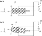
- FIGS. 7A and 7B are schematic diagram illustrating an example of an operation of the semiconductor device in the embodiment, in a case where a ninth actuator 42 is a piezoelectric actuator.
- the actuator includes a conductive plate 234, a first piezoelectric material 230, and a second piezoelectric material 232.
- the first piezoelectric material 230, and the second piezoelectric material 232 are provided to interpose the conductive plate 234.
- FIG. 7A illustrates a state where a switch 210 is in an off state. If the switch 210 turns into an on state, as in FIG. 7B , electric fields are applied to the first piezoelectric material 230 and the second piezoelectric material 232 from a power source 220.
- a direction of the electric field applied to the first piezoelectric material 230 is opposite to a direction of the electric field applied to the second piezoelectric material 232. Therefore, the entirety of the first piezoelectric material 230 and the second piezoelectric material 232 bends as illustrated in FIG. 7B .
- the first to fourth actuators are piezoelectric actuators, it is possible to provide a high-performance semiconductor device because two-axis control is possible with a simple structure.
Landscapes
- Physics & Mathematics (AREA)
- General Physics & Mathematics (AREA)
- Optics & Photonics (AREA)
- Engineering & Computer Science (AREA)
- Computer Hardware Design (AREA)
- Microelectronics & Electronic Packaging (AREA)
- Chemical & Material Sciences (AREA)
- Analytical Chemistry (AREA)
- Mechanical Light Control Or Optical Switches (AREA)
- Micromachines (AREA)
- Mechanical Optical Scanning Systems (AREA)
Abstract
Description
- Embodiments described herein relate generally to a semiconductor device.
- Micro electro mechanical systems (MEMS) which is a semiconductor device in which not only circuits but also microstructures, sensors, or mechanically-moving actuators are integrated can be formed by a microfabrication technology called as "micromachining", which is evolved from an integrated circuit technology. A high-performance actuator is required as an actuator to which the MEMS technology is applied.
-
-
FIGS. 1A to 1D are schematic diagrams illustrating a semiconductor device according to a first embodiment; -
FIGS. 2A and 2B are top views schematically illustrating an actuator and surroundings of the actuator in the semiconductor device in the first embodiment; -
FIGS. 3A to 3E are sectional views schematically illustrating the semiconductor device in the middle of being manufactured, in a method of manufacturing the semiconductor device in the first embodiment; -
FIGS. 4A to 4D are schematic diagrams illustrating a semiconductor device as a comparison form of the first embodiment; -
FIGS. 5A and 5B are schematic diagrams illustrating an example of a section of the actuator in the semiconductor device in the first embodiment; -
FIG. 6 is a schematic diagram illustrating a semiconductor device according to a second embodiment; and -
FIGS. 7A and 7B are schematic diagram illustrating an example of an operation of a piezoelectric actuator in a semiconductor device according to a third embodiment. - According to an embodiment, a semiconductor device includes a first actuator, a second actuator, a first frame provided between the first actuator and the second actuator, a first connection member connecting the first actuator and the first frame to each other, a second connection member connecting the first actuator and the first frame to each other at a position different from a position at which the first connection member connects the first actuator and the first frame to each other, a third connection member connecting the second actuator and the first frame to each other, a fourth connection member connecting the second actuator and the first frame to each other at a position different from a position at which the third connection member connects the second actuator and the first frame to each other, a third actuator provided on an inside of the first frame, a fourth actuator provided on the inside of the first frame, a stage provided between the third actuator and the fourth actuator, a fifth connection member connecting the third actuator and the stage to each other, a sixth connection member connecting the third actuator and the stage to each other at a position different from a position at which the fifth connection member connects the third actuator and the stage to each other, a seventh connection member connecting the fourth actuator and the stage to each other, an eighth connection member connecting the fourth actuator and the stage to each other at a position different from a position at which the seventh connection member connects the fourth actuator and the stage to each other, a ninth connection member connecting the third actuator and the first frame to each other, and a tenth connection member connecting the fourth actuator and the first frame to each other.
- Hereinafter, embodiments will be described with reference to the drawings. In the drawings, the same or similar parts are denoted by the same or similar reference signs.
-
FIGS. 1A to 1D are schematic diagrams illustrating asemiconductor device 100 according to a first embodiment. -
FIG. 1A is a top view schematically illustrating thesemiconductor device 100 in the embodiment. - In the embodiment, the
semiconductor device 100 is a scanner (optical scanner) formed by a MEMS technology. The optical scanner is used, for example, for scanning with light such as laser light. - Here, an x-axis, a y-axis intersecting the x-axis, and a z-axis intersecting the x-axis and the y-axis are defined. In the embodiment, the term "intersecting" means "substantially intersecting". An x-direction being a direction parallel to the x-axis is an example of a first direction. A y-direction being a direction parallel to the y-axis is an example of a second direction. A z-direction being a direction parallel to the z-axis is an example of a third direction.
- A
first actuator 2 has a rectangular shape and along side 2a disposed to be parallel to the x-direction. As described later, astage 20 is capable of pivoting on the y-axis by thefirst actuator 2. - A
second actuator 4 has a rectangular shape and along side 4a disposed to be parallel to the x-direction. As described later, thestage 20 is capable of pivoting on the y-axis by thesecond actuator 4. - The
first actuator 2 is connected to athirteenth connection member 96. Thesecond actuator 4 is connected to afourteenth connection member 98. For example, thethirteenth connection member 96 and thefourteenth connection member 98 are connected to a substrate such as a silicon (Si) substrate, which is not illustrated inFIGS. 1A to 1D . Thesemiconductor device 100 is supported on the substrate (not illustrated inFIGS. 1A to 1D ). Preferably, thethirteenth connection member 96 is provided in the vicinity of the middle of one end and the other end of thefirst actuator 2, to be adjacent to thefirst actuator 2. Preferably, thefourteenth connection member 98 is provided in the vicinity of the middle of one end and the other end of thesecond actuator 4, to be adjacent to thesecond actuator 4. - A
first frame 6 is provided between thefirst actuator 2 and thesecond actuator 4. Thefirst frame 6 is a frame-like member which is provided parallel to an xy plane and has a rectangular shape, for example. If thefirst frame 6 is provided parallel to the xy plane, a simple structure is obtained. Thus, this is preferable. One side of thefirst frame 6 is provided parallel to the x-axis, for example. Another side of thefirst frame 6 is provided parallel to the y-axis. The shape and the disposition of thefirst frame 6 are not limited to the embodiment. - A
first connection member 8 connects thefirst actuator 2 and thefirst frame 6 to each other. Asecond connection member 10 connects thefirst actuator 2 and thefirst frame 6 to each other at a position different from the position at which thefirst connection member 8 connects thefirst actuator 2 and thefirst frame 6 to each other. More specifically, one side of thefirst frame 6, which is illustrated on the left side inFIG. 1A and is parallel to the x-axis, is connected to one end of thefirst actuator 2 by thefirst connection member 8 and is connected to the other end of thefirst actuator 2 by thesecond connection member 10. Such connections allow a motion range of the scanner to increase, and thus are preferable. - Preferably, the
first connection member 8 and thesecond connection member 10 are provided to be symmetrical with each other with respect to a plane parallel to a yz plane passing through the center of thethirteenth connection member 96. In this case, thefirst connection member 8 may not be connected to the one end of thefirst actuator 2, and thesecond connection member 10 may not be connected to the other end of thefirst actuator 2. - A
third connection member 12 connects thesecond actuator 4 and thefirst frame 6 to each other. Afourth connection member 14 connects thesecond actuator 4 and thefirst frame 6 to each other at a position different from the position at which thethird connection member 12 connects thesecond actuator 4 and thefirst frame 6 to each other. More specifically, one side of thefirst frame 6, which is illustrated on the right side inFIG. 1A and is parallel to the x-axis, is connected to one end of thesecond actuator 4 by thethird connection member 12 and is connected to the other end of thesecond actuator 4 by thefourth connection member 14. Such connections allow a motion range of the scanner to increase, and thus are preferable. - Preferably, the
third connection member 12 and thefourth connection member 14 are provided to be symmetrical with each other with respect to a plane parallel to the yz plane passing through the center of thefourteenth connection member 98. In this case, thethird connection member 12 may not be connected to the one end of thesecond actuator 4, and thefourth connection member 14 may not be connected to the other end of thesecond actuator 4. - A
third actuator 16 is provided on the inside of thefirst frame 6. Thethird actuator 16 has a rectangular shape and along side 16a disposed to be parallel to the y-direction. As described later, thestage 20 is capable of pivoting on the x-axis by thethird actuator 16. - A
fourth actuator 18 is provided on the inside of thefirst frame 6. Thefourth actuator 18 has a rectangular shape and along side 18a disposed to be parallel to the y-direction. As described later, thestage 20 is capable of pivoting on the x-axis by thefourth actuator 18. - The
stage 20 is provided between thethird actuator 16 and thefourth actuator 18. Thestage 20 includes, for example, a light reflector (mirror) 94 described later, and a device such as a vertical cavity surface emitting laser (VCSEL). Asurface 20a of thestage 20 is parallel to the xy plane, for example. - A
fifth connection member 22 connects thethird actuator 16 and thestage 20 to each other. Asixth connection member 24 connects thethird actuator 16 and thestage 20 to each other at a position different from the position at which thefifth connection member 22 connects thethird actuator 16 and thestage 20 to each other. More specifically, preferably, thestage 20 is connected to one end of thethird actuator 16 by thefifth connection member 22 and is connected to the other end of thethird actuator 16 by thesixth connection member 24. - A
seventh connection member 26 connects thefourth actuator 18 and thestage 20 to each other. Aneighth connection member 28 connects thefourth actuator 18 and thestage 20 to each other at a position different from the position at which theseventh connection member 26 connects thefourth actuator 18 and thestage 20 to each other. More specifically, thestage 20 is connected to one end of thefourth actuator 18 by theseventh connection member 26 and is connected to the other end of thefourth actuator 18 by theeighth connection member 28. - A
ninth connection member 30 connects thethird actuator 16 and thefirst frame 6 to each other. Preferably, theninth connection member 30 is provided in the vicinity of the middle of one end and the other end of thethird actuator 16, to be adjacent to thethird actuator 16, and connects thethird actuator 16 and thefirst frame 6 to each other. - Preferably, the
fifth connection member 22 and thesixth connection member 24 are provided to be symmetrical with each other with respect to a plane parallel to an xz plane passing through the center of theninth connection member 30. In this case, thefifth connection member 22 may not be connected to the one end of thethird actuator 16, and thesixth connection member 24 may not be connected to the other end of thethird actuator 16. - A
tenth connection member 32 connects thefourth actuator 18 and thefirst frame 6 to each other. Preferably, thetenth connection member 32 is provided in the vicinity of the middle of one end and the other end of thefourth actuator 18, to be adjacent to thefourth actuator 18, and connects thefourth actuator 18 and thefirst frame 6 to each other. - Preferably, the
seventh connection member 26 and theeighth connection member 28 are provided to be symmetrical with each other with respect to a plane parallel to the xz plane passing through the center of thetenth connection member 32. In this case, theseventh connection member 26 may not be connected to the one end of thefourth actuator 18, and theeighth connection member 28 may not be connected to the other end of thefourth actuator 18. - The term "symmetry" described in this specification may not have a meaning of completely corresponding to each other and may have a meaning of being shifted from each other by the degree of a manufacturing error.
-
FIG. 1B is a sectional view schematically illustrating thesemiconductor device 100 in the embodiment, in a section of A-A' inFIG. 1A. FIGS. 1C and 1D are sectional views illustrating enlarged sections of asixth actuator 36 and aneighth actuator 40 inFIG. 1B . -
FIGS. 2A and 2B are top views schematically illustrating the actuator and the surroundings of the actuator in thesemiconductor device 100 in the embodiment.FIG. 2A is a top view schematically illustrating the structure of thefirst actuator 2 and the surroundings.FIG. 2B is a top view schematically illustrating the structure of thethird actuator 16 and the surroundings. - The structure of the actuator in the embodiment will be described with reference to
FIGS. 1B to 1D ,2A, and 2B . - The
first actuator 2 includes afifth actuator 34 and thesixth actuator 36 which are provided to be adjacent to each other in the x-direction. Thefifth actuator 34 is provided on the upper side ofFIG. 1A . Thesixth actuator 36 is provided on the lower side ofFIG. 1A . For example, thefifth actuator 34 is provided between thethirteenth connection member 96 and thefirst connection member 8. Thesixth actuator 36 is provided between thethirteenth connection member 96 and thesecond connection member 10. - For example, as illustrated in
FIG. 2A , thefifth actuator 34 includes afirst metal layer 64a having a shape meandering in a plane parallel to the xy plane. Thefirst metal layer 64a has a portion parallel to the x-direction. The portion of thefirst metal layer 64a, which is parallel to the x-direction, is longer than the length of a portion of thefirst metal layer 64a, which is parallel to the y-direction. Thesixth actuator 36 includes afirst metal layer 64b. Thefirst metal layer 64b has a shape meandering in a plane parallel to the xy plane and is not electrically connected to thefirst metal layer 64a. Thefirst metal layer 64b has a portion parallel to the x-direction. The portion of thefirst metal layer 64b, which is parallel to the x-direction, is longer than the length of a portion of thefirst metal layer 64b, which is parallel to the y-direction. - For example, as illustrated in
FIG. 1C , in the section of A-A' inFIG. 1A , thesixth actuator 36 includes afirst oxide layer 60, afourth oxide layer 70, and afirst metal layer 64 which are sequentially stacked in the z-direction. In other words, thefourth oxide layer 70 is provided between thefirst oxide layer 60 and thefirst metal layer 64. The width of thefourth oxide layer 70 is narrower than the width of thefirst oxide layer 60. The section of thefifth actuator 34 also has a similar shape. Therefore, descriptions of the shape of the section of thefifth actuator 34 will not be repeated. - For example, a wiring (not illustrated) is connected to the
first metal layer 64a. For example, a wiring (not illustrated) different from the wiring connected to thefirst metal layer 64a is connected to thefirst metal layer 64b. - A case where a current flows in the
first metal layer 64b by using the above-described not-illustrated wiring is considered. At this time, heat is generated by Joule heat in thefirst metal layer 64b. Here, as described above, thefirst metal layer 64b has a portion having a length in the x-direction, which is longer than a length in the y-direction. Therefore, the degree of thermal expansion by heat generation is larger in the x-direction larger than in the y-direction. The reason of the meandering shape is that an increase of resistance of a current flowing in thefirst metal layer 64b is desired in order to increase heat generated by Joule heat. - The degree of thermal expansion of the
first oxide layer 60 by heat generation is smaller than the degree of thermal expansion of thefirst metal layer 64b. Therefore, a portion of thesixth actuator 36, which is adjacent to thesecond connection member 10 inFIG. 1A , deforms to the back side ofFIG. 1A by the heat generation. Thus, a portion of thefirst frame 6, which is connected to thesecond connection member 10, deforms to the back side ofFIG. 1A . Thus, thetenth connection member 32, thefourth actuator 18, and theseventh connection member 26 deform. As a result, the lower left portion of thestage 20 inFIG. 1A deforms to the back side ofFIG. 1A . As described later, thestage 20 is capable of pivoting on the y-axis by thesixth actuator 36. If the current does not flow in thefirst metal layer 64b, heat generation is suspended, and thus the shape is restored to the original shape. - Next, a case where a current flows in the
first metal layer 64a is considered. At this time, heat is generated by Joule heat in thefirst metal layer 64a. Here, as described above, thefirst metal layer 64a has a portion having a length in the x-direction, which is longer than a length in the y-direction. Therefore, the degree of thermal expansion by heat generation is larger in the x-direction larger than in the y-direction. - The degree of thermal expansion of the
first oxide layer 60 by heat generation is smaller than the degree of thermal expansion of thefirst metal layer 64a. Therefore, a portion of thefifth actuator 34, which is adjacent to thefirst connection member 8 inFIG. 1A , deforms to the back side ofFIG. 1A by the heat generation. Thus, a portion of thefirst frame 6, which is connected to thefirst connection member 8, deforms to the back side ofFIG. 1A . Thus, theninth connection member 30, thethird actuator 16, and thefifth connection member 22 deform. As a result, the upper left portion of thestage 20 inFIG. 1A deforms to the back side ofFIG. 1A . As described later, thestage 20 is capable of pivoting on the y-axis by thefifth actuator 34. If the current does not flow in thefirst metal layer 64a, heat generation is suspended, and thus the shape is restored to the original shape. - The
second actuator 4 includes aseventh actuator 38 and theeighth actuator 40 which are provided to be adjacent to each other in the x-direction. Theseventh actuator 38 is provided on the upper side ofFIG. 1A . Theeighth actuator 40 is provided on the lower side ofFIG. 1A . For example, theseventh actuator 38 is provided between thefourteenth connection member 98 and thethird connection member 12. Theeighth actuator 40 is provided between thefourteenth connection member 98 and thefourth connection member 14. - For example, the shape of the
seventh actuator 38 is similar to the shape of thefifth actuator 34. The shape of theeighth actuator 40 is similar to the shape of thesixth actuator 36. - A case where a current flows in a
first metal layer 64 of theseventh actuator 38 by using a wiring (not illustrated) connected to thefirst metal layer 64 of theseventh actuator 38 is considered. At this time, heat is generated by Joule heat in thefirst metal layer 64. Here, as described above, thefirst metal layer 64 has a portion having a length in the x-direction, which is longer than a length in the y-direction. Therefore, the degree of thermal expansion by heat generation is larger in the x-direction larger than in the y-direction. - The degree of thermal expansion of the
first oxide layer 60 by heat generation is smaller than the degree of thermal expansion of thefirst metal layer 64. Therefore, a portion of theseventh actuator 38, which is adjacent to thethird connection member 12 inFIG. 1A , deforms to the back side ofFIG. 1A by the heat generation. Thus, a portion of thefirst frame 6, which is connected to thethird connection member 12, deforms to the back side ofFIG. 1A . Thus, theninth connection member 30, thethird actuator 16, and thesixth connection member 24 deform. As a result, the upper right portion of thestage 20 inFIG. 1A deforms to the back side ofFIG. 1A . As described later, thestage 20 is capable of pivoting on the y-axis by theseventh actuator 38. If the current does not flow in thefirst metal layer 64, heat generation is suspended, and thus the shape is restored to the original shape. - Next, a case where a current flows in a
first metal layer 64 of theeighth actuator 40 by using a wiring (not illustrated) connected to thefirst metal layer 64 of theeighth actuator 40 is considered. At this time, heat is generated by Joule heat in thefirst metal layer 64. Here, as described above, thefirst metal layer 64 has a portion having a length in the x-direction, which is longer than a length in the y-direction. Therefore, the degree of thermal expansion by heat generation is larger in the x-direction larger than in the y-direction. - The degree of thermal expansion of the
first oxide layer 60 by heat generation is smaller than the degree of thermal expansion of thefirst metal layer 64. Therefore, a portion of theeighth actuator 40, which is adjacent to thefourth connection member 14 inFIG. 1A , deforms to the back side ofFIG. 1A by the heat generation. Thus, a portion of thefirst frame 6, which is connected to thefourth connection member 14, deforms to the back side ofFIG. 1A . Thus, thetenth connection member 32, thefourth actuator 18, and theeighth connection member 28 deform. As a result, the lower right portion of thestage 20 inFIG. 1A deforms to the back side ofFIG. 1A . As described later, thestage 20 is capable of pivoting on the y-axis by theeighth actuator 40. If the current does not flow in thefirst metal layer 64, heat generation is suspended, and thus the shape is restored to the original shape. - The
third actuator 16 includes aninth actuator 42 and atenth actuator 44 which are provided to be adjacent to each other in the y-direction. Theninth actuator 42 is provided on the left side ofFIG. 1A . Thetenth actuator 44 is provided on the right side ofFIG. 1A . For example, theninth actuator 42 is provided between theninth connection member 30 and thefifth connection member 22. Thetenth actuator 44 is provided between theninth connection member 30 and thesixth connection member 24. - For example, as illustrated in
FIG. 2B , theninth actuator 42 includes afirst metal layer 64c having a shape meandering in a plane parallel to the xy plane. Thefirst metal layer 64c has a portion parallel to the y-direction. The portion of thefirst metal layer 64c, which is parallel to the y-direction, is longer than the length of a portion of thefirst metal layer 64c, which is parallel to the x-direction. Thetenth actuator 44 includes afirst metal layer 64d. Thefirst metal layer 64d has a shape meandering in a plane parallel to the xy plane and is not electrically connected to thefirst metal layer 64c. Thefirst metal layer 64d has a portion parallel to the y-direction. The portion of thefirst metal layer 64d, which is parallel to the y-direction, is longer than the length of a portion of thefirst metal layer 64d, which is parallel to the x-direction. The sectional structure of theninth actuator 42 and the sectional structure of thetenth actuator 44 are similar to the sectional structures of thefifth actuator 34, thesixth actuator 36, theseventh actuator 38, and theeighth actuator 40, and thus descriptions will not be repeated. - For example, a wiring (not illustrated) is connected to the
first metal layer 64c. For example, a wiring (not illustrated) different from the wiring connected to thefirst metal layer 64c is connected to thefirst metal layer 64d. - A case where a current flows in the
first metal layer 64c by using the above-described not-illustrated wiring is considered. At this time, heat is generated by Joule heat in thefirst metal layer 64c. Here, as described above, thefirst metal layer 64c has a portion having a length in the y-direction, which is longer than a length in the x-direction. Therefore, the degree of thermal expansion by heat generation is larger in the y-direction larger than in the x-direction. - The degree of thermal expansion of the
first oxide layer 60 by heat generation is smaller than the degree of thermal expansion of thefirst metal layer 64c. Therefore, a portion of theninth actuator 42, which is adjacent to thefifth connection member 22 inFIG. 1A , deforms to the back side ofFIG. 1A by the heat generation. As a result, the upper left portion of thestage 20 inFIG. 1A deforms to the back side ofFIG. 1A . As described later, thestage 20 is capable of pivoting on the x-axis by theninth actuator 42. If the current does not flow in thefirst metal layer 64c, heat generation is suspended, and thus the shape is restored to the original shape. - Next, a case where a current flows in the
first metal layer 64d is considered. At this time, heat is generated by Joule heat in thefirst metal layer 64d. Here, as described above, thefirst metal layer 64d has a portion having a length in the y-direction, which is longer than a length in the x-direction. Therefore, the degree of thermal expansion by heat generation is larger in the y-direction larger than in the x-direction. - The degree of thermal expansion of the
first oxide layer 60 by heat generation is smaller than the degree of thermal expansion of thefirst metal layer 64d. Therefore, a portion of thetenth actuator 44, which is adjacent to thesixth connection member 24 inFIG. 1A , deforms to the back side ofFIG. 1A by the heat generation. As a result, the upper right portion of thestage 20 inFIG. 1A deforms to the back side ofFIG. 1A . As described later, thestage 20 is capable of pivoting on the x-axis by thetenth actuator 44. If the current does not flow in thefirst metal layer 64d, heat generation is suspended, and thus the shape is restored to the original shape. - The
fourth actuator 18 includes aneleventh actuator 46 and thetwelfth actuator 48 which are provided to be adjacent to each other in the y-direction. Theeleventh actuator 46 is provided on the left side ofFIG. 1A . Thetwelfth actuator 48 is provided on the right side ofFIG. 1A . For example, theeleventh actuator 46 is provided between thetenth connection member 32 and theseventh connection member 26. Thetwelfth actuator 48 is provided between thetenth connection member 32 and theeighth connection member 28. - For example, the shape of the
eleventh actuator 46 is similar to the shape of theninth actuator 42. The shape of thetwelfth actuator 48 is similar to the shape of thetenth actuator 44. - A case where a current flows in a
first metal layer 64 of theeleventh actuator 46 by using a wiring (not illustrated) connected to thefirst metal layer 64 of the eleventh actuator is considered. At this time, heat is generated by Joule heat in thefirst metal layer 64. Here, as described above, thefirst metal layer 64 has a portion having a length in the y-direction, which is longer than a length in the x-direction. Therefore, the degree of thermal expansion by heat generation is larger in the y-direction larger than in the x-direction. - The degree of thermal expansion of the
first oxide layer 60 by heat generation is smaller than the degree of thermal expansion of thefirst metal layer 64. Therefore, a portion of theeleventh actuator 46, which is adjacent to theseventh connection member 26 inFIG. 1A , deforms to the back side ofFIG. 1A by the heat generation. As a result, the lower left portion of thestage 20 inFIG. 1A deforms to the back side ofFIG. 1A . As described later, thestage 20 is capable of pivoting on the x-axis by theeleventh actuator 46. If the current does not flow in thefirst metal layer 64, heat generation is suspended, and thus the shape is restored to the original shape. - Next, a case where a current flows in a
first metal layer 64 of thetwelfth actuator 48 by using a wiring (not illustrated) connected to thefirst metal layer 64 of thetwelfth actuator 48 is considered. At this time, heat is generated by Joule heat in thefirst metal layer 64. Here, as described above, thefirst metal layer 64 has a portion having a length in the y-direction, which is longer than a length in the x-direction. Therefore, the degree of thermal expansion by heat generation is larger in the y-direction larger than in the x-direction. - The degree of thermal expansion of the
first oxide layer 60 by heat generation is smaller than the degree of thermal expansion of thefirst metal layer 64. Therefore, a portion of thetwelfth actuator 48, which is adjacent to theeighth connection member 28 inFIG. 1A , deforms to the back side ofFIG. 1A by the heat generation. As a result, the lower right portion of thestage 20 inFIG. 1A deforms to the back side ofFIG. 1A . As described later, thestage 20 is capable of pivoting on the x-axis by thetwelfth actuator 48. If the current does not flow in thefirst metal layer 64, heat generation is suspended, and thus the shape is restored to the original shape. - Preferably, a plurality of first metal layers 64 is provided in sections of the first actuator 2 (
fifth actuator 34 and sixth actuator 36) and the second actuator 4 (seventh actuator 38 and eighth actuator 40), which are parallel to the yz plane. Preferably, the plurality of first metal layers 64 is stacked on thefirst oxide layer 60, with being arranged in the y-direction. Thefourth oxide layer 70 is preferably provided between each of the plurality offirst metal layers 64 and thefirst oxide layer 60. Preferably, thefourth oxide layer 70 has afirst portion 72a and asecond portion 72b. Thesecond portion 72b is provided between thefirst portion 72a and thefirst oxide layer 60 and has a width narrower than the width of thefirst portion 72a in the y-direction. For example, the widths of thefirst portion 72a and thefirst oxide layer 60 in the y-direction may be equal to each other. For example, the width of thefirst portion 72a in the y-direction may be narrower than the width of thefirst oxide layer 60 in the y-direction. The above descriptions are similarly applied to the third actuator 16 (ninth actuator 42 and tenth actuator 44) and the fourth actuator 18 (eleventh actuator 46 and twelfth actuator 48). - As illustrated in
FIG. 1B , each of thefirst frame 6 and thestage 20 includes asecond oxide layer 62, asecond metal layer 66, and athird oxide layer 68 which are sequentially stacked in the z-direction. In other words, thesecond metal layer 66 is interposed between thesecond oxide layer 62 and thethird oxide layer 68. Therefore, even though there is an attempt of thesecond metal layer 66 expanding by heat generation, thesecond metal layer 66 is fixed by thesecond oxide layer 62 and thethird oxide layer 68, and thus expansion is difficult. Similarly, thefirst connection member 8, thesecond connection member 10, thethird connection member 12, thefourth connection member 14, thefifth connection member 22, thesixth connection member 24, theseventh connection member 26, theeighth connection member 28, theninth connection member 30, and thetenth connection member 32 have the similar stacked structure (second oxide layer 62,second metal layer 66, and the third oxide layer 68), and thus have difficulty in expanding by heat generation. - As a result, only the actuator deforms largely by applying heat, and thus the
stage 20 deforms. - In other words, in the embodiment, the
semiconductor device 100 includes thefirst actuator 2, thesecond actuator 4, thefirst frame 6 provided between thefirst actuator 2 and thesecond actuator 4, thethird actuator 16 provided on the inside of thefirst frame 6, thefourth actuator 18 provided on the inside of thefirst frame 6, and thestage 20 provided between thethird actuator 16 and thefourth actuator 18. Thestage 20 pivots by heat generated from thefirst actuator 2, thesecond actuator 4, thethird actuator 16, or thefourth actuator 18, and a portion of the generated heat is transferred into thefirst frame 6. The portion of the generated heat, which has been transferred into thefirst frame 6 is transferred into thefirst actuator 2, thesecond actuator 4, thethird actuator 16, or thefourth actuator 18 in which heat is not generated. - As described above, regarding the shape of the
second metal layer 66, control of expansion and contraction by thermal expansion is not required. Therefore, for easy manufacturing, thesecond metal layer 66 may have a simple layer shape as illustrated inFIG. 1B , which is different from the shape of thefirst metal layer 64 used in the actuator. The shape of thesecond metal layer 66 is not limited to the embodiment. - The
first oxide layer 60, thesecond oxide layer 62, thethird oxide layer 68, and thefourth oxide layer 70 contain SiOx (silicon oxides), for example. In particular, in a case of using a Si substrate as asubstrate 90, SiOx is preferable because SiOx can be easily formed by oxidizing a portion of thesubstrate 90. - The
first metal layer 64 and thesecond metal layer 66 preferably contains Ag (silver), Cu (copper), Al (aluminum), and the like because of easy forming. In particular, in a case of containing Al, it is easy to form a metal layer of Al on a Si substrate as thesubstrate 90. Thus, this case is preferable. - For example, in a case where the
second metal layer 66 contains Al and the like, light such as laser light is reflected by thesecond metal layer 66. Therefore, thesecond metal layer 66 can be used as the light reflector (mirror) 94. For example, another light reflector may be formed on thestage 20. -
FIGS. 3A to 3E are sectional views schematically illustrating the semiconductor device in the middle of being manufactured, in a method of manufacturing the semiconductor device in the embodiment. An example using a Si substrate as thesubstrate 90 will be described below. - Firstly, an
oxide layer 80 containing SiOx is formed on thesubstrate 90 by a local oxidation of silicon (LOCOS) method, for example. Then, for example, astopper 88 containing polysilicon is formed on a portion of the oxide layer 80 (FIG. 3A ). Thestopper 88 is formed at a portion corresponding to the actuator in thesemiconductor device 100. - An
oxide layer 82 being, for example, a tetraethoxysilane (TEOS) film or a borophosphosilicate glass (BPSG) film is formed on theoxide layer 80 and the stopper 88 (FIG. 3B ). Theoxide layer 80 and theoxide layer 82 constitute thefirst oxide layer 60, thesecond oxide layer 62, and thefourth oxide layer 70 in thesemiconductor device 100. - Then, a
metal layer 84 containing, for example, Al is formed on a portion of theoxide layer 82. Themetal layer 84 is a metal layer to become thefirst metal layer 64 and thesecond metal layer 66. Then, anoxide layer 86 being, for example, a TEOS film is formed on theoxide layer 82 and themetal layer 84. The surface of theoxide layer 86 is flattened, for example, by chemical mechanical polishing (CMP) (FIG. 3C ). Theoxide layer 86 constitutes thethird oxide layer 68 in thesemiconductor device 100. - Then, portions of the
oxide layer 80, theoxide layer 82, and theoxide layer 86 are removed, for example, by etching (FIG. 3D ). Thus, the connection members (first connection member 8,second connection member 10,third connection member 12,fourth connection member 14,fifth connection member 22,sixth connection member 24,seventh connection member 26,eighth connection member 28,ninth connection member 30, and tenth connection member 32), thefirst frame 6, thestage 20, thethirteenth connection member 96, and thefourteenth connection member 98 are formed. Thestopper 88 is provided at the portion corresponding to the actuator. Therefore, theoxide layer 80 disposed under thestopper 88 is not removed. - Then, the
stopper 88 and a portion of thesubstrate 90 located under portions constituting thesemiconductor device 100 are collectively removed, for example, by wet etching (FIG. 3E ). Thus, the actuators (first actuator 2,second actuator 4,third actuator 16, and fourth actuator 18) are formed. Here, in a case where thesubstrate 90 is a Si substrate, and thestopper 88 contains polysilicon, both thesubstrate 90 and thestopper 88 have the same material. Thus, it is possible to remove thesubstrate 90 and thestopper 88 in the similar process. In this manner, thesemiconductor device 100 in the embodiment is obtained. - Next, effects of the
semiconductor device 100 in the embodiment will be described. - With the semiconductor device in the embodiment, it is possible to provide a high-performance semiconductor device.
- A vacuum space required for an electrostatic actuator or a magnet required for an electromagnetic actuator may not be used in a scanner using a thermal actuator. Thus, it is possible to reduce the size of the scanner.
- Since heat conduction in the scanner takes time, securing an operation speed of the scanner may act as a problem. However, the scanner manufactured by the MEMS technology is naturally small. Thus, heat is conducted in the scanner in a short time. Therefore, the problem in the operation speed occurs less frequently.
- In a case using the thermal actuator in the scanner, a method of performing thermal separation in the scanner becomes a problem. Here, thermal separation means a method of conducting heat to a place to which heat is desired to be conducted in the scanner and of suppressing heat conduction to a place to which conduction of heat is not desired.
- In the embodiment, the
semiconductor device 100 includes thefirst frame 6. Therefore, thermal separation between heat applied to the actuator for driving around the x-axis and heat applied to the actuator for driving around the y-axis is performed well. Further, it is possible to keep balance between the heat applied to the actuator for driving around the x-axis and the heat applied to the actuator for driving around the y-axis. Therefore, it is possible to provide a semiconductor device (scanner) having a relatively simple structure, high controllability, and high performance. - The
first actuator 2 and thefirst frame 6 are connected to each other by thefirst connection member 8. Thefirst actuator 2 and thefirst frame 6 are connected to each other by thesecond connection member 10 at a position different from the position at which thefirst connection member 8 connects thefirst actuator 2 and thefirst frame 6 to each other. Therefore, heat generated from thefirst actuator 2 is more evenly held by thefirst frame 6 in comparison to a case where thefirst actuator 2 and thefirst frame 6 are connected to each other at one position. As a result, a situation in which extra heat is transferred into thethird actuator 16 and thefourth actuator 18 through thefirst frame 6 occurs less frequently. Therefore, it is possible to provide a semiconductor device (scanner) having a relatively simple structure, high controllability, and high performance. - The
second actuator 4 and thefirst frame 6 are connected to each other by thethird connection member 12. Thesecond actuator 4 and thefirst frame 6 are connected to each other by thefourth connection member 14 at a position different from the position at which thethird connection member 12 connects thesecond actuator 4 and thefirst frame 6 to each other. Therefore, heat generated from thesecond actuator 4 is more evenly held by thefirst frame 6 in comparison to a case where thefirst actuator 2 and thefirst frame 6 are connected to each other at one position. As a result, a situation in which extra heat is transferred into thethird actuator 16 and thefourth actuator 18 through thefirst frame 6 occurs less frequently. Therefore, it is possible to provide a semiconductor device (scanner) having a relatively simple structure, high controllability, and high performance. - The
third actuator 16 and thestage 20 are connected to each other by thefifth connection member 22. Thethird actuator 16 and thestage 20 are connected to each other by thesixth connection member 24 at a position different from the position at which thefifth connection member 22 connects thethird actuator 16 and thestage 20 to each other. Thus, it is easy to more evenly transfer heat generated from thethird actuator 16 into thestage 20. Therefore, a situation in which extra heat is transferred into thefirst actuator 2 and thesecond actuator 4 through thefirst frame 6 occurs less frequently in comparison to a case where thethird actuator 16 and thestage 20 are connected at one position. Therefore, it is possible to provide a semiconductor device (scanner) having a relatively simple structure and high controllability. - The
fourth actuator 18 and thestage 20 are connected to each other by theseventh connection member 26. Thefourth actuator 18 and thestage 20 are connected to each other by theeighth connection member 28 at a position different from the position at which theseventh connection member 26 connects thefourth actuator 18 and thestage 20 to each other. Thus, it is easy to more evenly transfer heat generated from thefourth actuator 18 into thestage 20. Therefore, a situation in which extra heat is transferred into thefirst actuator 2 and thesecond actuator 4 through thefirst frame 6 occurs less frequently in comparison to a case where thethird actuator 16 and thestage 20 are connected at one position. Therefore, it is possible to provide a semiconductor device (scanner) having a relatively simple structure and high controllability. - The
thirteenth connection member 96 is provided in the vicinity of the middle of one end and the other end of thefirst actuator 2, to be adjacent to thefirst actuator 2. Thus, it is easy to cause an amount of heat applied to thefifth actuator 34 being dissipated to thethirteenth connection member 96 to be equal to the amount of heat applied to thesixth actuator 36 being dissipated to thethirteenth connection member 96. Therefore, it is easy to cause a distance of thestage 20 pivoting by the heat applied to thefifth actuator 34 to be equal to a distance of thestage 20 pivoting by the heat applied to thesixth actuator 36. As a result, it is possible to provide a semiconductor device (scanner) having a relatively simple structure, high controllability, and high performance. - The
fourteenth connection member 98 is provided in the vicinity of the middle of one end and the other end of thesecond actuator 4, to be adjacent to thesecond actuator 4. Thus, it is easy to cause an amount of heat applied to theseventh actuator 38 being dissipated to thefourteenth connection member 98 to be equal to the amount of heat applied to theeighth actuator 40 being dissipated to thefourteenth connection member 98. Therefore, it is easy to cause a distance of thestage 20 pivoting by the heat applied to theseventh actuator 38 to be equal to a distance of thestage 20 pivoting by the heat applied to theeighth actuator 40. As a result, it is possible to provide a semiconductor device (scanner) having a relatively simple structure, high controllability, and high performance. - The
ninth connection member 30 is provided in the vicinity of the middle of one end and the other end of thethird actuator 16, to be adjacent to thethird actuator 16, and connects thethird actuator 16 and thefirst frame 6 to each other. Therefore, it is possible to secure both a distance of thefirst connection member 8, thefirst frame 6, and theninth connection member 30 moving when heat of thefirst actuator 2 is transferred into thethird actuator 16 and a distance of thethird connection member 12, thefirst frame 6, and theninth connection member 30 moving when heat of thesecond actuator 4 is transferred into thethird actuator 16, to be long. Thus, a situation in which heat generated in thefirst actuator 2 and thesecond actuator 4 is transferred into thethird actuator 16 occurs less frequently. Accordingly, it is possible to provide a semiconductor device (scanner) having a relatively simple structure and high controllability. - The
tenth connection member 32 is provided in the vicinity of the middle of one end and the other end of thefourth actuator 18, to be adjacent to thefourth actuator 18, and connects thefourth actuator 18 and thefirst frame 6 to each other. Therefore, it is possible to secure both a distance of thesecond connection member 10, thefirst frame 6, and thetenth connection member 32 moving when heat from thefirst actuator 2 is transferred into thefourth actuator 18 and a distance of thefourth connection member 14, thefirst frame 6, and thetenth connection member 32 moving when heat from thesecond actuator 4 is transferred into thefourth actuator 18, to be long. Thus, a situation in which heat generated in thefirst actuator 2 and thesecond actuator 4 is transferred into thefourth actuator 18 occurs less frequently. Accordingly, it is possible to provide a semiconductor device (scanner) having a relatively simple structure and high controllability. - In a case where the
first connection member 8 connects the one end of thefirst actuator 2 to thefirst frame 6, and thesecond connection member 10 connects the other end of thefirst actuator 2 to thefirst frame 6, in other words, in a case where the ends of the actuator are connected to thefirst frame 6, it is possible to increase a range of thestage 20 deforming by thefirst actuator 2. - In a case where the
third connection member 12 connects the one end of thesecond actuator 4 to thefirst frame 6, and thefourth connection member 14 connects the other end of thesecond actuator 4 to thefirst frame 6, in other words, in a case where the ends of the actuator are connected to thefirst frame 6, it is possible to increase a range of thestage 20 deforming by thesecond actuator 4. - In a case where the
fifth connection member 22 connects the one end of thethird actuator 16 to thestage 20, and thesixth connection member 24 connects the other end of thethird actuator 16 to thestage 20, in other words, in a case where the ends of the actuator are connected to thestage 20, it is possible to increase a range of thestage 20 deforming by thethird actuator 16. - In a case where the
seventh connection member 26 connects the one end of thefourth actuator 18 to thestage 20, and theeighth connection member 28 connects the other end of thefourth actuator 18 to thestage 20, in other words, in a case where the ends of the actuator are connected to thestage 20, it is possible to increase a range of thestage 20 deforming by thefourth actuator 18. - Preferably, the
first connection member 8 and thesecond connection member 10 are provided to be symmetrical with each other with respect to an axis which is set to the plane parallel to the yz plane passing through the center of thethirteenth connection member 96. This is because heat transferred from thefifth actuator 34 into thefirst frame 6 through thefirst connection member 8 and a speed at which the heat is transferred are caused to be equal to heat transferred from thesixth actuator 36 into thefirst frame 6 through thesecond connection member 10 and a speed at which the heat is transferred, respectively. - Preferably, the
third connection member 12 and thefourth connection member 14 are provided to be symmetrical with each other with respect to an axis set to the plane parallel to the yz plane passing through the center of thefourteenth connection member 98. This is because heat transferred from theseventh actuator 38 into thefirst frame 6 through thethird connection member 12 and a speed at which the heat is transferred are caused to be equal to heat transferred from theeighth actuator 40 into thefirst frame 6 through thefourth connection member 14 and a speed at which the heat is transferred, respectively. - Preferably, the
fifth connection member 22 and thesixth connection member 24 are provided to be symmetrical with each other with respect to an axis set to the plane parallel to the xz plane passing through the center of theninth connection member 30. This is because heat transferred from theninth actuator 42 into thestage 20 through thefifth connection member 22 and a speed at which the heat is transferred are caused to be equal to heat transferred from thetenth actuator 44 into thestage 20 through thesixth connection member 24 and a speed at which the heat is transferred, respectively. - Preferably, the
seventh connection member 26 and theeighth connection member 28 are provided to be symmetrical with each other with respect to an axis set to the plane parallel to the xz plane passing through the center of thetenth connection member 32. This is because heat transferred from theeleventh actuator 46 into thestage 20 through theseventh connection member 26 and a speed at which the heat is transferred are caused to be equal to heat transferred from thetwelfth actuator 48 into thestage 20 through theseventh connection member 26 and a speed at which the heat is transferred, respectively. - Each of the
first actuator 2, thesecond actuator 4, thethird actuator 16, and thefourth actuator 18 includes thefirst oxide layer 60 and thefirst metal layer 64 sequentially stacked in the z-direction. A function as the actuator is obtained with a simple structure by expansion and contraction occurring by heat of thefirst metal layer 64. - Each of the connection members (
first connection member 8,second connection member 10,third connection member 12,fourth connection member 14,fifth connection member 22,sixth connection member 24,seventh connection member 26,eighth connection member 28,ninth connection member 30, and tenth connection member 32), thefirst frame 6, thestage 20, thethirteenth connection member 96, and thefourteenth connection member 98 includes thesecond oxide layer 62, thesecond metal layer 66, and thethird oxide layer 68 sequentially stacked in the z-direction. Since expansion and contraction by heat of thesecond metal layer 66 are suppressed by thesecond oxide layer 62 and thethird oxide layer 68, a structural body which has a simple structure and is thermally stable is obtained. -
FIGS. 5A and 5B are schematic diagrams illustrating an example of the section of the actuator in thesemiconductor device 100 in the embodiment.FIG. 5A illustrates an example of the section of the actuator in the embodiment.FIG. 5B illustrates an example of a section of an actuator in a comparative form. - The
first oxide layer 60 may be integrally formed as illustrated inFIG. 5A rather than a case where thefirst oxide layer 60 is separated intooxide layers FIG. 5B . In a case ofFIG. 5B , if theoxide layers first metal layer 64, a distance of each of theoxide layers FIG. 5A , if thefirst oxide layer 60 is integrated, the entirety of thefirst oxide layer 60 is more stably pressed in the z-direction. - In order to obtain the integrated
first oxide layer 60 as inFIG. 5A , as illustrated inFIG. 3C , it is preferable that thestopper 88 is provided, and thestopper 88 and theoxide layer 80 of thesubstrate 90 are set not to be removed. Thus, after thestopper 88 is removed, thefourth oxide layer 70 having a width narrower than thefirst oxide layer 60 is provided. Thefirst portion 72a and thesecond portion 72b which is provided between thefirst portion 72a and thefirst oxide layer 60 and has a width narrower than thefirst portion 72a are provided in thefourth oxide layer 70. - Since the
first actuator 2 includes thefifth actuator 34 and thesixth actuator 36 provided to be adjacent to each other in the x-direction, it is possible to perform independent control, for example, for the operation of thestage 20, on the upper half side of thestage 20 and on the lower half side of thestage 20 in the drawings. Therefore, it is possible to control thestage 20 with higher precision. - Even though the
second actuator 4 includes theseventh actuator 38 and theeighth actuator 40 provided to be adjacent to each other in the x-direction, thethird actuator 16 includes theninth actuator 42 and thetenth actuator 44 provided to be adjacent to each other in the y-direction, and thefourth actuator 18 includes theeleventh actuator 46 and thetwelfth actuator 48 provided to be adjacent to each other in the y-direction, similar effects are obtained. - The
first metal layer 64 and thesecond metal layer 66 particularly contain Al, and thus, processing is easy and a high thermal expansion coefficient is obtained. Accordingly, this is preferable. -
FIGS. 4A to 4D are schematic diagrams illustrating a semiconductor device in a comparison form of the embodiment. - A
semiconductor device 800a illustrated inFIG. 4A includesactuators first frame 6 inFIG. 4A . Astage 20 andactuators first frame 6. Here, theactuators first frame 6 inFIG. 4A . Thestage 20 pivots on the y-axis by theactuators stage 20 pivots on the x-axis by theactuators - However, for example, in a case of applying heat to the
actuator 816b, the heat is transferred into the actuator 802b through thefirst frame 6. Therefore, if thesemiconductor device 800a is set to drive around the y-axis, thesemiconductor device 800a also drives around the x-axis. Thus, there is a problem that an optical axis is shifted in an unintended direction. - In a
semiconductor device 800b illustrated inFIG. 4B , thefirst frame 6 is interposed between thefirst actuator 2 and thesecond actuator 4. Thefirst actuator 2 and thesecond actuator 4 are connected to thefirst frame 6 by thefirst connection member 8 and thethird connection member 12. Thethird actuator 16 and thefourth actuator 18 are provided between thefirst frame 6 and thestage 20. Thethird actuator 16 is connected to thefirst frame 6 by theninth connection member 30 and is connected to thestage 20 by thefifth connection member 22. Thefourth actuator 18 is connected to thefirst frame 6 by thetenth connection member 32 and is connected to thestage 20 by theseventh connection member 26. Thestage 20 drives around the y-axis by thefirst actuator 2 and thesecond actuator 4. Thestage 20 drives around the x-axis by thethird actuator 16 and thefourth actuator 18. - In the
semiconductor device 800b, thefirst frame 6 is provided. Thus, heat separation between heat applied to the actuator for driving around the x-axis and heat applied to the actuator for driving around the y-axis is performed well, and it is possible to reduce the shift of the optical axis as shown in thesemiconductor device 800a. However, for example, inFIG. 4B , thefirst connection member 8 and thethird connection member 12 are provided on the upper side ofFIG. 4B . Therefore, the heat applied to thefirst actuator 2 and thesecond actuator 4 is hardly conducted to thefourth actuator 18, but is conducted to thethird actuator 16 well through thefirst frame 6 and theninth connection member 30. Thus, there is a problem that the movement of the semiconductor device (scanner) becomes an asymmetric movement. - Further, as with a
semiconductor device 800c illustrated inFIG. 4C and asemiconductor device 800d illustrated inFIG. 4D , a semiconductor device without thefirst frame 6 has a problem that heat conduction in the semiconductor device or the movement of the actuator by the heat conduction becomes complicated, and control as the semiconductor device (scanner) has difficulty. - According to the semiconductor device in the embodiment, it is possible to provide a high-performance semiconductor device.
- A
semiconductor device 110 according to a second embodiment is different from thesemiconductor device 100 in the first embodiment in that asecond frame 50 is further provided on the inside of afirst frame 6, and aneleventh connection member 52 and atwelfth connection member 54 connecting thefirst frame 6 and thesecond frame 50 to each other are provided. Here, repetitive descriptions of the same points as points in the first embodiment will be omitted. -
FIG. 6 is a schematic diagram illustrating thesemiconductor device 110 in the embodiment. - For example, the
second frame 50 is preferably provided parallel to a plane including the x-direction and the y-direction because of a simple structure. Since thesecond frame 50 is further provided, thermal separation between heat applied to the actuator for driving around the x-axis and heat applied to the actuator for driving around the y-axis is performed further better. - In a case where the
eleventh connection member 52 is provided in the vicinity of the middle of one end and the other end of afirst actuator 2, to be adjacent to thefirst actuator 2, balance of heat which is generated from thefirst actuator 2 and is transferred into thesecond frame 50 through thefirst frame 6 is favorable. Thus, the heat is more evenly transferred into thesecond frame 50. Therefore, separation between heat generation in thefirst actuator 2 and heat generation in thethird actuator 16 and thefourth actuator 18, which occurs by providing thefirst frame 6 and thesecond frame 50 is more accelerated. - In a case where the
twelfth connection member 54 is provided in the vicinity of the middle of one end and the other end of asecond actuator 4, to be adjacent to thesecond actuator 4, balance of heat which is generated from thesecond actuator 4 and is transferred into thesecond frame 50 through thefirst frame 6 is favorable. Thus, the heat is more evenly transferred into thesecond frame 50. Therefore, separation between heat generation in thesecond actuator 4 and heat generation in thethird actuator 16 and thefourth actuator 18, which occurs by providing thefirst frame 6 and thesecond frame 50 is more accelerated. - According to the semiconductor device in the embodiment, it is possible to provide a high-performance semiconductor device.
- A semiconductor device according to a third embodiment is different from the semiconductor devices in the first and second embodiments in that first to fourth actuators are piezoelectric actuators. Here, repetitive descriptions of the same points as points of the semiconductor device in the first and second embodiments will be omitted.
-
FIGS. 7A and 7B are schematic diagram illustrating an example of an operation of the semiconductor device in the embodiment, in a case where aninth actuator 42 is a piezoelectric actuator. In the embodiment, the actuator includes aconductive plate 234, a firstpiezoelectric material 230, and a secondpiezoelectric material 232. The firstpiezoelectric material 230, and the secondpiezoelectric material 232 are provided to interpose theconductive plate 234.FIG. 7A illustrates a state where aswitch 210 is in an off state. If theswitch 210 turns into an on state, as inFIG. 7B , electric fields are applied to the firstpiezoelectric material 230 and the secondpiezoelectric material 232 from apower source 220. Here, a direction of the electric field applied to the firstpiezoelectric material 230 is opposite to a direction of the electric field applied to the secondpiezoelectric material 232. Therefore, the entirety of the firstpiezoelectric material 230 and the secondpiezoelectric material 232 bends as illustrated inFIG. 7B . - Even though the first to fourth actuators are piezoelectric actuators, it is possible to provide a high-performance semiconductor device because two-axis control is possible with a simple structure.
- While certain embodiments have been described, these embodiments have been presented by way of example only, and are not intended to limit the scope of the inventions. Indeed, the semiconductor device described herein may be embodied in a variety of other forms; furthermore, various omissions, substitutions and changes in the form of the devices and methods described herein may be made without departing from the spirit of the inventions. The accompanying claims and their equivalents are intended to cover such forms or modifications as would fall within the scope and spirit of the inventions.
-
Clause 1. A semiconductor device (100) comprising:- a first actuator (2);
- a second actuator (4);
- a first frame (6) provided between the first actuator and the second actuator;
- a first connection member (8) connecting the first actuator and the first frame to each other;
- a second connection member (10) connecting the first actuator and the first frame to each other at a position different from a position at which the first connection member connects the first actuator and the first frame to each other;
- a third connection member (12) connecting the second actuator and the first frame to each other;
- a fourth connection member (14) connecting the second actuator and the first frame to each other at a position different from a position at which the third connection member connects the second actuator and the first frame to each other;
- a third actuator (16) provided on an inside of the first frame;
- a fourth actuator (18) provided on the inside of the first frame;
- a stage (20) provided between the third actuator and the fourth actuator;
- a fifth connection member (22) connecting the third actuator and the stage to each other;
- a sixth connection member (24) connecting the third actuator and the stage to each other at a position different from a position at which the fifth connection member connects the third actuator and the stage to each other;
- a seventh connection member (26) connecting the fourth actuator and the stage to each other;
- an eighth connection member (28) connecting the fourth actuator and the stage to each other at a position different from a position at which the seventh connection member connects the fourth actuator and the stage to each other;
- a ninth connection member (30) connecting the third actuator and the first frame to each other; and
- a tenth connection member (32) connecting the fourth actuator and the first frame to each other.
-
Clause 2. A semiconductor device comprising:- a first actuator;
- a second actuator;
- a first frame provided between the first actuator and the second actuator;
- a first connection member connecting the first actuator and the first frame to each other;
- a second connection member connecting the first actuator and the first frame to each other at a position different from a position at which the first connection member connects the first actuator and the first frame to each other;
- a third connection member connecting the second actuator and the first frame to each other;
- a fourth connection member connecting the second actuator and the first frame to each other at a position different from a position at which the third connection member connects the second actuator and the first frame to each other;
- a second frame (50) provided on an inside of the first frame;
- a third actuator provided on an inside of the second frame;
- a fourth actuator provided on the inside of the second frame;
- a stage provided between the third actuator and the fourth actuator;
- a fifth connection member connecting the third actuator and the stage to each other;
- a sixth connection member connecting the third actuator and the stage to each other at a position different from a position at which the fifth connection member connects the third actuator and the stage to each other;
- a seventh connection member connecting the fourth actuator and the stage to each other;
- an eighth connection member connecting the fourth actuator and the stage to each other at a position different from a position at which the seventh connection member connects the fourth actuator and the stage to each other;
- a ninth connection member connecting the third actuator and the second frame to each other;
- a tenth connection member connecting the fourth actuator and the second frame to each other;
- an eleventh connection member (52) provided between the first frame and the second frame and between the first actuator and the second frame, the eleventh connection member connecting the first frame and the second frame to each other; and
- a twelfth connection member (54) provided between the first frame and the second frame and between the second actuator and the second frame, the twelfth connection member connecting the first frame and the second frame to each other.
- Clause 3. The semiconductor device according to
clause 2,
wherein the eleventh connection member is provided to be adjacent to a vicinity of a middle of an one end and another end of the first actuator, and
the twelfth connection member is provided to be adjacent to a vicinity of a middle of an one end and another end of the second actuator. -
Clause 4. The semiconductor device according to any of clauses 1-3,
wherein the first actuator has a rectangular shape and has a long side provided parallel to a first direction,
the second actuator has a rectangular shape and has a long side provided parallel to the first direction,
the third actuator has a rectangular shape and has a long side provided parallel to a second direction intersecting the first direction, and
the fourth actuator has a rectangular shape and has a long side provided parallel to the second direction. - Clause 5. The semiconductor device according to
clause 4,
wherein the first actuator includes a fifth actuator (34) and a sixth actuator (36) provided to be adjacent to each other in the first direction,
the second actuator includes a seventh actuator (38) and an eighth actuator (40) provided to be adjacent to each other in the first direction,
the third actuator includes a ninth actuator (42) and a tenth actuator (44) provided to be adjacent to each other in the second direction, and
the fourth actuator includes an eleventh actuator (46) and a twelfth actuator (48) provided to be adjacent to each other in the second direction. -
Clause 6. The semiconductor device according toclause 4 or 5,
wherein the first frame is provided parallel to a plane including the first direction and the second direction. - Clause 7. The semiconductor device according to any of clauses 1-6, further comprising:
- a thirteenth connection member (96) connected to the first actuator; and
- a fourteenth connection member (98) connected to the second actuator,
- wherein the first connection member and the second connection member are provided to be symmetrical with each other with respect to the thirteenth connection member,
- the third connection member and the fourth connection member are provided to be symmetrical with each other with respect to the fourteenth connection member,
- the fifth connection member and the sixth connection member are provided to be symmetrical with each other with respect to the ninth connection member, and
- the seventh connection member and the eighth connection member are provided to be symmetrical with each other with respect to the tenth connection member.
-
Clause 8. The semiconductor device according to any of clauses 1-7,
wherein the first connection member connects one end of the first actuator to the first frame,
the second connection member connects another end of the first actuator to the first frame,
the third connection member connects one end of the second actuator to the first frame,
the fourth connection member connects another end of the second actuator to the first frame,
the fifth connection member connects one end of the third actuator to the stage,
the sixth connection member connects another end of the third actuator to the stage,
the seventh connection member connects one end of the fourth actuator to the stage, and
the eighth connection member connects another end of the fourth actuator to the stage. - Clause 9. The semiconductor device according to any of clauses 1-8,
wherein the ninth connection member is provided to be adjacent to a vicinity of a middle of one end and another end of the third actuator, and
the tenth connection member is provided to be adjacent to a vicinity of a middle of one end and another end of the fourth actuator. -
Clause 10. The semiconductor device according to any of clauses 4-6,
wherein the first actuator, the second actuator, the third actuator, or the fourth actuator includes a first oxide layer (60) and a first metal layer (64) sequentially stacked in a third direction intersecting the first direction and the second direction, and
the first frame or the stage includes a second oxide layer (62), a second metal layer (66), and a third oxide layer (68) sequentially stacked in the third direction. - Clause 11. The semiconductor device according to
clause 10,
wherein the first metal layer and the second metal layer contain aluminum. -
Clause 12. The semiconductor device according toclause 10 or 11,
wherein the first actuator, the second actuator, the third actuator, or the fourth actuator further includes a fourth oxide layer (70) provided between the first oxide layer and the first metal layer, the fourth oxide layer having a width narrower than a width of the first oxide layer in the first direction or the second direction. - Clause 13. The semiconductor device according to
clause 12,
wherein the fourth oxide layer includes a first portion (72a) and a second portion (72b) provided between the first portion and the first metal layer, the second portion having a width narrower than a width of the first portion in the first direction or the second direction. -
Clause 14. The semiconductor device according to any of clauses 1-9,
wherein the first actuator, the second actuator, the third actuator, and the fourth actuator are piezoelectric actuators. - Clause 15. A semiconductor device comprising:
- a first actuator;
- a second actuator;
- a first frame provided between the first actuator and the second actuator;
- a third actuator provided on an inside of the first frame;
- a fourth actuator provided on the inside of the first frame; and
- a stage provided between the third actuator and the fourth actuator,
- wherein the stage pivots by heat generated from the first actuator, the second actuator, the third actuator, or the fourth actuator, and
- a portion of the generated heat is transferred into the first frame.
-
Clause 16. The semiconductor device according to clause 15,
wherein the portion of the generated heat, which has been transferred into the first frame is transferred into the first actuator, the second actuator, the third actuator, or the fourth actuator, in which the heat is not generated. - Clause 17. The semiconductor device according to
clause 1, further comprising:
a light reflector (94) provided in the stage.
Claims (14)
- A semiconductor device (100) comprising:a first actuator (2);a second actuator (4);a first frame (6) provided between the first actuator and the second actuator;a first connection member (8) connecting the first actuator and the first frame to each other;a second connection member (10) connecting the first actuator and the first frame to each other at a position different from a position at which the first connection member connects the first actuator and the first frame to each other;a third connection member (12) connecting the second actuator and the first frame to each other;a fourth connection member (14) connecting the second actuator and the first frame to each other at a position different from a position at which the third connection member connects the second actuator and the first frame to each other;a third actuator (16) provided on an inside of the first frame;a fourth actuator (18) provided on the inside of the first frame;a stage (20) provided between the third actuator and the fourth actuator;a fifth connection member (22) connecting the third actuator and the stage to each other;a sixth connection member (24) connecting the third actuator and the stage to each other at a position different from a position at which the fifth connection member connects the third actuator and the stage to each other;a seventh connection member (26) connecting the fourth actuator and the stage to each other;an eighth connection member (28) connecting the fourth actuator and the stage to each other at a position different from a position at which the seventh connection member connects the fourth actuator and the stage to each other;a ninth connection member (30) connecting the third actuator and the first frame to each other; anda tenth connection member (32) connecting the fourth actuator and the first frame to each other.
- A semiconductor device comprising:a first actuator;a second actuator;a first frame provided between the first actuator and the second actuator;a first connection member connecting the first actuator and the first frame to each other;a second connection member connecting the first actuator and the first frame to each other at a position different from a position at which the first connection member connects the first actuator and the first frame to each other;a third connection member connecting the second actuator and the first frame to each other;a fourth connection member connecting the second actuator and the first frame to each other at a position different from a position at which the third connection member connects the second actuator and the first frame to each other;a second frame (50) provided on an inside of the first frame;a third actuator provided on an inside of the second frame;a fourth actuator provided on the inside of the second frame;a stage provided between the third actuator and the fourth actuator;a fifth connection member connecting the third actuator and the stage to each other;a sixth connection member connecting the third actuator and the stage to each other at a position different from a position at which the fifth connection member connects the third actuator and the stage to each other;a seventh connection member connecting the fourth actuator and the stage to each other;an eighth connection member connecting the fourth actuator and the stage to each other at a position different from a position at which the seventh connection member connects the fourth actuator and the stage to each other;a ninth connection member connecting the third actuator and the second frame to each other;a tenth connection member connecting the fourth actuator and the second frame to each other;an eleventh connection member (52) provided between the first frame and the second frame and between the first actuator and the second frame, the eleventh connection member connecting the first frame and the second frame to each other; anda twelfth connection member (54) provided between the first frame and the second frame and between the second actuator and the second frame, the twelfth connection member connecting the first frame and the second frame to each other.
- The semiconductor device according to claim 2,
wherein the eleventh connection member is provided to be adjacent to a vicinity of a middle of an one end and another end of the first actuator, and
the twelfth connection member is provided to be adjacent to a vicinity of a middle of an one end and another end of the second actuator. - The semiconductor device according to any of claims 1-3,
wherein the first actuator has a rectangular shape and has a long side provided parallel to a first direction,
the second actuator has a rectangular shape and has a long side provided parallel to the first direction,
the third actuator has a rectangular shape and has a long side provided parallel to a second direction intersecting the first direction, and
the fourth actuator has a rectangular shape and has a long side provided parallel to the second direction. - The semiconductor device according to claim 4,
wherein the first actuator includes a fifth actuator (34) and a sixth actuator (36) provided to be adjacent to each other in the first direction,
the second actuator includes a seventh actuator (38) and an eighth actuator (40) provided to be adjacent to each other in the first direction,
the third actuator includes a ninth actuator (42) and a tenth actuator (44) provided to be adjacent to each other in the second direction, and
the fourth actuator includes an eleventh actuator (46) and a twelfth actuator (48) provided to be adjacent to each other in the second direction. - The semiconductor device according to claim 4 or 5,
wherein the first frame is provided parallel to a plane including the first direction and the second direction. - The semiconductor device according to any of claims 1-6, further comprising:a thirteenth connection member (96) connected to the first actuator; anda fourteenth connection member (98) connected to the second actuator,wherein the first connection member and the second connection member are provided to be symmetrical with each other with respect to the thirteenth connection member,the third connection member and the fourth connection member are provided to be symmetrical with each other with respect to the fourteenth connection member,the fifth connection member and the sixth connection member are provided to be symmetrical with each other with respect to the ninth connection member, andthe seventh connection member and the eighth connection member are provided to be symmetrical with each other with respect to the tenth connection member.
- The semiconductor device according to any of claims 1-7,
wherein the first connection member connects one end of the first actuator to the first frame,
the second connection member connects another end of the first actuator to the first frame,
the third connection member connects one end of the second actuator to the first frame,
the fourth connection member connects another end of the second actuator to the first frame,
the fifth connection member connects one end of the third actuator to the stage,
the sixth connection member connects another end of the third actuator to the stage,
the seventh connection member connects one end of the fourth actuator to the stage, and
the eighth connection member connects another end of the fourth actuator to the stage. - The semiconductor device according to any of claims 1-8,
wherein the ninth connection member is provided to be adjacent to a vicinity of a middle of one end and another end of the third actuator, and
the tenth connection member is provided to be adjacent to a vicinity of a middle of one end and another end of the fourth actuator. - The semiconductor device according to any of claims 4-6,
wherein the first actuator, the second actuator, the third actuator, or the fourth actuator includes a first oxide layer (60) and a first metal layer (64) sequentially stacked in a third direction intersecting the first direction and the second direction, and
the first frame or the stage includes a second oxide layer (62), a second metal layer (66), and a third oxide layer (68) sequentially stacked in the third direction. - The semiconductor device according to claim 10,
wherein the first metal layer and the second metal layer contain aluminum. - The semiconductor device according to claim 10 or 11,
wherein the first actuator, the second actuator, the third actuator, or the fourth actuator further includes a fourth oxide layer (70) provided between the first oxide layer and the first metal layer, the fourth oxide layer having a width narrower than a width of the first oxide layer in the first direction or the second direction. - The semiconductor device according to claim 12,
wherein the fourth oxide layer includes a first portion (72a) and a second portion (72b) provided between the first portion and the first metal layer, the second portion having a width narrower than a width of the first portion in the first direction or the second direction. - The semiconductor device according to any of claims 1-9,
wherein the first actuator, the second actuator, the third actuator, and the fourth actuator are piezoelectric actuators.
Applications Claiming Priority (1)
| Application Number | Priority Date | Filing Date | Title |
|---|---|---|---|
| JP2019051077A JP6970134B2 (en) | 2019-03-19 | 2019-03-19 | Semiconductor device |
Publications (1)
| Publication Number | Publication Date |
|---|---|
| EP3712675A1 true EP3712675A1 (en) | 2020-09-23 |
Family
ID=67809303
Family Applications (1)
| Application Number | Title | Priority Date | Filing Date |
|---|---|---|---|
| EP19194327.3A Withdrawn EP3712675A1 (en) | 2019-03-19 | 2019-08-29 | Dual-axis semiconductor micromirror |
Country Status (3)
| Country | Link |
|---|---|
| US (1) | US11199696B2 (en) |
| EP (1) | EP3712675A1 (en) |
| JP (1) | JP6970134B2 (en) |
Citations (3)
| Publication number | Priority date | Publication date | Assignee | Title |
|---|---|---|---|---|
| JP2003117897A (en) * | 2001-10-11 | 2003-04-23 | Nippon Telegr & Teleph Corp <Ntt> | Micro actuator |
| US20030168942A1 (en) * | 2002-01-16 | 2003-09-11 | Akihiro Iino | Piezoelectric actuator and electronic device having the same |
| US20050035682A1 (en) * | 2003-08-12 | 2005-02-17 | Fujitsu Limited | Micro-oscillation element and method for driving the same |
Family Cites Families (8)
| Publication number | Priority date | Publication date | Assignee | Title |
|---|---|---|---|---|
| KR20050043423A (en) | 2003-11-06 | 2005-05-11 | 삼성전자주식회사 | Frequency tunable resonant scanner |
| JP2006296138A (en) * | 2005-04-13 | 2006-10-26 | Sony Corp | Drive element |
| JP5055832B2 (en) * | 2006-05-16 | 2012-10-24 | オムロン株式会社 | DRIVE DEVICE, OPTICAL SCANNING DEVICE, AND OBJECT INFORMATION DETECTING DEVICE |
| JP2008058752A (en) * | 2006-09-01 | 2008-03-13 | Canon Inc | Optical deflection apparatus and image forming apparatus using the same |
| KR101345288B1 (en) | 2007-09-21 | 2013-12-27 | 삼성전자주식회사 | 2-axis driving electromagnetic scanner |
| JP2010197662A (en) * | 2009-02-25 | 2010-09-09 | Panasonic Corp | Optical reflection element |
| JP5458837B2 (en) * | 2009-03-16 | 2014-04-02 | 株式会社リコー | Optical scanning device |
| JP2015102709A (en) | 2013-11-26 | 2015-06-04 | セイコーエプソン株式会社 | Optical scanner and image display device |
-
2019
- 2019-03-19 JP JP2019051077A patent/JP6970134B2/en not_active Expired - Fee Related
- 2019-08-27 US US16/552,207 patent/US11199696B2/en not_active Expired - Fee Related
- 2019-08-29 EP EP19194327.3A patent/EP3712675A1/en not_active Withdrawn
Patent Citations (3)
| Publication number | Priority date | Publication date | Assignee | Title |
|---|---|---|---|---|
| JP2003117897A (en) * | 2001-10-11 | 2003-04-23 | Nippon Telegr & Teleph Corp <Ntt> | Micro actuator |
| US20030168942A1 (en) * | 2002-01-16 | 2003-09-11 | Akihiro Iino | Piezoelectric actuator and electronic device having the same |
| US20050035682A1 (en) * | 2003-08-12 | 2005-02-17 | Fujitsu Limited | Micro-oscillation element and method for driving the same |
Also Published As
| Publication number | Publication date |
|---|---|
| US11199696B2 (en) | 2021-12-14 |
| US20200301129A1 (en) | 2020-09-24 |
| JP6970134B2 (en) | 2021-11-24 |
| JP2020156173A (en) | 2020-09-24 |
Similar Documents
| Publication | Publication Date | Title |
|---|---|---|
| US6912078B2 (en) | Electrostatically actuated micro-electro-mechanical devices and method of manufacture | |
| JP5329739B2 (en) | MEMS mirror with tilt or piston motion for use in adaptive optics | |
| EP2377154B1 (en) | Via structure and method thereof | |
| CN1330082C (en) | Static actuator mechanism, its driving method, and camara module using it | |
| KR100558319B1 (en) | Optical switch device and manufacturing method thereof | |
| US20020130586A1 (en) | Bi-stable electrostatic comb drive with automatic braking | |
| CN105934698A (en) | Mirror driving device | |
| KR20040035116A (en) | 2-dimensional actuator and manufacturing method thereof | |
| US10393991B2 (en) | MEMS device | |
| CN1668957A (en) | Optical MEMS switching array with embedded beam-confining channels and method of operating same | |
| CA2752746C (en) | Mems device with integrated via and spacer | |
| CN120622403A (en) | Hybrid-driven MEMS device and preparation method thereof | |
| US9783413B2 (en) | MEMS isolation structures | |
| KR20020034876A (en) | Thermal out-of-plane buckle-beam actuator | |
| US11199696B2 (en) | Semiconductor device | |
| CN115236849A (en) | Two-dimensional MEMS scanning micro-mirror and preparation method thereof | |
| KR20030067491A (en) | Resonant thermal out-of-plane buckle-beam actuator | |
| EP1887412A1 (en) | Optical deflection element | |
| CN102217183A (en) | Method for operating an electrostatic drive and electrostatic drive | |
| JP3825388B2 (en) | Optical switch device | |
| CN114047625B (en) | MEMS micro-mirror, electronic equipment and use method of MEMS micro-mirror | |
| EP3807693A1 (en) | Mems posting for increased thermal dissipation | |
| US12609637B2 (en) | Transducer wiring board and method for manufacturing the same | |
| JP3942621B2 (en) | Electrostatic drive type optical deflection element | |
| KR100413522B1 (en) | Fabrication method of the magnetic drive type optical switch using a buried inductor |
Legal Events
| Date | Code | Title | Description |
|---|---|---|---|
| PUAI | Public reference made under article 153(3) epc to a published international application that has entered the european phase |
Free format text: ORIGINAL CODE: 0009012 |
|
| STAA | Information on the status of an ep patent application or granted ep patent |
Free format text: STATUS: REQUEST FOR EXAMINATION WAS MADE |
|
| 17P | Request for examination filed |
Effective date: 20190829 |
|
| AK | Designated contracting states |
Kind code of ref document: A1 Designated state(s): AL AT BE BG CH CY CZ DE DK EE ES FI FR GB GR HR HU IE IS IT LI LT LU LV MC MK MT NL NO PL PT RO RS SE SI SK SM TR |
|
| AX | Request for extension of the european patent |
Extension state: BA ME |
|
| STAA | Information on the status of an ep patent application or granted ep patent |
Free format text: STATUS: EXAMINATION IS IN PROGRESS |
|
| 17Q | First examination report despatched |
Effective date: 20220307 |
|
| STAA | Information on the status of an ep patent application or granted ep patent |
Free format text: STATUS: THE APPLICATION IS DEEMED TO BE WITHDRAWN |
|
| 18D | Application deemed to be withdrawn |
Effective date: 20250114 |